JP2017108034A - Wiring board and method of manufacturing the same - Google Patents
Wiring board and method of manufacturing the same Download PDFInfo
- Publication number
- JP2017108034A JP2017108034A JP2015241764A JP2015241764A JP2017108034A JP 2017108034 A JP2017108034 A JP 2017108034A JP 2015241764 A JP2015241764 A JP 2015241764A JP 2015241764 A JP2015241764 A JP 2015241764A JP 2017108034 A JP2017108034 A JP 2017108034A
- Authority
- JP
- Japan
- Prior art keywords
- plating
- hole
- conductor layer
- wiring board
- post
- Prior art date
- Legal status (The legal status is an assumption and is not a legal conclusion. Google has not performed a legal analysis and makes no representation as to the accuracy of the status listed.)
- Pending
Links
Images


Classifications
-
- H—ELECTRICITY
- H05—ELECTRIC TECHNIQUES NOT OTHERWISE PROVIDED FOR
- H05K—PRINTED CIRCUITS; CASINGS OR CONSTRUCTIONAL DETAILS OF ELECTRIC APPARATUS; MANUFACTURE OF ASSEMBLAGES OF ELECTRICAL COMPONENTS
- H05K1/00—Printed circuits
- H05K1/02—Details
- H05K1/11—Printed elements for providing electric connections to or between printed circuits
- H05K1/115—Via connections; Lands around holes or via connections
-
- H—ELECTRICITY
- H05—ELECTRIC TECHNIQUES NOT OTHERWISE PROVIDED FOR
- H05K—PRINTED CIRCUITS; CASINGS OR CONSTRUCTIONAL DETAILS OF ELECTRIC APPARATUS; MANUFACTURE OF ASSEMBLAGES OF ELECTRICAL COMPONENTS
- H05K1/00—Printed circuits
- H05K1/02—Details
- H05K1/0201—Thermal arrangements, e.g. for cooling, heating or preventing overheating
- H05K1/0203—Cooling of mounted components
- H05K1/0204—Cooling of mounted components using means for thermal conduction connection in the thickness direction of the substrate
- H05K1/0206—Cooling of mounted components using means for thermal conduction connection in the thickness direction of the substrate by printed thermal vias
-
- H—ELECTRICITY
- H05—ELECTRIC TECHNIQUES NOT OTHERWISE PROVIDED FOR
- H05K—PRINTED CIRCUITS; CASINGS OR CONSTRUCTIONAL DETAILS OF ELECTRIC APPARATUS; MANUFACTURE OF ASSEMBLAGES OF ELECTRICAL COMPONENTS
- H05K3/00—Apparatus or processes for manufacturing printed circuits
- H05K3/40—Forming printed elements for providing electric connections to or between printed circuits
- H05K3/4007—Surface contacts, e.g. bumps
-
- H—ELECTRICITY
- H05—ELECTRIC TECHNIQUES NOT OTHERWISE PROVIDED FOR
- H05K—PRINTED CIRCUITS; CASINGS OR CONSTRUCTIONAL DETAILS OF ELECTRIC APPARATUS; MANUFACTURE OF ASSEMBLAGES OF ELECTRICAL COMPONENTS
- H05K3/00—Apparatus or processes for manufacturing printed circuits
- H05K3/40—Forming printed elements for providing electric connections to or between printed circuits
- H05K3/42—Plated through-holes or plated via connections
-
- H—ELECTRICITY
- H05—ELECTRIC TECHNIQUES NOT OTHERWISE PROVIDED FOR
- H05K—PRINTED CIRCUITS; CASINGS OR CONSTRUCTIONAL DETAILS OF ELECTRIC APPARATUS; MANUFACTURE OF ASSEMBLAGES OF ELECTRICAL COMPONENTS
- H05K2203/00—Indexing scheme relating to apparatus or processes for manufacturing printed circuits covered by H05K3/00
- H05K2203/07—Treatments involving liquids, e.g. plating, rinsing
- H05K2203/0703—Plating
- H05K2203/0733—Method for plating stud vias, i.e. massive vias formed by plating the bottom of a hole without plating on the walls
Abstract
Description
本発明は、絶縁基板の表裏の両側に導体層が積層されている配線板及びその製造方法に関する。 The present invention relates to a wiring board in which conductor layers are laminated on both sides of the front and back of an insulating substrate, and a manufacturing method thereof.
従来、この種の配線板として、導体層の電子部品搭載部と接続する金属部材が絶縁基板の貫通孔に収容されているものが知られている。この配線板では、絶縁基板の貫通孔への金属部材の収容に金型が用いられている(例えば、特許文献1参照)。 Conventionally, as this type of wiring board, a metal member connected to an electronic component mounting portion of a conductor layer is accommodated in a through hole of an insulating substrate. In this wiring board, a metal mold is used for accommodating a metal member in the through hole of the insulating substrate (see, for example, Patent Document 1).
上述した従来の配線板においては、例えば、金属部材の大きさが異なるものを数種類試作する際に、その都度金型を作成する必要があり、コストがかかるという問題が考えられる。 In the above-described conventional wiring board, for example, when several types of metal members having different sizes are manufactured, it is necessary to create a mold each time, and there is a problem that costs increase.
本発明に係る配線板は、絶縁性の基板と、前記基板の表裏の一方に積層されている第1導体層と、前記基板の表裏の他方に積層されている第2導体層と、前記基板に形成されている貫通孔と、前記第1導体層から突出し、前記貫通孔に嵌合されている第1メッキポストと、前記第2導体層と前記第1メッキポストとを接続するメッキ接続部と、電子部品が実装されるための電子部品実装部と、を有し、1つの前記電子部品が実装されるための1つの前記電子部品実装部は、前記第1導体層又は前記第2導体層における複数の前記貫通孔の上にそれぞれ位置して前記電子部品と接続される電子部品接続部を複数有し、複数の前記第1メッキポスト及び複数の前記メッキ接続部と接続されている配線板である。 A wiring board according to the present invention includes an insulating substrate, a first conductor layer stacked on one of the front and back sides of the substrate, a second conductor layer stacked on the other of the front and back sides of the substrate, and the substrate A through-hole formed in the first conductor layer, a first plating post protruding from the first conductor layer and fitted in the through-hole, and a plating connection portion connecting the second conductor layer and the first plating post And an electronic component mounting portion for mounting the electronic component, and the one electronic component mounting portion for mounting the one electronic component is the first conductor layer or the second conductor. A wiring having a plurality of electronic component connection portions respectively connected to the electronic components and positioned on the plurality of through holes in the layer, and connected to the plurality of first plating posts and the plurality of plating connection portions It is a board.
[第1実施形態]
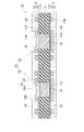
以下、本発明の第1実施形態を図1〜図8に基づいて説明する。図1に示すように、本実施形態の配線板10では、絶縁性部材からなると共に可撓性を有する絶縁基板11(本発明の「基板」に相当する)の表裏の両面上に、導体層12,12が形成されている。導体層12,12のうち、絶縁基板11の表側の面であるF面11F側の導体層12が本発明の第2導体層12Aに相当し、絶縁基板11の裏側の面であるB面11B側の導体層12が本発明の第1導体層12Bに相当する。
[First Embodiment]
Hereinafter, a first embodiment of the present invention will be described with reference to FIGS. As shown in FIG. 1, in the
導体層12は、絶縁基板11上に設けられている銅箔層18(本発明の「金属箔層」に相当する)と、銅箔層18上の銅メッキ層19(本発明の「金属メッキ層」に相当する)とを有している。表裏の導体層12,12上には、カバーレイ25,25がそれぞれ積層されている。また、絶縁基板11のF面11F側のカバーレイ25には、複数のパッド用孔25Hが形成され、導体層12のうちパッド用孔25Hから露出した部分がパッド26(本発明の「電子部品接続部」に相当する)になっている。なお、絶縁基板11と導体層12とは接着シート11Dによって接着されている。以降、単に「絶縁基板11」というときは、これら接着シート11Dを含めたものを指す。
The
ここで、本実施形態の配線板10では、絶縁基板11に複数の絶縁貫通孔11H(本発明の「貫通孔」に相当する)が設けられている。そして、これら絶縁貫通孔11Hには、例えば銅製のメッキポスト14が隙間なく嵌合されている。メッキポスト14は、第1導体層12Bの銅箔層18から突出していて、その先端面は、絶縁貫通孔11H内に位置している。また、メッキポスト14同士の高さには僅かにばらつきがあり、図1における右側のメッキポスト14は左側のメッキポスト14よりも僅かに高くなっている。
Here, in the
第2導体層12Aには、絶縁基板11の絶縁貫通孔11Hと重なる第2導体貫通孔12K(本発明の「貫通孔」に相当する)が設けられている。そして、絶縁貫通孔11H内におけるメッキポスト14より上方部分及び第2導体貫通孔12K内には銅メッキが施されていて、メッキポスト14に接続するメッキ接続部20が形成されている。メッキ接続部20は、第2導体層12Aにおける銅メッキ層19と一体に形成されている。このメッキ接続部20によって、メッキポスト14と第2導体層12Aとの間が接続されると共に、メッキ接続部20とメッキポスト14とによって、表裏の導体層12,12同士の間が接続されている。なお、上述したパッド26は、第2導体貫通孔12Kの上方領域に配され、導体層12,12のうちパッド用孔25Hから露出した部分とメッキ接続部20のうちパッド用孔25Hから露出した部分とから構成されている。メッキ接続部20のうちパッド用孔25Hから露出した部分の上面は導体層12のうちパッド用孔25Hから露出した部分の上面よりも低くなっていて、これにより、パッド26に凹部26Aが形成されている。
The
本実施形態の配線板10は、以下のようにして製造される。
(1)図2(A)に示すように、支持基板50の表側の面であるF面50Fに、キャリア付き銅箔33が重ねられる。キャリア付き銅箔33は、キャリア34と、第1導体層12Bの銅箔層18となる銅箔35と、を重ね、キャリア34と銅箔35との外周部同士を接着してなる。キャリア付き銅箔33は、キャリア34をF面30F側に向けて配置される。
The
(1) As shown in FIG. 2A, a
(2)図2(B)に示すように、銅箔35上にメッキレジスト37が形成される。
(2) A
(3)電解メッキ処理が行われ、図3(A)に示すように、銅箔35のうちメッキレジスト37から露出している部分に銅メッキが充填される。
(3) An electrolytic plating process is performed, and as shown in FIG. 3 (A), the copper plating is filled in the portion of the
(4)メッキレジスト37が剥離されて、図3(B)に示すように、銅箔35上にメッキポスト14が形成される。なお、各メッキポスト14の高さにはばらつきが生じる。
(4) The
(5)ポリイミド樹脂からなる可撓性の絶縁基板11と、2枚の接着シート11D,11Dと、第2導体層12Aの銅箔層18となる銅箔35とが用意される。絶縁基板11には、絶縁貫通孔11Hが設けられ、接着シート11D,11Dと、銅箔35とにも、絶縁貫通孔11Hと重なる貫通孔が設けられる。そして、図4に示すように、キャリア付き銅箔33に対して、キャリア付き銅箔33側から、接着シート11D、絶縁基板11、接着シート11D、銅箔35の順に重ねられる。
(5) A
(6)加熱プレス処理が行われ、図5(A)に示すように、支持基板50、キャリア付き銅箔33、絶縁基板11及び銅箔35が一体化する。これにより、絶縁基板11の表裏に銅箔35が貼り合わされると共に、メッキポスト14が絶縁基板11の絶縁貫通孔11Hに圧入されて隙間なく嵌合する。
(6) A heat press process is performed, and as shown to FIG. 5 (A), the
(7)図5(B)に示すように、支持基板50とキャリア34とが剥離される。
(7) As shown in FIG. 5B, the
(8)無電解メッキ処理が行われ、F面11F側及びB面11B側の銅箔35,35上と、メッキポスト14の上面、F面11F側の銅箔35の貫通孔(第2導体貫通孔12K)内に図示しない無電解メッキ膜が形成される。
(8) Electroless plating treatment is performed, and through holes (second conductors) on the
(9)電解メッキ処理が行われ、図6(A)に示すように、無電解メッキ膜(図示せず)上に銅メッキ膜38(本発明の「金属メッキ膜」に相当する)が形成される。これにより、銅箔35,35上に銅メッキが施されると共に、第2導体貫通孔12K内に銅メッキが充填される。
(9) Electrolytic plating is performed, and a copper plating film 38 (corresponding to the “metal plating film” of the present invention) is formed on an electroless plating film (not shown) as shown in FIG. Is done. Thereby, copper plating is performed on the
(10)図6(B)に示すように、銅メッキ膜38上にエッチングレジスト39が形成される。
(10) As shown in FIG. 6B, an
(11)エッチングが行われ、図7(A)に示すように、銅メッキ膜38、無電解メッキ膜及び銅箔35のうちエッチングレジスト39から露出している部分が除去される。
(11) Etching is performed, and as shown in FIG. 7A, portions of the
(12)エッチングレジスト39が剥離され、図7(B)に示すように、残された銅箔35、無電解メッキ膜及び銅メッキ膜38から、銅箔層18と銅メッキ層19とを有する導体層12が形成されると共に、第2導体貫通孔12K内に充填されている銅メッキにより、F面11F側の第2導体層12Aとメッキポスト14とを接続するメッキ接続部20が形成される。
(12) The
(13)絶縁基板11の表裏の導体層12,12上にカバーレイ25,25が積層される。なお、F面11F側のカバーレイ25には、予めパッド用孔25Hが形成されていて、第2導体層12A及びメッキ接続部20のうちパッド用孔25Hから露出している部分がパッド26となる。以上で図1に示される配線板10が完成する。
(13) Coverlays 25 and 25 are laminated on the conductor layers 12 and 12 on the front and back sides of the insulating
本実施形態の配線板10の構造及び製造方法に関する説明は以上である。次に配線板10の使用例と作用効果とを説明する。本実施形態の配線板10は、例えば、図8に示すように、パッド26上に半田バンプ28が形成されて、その上にLED80等が搭載されて半田付けされることで使用される。なお、LED80と接続されている2つのパッド26,26から本発明の電子部品実装部29が構成されている。
This completes the description of the structure and manufacturing method of the
本実施形態の配線板10では、絶縁基板11にメッキポスト14が嵌合され、このメッキポスト14がメッキ接続部20を介してLED80に接続されているので、LED80からの放熱が効率よく行われ、LED80における不具合の発生が防がれる。また、1つのLED80に対して2つのメッキポスト14,14が接続される(即ち、1つの電子部品実装部29に対して2つのメッキポスト14,14が接続されている)ので、LED80からの放熱がより効率よく行われれる。
In the
ところで、従来の配線板では、放熱用の金属部材の嵌合が金型を用いて行われていたが、従来の配線板では、例えば、金属部材の大きさが異なるものを数種類試作する際に、その都度金型を作成する必要があり、コストがかかるという問題が考えられる。 By the way, in the conventional wiring board, the metal member for heat dissipation was fitted using a metal mold. However, in the conventional wiring board, for example, when several types of metal members having different sizes are manufactured as prototypes. It is necessary to create a mold each time, and there is a problem that it is expensive.
これに対して、本実施形態の配線板10では、メッキポスト14が、銅箔35上に銅メッキが施されることにより形成され、かつ、その銅箔35が絶縁基板11に積層されることで、絶縁基板11の絶縁貫通孔11Hに嵌合されるので、所望する金属部材に合わせて金型を作成する必要がなく、コストを削減することができる。また、メッキポスト14が銅箔35上に形成されるので、複数のメッキポスト14を一度に形成することができ、それらの絶縁基板11への嵌合も一度に行うことができる。また、それらメッキポスト14は、形成されると同時に第1導体層12Bの銅箔層18となる銅箔35に位置決めされるため、絶縁貫通孔11Hへの圧入がスムーズとなる。
On the other hand, in the
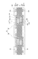
[第2実施形態]
図9に示される第2実施形態の配線板10Vは、メッキポスト14が、第1導体層12Bと第2導体層12Aとの両方に設けられている点が上記第1実施形態と異なる。以降、第1導体層12Bに設けられているメッキポスト14を、適宜、第1メッキポスト14Bといい、第2導体層12Aに設けられているメッキポスト14を、適宜、第2メッキポスト14Aという。
[Second Embodiment]
The
第1メッキポスト14Bと第2メッキポスト14Aとは、絶縁貫通孔11H内で互いに突き合わされている。なお、ここでいう「突き合わされる」とは、第1メッキポスト14Bと第2メッキポスト14Aとの先端同士が当接している場合だけではなく、先端同士の間に僅かに隙間がある場合も含む。また、配線板10Vには、第1導体層12Bの銅箔層18、第1メッキポスト14B、第2メッキポスト14A及び第2導体層12Aの銅箔層18を合わせて貫通する連続ポスト貫通孔15が形成されると共に、この連続ポスト貫通孔15にメッキが充填されてなる連続メッキ接続ライン21(本発明の「メッキ接続部」に相当する)が設けられている。なお、連続ポスト貫通孔15のうち第1メッキポスト14Bを貫通している部分が本発明の「第1孔」に相当する第1ポスト貫通孔15Bに相当し、第2メッキポスト14Aを貫通している部分が本発明の「第2孔」に相当する第2ポスト貫通孔15Aに相当する。また、連続メッキ接続ライン21のうち、第1ポスト貫通孔15Bに設けられている部分を、適宜、第1メッキ接続ライン21Bといい、第2ポスト貫通孔15Aに設けられている部分を、適宜、第2メッキ接続ライン21Aという。この連続メッキ接続ライン21によって、第1メッキポスト14Bと第2導体層12Aとが接続されると共に、第2メッキポスト14Aと第1導体層12Bとが接続される。
The
本実施形態の配線板10Vは、以下のようにして製造される。
(1)支持基板50の表側の面であるF面50Fに、キャリア付き銅箔33が重ねられたものと、支持基板50の裏側の面であるB面50Bに、キャリア付き銅箔33が重ねられたものと、が用意される。これらキャリア付き銅箔33,33の銅箔35,35には、それぞれ、メッキポスト14,14が形成される。
The
(1) The copper foil with
(2)絶縁貫通孔11Hが形成されている絶縁基板11と、絶縁貫通孔11Hに重なる貫通孔が形成されている2枚の接着シート11D,11Dと、が用意される。そして、接着シート11D、絶縁基板11、接着シート11D、銅箔35の順に重ねられ、2つのキャリア付き銅箔33,33の間に配される。
(2) The insulating
(3)加熱プレス処理が行われ、図10(A)に示すように、支持基板50,50、キャリア付き銅箔33,33及び絶縁基板11が一体化する。これにより、絶縁基板11の表裏に銅箔35,35が貼り合わされると共に、メッキポスト14,14が絶縁基板11の絶縁貫通孔11Hに圧入されて隙間なく嵌合する。このとき、表裏のメッキポスト14,14同士が突き合わされる。
(3) A heat press process is performed, and as shown to FIG. 10 (A), the
(4)図10(B)に示すように、支持基板50とキャリア34とが剥離される。
(4) As shown in FIG. 10B, the
(5)図11(A)に示すように、ドリル等の工具により、表裏の銅箔35,35とメッキポスト14,14とを貫通する連続ポスト貫通孔15が形成される。
(5) As shown in FIG. 11 (A), a continuous post through
(6)無電解メッキ処理が行われ、F面11F側及びB面11B側の銅箔35,35上と、連続ポスト貫通孔15内とに図示しない無電解メッキ膜が形成される。
(6) An electroless plating process is performed, and an electroless plating film (not shown) is formed on the copper foils 35 and 35 on the
(7)電解メッキ処理が行われ、図11(B)に示すように、無電解メッキ膜(図示せず)上に銅メッキ膜38(本発明の「金属メッキ膜」に相当する)が形成される。これにより、銅箔35,35上に銅メッキが施されると共に、連続ポスト貫通孔15内に銅メッキが充填される。
(7) An electrolytic plating process is performed to form a copper plating film 38 (corresponding to the “metal plating film” of the present invention) on an electroless plating film (not shown) as shown in FIG. Is done. As a result, copper plating is performed on the copper foils 35 and 35 and the continuous post through
(8)上記第1実施形態における(10)〜(13)と同様の処理が行われ、図9に示される配線板10Vが完成する。
(8) The same processing as (10) to (13) in the first embodiment is performed, and the
本実施形態の配線板10Vの構造及び製造方法に関する説明は以上である。本実施形態の配線板10Vによれば、絶縁貫通孔11Hの延長線上の導体層12,12が共に、銅箔層18と銅メッキ層19との2層構造となっているため、表裏の導体層12,12の平坦性を向上することができる。
This completes the description of the structure and manufacturing method of the
また、例えば、支持基板50の表裏にキャリア付き銅箔33を張り合わせたものを複数用意して、複数の絶縁基板11と交互に並べて加熱プレス処理することで、銅箔35が貼り合わされた絶縁基板11を一度に複数得ることができる。
In addition, for example, a plurality of substrates with the carrier-attached
[他の実施形態]
本発明は、前記実施形態に限定されるものではなく、例えば、以下に説明するような実施形態も本発明の技術的範囲に含まれ、さらに、下記以外にも要旨を逸脱しない範囲内で種々変更して実施することができる。
[Other Embodiments]
The present invention is not limited to the above-described embodiment. For example, the embodiments described below are also included in the technical scope of the present invention, and various other than the following can be made without departing from the scope of the invention. It can be changed and implemented.
(1)上記実施形態では、導体層12が、絶縁基板11の表裏に1層ずつ形成されていたが、絶縁樹脂層を挟んで複数層ずつ形成されていてもよい。
(1) In the above embodiment, the conductor layers 12 are formed one layer at a time on the front and back sides of the insulating
(2)上記実施形態では、パッド26上に実装される電子部品がLED80であったが、パワー半導体等であってもよい。
(2) In the above embodiment, the electronic component mounted on the
(3)上記第2実施形態では、第1メッキポスト14Bと第2メッキポスト14Aとを合わせて貫通する連続ポスト貫通孔15が形成されていたが、図12に示すように、第1メッキポスト14Bを貫通する第1ポスト貫通孔15Bと第2メッキポスト14Aを貫通する第2ポスト貫通孔15Aとをずらして形成する構成であってもよい。このとき、第1メッキ接続ライン21B及び第2メッキ接続ライン21Aが、本発明の「メッキ接続部」にそれぞれ相当する。
(3) In the second embodiment, the continuous post through
(4)上記実施形態では、配線板10の裏側にパッド26が形成されていなかったが、図13に示すように、裏側にもパッド26を形成し、例えば、金属板90と接続する構成であってもよい。この場合、メッキポスト14の熱が金属板90に排熱されるため、LED80の放熱がより効果的に行われる。
(4) In the above embodiment, the
(5)配線板10のパッド26とLED80とをワイヤボンディングにより接続してもよい。
(5) The
(6)上記実施形態では、メッキポスト14が銅製であったが、これに限られるものではなく、例えば、銀製であってもよいし、銅にモリブデンやタングステンを混ぜたものや、アルミニウム等であってもよい。
(6) In the above embodiment, the plating
(7)上記実施形態では、メッキポスト14の先端面が、絶縁貫通孔11H内に位置していたが、絶縁基板11の上面と面一であってもよい。
(7) In the above embodiment, the tip surface of the
10,10V 配線板
11 絶縁基板(基板)
11H 絶縁貫通孔(貫通孔)
12 導体層
12A 第2導体層
12B 第1導体層
12K 第2導体貫通孔(貫通孔)
14 メッキポスト
14A 第2メッキポスト
14B 第1メッキポスト
15 連続ポスト貫通孔
15A 第2ポスト貫通孔(第2孔)
15B 第1ポスト貫通孔(第1孔)
18 銅箔層(金属箔層)
19 銅メッキ層(金属メッキ層)
20 メッキ接続部
21 連続メッキ接続ライン(メッキ接続部)
21A 第1メッキ接続ライン
21B 第1メッキ接続ライン
26 パッド(電子部品接続部)
35 銅箔(金属箔)
38 銅メッキ膜(金属メッキ膜)
10,
11H Insulated through hole (through hole)
12
14
15B First post through hole (first hole)
18 Copper foil layer (metal foil layer)
19 Copper plating layer (metal plating layer)
20
21A First plating
35 Copper foil (metal foil)
38 Copper plating film (metal plating film)
Claims (17)
前記基板の表裏の一方に積層されている第1導体層と、
前記基板の表裏の他方に積層されている第2導体層と、
前記基板に形成されている貫通孔と、
前記第1導体層から突出し、前記貫通孔に嵌合されている第1メッキポストと、
前記第2導体層と前記第1メッキポストとを接続するメッキ接続部と、
電子部品が実装されるための電子部品実装部と、を有し、
1つの前記電子部品が実装されるための1つの前記電子部品実装部は、前記第1導体層又は前記第2導体層における複数の前記貫通孔の上にそれぞれ位置して前記電子部品と接続される電子部品接続部を複数有し、複数の前記第1メッキポスト及び複数の前記メッキ接続部と接続されている配線板。 An insulating substrate;
A first conductor layer laminated on one of the front and back sides of the substrate;
A second conductor layer laminated on the other of the front and back of the substrate;
A through hole formed in the substrate;
A first plating post protruding from the first conductor layer and fitted into the through hole;
A plating connection portion connecting the second conductor layer and the first plating post;
An electronic component mounting part for mounting the electronic component,
One electronic component mounting portion for mounting one electronic component is located on each of the plurality of through holes in the first conductor layer or the second conductor layer and connected to the electronic component. A wiring board having a plurality of electronic component connection portions connected to the plurality of first plating posts and the plurality of plating connection portions.
前記メッキ接続部は、前記第2導体層と前記第1メッキポストの先端とを接続する。 The wiring board according to claim 1,
The plating connection portion connects the second conductor layer and the tip of the first plating post.
前記第2導体層は、金属箔層と、前記金属箔層上に設けられている金属メッキ層と、を有し、
前記金属メッキ層と前記メッキ接続部とは一体に形成されている。 The wiring board according to claim 2,
The second conductor layer has a metal foil layer, and a metal plating layer provided on the metal foil layer,
The metal plating layer and the plating connection portion are integrally formed.
前記第1メッキポストの先端面は、前記貫通孔内に位置している。 The wiring board according to any one of claims 1 to 3,
The front end surface of the first plating post is located in the through hole.
さらに、前記第2導体層から突出して、前記貫通孔に嵌合され、前記第1メッキポストに突き合わされる第2メッキポストを備える。 The wiring board according to claim 1,
Furthermore, a second plating post that protrudes from the second conductor layer, is fitted into the through hole, and is abutted against the first plating post is provided.
前記第2メッキポストには、前記基板の板厚方向で前記第2メッキポストを貫通する第2孔が形成され、
前記メッキ接続部は、前記第2孔内に形成されている。 The wiring board according to claim 5,
A second hole penetrating the second plating post in the thickness direction of the substrate is formed in the second plating post.
The plated connection portion is formed in the second hole.
前記第1メッキポストには、前記第2孔の延長線上で前記第1メッキポストを貫通する第1孔が形成され、
前記メッキ接続部は、前記第1孔内及び前記第2孔内に形成されている。 The wiring board according to claim 6,
The first plating post is formed with a first hole penetrating the first plating post on an extension line of the second hole,
The plated connection portion is formed in the first hole and the second hole.
前記基板は、可撓性を有している。 The wiring board according to any one of claims 1 to 7,
The substrate has flexibility.
前記貫通孔を有する前記基板と、前記第1メッキポストが突出している金属箔を用意することと、
前記金属箔を、前記基板の表裏の一方に積層して、前記第1メッキポストを前記貫通孔に嵌合して収容することと、
前記金属箔を使用して前記第1導体層を形成することと、を含む。 An insulating substrate, a first conductor layer laminated on one of the front and back sides of the substrate, a second conductor layer laminated on the other side of the substrate, and a through hole formed in the substrate A method of manufacturing a wiring board comprising: a first plating post that is accommodated and connected to the first conductor layer; and a plating connection portion that connects the second conductor layer and the first plating post.
Preparing the substrate having the through hole and a metal foil from which the first plating post protrudes;
Laminating the metal foil on one of the front and back sides of the substrate, and fitting the first plating post into the through-hole to accommodate it;
Forming the first conductor layer using the metal foil.
前記基板の表裏の他方に金属箔を積層して、その金属箔を使用して前記第2導体層を形成することと、
前記第2導体層用の前記金属箔に、前記基板の前記貫通孔に重なる貫通孔を形成することと、
前記基板の前記貫通孔内及び前記第2導体層用の前記金属箔の前記貫通孔内にメッキを行うことで前記メッキ接続部を形成することと、
前記メッキ接続部により、前記第2導体層と前記第1メッキポストの先端とを接続することと、を行う。 It is a manufacturing method of the wiring board according to claim 9,
Laminating a metal foil on the other side of the front and back of the substrate, and using the metal foil to form the second conductor layer;
Forming a through hole overlapping the through hole of the substrate in the metal foil for the second conductor layer;
Forming the plated connection portion by plating in the through hole of the substrate and in the through hole of the metal foil for the second conductor layer;
The second conductor layer and the tip of the first plating post are connected by the plating connecting portion.
前記メッキ接続部の形成と共に、前記第2導体層用の前記金属箔に金属メッキ膜を積層することと、
記第2導体層用の前記金属箔と前記金属メッキ膜とをエッチングすることにより前記第2導体層を形成することと、を行う。 It is a manufacturing method of the wiring board according to claim 10,
Along with the formation of the plating connection portion, laminating a metal plating film on the metal foil for the second conductor layer;
The second conductor layer is formed by etching the metal foil for the second conductor layer and the metal plating film.
前記第1メッキポストの先端面を、前記貫通孔内に位置させる。 A method for manufacturing a wiring board according to any one of claims 9 to 11,
The front end surface of the first plating post is positioned in the through hole.
さらに、第2メッキポストが突出している金属箔を用意することと、
その金属箔を、前記基板の表裏の他方に積層して、前記第2メッキポストを前記貫通孔に嵌合させ、かつ、前記第1メッキポストに突き合わせることと、
その金属箔を使用して前記第2導体層を形成することと、を含む。 It is a manufacturing method of the wiring board according to claim 9,
Furthermore, preparing a metal foil from which the second plating post protrudes;
Laminating the metal foil on the other side of the front and back of the substrate, fitting the second plating post into the through-hole, and abutting the first plating post;
Forming the second conductor layer using the metal foil.
前記基板の板厚方向で前記第2メッキポストを貫通する第2孔を形成することと、
前記第2孔内にメッキを充填することで前記メッキ接続部を形成することと、を行う。 It is a manufacturing method of the wiring board according to claim 13,
Forming a second hole penetrating the second plating post in the thickness direction of the substrate;
The plating connection portion is formed by filling the second hole with plating.
前記第2孔の延長線上で前記第1メッキポストを貫通する第1孔を形成することと、
前記第1孔内及び前記第2孔内にメッキを充填することで前記メッキ接続部を形成することと、を行う。 It is a manufacturing method of the wiring board according to claim 14,
Forming a first hole penetrating the first plating post on an extension line of the second hole;
The plating connection portion is formed by filling the first hole and the second hole with plating.
前記基板を、可撓性部材により構成する。 A method for manufacturing a wiring board according to any one of claims 9 to 15,
The substrate is made of a flexible member.
前記第1導体層又は前記第2導体層における複数の前記貫通孔の上に、電子部品と接続するための電子部品接続部をそれぞれ形成し、
複数の前記電子部品接続部から1つの電子部品が実装される1つの電子部品実装部を構成し、1つの前記電子部品実装部を複数の前記第1メッキポスト及び複数の前記メッキ接続部と接続する。 A method for manufacturing a wiring board according to any one of claims 9 to 16,
On each of the plurality of through holes in the first conductor layer or the second conductor layer, an electronic component connection portion for connecting to an electronic component is formed, respectively.
One electronic component mounting portion on which one electronic component is mounted is formed from the plurality of electronic component connecting portions, and one electronic component mounting portion is connected to the plurality of first plating posts and the plurality of plating connecting portions. To do.
Priority Applications (2)
| Application Number | Priority Date | Filing Date | Title |
|---|---|---|---|
| JP2015241764A JP2017108034A (en) | 2015-12-11 | 2015-12-11 | Wiring board and method of manufacturing the same |
| US15/375,297 US9750136B2 (en) | 2015-12-11 | 2016-12-12 | Wiring board and method for manufacturing the same |
Applications Claiming Priority (1)
| Application Number | Priority Date | Filing Date | Title |
|---|---|---|---|
| JP2015241764A JP2017108034A (en) | 2015-12-11 | 2015-12-11 | Wiring board and method of manufacturing the same |
Publications (1)
| Publication Number | Publication Date |
|---|---|
| JP2017108034A true JP2017108034A (en) | 2017-06-15 |
Family
ID=59018571
Family Applications (1)
| Application Number | Title | Priority Date | Filing Date |
|---|---|---|---|
| JP2015241764A Pending JP2017108034A (en) | 2015-12-11 | 2015-12-11 | Wiring board and method of manufacturing the same |
Country Status (2)
| Country | Link |
|---|---|
| US (1) | US9750136B2 (en) |
| JP (1) | JP2017108034A (en) |
Cited By (1)
| Publication number | Priority date | Publication date | Assignee | Title |
|---|---|---|---|---|
| US11699688B2 (en) | 2019-12-03 | 2023-07-11 | Nichia Corporation | Surface-emitting light source and method of manufacturing the same |
Family Cites Families (7)
| Publication number | Priority date | Publication date | Assignee | Title |
|---|---|---|---|---|
| JP2005209861A (en) * | 2004-01-22 | 2005-08-04 | Nippon Steel Corp | Wafer-level package and method for manufacturing the same |
| TWI335785B (en) * | 2006-10-19 | 2011-01-01 | Unimicron Technology Corp | Circuit board structure and fabrication method thereof |
| JP2011187477A (en) | 2010-03-04 | 2011-09-22 | Nhk Spring Co Ltd | Manufacturing method for metal base circuit board, and metal base circuit board |
| KR101255954B1 (en) * | 2011-12-22 | 2013-04-23 | 삼성전기주식회사 | Printed circuit board and manufacturing method thereof |
| KR20150064976A (en) * | 2013-12-04 | 2015-06-12 | 삼성전기주식회사 | Printed circuit board and manufacturing method thereof |
| US10420204B2 (en) * | 2014-03-07 | 2019-09-17 | Bridge Semiconductor Corporation | Wiring board having electrical isolator and moisture inhibiting cap incorporated therein and method of making the same |
| JP2017050315A (en) * | 2015-08-31 | 2017-03-09 | イビデン株式会社 | Printed wiring board and method of manufacturing the same |
-
2015
- 2015-12-11 JP JP2015241764A patent/JP2017108034A/en active Pending
-
2016
- 2016-12-12 US US15/375,297 patent/US9750136B2/en not_active Expired - Fee Related
Cited By (1)
| Publication number | Priority date | Publication date | Assignee | Title |
|---|---|---|---|---|
| US11699688B2 (en) | 2019-12-03 | 2023-07-11 | Nichia Corporation | Surface-emitting light source and method of manufacturing the same |
Also Published As
| Publication number | Publication date |
|---|---|
| US9750136B2 (en) | 2017-08-29 |
| US20170171974A1 (en) | 2017-06-15 |
Similar Documents
| Publication | Publication Date | Title |
|---|---|---|
| US9226382B2 (en) | Printed wiring board | |
| JP6226167B2 (en) | Multilayer wiring board | |
| TW201427510A (en) | Printed circuit board having buried component and method for manufacturing same | |
| JP2016219478A (en) | Wiring board and manufacturing method therefor | |
| JP2015012022A (en) | Printed wiring board | |
| JP2014107552A (en) | Multilayer printed circuit board and method of manufacturing the same | |
| JP2015035497A (en) | Electronic component built-in wiring board | |
| TW201427509A (en) | Printed circuit board having buried component and method for manufacturing same | |
| JP2018018936A (en) | Wiring board | |
| JP2013065810A (en) | Multilayer substrate | |
| JP2014216423A (en) | Wiring board, method of manufacturing wiring board | |
| JP2014090147A (en) | Wiring board and packaging structure employing the same | |
| JP2017108034A (en) | Wiring board and method of manufacturing the same | |
| KR100674305B1 (en) | Printed circuit board and manufacturing method thereof | |
| JP2013145847A (en) | Printed wiring board and manufacturing method of the same | |
| US10051736B2 (en) | Printed wiring board and method for manufacturing printed wiring board | |
| JPWO2015118951A1 (en) | Resin multilayer board and component module | |
| JP2019091897A (en) | Component mounting resin substrate | |
| JP2017108033A (en) | Wiring board and method of manufacturing the same | |
| US9443830B1 (en) | Printed circuits with embedded semiconductor dies | |
| TW201427505A (en) | Printed circuit board having buried component and method for manufacturing same | |
| JP5800076B2 (en) | Electronic device and electronic device mounting structure | |
| JP2018137343A (en) | Printed circuit board and inverter | |
| JP2017228644A (en) | Wiring board, composite wiring board including the wiring board, and method for their manufacturing | |
| JP2011243796A (en) | Electronic equipment and attachment structure of electronic equipment |