JP2017103303A - Adhesive for semiconductor, semiconductor device, and method for manufacturing the same - Google Patents
Adhesive for semiconductor, semiconductor device, and method for manufacturing the same Download PDFInfo
- Publication number
- JP2017103303A JP2017103303A JP2015233900A JP2015233900A JP2017103303A JP 2017103303 A JP2017103303 A JP 2017103303A JP 2015233900 A JP2015233900 A JP 2015233900A JP 2015233900 A JP2015233900 A JP 2015233900A JP 2017103303 A JP2017103303 A JP 2017103303A
- Authority
- JP
- Japan
- Prior art keywords
- adhesive
- semiconductors
- semiconductor
- semiconductor device
- component
- Prior art date
- Legal status (The legal status is an assumption and is not a legal conclusion. Google has not performed a legal analysis and makes no representation as to the accuracy of the status listed.)
- Pending
Links
Images


Classifications
-
- H—ELECTRICITY
- H01—ELECTRIC ELEMENTS
- H01L—SEMICONDUCTOR DEVICES NOT COVERED BY CLASS H10
- H01L2224/00—Indexing scheme for arrangements for connecting or disconnecting semiconductor or solid-state bodies and methods related thereto as covered by H01L24/00
- H01L2224/01—Means for bonding being attached to, or being formed on, the surface to be connected, e.g. chip-to-package, die-attach, "first-level" interconnects; Manufacturing methods related thereto
- H01L2224/10—Bump connectors; Manufacturing methods related thereto
- H01L2224/15—Structure, shape, material or disposition of the bump connectors after the connecting process
- H01L2224/16—Structure, shape, material or disposition of the bump connectors after the connecting process of an individual bump connector
- H01L2224/161—Disposition
- H01L2224/16135—Disposition the bump connector connecting between different semiconductor or solid-state bodies, i.e. chip-to-chip
- H01L2224/16145—Disposition the bump connector connecting between different semiconductor or solid-state bodies, i.e. chip-to-chip the bodies being stacked
-
- H—ELECTRICITY
- H01—ELECTRIC ELEMENTS
- H01L—SEMICONDUCTOR DEVICES NOT COVERED BY CLASS H10
- H01L2224/00—Indexing scheme for arrangements for connecting or disconnecting semiconductor or solid-state bodies and methods related thereto as covered by H01L24/00
- H01L2224/73—Means for bonding being of different types provided for in two or more of groups H01L2224/10, H01L2224/18, H01L2224/26, H01L2224/34, H01L2224/42, H01L2224/50, H01L2224/63, H01L2224/71
- H01L2224/732—Location after the connecting process
- H01L2224/73201—Location after the connecting process on the same surface
- H01L2224/73203—Bump and layer connectors
- H01L2224/73204—Bump and layer connectors the bump connector being embedded into the layer connector
Abstract
Description
本発明は、半導体用接着剤、半導体装置、及び半導体装置の製造方法に関する。 The present invention relates to a semiconductor adhesive, a semiconductor device, and a method for manufacturing a semiconductor device.
従来、半導体チップと基板を接続するには金ワイヤ等の金属細線を用いるワイヤーボンディング方式が広く適用されてきたが、半導体装置に対する高機能・高集積・高速化等の要求に対応するため、半導体チップ又は基板にバンプと呼ばれる導電性突起を形成して、半導体チップと基板間で直接接続するフリップチップ接続方式(FC接続方式)が広まりつつある。 Conventionally, a wire bonding method using a fine metal wire such as a gold wire has been widely applied to connect a semiconductor chip and a substrate. However, in order to meet demands for high functionality, high integration, high speed, etc., for semiconductor devices, A flip chip connection method (FC connection method) in which conductive protrusions called bumps are formed on a chip or a substrate to directly connect the semiconductor chip and the substrate is becoming widespread.
フリップチップ接続方式としては、はんだ、スズ、金、銀、銅等を用いて金属接合させる方法、超音波振動を印加して金属接合させる方法、樹脂の収縮力によって機械的接触を保持する方法などが知られているが、接続部の信頼性の観点から、はんだ、スズ、金、銀、銅等を用いて金属接合させる方法が一般的である。 Flip chip connection methods include metal bonding using solder, tin, gold, silver, copper, etc., metal bonding by applying ultrasonic vibration, method of maintaining mechanical contact by the shrinkage force of the resin, etc. However, from the viewpoint of the reliability of the connection portion, a method of metal bonding using solder, tin, gold, silver, copper, or the like is common.
例えば、半導体チップと基板間の接続においては、BGA(Ball Grid Array)、CSP(Chip Size Package)等に盛んに用いられているCOB(Chip On Board)型の接続方式もフリップチップ接続方式である。また、フリップチップ接続方式は、半導体チップ上にバンプ又は配線を形成して、半導体チップ間で接続するCOC(Chip On Chip)型の接続方式にも広く用いられている(例えば、下記特許文献1参照)。 For example, in connection between a semiconductor chip and a substrate, a COB (Chip On Board) type connection method that is actively used in BGA (Ball Grid Array), CSP (Chip Size Package), etc. is also a flip chip connection method. . The flip chip connection method is also widely used in a COC (Chip On Chip) type connection method in which bumps or wirings are formed on semiconductor chips to connect the semiconductor chips (for example, Patent Document 1 below). reference).
更なる小型化、薄型化、高機能化が強く要求されたパッケージでは、上述した接続方式を積層・多段化したチップスタック型パッケージ、POP(Package On Package)、TSV(Through−Silicon Via)等も広く普及し始めている。平面状でなく立体状に配置することでパッケージを小さくできることから、これらの技術は多用され、半導体の性能向上及びノイズ低減、実装面積の削減、省電力化にも有効であり、次世代の半導体配線技術として注目されている。 For packages that are strongly required to be further reduced in size, thickness, and functionality, there are chip stack type packages, POP (Package On Package), TSV (Through-Silicon Via), etc., in which the above connection methods are stacked and multi-staged. It has begun to spread widely. Since the package can be made smaller by arranging it in a three-dimensional shape instead of a flat shape, these technologies are frequently used, and it is also effective for improving semiconductor performance, reducing noise, reducing mounting area, and reducing power consumption. It is attracting attention as a wiring technology.
また、生産性向上の観点から、ウエハ上に半導体チップを圧着(接続)した後に個片化して半導体パッケージを作製するCOW(Chip On Wafer)、ウエハ同士を圧着(接続)した後に個片化して半導体パッケージを作製するWOW(Wafer On Wafer)も注目されている。さらに、ウエハ上又はマップ基板上に複数のチップの位置合わせをして仮圧着した後、複数のチップを一括で圧着して接続を確保するギャングボンディング方式も、生産性向上の観点から注目されている。 Also, from the viewpoint of improving productivity, COW (Chip On Wafer) for manufacturing a semiconductor package by bonding a semiconductor chip onto a wafer after being crimped (connected), and individualizing after bonding (connecting) the wafers together A WOW (Wafer On Wafer) for manufacturing a semiconductor package has also attracted attention. Furthermore, a gang bonding method in which a plurality of chips are aligned on a wafer or a map substrate and temporarily crimped and then a plurality of chips are crimped together to ensure connection is also attracting attention from the viewpoint of improving productivity. Yes.
上述した様々な接続方法で用いられる半導体用接着剤には、吸湿後に260℃前後のリフロ炉に通しても、接続不良、剥離及びボイド発生を抑制可能な耐リフロ性、更には接着力の向上が強く求められている。しかし、従来の半導体用接着剤では、耐熱性及び吸湿後の接着力、更には耐リフロ性が低く、接続不良、剥離等の問題が生じる場合がある。特に、アクリル硬化系接着剤のような短時間でボイドなく半導体装置を製造できる半導体接着剤では、接着力の向上が困難である。 The adhesive for semiconductors used in the various connection methods described above has improved reflow resistance and improved adhesion that can suppress poor connection, peeling and void generation even after passing through a reflow oven at around 260 ° C after moisture absorption. Is strongly demanded. However, conventional adhesives for semiconductors have low heat resistance, adhesive strength after moisture absorption, and reflow resistance, which may cause problems such as poor connection and peeling. In particular, it is difficult to improve the adhesive strength of a semiconductor adhesive that can manufacture a semiconductor device without voids in a short time, such as an acrylic curable adhesive.
本発明は、上述した課題を解決するためになされたものであり、アクリル硬化系接着剤であっても、耐リフロ性及び接着力に優れる半導体用接着剤、並びに該半導体用接着剤を用いた半導体装置及び半導体装置の製造方法を提供することを目的とする。 The present invention has been made in order to solve the above-described problems, and an adhesive for a semiconductor having excellent reflow resistance and adhesive force, and an adhesive for a semiconductor, are used even for an acrylic curable adhesive. It is an object to provide a semiconductor device and a method for manufacturing the semiconductor device.
本発明は、下記[1]〜[10]を提供する。
[1] (メタ)アクリル化合物と、硬化剤と、下記式(1)で表される化合物と、を含有する半導体用接着剤。

[式(1)中、R1は水素原子、メチル基又はエチル基を表し、R2、R3及びR4は、それぞれ独立に水素原子、−(CH2)m−CH3で表されるアルキル基、又はアルコキシ基を表し、かつR2、R3及びR4の少なくとも一つはメトキシ基を表し、mは0〜3の整数を表し、nは1〜6の整数を表す。]
[2] 重量平均分子量が10000以上の高分子化合物を更に含有する、[1]に記載の半導体用接着剤。
[3] 高分子化合物の重量平均分子量が30000以上であり、高分子化合物のガラス転移温度が100℃以下である、[2]に記載の半導体用接着剤。
[4] フィルム状である、[1]〜[3]のいずれかに記載の半導体用接着剤。
[5] (メタ)アクリル化合物が25℃で固形である、[1]〜[4]のいずれかに記載の半導体用接着剤。
[6] 硬化剤が熱ラジカル発生剤である、[1]〜[5]のいずれかに記載の半導体用接着剤。
[7] 硬化剤が過酸化物である、[1]〜[6]のいずれかに記載の半導体用接着剤。
[8] 半導体チップ及び配線回路基板のそれぞれの接続部が互いに電気的に接続された半導体装置、又は複数の半導体チップのそれぞれの接続部が互いに電気的に接続された半導体装置において接続部の封止に用いられる、[1]〜[7]のいずれかに記載の半導体用接着剤。
[9] [1]〜[8]のいずれかに記載の半導体用接着剤を用いる、半導体装置の製造方法。
[10] [1]〜[8]のいずれかに記載の半導体用接着剤又はその硬化物を備える半導体装置。
The present invention provides the following [1] to [10].
[1] A semiconductor adhesive containing a (meth) acrylic compound, a curing agent, and a compound represented by the following formula (1).
In Expression (1), R 1 represents a hydrogen atom, a methyl group or an ethyl group, R 2, R 3 and R 4 are each independently a hydrogen atom, - represented by (CH 2) m -CH 3 It represents an alkyl group or an alkoxy group, and at least one of R 2 , R 3 and R 4 represents a methoxy group, m represents an integer of 0 to 3, and n represents an integer of 1 to 6. ]
[2] The adhesive for semiconductors according to [1], further comprising a polymer compound having a weight average molecular weight of 10,000 or more.
[3] The semiconductor adhesive according to [2], wherein the polymer compound has a weight average molecular weight of 30000 or more and the polymer compound has a glass transition temperature of 100 ° C. or less.
[4] The semiconductor adhesive according to any one of [1] to [3], which is in the form of a film.
[5] The adhesive for semiconductors according to any one of [1] to [4], wherein the (meth) acrylic compound is solid at 25 ° C.
[6] The adhesive for semiconductors according to any one of [1] to [5], wherein the curing agent is a thermal radical generator.
[7] The adhesive for semiconductors according to any one of [1] to [6], wherein the curing agent is a peroxide.
[8] In a semiconductor device in which the connection portions of the semiconductor chip and the printed circuit board are electrically connected to each other, or in a semiconductor device in which the connection portions of the plurality of semiconductor chips are electrically connected to each other, sealing of the connection portions is performed. The adhesive for semiconductors in any one of [1]-[7] used for a stop.
[9] A method for manufacturing a semiconductor device, wherein the semiconductor adhesive according to any one of [1] to [8] is used.
[10] A semiconductor device comprising the semiconductor adhesive according to any one of [1] to [8] or a cured product thereof.
本発明によれば、アクリル硬化系接着剤であっても、耐リフロ性及び接着力に優れる半導体用接着剤、並びに該半導体用接着剤を用いた半導体装置及び半導体装置の製造方法を提供することができる。 ADVANTAGE OF THE INVENTION According to this invention, even if it is an acrylic hardening type adhesive agent, the adhesive agent for semiconductors which is excellent in reflow resistance and adhesive force, the semiconductor device using this adhesive agent for semiconductors, and the manufacturing method of a semiconductor device are provided. Can do.
以下、場合により図面を参照しつつ本発明の実施形態について詳細に説明する。なお、図面中、同一又は相当部分には同一符号を付し、重複する説明は省略する。また、上下左右等の位置関係は、特に断らない限り、図面に示す位置関係に基づくものとする。さらに、図面の寸法比率は図示の比率に限られるものではない。 Hereinafter, embodiments of the present invention will be described in detail with reference to the drawings as the case may be. In the drawings, the same or corresponding parts are denoted by the same reference numerals, and redundant description is omitted. Further, the positional relationship such as up, down, left and right is based on the positional relationship shown in the drawings unless otherwise specified. Further, the dimensional ratios in the drawings are not limited to the illustrated ratios.
本実施形態に係る接着剤は、半導体用接着剤として好適に用いられるものであり、(メタ)アクリル化合物(以下、場合により「(a)成分」という)と、硬化剤(以下、場合により「(b)成分」という)と、下記式(1)で表される化合物(以下、場合により「(c)成分」という)と、を含有する。
[式(1)中、R1は水素原子、メチル基又はエチル基を表し、R2、R3及びR4は、それぞれ独立に水素原子、−(CH2)m−CH3で表されるアルキル基、又はアルコキシ基を表し、かつR2、R3及びR4の少なくとも一つはメトキシ基を表し、mは0〜3の整数を表し、nは1〜6の整数を表す。]
The adhesive according to the present embodiment is suitably used as an adhesive for semiconductors, and includes a (meth) acrylic compound (hereinafter sometimes referred to as “component (a)”) and a curing agent (hereinafter sometimes referred to as “ (Referred to as “component (b)”) and a compound represented by the following formula (1) (hereinafter sometimes referred to as “component (c)”).
In Expression (1), R 1 represents a hydrogen atom, a methyl group or an ethyl group, R 2, R 3 and R 4 are each independently a hydrogen atom, - represented by (CH 2) m -CH 3 It represents an alkyl group or an alkoxy group, and at least one of R 2 , R 3 and R 4 represents a methoxy group, m represents an integer of 0 to 3, and n represents an integer of 1 to 6. ]
本実施形態に係る接着剤は、必要に応じて、重量平均分子量が10000以上の高分子化合物(以下、場合により「(d)成分」という)、フラックス剤、フィラー等を更に含有していてもよい。 The adhesive according to the present embodiment may further contain a polymer compound having a weight average molecular weight of 10,000 or more (hereinafter referred to as “component (d)” in some cases), a flux agent, a filler, and the like as necessary. Good.
((a)成分:(メタ)アクリル化合物)
(a)成分は、分子内に1個以上の(メタ)アクリロイル基を有する化合物であれば特に制限はない。ただし、(a)成分は、上記式(1)で表される化合物((c)成分)、及び後述する重量平均分子量が10000以上の高分子化合物((d)成分)を除く化合物である。例えば、ビスフェノールA型、ビスフェノールF型、ナフタレン型、フェノールノボラック型、クレゾールノボラック型、フェノールアラルキル型、ビフェニル型、トリフェニルメタン型、ジシクロペンタジエン型、フルオレン型、アダマンタン型、イソシアヌル酸型、各種多官能(メタ)アクリル化合物等を使用することができる。(a)成分は、耐熱性の観点から、ビスフェノールA、F型骨格、ナフタレン型骨格、フルオレン型骨格、アダマンタン型骨格、イソシアヌル酸型骨格含有アクリレートが好ましい。(a)成分は、1種単独で又は2種以上を併用して用いることができる。なお、「(メタ)アクリル化合物」は「アクリル化合物」及び「メタクリル化合物」、「(メタ)アクリロイル基」は「アクリロイル基」及び「メタクリロイル基」をそれぞれ意味する。
((A) component: (meth) acrylic compound)
The component (a) is not particularly limited as long as it is a compound having one or more (meth) acryloyl groups in the molecule. However, (a) component is a compound except the compound ((c) component) represented by the said Formula (1), and the high molecular compound ((d) component) whose weight average molecular weight mentioned later is 10,000 or more. For example, bisphenol A type, bisphenol F type, naphthalene type, phenol novolak type, cresol novolak type, phenol aralkyl type, biphenyl type, triphenylmethane type, dicyclopentadiene type, fluorene type, adamantane type, isocyanuric acid type, various types A functional (meth) acrylic compound or the like can be used. The component (a) is preferably bisphenol A, F-type skeleton, naphthalene-type skeleton, fluorene-type skeleton, adamantane-type skeleton, or isocyanuric acid-type skeleton-containing acrylate from the viewpoint of heat resistance. (A) A component can be used individually by 1 type or in combination of 2 or more types. “(Meth) acrylic compound” means “acrylic compound” and “methacrylic compound”, and “(meth) acryloyl group” means “acryloyl group” and “methacryloyl group”, respectively.
(a)成分の含有量は、接着剤の全量を基準として、10〜50質量%が好ましく、15〜40質量%がより好ましい。含有量が10質量%未満の場合、硬化成分が少ないため硬化後の樹脂の流動を充分に制御することが難しく、50質量%を超えると、硬化物が硬くなりすぎてパッケージの反りが大きくなる傾向がある。 The content of the component (a) is preferably 10 to 50% by mass and more preferably 15 to 40% by mass based on the total amount of the adhesive. When the content is less than 10% by mass, it is difficult to sufficiently control the flow of the resin after curing because there are few curing components. When the content exceeds 50% by mass, the cured product becomes too hard and the warpage of the package increases. Tend.
(a)成分は、室温(25℃)で固形であることが好ましい。液状に比べて固形のほうが、ボイドが発生しにくく、また、硬化前(Bステージ)の接着剤の粘性(タック)が小さく取り扱い性に優れる。室温(25℃)で固形である(a)成分としては、ビスフェノールA型骨格含有アクリレート、フルオレン型骨格含有アクリレート、アダマンタン型骨格含有アクリレート、イソシアヌル酸型骨格含有アクリレート等が挙げられる。 The component (a) is preferably solid at room temperature (25 ° C.). The solid is less likely to generate voids than the liquid, and the viscosity (tack) of the adhesive before curing (B stage) is small and excellent in handleability. Examples of the component (a) that is solid at room temperature (25 ° C.) include bisphenol A-type skeleton-containing acrylate, fluorene-type skeleton-containing acrylate, adamantane-type skeleton-containing acrylate, and isocyanuric acid-type skeleton-containing acrylate.
(a)成分における(メタ)アクリロイル基の官能基数は、3以下が好ましい。官能基数が4以上であると、官能基数が多いため短時間での硬化が充分に進行せず硬化反応率が低下する場合がある(硬化のネットワークが急速に進み、未反応基が残存する場合がある)。 The number of functional groups of the (meth) acryloyl group in the component (a) is preferably 3 or less. If the number of functional groups is 4 or more, curing in a short time may not proceed sufficiently because the number of functional groups is large, and the curing reaction rate may decrease (when the curing network proceeds rapidly and unreacted groups remain) There).
(a)成分の分子量は、10000未満であることが好ましく、5000以下であることがより好ましい。(a)成分の分子量が小さいほうが、接着剤の反応硬化率が向上する。 The molecular weight of component (a) is preferably less than 10,000, more preferably 5,000 or less. The smaller the molecular weight of the component (a), the better the reaction curing rate of the adhesive.
((b)成分:硬化剤)
(b)成分は、(a)成分の硬化剤として機能すれば特に制限はない。(b)成分としては、ラジカル発生剤が好ましい。ラジカル発生剤としては、熱ラジカル発生剤(熱によるラジカル発生剤)、光ラジカル発生剤(光によるラジカル発生剤)等が挙げられる。(b)成分としては、取り扱い性に優れる観点から、熱ラジカル発生剤が好ましい。(b)成分は、1種単独で又は2種以上を組み合わせて用いることができる。
((B) component: curing agent)
The component (b) is not particularly limited as long as it functions as a curing agent for the component (a). As the component (b), a radical generator is preferable. Examples of the radical generator include a thermal radical generator (thermal radical generator), a photo radical generator (light radical generator), and the like. As the component (b), a thermal radical generator is preferable from the viewpoint of excellent handleability. (B) A component can be used individually by 1 type or in combination of 2 or more types.
熱ラジカル発生剤としては、アゾ化合物、過酸化物(有機過酸化物等)などが挙げられる。熱ラジカル発生剤としては、取り扱い性及び保存安定性に優れる観点から、過酸化物が好ましく、有機過酸化物がより好ましい。有機過酸化物としては、ケトンパーオキサイド、パーオキシケタール、ハイドロパーオキサイド、ジアルキルパーオキサイド、ジアシルパーオキサイド、パーオキシジカーボネイト、パーオキシエステル等が挙げられる。有機過酸化物としては、保存安定性の観点から、ハイドロパーオキサイド、ジアルキルパーオキサイド、パーオキシエステルが好ましい。さらに、有機過酸化物としては、耐熱性の観点から、ハイドロパーオキサイド、ジアルキルパーオキサイドが好ましい。 Examples of the thermal radical generator include azo compounds and peroxides (organic peroxides and the like). As the thermal radical generator, a peroxide is preferable and an organic peroxide is more preferable from the viewpoint of excellent handleability and storage stability. Examples of the organic peroxide include ketone peroxide, peroxyketal, hydroperoxide, dialkyl peroxide, diacyl peroxide, peroxydicarbonate, and peroxyester. As the organic peroxide, hydroperoxide, dialkyl peroxide, and peroxyester are preferable from the viewpoint of storage stability. Furthermore, as the organic peroxide, hydroperoxide and dialkyl peroxide are preferable from the viewpoint of heat resistance.
(b)成分の含有量は、(a)成分100質量部に対して、0.5〜10質量部が好ましく、1〜5質量部がより好ましい。含有量が0.5質量部未満の場合、充分に硬化が進行しない場合があり、10質量部を超える場合、硬化が急激に進行して反応点が多くなるため、分子鎖が短くなったり、未反応基が残存したりして信頼性が低下しやすい傾向がある。 (B) 0.5-10 mass parts is preferable with respect to 100 mass parts of (a) component, and, as for content of a component, 1-5 mass parts is more preferable. When the content is less than 0.5 parts by mass, the curing may not proceed sufficiently. When the content exceeds 10 parts by mass, the curing proceeds rapidly and the number of reaction points increases. There is a tendency that unreacted groups remain and the reliability tends to decrease.
((c)成分:式(1)で表される化合物)
(c)成分は、下記式(1)で表される化合物であれば特に制限はない。
[式(1)中、R1は水素原子、メチル基又はエチル基を表し、R2、R3及びR4は、それぞれ独立に水素原子、−(CH2)m−CH3で表されるアルキル基、又はアルコキシ基を表し、かつR2、R3及びR4の少なくとも一つはメトキシ基を表し、mは0〜3の整数を表し、nは1〜6の整数を表す。]
((C) component: compound represented by formula (1))
The component (c) is not particularly limited as long as it is a compound represented by the following formula (1).
In Expression (1), R 1 represents a hydrogen atom, a methyl group or an ethyl group, R 2, R 3 and R 4 are each independently a hydrogen atom, - represented by (CH 2) m -CH 3 It represents an alkyl group or an alkoxy group, and at least one of R 2 , R 3 and R 4 represents a methoxy group, m represents an integer of 0 to 3, and n represents an integer of 1 to 6. ]
式(1)で表される化合物は、R1が水素原子の場合はアクリルシラン、R1がメチル基の場合はメタクリルシラン、R1がエチル基の場合はエタクリルシランであるが、接着力を更に向上させる観点から、好ましくはアクリルシラン又はメタクリルシランである(すなわち、R1は好ましくは水素原子又はメチル基である)。 The compound represented by the formula (1) is acrylic silane when R 1 is a hydrogen atom, methacryl silane when R 1 is a methyl group, and ethacryl silane when R 1 is an ethyl group. From the viewpoint of improvement, acrylic silane or methacrylic silane is preferable (that is, R 1 is preferably a hydrogen atom or a methyl group).
nは1〜6の整数である。nが7以上であると、接着剤の硬化後の強度が低下するおそれがある。nは、反応性の低下を抑制し、接着力を更に向上させる観点から、好ましくは2以上、より好ましくは3以上である。 n is an integer of 1-6. There exists a possibility that the intensity | strength after hardening of an adhesive agent may fall that n is seven or more. n is preferably 2 or more, more preferably 3 or more, from the viewpoint of suppressing a decrease in reactivity and further improving the adhesive force.
R2、R3及びR4は、それぞれ独立に水素原子、−(CH2)m−CH3で表されるアルキル基、又はアルコキシ基であり、かつR2、R3及びR4の少なくとも一つがメトキシ基である。mは0〜3の整数である。アルコキシ基の炭素数は、例えば1〜3であってもよい。R2、R3及びR4の少なくとも一つがメトキシ基である場合、R2、R3及びR4の全てがアルキル基又はエトキシ基である場合と比較して、反応性が向上し、接着力が更に向上する。接着力を更に向上させる観点から、R2、R3及びR4の二つがメトキシ基であることが好ましく、R2、R3及びR4の全てがメトキシ基であることが好ましい。 R 2 , R 3 and R 4 are each independently a hydrogen atom, an alkyl group represented by — (CH 2 ) m —CH 3 , or an alkoxy group, and at least one of R 2 , R 3 and R 4 . One is a methoxy group. m is an integer of 0-3. The number of carbon atoms of the alkoxy group may be, for example, 1 to 3. In the case where at least one of R 2 , R 3 and R 4 is a methoxy group, the reactivity is improved and the adhesive strength compared to the case where all of R 2 , R 3 and R 4 are alkyl groups or ethoxy groups. Is further improved. From the viewpoint of further improving the adhesive strength, it is preferable that two of R 2, R 3 and R 4 is a methoxy group, it is preferable that all of R 2, R 3 and R 4 are methoxy groups.
(c)成分の具体例としては、3−メタクリロキシプロピルトリメトキシシラン、3−メタクリロキシプロピルメチルジメトキシシラン、3-アクリロキシプロピルトリメトキシシラン、3-アクリロキシプロピルメチルジメトキシシラン、3-アクリロキシプロピルジメチルモノメトキシシラン、3−メタクリロキシプロピルジメチルモノメトキシシラン等が挙げられる。 Specific examples of the component (c) include 3-methacryloxypropyltrimethoxysilane, 3-methacryloxypropylmethyldimethoxysilane, 3-acryloxypropyltrimethoxysilane, 3-acryloxypropylmethyldimethoxysilane, 3-acryloxy. Examples thereof include propyldimethylmonomethoxysilane and 3-methacryloxypropyldimethylmonomethoxysilane.
(c)成分の含有量は、接着力に優れる観点から、接着剤の全量を基準として、好ましくは0.1〜10質量%、より好ましくは0.5〜5質量%、更に好ましくは0.5〜3質量%である。 The content of the component (c) is preferably 0.1 to 10% by mass, more preferably 0.5 to 5% by mass, and still more preferably 0. 0% by mass, based on the total amount of the adhesive, from the viewpoint of excellent adhesive strength. It is 5 to 3% by mass.
(c)成分は、半導体チップ及び半導体基板への濡れ性を向上させ、密着性を向上させるだけでなく、樹脂成分(アクリル樹脂等)間、無機成分(フィラ等)間、樹脂成分と無機成分との間のバインダーの役割を果たし、接着剤の接着力及び硬化後の強度を向上させる。 The component (c) not only improves the wettability to the semiconductor chip and the semiconductor substrate and improves the adhesion, but also between the resin components (acrylic resin, etc.), between the inorganic components (filler, etc.), the resin component and the inorganic component. It plays the role of a binder between and improves the adhesive strength of the adhesive and the strength after curing.
((d)成分:重量平均分子量が10000以上の高分子化合物)
本実施形態に係る接着剤は、重量平均分子量が10000以上の高分子化合物を更に含有することができる。(d)成分としては、エポキシ樹脂、フェノキシ樹脂、ポリイミド樹脂、ポリアミド樹脂、ポリカルボジイミド樹脂、シアネートエステル樹脂、アクリル樹脂、ポリエステル樹脂、ポリエチレン樹脂、ポリエーテルスルホン樹脂、ポリエーテルイミド樹脂、ポリビニルアセタール樹脂、ウレタン樹脂、アクリルゴム等が挙げられる。これらの中でも、耐熱性及びフィルム形成性に優れる観点から、エポキシ樹脂、フェノキシ樹脂、ポリイミド樹脂、アクリル樹脂、アクリルゴム、シアネートエステル樹脂、及びポリカルボジイミド樹脂が好ましく、エポキシ樹脂、フェノキシ樹脂、ポリイミド樹脂、アクリル樹脂、及びアクリルゴムがより好ましい。(d)成分は、1種単独又は2種以上の混合体若しくは共重合体として使用することができる。
((D) component: a polymer compound having a weight average molecular weight of 10,000 or more)
The adhesive according to this embodiment can further contain a polymer compound having a weight average molecular weight of 10,000 or more. As the component (d), epoxy resin, phenoxy resin, polyimide resin, polyamide resin, polycarbodiimide resin, cyanate ester resin, acrylic resin, polyester resin, polyethylene resin, polyethersulfone resin, polyetherimide resin, polyvinyl acetal resin, Examples thereof include urethane resin and acrylic rubber. Among these, from the viewpoint of excellent heat resistance and film formability, epoxy resin, phenoxy resin, polyimide resin, acrylic resin, acrylic rubber, cyanate ester resin, and polycarbodiimide resin are preferable, epoxy resin, phenoxy resin, polyimide resin, Acrylic resin and acrylic rubber are more preferable. The component (d) can be used as a single type or a mixture or copolymer of two or more types.
(d)成分と(a)成分との質量比は、特に制限されないが、(c)成分1質量部に対して、(a)成分が、好ましくは0.01〜10質量部、より好ましくは0.05〜5質量部、さらに好ましくは0.1〜5質量部である。(c)成分1質量部に対して(a)成分が0.01質量部より小さいと、硬化性が低下し接着力が低下するおそれがあり、10質量部より大きいとフィルム形成性が低下するおそれがある。 The mass ratio of the component (d) and the component (a) is not particularly limited, but the component (a) is preferably 0.01 to 10 parts by mass, more preferably 1 part by mass of the component (c). It is 0.05-5 mass parts, More preferably, it is 0.1-5 mass parts. (C) When component (a) is less than 0.01 part by mass with respect to 1 part by mass of component, curability may be reduced and adhesive strength may be reduced. There is a fear.
(d)成分のガラス転移温度(Tg)は、接着剤の基板及びチップへの貼付性に優れる観点から、120℃以下が好ましく、100℃以下がより好ましく、85℃以下が更に好ましい。Tgが120℃を超える場合には、半導体チップに形成されたバンプ、基板に形成された電極、配線パターン等の凹凸を接着剤により埋め込むことができず(硬化反応が始まるおそれがある)、気泡が残存してボイドが発生しやすい傾向がある。なお、Tgは、DSC(パーキンエルマー社製DSC−7型)を用いて、サンプル量10mg、昇温速度10℃/分、測定雰囲気:空気の条件で測定したときのTgを意味する。 The glass transition temperature (Tg) of the component (d) is preferably 120 ° C. or less, more preferably 100 ° C. or less, and still more preferably 85 ° C. or less, from the viewpoint of excellent adhesiveness of the adhesive to the substrate and chip. When Tg exceeds 120 ° C., bumps formed on the semiconductor chip, electrodes formed on the substrate, unevenness such as a wiring pattern cannot be embedded with an adhesive (the curing reaction may start), and air bubbles Tends to remain and voids tend to occur. In addition, Tg means Tg when measured using DSC (DSC-7 type manufactured by Perkin Elmer Co., Ltd.) under the conditions of a sample amount of 10 mg, a heating rate of 10 ° C./min, and a measurement atmosphere: air.
(d)成分の重量平均分子量は、10000以上が好ましく、良好なフィルム形成性を得る観点から、30000以上がより好ましく、40000以上が更に好ましく、50000以上が特に好ましい。なお、本明細書において、重量平均分子量は、高速液体クロマトグラフィー(島津製作所製C−R4A)を用いて、ポリスチレン換算で測定したときの重量平均分子量を意味する。 The weight average molecular weight of the component (d) is preferably 10,000 or more, more preferably 30000 or more, further preferably 40000 or more, and particularly preferably 50000 or more from the viewpoint of obtaining good film formability. In addition, in this specification, a weight average molecular weight means the weight average molecular weight when measured in polystyrene conversion using a high performance liquid chromatography (Shimadzu Corporation C-R4A).
本実施形態に係る接着剤は、フラックス剤(すなわち、フラックス活性(酸化物、不純物等を除去する活性)を示すフラックス活性剤)を更に含有することができる。フラックス剤としては、非共有電子対を有する含窒素化合物(イミダゾール類、アミン類等)、カルボン酸類、フェノール類、アルコール類などが挙げられる。アルコール類等に比べて有機酸(2−メチルグルタル酸等のカルボン酸類など)がフラックス活性を強く発現し、接続性が向上する。 The adhesive according to the present embodiment can further contain a flux agent (that is, a flux activator exhibiting flux activity (activity for removing oxides, impurities, etc.)). Examples of the fluxing agent include nitrogen-containing compounds having lone pairs (imidazoles, amines, etc.), carboxylic acids, phenols, alcohols and the like. Compared with alcohols and the like, organic acids (such as carboxylic acids such as 2-methylglutaric acid) strongly express the flux activity and improve connectivity.
本実施形態に係る接着剤は、粘度、硬化物等の物性を制御するため、及び、半導体チップと基板とを接続した際のボイドの発生及び吸湿率の抑制のために、フィラーを更に含有してもよい。フィラーとしては、無機フィラー、樹脂フィラー等が挙げられる。無機フィラーとしては、ガラス、シリカ、アルミナ、酸化チタン、カーボンブラック、マイカ、窒化ホウ素等の絶縁性無機フィラーが挙げられ、その中でも、シリカ、アルミナ、酸化チタン、窒化ホウ素が好ましく、シリカ、アルミナ、窒化ホウ素がより好ましい。絶縁性無機フィラーはウィスカーであってもよく、ウィスカーとしては、ホウ酸アルミニウム、チタン酸アルミニウム、酸化亜鉛、珪酸カルシウム、硫酸マグネシウム、窒化ホウ素等が挙げられる。樹脂フィラーとしては、ポリウレタン、ポリイミド等が挙げられる。樹脂フィラーは、無機フィラーに比べて、260℃等の高温で柔軟性を付与することができるため、耐リフロー性の更なる向上に適していると共に、柔軟性付与が可能であるためフィルム形成性向上にも効果がある。フィラーは、1種単独で又は2種以上を併用して用いることができる。フィラーの形状、粒径及び含有量は特に制限されない。 The adhesive according to this embodiment further contains a filler in order to control physical properties such as viscosity and cured product, and to suppress generation of voids and moisture absorption when the semiconductor chip and the substrate are connected. May be. Examples of the filler include an inorganic filler and a resin filler. Examples of the inorganic filler include insulating inorganic fillers such as glass, silica, alumina, titanium oxide, carbon black, mica, and boron nitride. Among them, silica, alumina, titanium oxide, and boron nitride are preferable, silica, alumina, Boron nitride is more preferred. The insulating inorganic filler may be a whisker, and examples of the whisker include aluminum borate, aluminum titanate, zinc oxide, calcium silicate, magnesium sulfate, and boron nitride. Examples of the resin filler include polyurethane and polyimide. Since the resin filler can impart flexibility at a high temperature such as 260 ° C. as compared with the inorganic filler, it is suitable for further improvement of reflow resistance and can be imparted with flexibility. It is also effective for improvement. A filler can be used individually by 1 type or in combination of 2 or more types. The shape, particle size and content of the filler are not particularly limited.
フィラーは、絶縁信頼性に優れる観点から、絶縁性を有することが好ましい。本実施形態に係る接着剤は、銀フィラー、はんだフィラー等の導電性の金属フィラーを含有していないことが好ましい。 The filler preferably has insulating properties from the viewpoint of excellent insulation reliability. The adhesive according to the present embodiment preferably does not contain conductive metal fillers such as silver fillers and solder fillers.
フィラーの物性は、表面処理によって適宜調整されてもよい。フィラーは、分散性の向上、接着力の更なる向上の観点から、表面処理を施したフィラーであることが好ましい。表面処理剤としては、グリシジル系(エポキシ系)、アミン系、フェニル系、フェニルアミノ系、(メタ)アクリル系、ビニル系の化合物等が挙げられる。 The physical properties of the filler may be appropriately adjusted by surface treatment. The filler is preferably a filler subjected to surface treatment from the viewpoint of improving dispersibility and further improving adhesive force. Examples of the surface treatment agent include glycidyl (epoxy), amine, phenyl, phenylamino, (meth) acrylic, and vinyl compounds.
表面処理としては、表面処理のしやすさから、エポキシシラン系、アミノシラン系、アクリルシラン系等のシラン化合物によるシラン処理が好ましい。表面処理剤としては、分散性及び流動性に優れ、接着力を更に向上させる観点から、グリシジル系、フェニルアミノ系、(メタ)アクリル系の化合物が好ましい。表面処理剤としては、保存安定性の観点から、フェニル系、(メタ)アクリル系の化合物が好ましい。 As the surface treatment, silane treatment with a silane compound such as epoxy silane, amino silane, or acrylic silane is preferable because of the ease of surface treatment. As the surface treatment agent, a glycidyl-based, phenylamino-based or (meth) acrylic-based compound is preferable from the viewpoint of excellent dispersibility and fluidity and further improving the adhesive force. As the surface treatment agent, phenyl and (meth) acrylic compounds are preferable from the viewpoint of storage stability.
フィラーの平均粒径は、フリップチップ接続時のかみ込み防止の観点から、1.5μm以下が好ましく、視認性(透明性)に優れる観点から、1.0μm以下がより好ましい。 The average particle size of the filler is preferably 1.5 μm or less from the viewpoint of preventing biting during flip chip connection, and more preferably 1.0 μm or less from the viewpoint of excellent visibility (transparency).
フィラーの含有量は、接着剤の固形分全量を基準として、30〜90質量%が好ましく、40〜80質量%がより好ましい。含有量が30質量%未満では、放熱性が低く、また、ボイド発生、吸湿率が大きくなる等の傾向がある。含有量が90質量%を超えると、粘度が高くなって接着剤の流動性の低下、接続部へのフィラーの噛み込み(トラッピング)等が生じ、接続信頼性が低下しやすい傾向がある。 The content of the filler is preferably 30 to 90% by mass, more preferably 40 to 80% by mass based on the total solid content of the adhesive. When the content is less than 30% by mass, heat dissipation is low, and there is a tendency that voids are generated and the moisture absorption rate is increased. When the content exceeds 90% by mass, the viscosity increases, the fluidity of the adhesive decreases, the filler bites into the connection part (trapping), etc., and the connection reliability tends to decrease.
本実施形態に係る接着剤は、イオントラッパー、酸化防止剤、シランカップリング剤、チタンカップリング剤、レベリング剤等の添加剤を更に含有してもよい。これらの添加剤は、1種単独で又は2種以上を併用して用いることができる。これらの添加剤の含有量は、各添加剤の効果が発現するように適宜調整すればよい。 The adhesive according to this embodiment may further contain additives such as an ion trapper, an antioxidant, a silane coupling agent, a titanium coupling agent, and a leveling agent. These additives can be used alone or in combination of two or more. What is necessary is just to adjust content of these additives suitably so that the effect of each additive may express.
本実施形態に係る接着剤は、200℃以上の高温での圧着が可能である。本実施形態に係る接着剤は、はんだ等金属を溶融させて接続を形成するフリップチップパッケージに用いられたときにより効果を発現する。 The adhesive according to this embodiment can be pressure-bonded at a high temperature of 200 ° C. or higher. The adhesive according to the present embodiment is more effective when used in a flip chip package that forms a connection by melting a metal such as solder.
本実施形態に係る接着剤を200℃で5秒保持したときの硬化反応率は、好ましくは80%以上であり、より好ましくは90%以上である。200℃(はんだ溶融温度以下)/5秒の硬化反応率が80%より低いと、接続時(はんだ溶融温度以上)ではんだが飛散・流動し接続信頼性が低下するおそれがある。硬化反応率は、未硬化の接着剤10mgをアルミパンに入れた後、DSC(パーキンエルマー社製DSC−7型)を用いて昇温速度20℃/min、30〜300℃の温度範囲で測定することにより得ることができる。 The curing reaction rate when the adhesive according to this embodiment is held at 200 ° C. for 5 seconds is preferably 80% or more, and more preferably 90% or more. If the curing reaction rate at 200 ° C. (solder melting temperature or lower) / 5 seconds is lower than 80%, solder may scatter and flow during connection (solder melting temperature or higher), which may reduce connection reliability. The curing reaction rate was measured in a temperature range of 30 ° C. to 300 ° C. with a heating rate of 20 ° C./min using DSC (DSC-7 model manufactured by Perkin Elmer) after putting 10 mg of uncured adhesive in an aluminum pan. Can be obtained.
接着剤がアニオン重合性のエポキシ樹脂(特に、重量平均分子量10000未満のエポキシ樹脂)を含有すると、硬化反応率を80%以上に調整することが難しい場合がある。エポキシ樹脂の含有量は(a)成分80質量部に対して20質量部以下であることが好ましく、接着剤がエポキシ樹脂を含有していないことがより好ましい。 If the adhesive contains an anionically polymerizable epoxy resin (particularly, an epoxy resin having a weight average molecular weight of less than 10,000), it may be difficult to adjust the curing reaction rate to 80% or more. It is preferable that content of an epoxy resin is 20 mass parts or less with respect to 80 mass parts of (a) component, and it is more preferable that an adhesive agent does not contain an epoxy resin.
本実施形態に係る接着剤は、生産性が向上する観点から、フィルム状(フィルム状接着剤)であることが好ましい。フィルム状接着剤の作製方法を以下に説明する。 The adhesive according to this embodiment is preferably in the form of a film (film adhesive) from the viewpoint of improving productivity. A method for producing the film adhesive will be described below.
まず、(a)成分、(b)成分、(c)成分、及び必要に応じてその他の成分を有機溶媒中に加えた後に攪拌混合、混錬等により溶解又は分散させて樹脂ワニスを調製する。その後、離型処理を施した基材フィルム上に、ナイフコーター、ロールコーター、アプリケーター、ダイコーター、コンマコーター等を用いて樹脂ワニスを塗布した後、加熱により有機溶媒を減少させて、基材フィルム上にフィルム状接着剤を形成する。また、加熱により有機溶媒を減少させる前に、樹脂ワニスをウエハ等にスピンコートして膜を形成した後、溶媒乾燥を行う方法によりウエハ上にフィルム状接着剤を形成してもよい。 First, the resin varnish is prepared by adding the component (a), the component (b), the component (c), and other components, if necessary, to an organic solvent and then dissolving or dispersing them by stirring, mixing, kneading, or the like. . Then, after applying the resin varnish using a knife coater, roll coater, applicator, die coater, comma coater, etc. on the base film subjected to the release treatment, the organic solvent is reduced by heating, and the base film A film adhesive is formed thereon. Further, before reducing the organic solvent by heating, a film adhesive may be formed on the wafer by a method of drying the solvent after spin-coating a resin varnish on the wafer or the like to form a film.
基材フィルムとしては、有機溶媒を揮発させる際の加熱条件に耐え得る耐熱性を有するものであれば特に制限はなく、ポリエステルフィルム、ポリプロピレンフィルム、ポリエチレンテレフタレートフィルム、ポリイミドフィルム、ポリエーテルイミドフィルム、ポリエーテルナフタレートフィルム、メチルペンテンフィルム等が挙げられる。基材フィルムとしては、これらのフィルムのうちの1種からなる単層のものに限られず、2種以上のフィルムからなる多層フィルムであってもよい。 The base film is not particularly limited as long as it has heat resistance capable of withstanding the heating conditions when the organic solvent is volatilized. The polyester film, the polypropylene film, the polyethylene terephthalate film, the polyimide film, the polyetherimide film, the poly Examples include ether naphthalate film and methylpentene film. The base film is not limited to a single layer composed of one of these films, and may be a multilayer film composed of two or more films.
塗布後の樹脂ワニスから有機溶媒を揮発させる際の条件としては、具体的には、50〜200℃、0.1〜90分間の加熱を行うことが好ましい。実装後のボイド、粘度調整等に影響がなければ、有機溶媒が1.5%以下まで揮発する条件とすることが好ましい。 As conditions for volatilizing the organic solvent from the resin varnish after application, specifically, heating at 50 to 200 ° C. for 0.1 to 90 minutes is preferable. As long as there is no effect on voids and viscosity adjustment after mounting, it is preferable that the organic solvent volatilizes to 1.5% or less.
本実施形態に係る接着剤は、半導体装置に好適に用いられ(半導体用接着剤として好適であり)、半導体チップ及び配線回路基板のそれぞれの接続部が互いに電気的に接続された半導体装置、又は複数の半導体チップのそれぞれの接続部が互いに電気的に接続された半導体装置において接続部の封止に特に好適に用いられる。 The adhesive according to the present embodiment is preferably used for a semiconductor device (suitable as a semiconductor adhesive), and a semiconductor device in which respective connection portions of a semiconductor chip and a printed circuit board are electrically connected to each other, or In the semiconductor device in which the connection portions of the plurality of semiconductor chips are electrically connected to each other, it is particularly preferably used for sealing the connection portions.
本実施形態に係る接着剤を用いた半導体装置について説明する。半導体装置における接続部は、バンプと配線との金属接合、及び、バンプとバンプとの金属接合のいずれでもよい。半導体装置では、例えば、接着剤を介して電気的な接続を得るフリップチップ接続が用いられてよい。 A semiconductor device using the adhesive according to this embodiment will be described. The connection portion in the semiconductor device may be either metal bonding between the bump and the wiring or metal bonding between the bump and the bump. In the semiconductor device, for example, flip chip connection for obtaining electrical connection via an adhesive may be used.
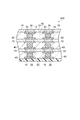
図1は、半導体装置の実施形態(半導体チップ及び基板のCOB型の接続態様)を示す模式断面図である。図1(a)に示すように、第1の半導体装置100は、互いに対向する半導体チップ10及び基板(回路配線基板)20と、半導体チップ10及び基板20の互いに対向する面にそれぞれ配置された配線15と、半導体チップ10及び基板20の配線15を互いに接続する接続バンプ30と、半導体チップ10及び基板20間の空隙に隙間なく充填された接着剤40とを有している。半導体チップ10及び基板20は、配線15及び接続バンプ30によりフリップチップ接続されている。配線15及び接続バンプ30は、接着剤40により封止されており外部環境から遮断されている。
FIG. 1 is a schematic cross-sectional view showing an embodiment of a semiconductor device (COB type connection mode between a semiconductor chip and a substrate). As shown in FIG. 1A, the
図1(b)に示すように、第2の半導体装置200は、互いに対向する半導体チップ10及び基板20と、半導体チップ10及び基板20の互いに対向する面にそれぞれ配置されたバンプ32と、半導体チップ10及び基板20間の空隙に隙間なく充填された接着剤40とを有している。半導体チップ10及び基板20は、対向するバンプ32が互いに接続されることによりフリップチップ接続されている。バンプ32は、接着剤40により封止されており外部環境から遮断されている。
As shown in FIG. 1B, the
図2は、半導体装置の他の実施形態(半導体チップ同士のCOC型の接続態様)を示す模式断面図である。図2(a)に示すように、第3の半導体装置300は、2つの半導体チップ10が配線15及び接続バンプ30によりフリップチップ接続されている点を除き、第1の半導体装置100と同様である。図2(b)に示すように、第4の半導体装置400は、2つの半導体チップ10がバンプ32によりフリップチップ接続されている点を除き、第2の半導体装置200と同様である。
FIG. 2 is a schematic cross-sectional view showing another embodiment of a semiconductor device (COC type connection mode between semiconductor chips). As shown in FIG. 2A, the
半導体チップ10としては、特に制限はなく、シリコン、ゲルマニウム等の同一種類の元素から構成される元素半導体、ガリウムヒ素、インジウムリン等の化合物半導体などの各種半導体を用いることができる。
There is no restriction | limiting in particular as the
基板20としては、配線回路基板であれば特に制限はなく、ガラスエポキシ、ポリイミド、ポリエステル、セラミック、エポキシ、ビスマレイミドトリアジン等を主な成分とする絶縁基板の表面に形成された金属層の不要な個所をエッチング除去して配線(配線パターン)が形成された回路基板、上記絶縁基板の表面に金属めっき等によって配線(配線パターン)が形成された回路基板、上記絶縁基板の表面に導電性物質を印刷して配線(配線パターン)が形成された回路基板などを用いることができる。
The
配線15、バンプ32等の接続部は、主成分として金、銀、銅、はんだ(主成分は、例えばスズ−銀、スズ−鉛、スズ−ビスマス、スズ−銅)、ニッケル、スズ、鉛等を含有しており、複数の金属を含有していてもよい。
The connection parts such as the
配線(配線パターン)の表面には、金、銀、銅、はんだ(主成分は、例えばスズ−銀、スズ−鉛、スズ−ビスマス、スズ−銅)、スズ、ニッケル等を主な成分とする金属層が形成されていてもよい。この金属層は単一の成分のみで構成されていてもよく、複数の成分から構成されていてもよい。また、複数の金属層が積層された構造をしていてもよい。銅、はんだは安価であることから一般的に使用されている。 The surface of the wiring (wiring pattern) is mainly composed of gold, silver, copper, solder (main components are, for example, tin-silver, tin-lead, tin-bismuth, tin-copper), tin, nickel, or the like. A metal layer may be formed. This metal layer may be composed of only a single component or may be composed of a plurality of components. Moreover, you may have the structure where the some metal layer was laminated | stacked. Copper and solder are generally used because they are inexpensive.
バンプと呼ばれる導電性突起の材質としては、主な成分として、金、銀、銅、はんだ(主成分は例えば、スズ−銀、スズ−鉛、スズ−ビスマス、スズ−銅)、スズ、ニッケル等が用いられ、単一の成分のみで構成されていてもよく、複数の成分から構成されていてもよい。また、これらの金属が積層された構造をなすように形成されていてもよい。バンプは半導体チップ又は基板に形成されていてもよい。銅、はんだは安価であることから一般的に使用されている。 As materials for the conductive protrusions called bumps, the main components are gold, silver, copper, solder (main components are, for example, tin-silver, tin-lead, tin-bismuth, tin-copper), tin, nickel, etc. May be used, and may be composed of only a single component or may be composed of a plurality of components. Moreover, you may form so that the structure where these metals were laminated | stacked may be made | formed. The bump may be formed on a semiconductor chip or a substrate. Copper and solder are generally used because they are inexpensive.
また、図1又は図2に示すような半導体装置(パッケージ)を積層して金、銀、銅、はんだ(主成分は、例えばスズ−銀、スズ−鉛、スズ−ビスマス、スズ−銅)、スズ、ニッケル等で電気的に接続してもよい。銅、はんだは安価であることから一般的に使用されているため好ましい。例えば、TSV技術で見られるような、接着剤を半導体チップ間に介して、フリップチップ接続又は積層し、半導体チップを貫通する孔を形成し、パターン面の電極とつなげてもよい。 Also, a semiconductor device (package) as shown in FIG. 1 or FIG. 2 is laminated and gold, silver, copper, solder (main components are, for example, tin-silver, tin-lead, tin-bismuth, tin-copper), You may electrically connect with tin, nickel, etc. Copper and solder are preferred because they are generally used because they are inexpensive. For example, as seen in the TSV technology, an adhesive may be flip-chip connected or stacked between semiconductor chips to form a hole penetrating the semiconductor chip and connected to the electrode on the pattern surface.
図3は、半導体装置の他の実施形態(半導体チップ積層型の態様(TSV))を示す模式断面図である。図3に示すように、第5の半導体装置500では、インターポーザ50上に形成された配線15が半導体チップ10の配線15と接続バンプ30を介して接続されることにより、半導体チップ10とインターポーザ50とはフリップチップ接続されている。半導体チップ10とインターポーザ50との間の空隙には接着剤40が隙間なく充填されている。上記半導体チップ10におけるインターポーザ50と反対側の表面上には、配線15、接続バンプ30及び接着剤40を介して半導体チップ10が繰り返し積層されている。半導体チップ10の表裏におけるパターン面の配線15は、半導体チップ10の内部を貫通する孔内に充填された貫通電極34により互いに接続されている。なお、貫通電極34の材質としては、銅、アルミニウム等を用いることができる。
FIG. 3 is a schematic cross-sectional view showing another embodiment of the semiconductor device (semiconductor chip laminated type (TSV)). As shown in FIG. 3, in the
このようなTSV技術により、通常は使用されない半導体チップの裏面からも信号を取得することができる。更には、半導体チップ10内に貫通電極34を垂直に通すため、対向する半導体チップ10間、又は半導体チップ10及びインターポーザ50間の距離を短くし、柔軟な接続が可能である。本実施形態に係る接着剤は、このようなTSV技術において、対向する半導体チップ10間、又は半導体チップ10及びインターポーザ50間の封止材料として好適に用いられる。
With such TSV technology, a signal can be obtained from the back surface of a semiconductor chip that is not normally used. Furthermore, since the through
また、エリアバンプチップ技術等の自由度の高いバンプ形成方法では、インターポーザを介さないでそのまま半導体チップをマザーボードに直接実装できる。本実施形態に係る接着剤は、このような半導体チップをマザーボードに直接実装する場合にも好適に用いられる。なお、本実施形態に係る接着剤は、2つの配線回路基板を積層する場合に、基板間の空隙を封止する際に好適に用いられる。 Further, in a bump forming method with a high degree of freedom such as area bump chip technology, a semiconductor chip can be directly mounted on a mother board without using an interposer. The adhesive according to this embodiment is also suitably used when such a semiconductor chip is directly mounted on a mother board. Note that the adhesive according to the present embodiment is suitably used when sealing the gap between the substrates when two printed circuit boards are stacked.
本実施形態に係る半導体装置の製造方法は、本実施形態に係る接着剤を用いて、半導体チップ及び配線回路基板、又は、複数の半導体チップ同士を接続する。本実施形態に係る半導体装置の製造方法は、例えば、接着剤を介して半導体チップ及び配線回路基板を互いに接続すると共に半導体チップ及び配線回路基板のそれぞれの接続部を互いに電気的に接続して半導体装置を得る工程、又は、接着剤を介して複数の半導体チップを互いに接続すると共に複数の半導体チップのそれぞれの接続部を互いに電気的に接続して半導体装置を得る工程を備える。 The method for manufacturing a semiconductor device according to the present embodiment connects a semiconductor chip and a printed circuit board, or a plurality of semiconductor chips using the adhesive according to the present embodiment. In the semiconductor device manufacturing method according to the present embodiment, for example, the semiconductor chip and the printed circuit board are connected to each other via an adhesive, and the connection portions of the semiconductor chip and the printed circuit board are electrically connected to each other. A step of obtaining a device, or a step of connecting a plurality of semiconductor chips to each other via an adhesive and electrically connecting respective connecting portions of the plurality of semiconductor chips to each other to obtain a semiconductor device.
本実施形態に係る半導体装置の製造方法では、接続部を互いに金属接合によって接続することができる。すなわち、半導体チップ及び配線回路基板のそれぞれの接続部を互いに金属接合によって接続する、又は、複数の半導体チップのそれぞれの接続部を互いに金属接合によって接続する。 In the method for manufacturing a semiconductor device according to the present embodiment, the connection portions can be connected to each other by metal bonding. That is, the connection portions of the semiconductor chip and the printed circuit board are connected to each other by metal bonding, or the connection portions of the plurality of semiconductor chips are connected to each other by metal bonding.
本実施形態に係る半導体装置の製造方法の一例として、図4に示す第6の半導体装置600の製造方法について説明する。第6の半導体装置600は、配線(銅配線)15を有する基板(例えばガラスエポキシ基板)60と、配線(例えば銅ピラー、銅ポスト)15を有する半導体チップ10とが接着剤40を介して互いに接続されている。半導体チップ10の配線15と基板60の配線15とは、接続バンプ(はんだバンプ)30により電気的に接続されている。基板60における配線15が形成された表面には、接続バンプ30の形成位置を除いてソルダーレジスト70が配置されている。
As an example of the method for manufacturing the semiconductor device according to this embodiment, a method for manufacturing the
第6の半導体装置600の製造方法では、まず、ソルダーレジスト70が形成された基板60上に接着剤(フィルム状接着剤等)40を貼付する。貼付は、加熱プレス、ロールラミネート、真空ラミネート等によって行うことができる。接着剤40の供給面積及び厚みは、半導体チップ10又は基板60のサイズ、バンプ高さ等によって適宜設定される。接着剤40を半導体チップ10に貼付してもよく、半導体ウエハに接着剤40を貼付した後にダイシングして半導体チップ10に個片化することによって、接着剤40を貼付した半導体チップ10を作製してもよい。接着剤40を基板60又は半導体チップ10に貼り付けた後、半導体チップ10の配線15上の接続バンプ30と、基板60の配線15とをフリップチップボンダー等の接続装置を用いて位置合わせする。そして、半導体チップ10と基板60を接続バンプ30の融点以上の温度で加熱しながら押し付けて(接続部にはんだを用いる場合は、はんだ部分に240℃以上かかることが好ましい)、半導体チップ10と基板60を接続すると共に、接着剤40によって半導体チップ10と基板60の間の空隙を封止充てんする。接続荷重は、バンプ数に依存するが、バンプの高さばらつき吸収、バンプ変形量の制御等を考慮して設定される。接続時間は、生産性向上の観点から、短時間が好ましい。はんだを溶融させ、酸化膜、表面の不純物等を除去し、金属接合を接続部に形成することが好ましい。
In the sixth method for manufacturing a
短時間の接続時間(圧着時間)とは、接続形成(本圧着)中に接続部に240℃以上かかる時間(例えば、はんだ使用時の時間)が4秒以下であることをいう。接続時間は、3秒以下が好ましい。 The short connection time (crimping time) means that the time required for 240 ° C. or more (for example, time when using solder) is 4 seconds or less during connection formation (final crimping). The connection time is preferably 3 seconds or less.
位置合わせをした後、仮固定して、リフロ炉で加熱処理することによってはんだバンプを溶融させて半導体チップと基板を接続することによって半導体装置を製造してもよい。仮固定は、金属接合を形成する必要性が顕著に要求されないため、上述の本圧着に比べて低荷重、短時間、低温度でもよく、生産性向上、接続部の劣化防止等のメリットが生じる。半導体チップと基板を接続した後、オーブン等で加熱処理を行って、接着剤を硬化させてもよい。加熱温度は、接着剤の硬化が進行し、好ましくは完全に硬化する温度である。加熱温度及び加熱時間は適宜設定すればよい。この場合、得られる半導体装置は、接着剤の硬化物を備える。 After the alignment, the semiconductor device may be manufactured by temporarily fixing, melting the solder bumps by heat treatment in a reflow furnace, and connecting the semiconductor chip and the substrate. Temporary fixing does not require the necessity of forming a metal bond, so it can have lower load, shorter time, and lower temperature than the above-mentioned main pressure bonding, and there are merits such as improvement of productivity and prevention of deterioration of connection parts. . After the semiconductor chip and the substrate are connected, the adhesive may be cured by performing a heat treatment in an oven or the like. The heating temperature is a temperature at which the curing of the adhesive proceeds, preferably complete curing. The heating temperature and the heating time may be set as appropriate. In this case, the obtained semiconductor device includes a cured product of the adhesive.
以下、実施例を用いて本発明を更に具体的に説明するが、本発明は実施例に限定されるものではない。 Hereinafter, the present invention will be described more specifically with reference to examples. However, the present invention is not limited to the examples.
(実施例1〜3及び比較例1〜3)
以下に示す成分を表1に示す配合で用い、下記の方法に従ってフィルム状接着剤を作製した。また、得られたフィルム状接着剤について、下記の方法に従って各特性を評価した。結果を表1に示す。
(Examples 1-3 and Comparative Examples 1-3)
Using the components shown below in the formulation shown in Table 1, a film adhesive was prepared according to the following method. Moreover, each characteristic was evaluated in accordance with the following method about the obtained film adhesive. The results are shown in Table 1.
・(a)成分:フルオレン骨格含有アクリレート(大阪ガスケミカル株式会社製、EA0200、2官能基)
・(b)成分:ジクミル過酸化物(日油株式会社製、パークミルD)
・(c)成分:
(c−1):3−メタクリロキシプロピルトリメトキシシラン(東レダウコーニング株式会社製、Z−6030)
(c−2):3−メタクリロキシプロピルトリメトキシシラン(信越化学工業株式会社製、KBM−503)
(c−3):3−メタクリロキシプロピルメチルジメトキシシラン(信越化学工業株式会社製、KBM−502)
・その他のカップリング剤
(x−1):3−メタクリロキシプロピルトリエトキシキシシラン(信越化学工業株式会社製、KBE−503)
(x−2):3−グリシドキシプロピルトリメトキシシラン(東レダウコーニング株式会社製、Z−6040)
・(d)成分:アクリルゴム(日立化成株式会社製、KH−CT865、Tg:0〜12℃、重量平均分子量:450000〜650000)
・フィラー
(e−1):シリカフィラー(株式会社アドマテックス製、SE2050、平均粒径0.5μm)
(e−2):メタクリル表面処理ナノシリカフィラー(株式会社アドマテックス製、YA050C−SM、以下SMナノシリカ とする、平均粒径約50nm)
(e−3):有機フィラー(ロームアンドハースジャパン(株)製、EXL−2655:コアシェルタイプ有機微粒子)
Component (a): fluorene skeleton-containing acrylate (Osaka Gas Chemical Co., Ltd., EA0200, bifunctional group)
-Component (b): Dicumyl peroxide (manufactured by NOF Corporation, Park Mill D)
-(C) component:
(C-1): 3-methacryloxypropyltrimethoxysilane (manufactured by Toray Dow Corning Co., Ltd., Z-6030)
(C-2): 3-methacryloxypropyltrimethoxysilane (manufactured by Shin-Etsu Chemical Co., Ltd., KBM-503)
(C-3): 3-methacryloxypropylmethyldimethoxysilane (manufactured by Shin-Etsu Chemical Co., Ltd., KBM-502)
Other coupling agent (x-1): 3-methacryloxypropyltriethoxyxysilane (manufactured by Shin-Etsu Chemical Co., Ltd., KBE-503)
(X-2): 3-glycidoxypropyltrimethoxysilane (manufactured by Toray Dow Corning Co., Ltd., Z-6040)
Component (d): Acrylic rubber (manufactured by Hitachi Chemical Co., Ltd., KH-CT865, Tg: 0 to 12 ° C., weight average molecular weight: 450,000 to 650000)
Filler (e-1): Silica filler (manufactured by Admatechs, SE2050, average particle size 0.5 μm)
(E-2): Methacrylic surface-treated nano silica filler (manufactured by Admatechs Co., Ltd., YA050C-SM, hereinafter referred to as SM nano silica, average particle diameter of about 50 nm)
(E-3): Organic filler (Rohm and Haas Japan Co., Ltd., EXL-2655: Core-shell type organic fine particles)
(フィルム状接着剤の作製方法)
(a)成分、(c)成分、及びフィラーをNV60質量%になるように有機溶媒(メチルエチルケトン)を添加した。その後、φ1.0mm、φ2.0mmのビーズを固形分と同質量加え、ビーズミル(フリッチュ・ジャパン株式会社製、遊星型微粉砕機P−7)で30分撹拌した。その後、(d)成分を加え、再度、ビーズミルで30分撹拌した。撹拌後、(b)成分を添加して攪拌した後、用いたビーズをろ過によって除去した。作製したワニスを小型精密塗工装置(廉井精機)で塗工し、クリーンオーブン(ESPEC製)で乾燥(70℃/10min)し、フィルム状接着剤を得た。
(Method for producing film adhesive)
An organic solvent (methyl ethyl ketone) was added so that the component (a), the component (c), and the filler were
(1)接着力評価(吸湿後260℃接着力測定)
フィルム状接着剤を切り抜き(5mm×5mm×0.045mmt)、上側シリコンチップ(5mm×5mm×0.725mmt、窒化膜コーティング)に80℃で貼付け、熱圧着試験機(日立化成テクノプラント株式会社製)を用いて下側シリコンチップ(10mm×8mm×0.725mmt、窒化膜コーティング)に圧着した(圧着条件:130℃/1s+250℃/4s、0.5MPa)。次に、クリーンオーブン(ESPEC製)中でアフターキュアした(175℃/2h)。その後、85℃/60%の恒温恒湿器(ESPEC製、PR−2KP)に48h放置し、取り出し後、260℃のホットプレート上で接着力測定装置(DAGE社製、万能型ボンドテスタDAGE4000型)を使い、基板からのツール高さ0.05mm、ツール速度0.05mm/sの条件で接着力を測定した。接着力が15kg以上の場合をA、10kg以上15kg未満の場合をB、5kg以上10kg未満の場合をC、5kg未満の場合をDとし評価し、A及びBを良好、C及びDを不良と判断した。
(1) Adhesive strength evaluation (260 ° C adhesive strength measurement after moisture absorption)
Cut out the film adhesive (5mm x 5mm x 0.045mm t ), paste it on the upper silicon chip (5mm x 5mm x 0.725mm t , nitride film coating) at 80 ° C, thermocompression testing machine (Hitachi Chemical Techno Plant Co., Ltd.) The product was pressure-bonded to a lower silicon chip (10 mm × 8 mm × 0.725 mm t , nitride film coating) using a company (compression condition: 130 ° C./1 s + 250 ° C./4 s, 0.5 MPa). Next, it was after-cured in a clean oven (manufactured by ESPEC) (175 ° C./2 h). Then, it is left for 48 hours in an 85 ° C./60% constant temperature and humidity chamber (manufactured by ESPEC, PR-2KP), taken out, and then taken out on a hot plate at 260 ° C. (adhesive bond tester DAGE 4000 type, manufactured by DAGE). Was used to measure the adhesive force under the conditions of a tool height of 0.05 mm from the substrate and a tool speed of 0.05 mm / s. The case where the adhesive strength is 15 kg or more is evaluated as A, the case where it is 10 kg or more and less than 15 kg is B, the case where it is 5 kg or more and less than 10 kg is C, and the case where it is less than 5 kg is evaluated as D. It was judged.
(2)半導体装置の製造方法
作製したフィルム状接着剤を切り抜き(8mm×8mm×0.045mmt)、ソルダーレジスト(太陽インキ社製、AUS308)を有するガラスエポキシ基板(ガラスエポキシ基材:420μm厚、銅配線:9μm厚、ピッチ80um、Cu配線とCu配線の間隔は40μm)上に真空ラミネーター(ニッコー・マテリアルズ株式会社製、V130)を用いて80℃/60sで貼付し、はんだバンプ付き半導体チップ(チップサイズ:7.3mm×7.3mm×0.15mmt、バンプ高さ:銅ピラー+はんだ計約45μm、バンプ数328、窒化膜コーティング)をFCB3(パナソニック製)で実装し(実装条件:圧着ヘッド温度130℃/1s+250℃/4s、75N)、図4に記載の半導体装置と同様の構造を有する半導体装置を得た。圧着する際に基板を置くFCB3内のステージの温度は80℃とした。
(2) Manufacturing method of semiconductor device The produced film adhesive was cut out (8 mm × 8 mm × 0.045 mm t ), and a glass epoxy substrate (glass epoxy substrate: 420 μm thickness) having a solder resist (Taiyo Ink Co., Ltd., AUS308) Copper wiring: 9 μm thickness, pitch 80 μm, Cu wiring and Cu wiring spacing is 40 μm) Using a vacuum laminator (Nikko Materials Co., Ltd., V130), paste at 80 ° C./60 s, semiconductor with solder bumps A chip (chip size: 7.3 mm × 7.3 mm × 0.15 mm t , bump height: copper pillar + solder meter about 45 μm, number of bumps 328, nitride coating) is mounted with FCB3 (manufactured by Panasonic) (mounting conditions) : Pressure head temperature 130 ° C./1 s + 250 ° C./4 s, 75 N), same as the semiconductor device shown in FIG. To obtain a semiconductor device having a structure. The temperature of the stage in the FCB 3 on which the substrate was placed during the pressure bonding was 80 ° C.
(3)ボイド評価
上記の圧着後のサンプルを、超音波映像診断装置(Insight−300、インサイト製)により、外観画像を撮り、スキャナGT−9300UF(EPSON社製)でチップ上の半導体接着剤層の画像を取り込み、画像処理ソフトAdobe Photoshopを用いて、色調補正、二階調化によりボイド部分を識別し、ヒストグラムによりボイド部分の占める割合を算出した。チップ上の半導体接着剤部分の面積を100%とした。ボイド発生率が10%以下の場合をA(良好)、ボイド発生率が10%を超える場合をB(不良)と評価した。
(3) Evaluation of voids The sample after crimping was taken with an ultrasonic diagnostic imaging apparatus (Insight-300, manufactured by Insight), and an external image was taken. The image of the layer was taken in, and the void portion was identified by color tone correction and two-gradation using the image processing software Adobe Photoshop, and the ratio of the void portion was calculated by the histogram. The area of the semiconductor adhesive portion on the chip was 100%. The case where the void generation rate was 10% or less was evaluated as A (good), and the case where the void generation rate exceeded 10% was evaluated as B (defective).
(4)接続評価
上記ガラスエポキシ基板とはんだバンプ付き半導体チップ(デイジーチェーン接続)をFCB3で実装後にマルチメータ(ADVANTEST製、R6871E)を用いて初期導通の可否を測定した。初期接続抵抗値が10.0〜15Ωの場合をA(接続良好)、それ以外の場合をB(接続不良)と評価した。
(4) Connection evaluation After mounting the glass epoxy substrate and the semiconductor chip with solder bumps (daisy chain connection) on FCB3, the possibility of initial conduction was measured using a multimeter (manufactured by ADVANTEST, R6871E). The case where the initial connection resistance value was 10.0 to 15Ω was evaluated as A (good connection), and the other cases were evaluated as B (connection failure).
(5)耐リフロ性評価
(2)で作製したパッケージを、封止材(日立化成製、CEL9750ZHF10)を用いてモールドした(条件:180℃/6.75MPa/90s)。次に、クリーンオーブン(ESPEC製)中で175℃、5時間アフターキュアを行った。その後、JEDEC level 2条件で高温吸湿後、リフロ(FURUKAWA ELECTRIC製、SALAMANDER)評価(リフロ炉を3回通した)を行った。リフロ後、剥離なく、接続良好なサンプルをA、剥離、接続不良が生じたサンプルをBと評価した。接続評価は、(4)と同様な方法で行った。
(5) Evaluation of reflow resistance The package prepared in (2) was molded using a sealing material (CEL9750ZHF10, manufactured by Hitachi Chemical Co., Ltd.) (condition: 180 ° C./6.75 MPa / 90 s). Next, after-curing was performed at 175 ° C. for 5 hours in a clean oven (manufactured by ESPEC). Then, after high-temperature moisture absorption under JEDEC level 2, conditions for reflow (manufactured by FURUKAWA ELECTRIC, SALAMANDER) were evaluated (reflow furnace was passed 3 times). After reflow, a sample with good connection without peeling was evaluated as A, and a sample with peeling and poor connection was evaluated as B. Connection evaluation was performed in the same manner as in (4).
10…半導体チップ、15…配線、20,60…基板、30…接続バンプ、32…バンプ、34…貫通電極、40…接着剤、50…インターポーザ、70…ソルダーレジスト、100,200,300,400,500,600…半導体装置。
DESCRIPTION OF
Claims (10)
[式(1)中、R1は水素原子、メチル基又はエチル基を表し、R2、R3及びR4は、それぞれ独立に水素原子、−(CH2)m−CH3で表されるアルキル基、又はアルコキシ基を表し、かつR2、R3及びR4の少なくとも一つはメトキシ基を表し、mは0〜3の整数を表し、nは1〜6の整数を表す。] The adhesive for semiconductors containing a (meth) acrylic compound, a hardening | curing agent, and the compound represented by following formula (1).
In Expression (1), R 1 represents a hydrogen atom, a methyl group or an ethyl group, R 2, R 3 and R 4 are each independently a hydrogen atom, - represented by (CH 2) m -CH 3 It represents an alkyl group or an alkoxy group, and at least one of R 2 , R 3 and R 4 represents a methoxy group, m represents an integer of 0 to 3, and n represents an integer of 1 to 6. ]
Priority Applications (1)
| Application Number | Priority Date | Filing Date | Title |
|---|---|---|---|
| JP2015233900A JP2017103303A (en) | 2015-11-30 | 2015-11-30 | Adhesive for semiconductor, semiconductor device, and method for manufacturing the same |
Applications Claiming Priority (1)
| Application Number | Priority Date | Filing Date | Title |
|---|---|---|---|
| JP2015233900A JP2017103303A (en) | 2015-11-30 | 2015-11-30 | Adhesive for semiconductor, semiconductor device, and method for manufacturing the same |
Publications (1)
| Publication Number | Publication Date |
|---|---|
| JP2017103303A true JP2017103303A (en) | 2017-06-08 |
Family
ID=59015702
Family Applications (1)
| Application Number | Title | Priority Date | Filing Date |
|---|---|---|---|
| JP2015233900A Pending JP2017103303A (en) | 2015-11-30 | 2015-11-30 | Adhesive for semiconductor, semiconductor device, and method for manufacturing the same |
Country Status (1)
| Country | Link |
|---|---|
| JP (1) | JP2017103303A (en) |
Citations (4)
| Publication number | Priority date | Publication date | Assignee | Title |
|---|---|---|---|---|
| US20070213467A1 (en) * | 2004-03-19 | 2007-09-13 | Hikaru Okubo | Resin Composition and Semiconductor Device Produced By Using the Same |
| JP2012041541A (en) * | 2011-09-21 | 2012-03-01 | Sony Chemical & Information Device Corp | Circuit connecting material, connecting method using the same, and connection structure |
| WO2013161713A1 (en) * | 2012-04-25 | 2013-10-31 | 日立化成株式会社 | Circuit connection material, circuit connection structure, adhesive film, and wound body |
| JP2015172145A (en) * | 2014-03-12 | 2015-10-01 | ナミックス株式会社 | Resin composition, prior supply type semiconductor sealant, semiconductor sealing film, and semiconductor device |
-
2015
- 2015-11-30 JP JP2015233900A patent/JP2017103303A/en active Pending
Patent Citations (4)
| Publication number | Priority date | Publication date | Assignee | Title |
|---|---|---|---|---|
| US20070213467A1 (en) * | 2004-03-19 | 2007-09-13 | Hikaru Okubo | Resin Composition and Semiconductor Device Produced By Using the Same |
| JP2012041541A (en) * | 2011-09-21 | 2012-03-01 | Sony Chemical & Information Device Corp | Circuit connecting material, connecting method using the same, and connection structure |
| WO2013161713A1 (en) * | 2012-04-25 | 2013-10-31 | 日立化成株式会社 | Circuit connection material, circuit connection structure, adhesive film, and wound body |
| JP2015172145A (en) * | 2014-03-12 | 2015-10-01 | ナミックス株式会社 | Resin composition, prior supply type semiconductor sealant, semiconductor sealing film, and semiconductor device |
Similar Documents
| Publication | Publication Date | Title |
|---|---|---|
| US11608455B2 (en) | Adhesive for semiconductor device, and high productivity method for manufacturing said device | |
| JP6477971B2 (en) | Manufacturing method of semiconductor device | |
| JP2017220519A (en) | Semiconductor device manufacturing method | |
| JP2017045891A (en) | Semiconductor device and method of manufacturing the same | |
| JP2019137866A (en) | Adhesive for semiconductor, semiconductor device, and manufacturing method therefor | |
| TWI827512B (en) | Film adhesive for semiconductors, manufacturing method of semiconductor device, and semiconductor device | |
| JP2017122193A (en) | Semiconductor adhesive and method for producing semiconductor device | |
| JP6859708B2 (en) | How to manufacture semiconductor devices | |
| JP6544146B2 (en) | Semiconductor device and method of manufacturing the same | |
| WO2020196430A1 (en) | Adhesive agent for semiconductor, method for producing semiconductor device, and semiconductor device | |
| JP2017171817A (en) | Adhesive for semiconductor, semiconductor device and method for manufacturing semiconductor device | |
| JP2017041499A (en) | Adhesive for semiconductor, and semiconductor device and method for manufacturing the same | |
| JP6690308B2 (en) | Method for manufacturing semiconductor device | |
| TW202018048A (en) | Adhesive composition and semiconductor device production method | |
| JP2017103289A (en) | Adhesive for semiconductor, semiconductor device, and method for manufacturing the same | |
| JP2017103303A (en) | Adhesive for semiconductor, semiconductor device, and method for manufacturing the same | |
| JP2017103304A (en) | Adhesive for semiconductor, semiconductor device, and method for manufacturing the same | |
| JP2017203138A (en) | Adhesive for semiconductor, semiconductor device and manufacturing method therefor | |
| TWI834852B (en) | Adhesive for semiconductors, manufacturing method of semiconductor device, and semiconductor device | |
| JP2017218532A (en) | Semiconductor adhesive, semiconductor device, and method for producing semiconductor device | |
| JP2022043572A (en) | Semiconductor device manufacturing method |
Legal Events
| Date | Code | Title | Description |
|---|---|---|---|
| A621 | Written request for application examination |
Free format text: JAPANESE INTERMEDIATE CODE: A621 Effective date: 20181001 |
|
| A977 | Report on retrieval |
Free format text: JAPANESE INTERMEDIATE CODE: A971007 Effective date: 20190624 |
|
| A131 | Notification of reasons for refusal |
Free format text: JAPANESE INTERMEDIATE CODE: A131 Effective date: 20190723 |
|
| A02 | Decision of refusal |
Free format text: JAPANESE INTERMEDIATE CODE: A02 Effective date: 20200218 |