JP2017007459A - Transmitter for track circuit - Google Patents
Transmitter for track circuit Download PDFInfo
- Publication number
- JP2017007459A JP2017007459A JP2015123686A JP2015123686A JP2017007459A JP 2017007459 A JP2017007459 A JP 2017007459A JP 2015123686 A JP2015123686 A JP 2015123686A JP 2015123686 A JP2015123686 A JP 2015123686A JP 2017007459 A JP2017007459 A JP 2017007459A
- Authority
- JP
- Japan
- Prior art keywords
- signal
- output
- level
- track circuit
- circuit
- Prior art date
- Legal status (The legal status is an assumption and is not a legal conclusion. Google has not performed a legal analysis and makes no representation as to the accuracy of the status listed.)
- Granted
Links
Images


Abstract
Description
本発明は、軌道回路用送信器に関し、特に鉄道用保安装置のひとつである自動列車制御装置において用いられる2重系の軌道回路用送信器に適用して好適なものである。 The present invention relates to a track circuit transmitter, and is particularly suitable for application to a dual track circuit transmitter used in an automatic train control device which is one of railway security devices.
一般に自動列車制御装置は、ATC(Automatic Train Control)装置と呼ばれる。ATC装置は、地上装置、軌道回路及び車上装置等から構成される。地上装置は、先行列車との間隔や進路の開通状況等に基づいて、対象列車の停止限界位置を決定し、停止限界位置の情報を含む列車制御信号(ATC信号)を生成して軌道回路に送信する。 Generally, the automatic train control device is called an ATC (Automatic Train Control) device. The ATC device includes a ground device, a track circuit, an on-vehicle device, and the like. The ground device determines the stop limit position of the target train based on the distance from the preceding train, the route opening situation, etc., and generates a train control signal (ATC signal) including information on the stop limit position to the track circuit. Send.
対象列車に予め設置される車上装置は、軌道回路を介してATC信号を受信し、ATC信号に含まれる停止限界位置の情報に基づいて、対象列車を停止可能な速度に制御する。 The on-board device installed in advance in the target train receives the ATC signal via the track circuit, and controls the target train to a speed at which the target train can be stopped based on the information on the stop limit position included in the ATC signal.
ところで地上装置は、列車の在線位置を検知する論理部を備える。論理部は、列車の在線位置を検知する際、軌道回路への送信端に接続されている軌道回路用送信器を介して列車検知信号(TD信号)を軌道回路に送信する。 By the way, a ground apparatus is provided with the logic part which detects the existing position of a train. The logic unit transmits a train detection signal (TD signal) to the track circuit via the track circuit transmitter connected to the transmission end to the track circuit when detecting the train position.
そして論理部は、軌道回路の受信端に接続されている軌道回路用受信器によりTD信号を受信し、このTD信号に基づいて、軌道回路内に列車が在線するか否かを判断する。例えば論理部は、TD信号の信号レベルが規定値未満である場合に「在線」と判断する。 The logic unit receives the TD signal by the track circuit receiver connected to the receiving end of the track circuit, and determines whether or not the train is in the track circuit based on the TD signal. For example, the logic unit determines “present line” when the signal level of the TD signal is less than a specified value.
これに対し論理部は、TD信号の信号レベルが規定値以上である場合、安全性を確保するため即座に「非在線」とは判断せず、更に軌道回路用送信器により送信したTD信号の内容と、軌道回路用受信器により受信したTD信号の内容とが一致した場合に限り「非在線」と判断する。 On the other hand, when the signal level of the TD signal is equal to or higher than the specified value, the logic unit does not immediately determine “non-existing line” in order to ensure safety, and further, the TD signal transmitted by the track circuit transmitter. Only when the contents match the contents of the TD signal received by the track circuit receiver, it is determined that the line is not present.
軌道回路用送信器は、故障が発生した場合でも列車の運行に支障が生じないように送信器を2組備え、一方を使用系、他方を待機系として運用するいわゆる待機2重系の構成が採用される。軌道回路用送信器は、使用系に故障が発生した場合には待機系を使用系に切り替えるように動作する。 The track circuit transmitter has a so-called standby dual system configuration in which two sets of transmitters are provided so as not to hinder the train operation even when a failure occurs, and one is used as a standby system and the other as a standby system. Adopted. The track circuit transmitter operates to switch the standby system to the use system when a failure occurs in the use system.
ここで特許文献1には、待機2重系の構成が開示されている。具体的には2組の情報処理装置の出力側のそれぞれに切り替え手段を介して模擬負荷が接続されており、待機系の情報処理装置は使用系の情報処理装置と同様の処理を実行するとともに、処理結果は模擬負荷に送出される待機2重系の構成が開示されている。
Here,
また特許文献2には、使用系と待機系とを切り替える切り替え手段の構成が開示されている。具体的に制御部は、出力リレーを動作させる条件であるとき所定の交番周波数の交番信号を生成してリレー駆動部に出力し、リレー駆動部は、コンデンサを使用したチャージ・ポンプ回路からなり、制御部から入力する交番信号の交番周波数に応じてコンデンサの放電電流を可変して出力リレーのコイルを励磁させる構成が開示されている。
また特許文献3には、交番信号をフェールセーフに制御する構成が開示されている。具体的には、複数のフリップフロップを縦列に接続し、最後段のフリップフロップの出力を最前段の入力に反転させて結合したリングを構成し、各々のフリップフロップのタイミング(又はクロック)入力端子に論理回路としての信号を入力する構成が開示されている。
しかし特許文献2に記載のチャージ・ポンプ回路では、交番信号の入力が停止する場合、H(High)レベルで固定となるか、L(Low)レベルで固定となるかによって、放電対象のコンデンサが異なる。その結果、コンデンサの放電時間が異なる。
However, in the charge pump circuit described in
切り替えリレーを遮断する際、どちらの入力レベルで交番信号が停止するかによって、リレー駆動回路の出力が励磁状態から非励磁状態になるまでの時間(非励磁移行時間)が異なるという課題がある。 When the switching relay is cut off, there is a problem that the time (de-excitation transition time) until the output of the relay drive circuit changes from the excited state to the non-excited state differs depending on at which input level the alternating signal stops.
すなわち特許文献1に記載されている待機2重系の構成に特許文献2に記載されているチャージ・ポンプ回路を適用すると、軌道回路に信号を送信している間に使用系から待機系に遷移する際、交番信号を停止してから切り替えリレーが遮断するまでの時間が入力レベルによって異なる場合がある。
That is, when the charge pump circuit described in
ここで、切り替えリレーは動作状態で出力先を軌道回路に切り替え、復帰状態で出力先を模擬負荷に切り替える構成を想定し、模擬負荷に信号を出力する際には負荷抵抗の定格電力を考慮して軌道回路に出力する場合よりも電力を低減させて出力する必要がある。 Here, the switching relay assumes a configuration in which the output destination is switched to the track circuit in the operating state and the output destination is switched to the simulated load in the return state, and the rated power of the load resistance is taken into account when outputting a signal to the simulated load. Therefore, it is necessary to output with lower power than when outputting to the track circuit.
この場合、想定よりも早いタイミングで遮断すると、軌道回路に出力する電力を模擬負荷に出力して模擬負荷が故障する場合がある。これに対し、想定よりも遅いタイミングで遮断すると、2組の送信器が同時に使用系の状態となり出力信号同士が衝突し、例えば変調したデータが壊れたり、列車運行に支障が生じたりする場合がある。 In this case, if the power is interrupted at an earlier timing than expected, the power output to the track circuit may be output to the simulated load and the simulated load may fail. On the other hand, if the transmitter is shut off at a timing slower than expected, the two sets of transmitters may be in use at the same time, and the output signals may collide with each other, for example, the modulated data may be damaged or the train operation may be hindered. is there.
本発明は以上の点を考慮してなされたものであり、使用系と待機系とが入れ替わる際、交番信号の入力レベルが0又は1の何れで停止した場合であっても、非励磁移行時間を一律に固定し、軌道回路への送信制御を安定化し得る軌道回路用送信器を提案するものである。 The present invention has been made in consideration of the above points, and when the use system and the standby system are switched, even if the input level of the alternating signal is stopped at 0 or 1, the non-excitation transition time is reached. The track circuit transmitter is proposed that can stabilize the transmission uniformly and stabilize the transmission control to the track circuit.
かかる課題を解決するために、本発明においては、交番信号を生成して軌道回路に送信する2重系の軌道回路用送信器において、外部機器からの系切替指示に基づいて、交番信号、プリセット信号及びクリア信号を生成して出力する信号出力制御部と、信号出力制御部からの交番信号、プリセット信号及びクリア信号を入力して所定のタイミングで出力するタイミング調整器と、交番信号、プリセット信号及びクリア信号を入力し、プリセット信号及びクリア信号に基づいて、後段の機器に出力する出力信号の信号レベルを固定し、信号レベルを固定した出力信号を出力するフェールセーフ論理回路と、信号レベルが固定された出力信号に基づいて動作するリレー駆動回路と、リレー駆動回路の動作に基づいて、キャリア波生成器により生成されたキャリア波の出力先を軌道回路又は模擬負荷の何れかに切り替える切替リレーとを備えることを特徴とする。 In order to solve such a problem, in the present invention, in a dual-system track circuit transmitter that generates an alternating signal and transmits it to the track circuit, the alternating signal and the preset are set based on a system switching instruction from an external device. A signal output control unit that generates and outputs a signal and a clear signal, a timing adjuster that inputs an alternating signal, a preset signal, and a clear signal from the signal output control unit and outputs them at a predetermined timing, an alternating signal, and a preset signal A fail-safe logic circuit that inputs a clear signal, fixes a signal level of an output signal output to a subsequent device based on the preset signal and the clear signal, and outputs an output signal in which the signal level is fixed; Generated by the carrier wave generator based on the relay drive circuit that operates based on the fixed output signal and the operation of the relay drive circuit Characterized in that it comprises a switching relay for switching the carrier wave of the output destination to one of the track circuit or simulated load.
本発明によれば、待機2重系構成の軌道回路用送受信器において、使用系と待機系とが入れ替わる際、交番信号の入力レベルが0又は1の何れで停止した場合であっても、非励磁移行時間を一律に固定し、軌道回路への送信制御を安定化することができる。 According to the present invention, in a transceiver for a track circuit having a standby dual system configuration, when the active system and the standby system are switched, even if the input level of the alternating signal is stopped at either 0 or 1, The excitation transition time is fixed uniformly, and transmission control to the track circuit can be stabilized.
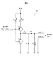
図1は、第1の実施の形態における軌道回路用送信器のブロック図を示す。軌道回路用送信器は、2組の送信器1及び28(1系及び2系)の待機2重系により構成される。
FIG. 1 is a block diagram of a track circuit transmitter according to the first embodiment. The track circuit transmitter includes two sets of
送信器1は、2組の信号出力制御部3A及び3B、2組のキャリア波生成器4A及び4B、2組の選択器6A及び6B、2組の変調器8A及び8B、2組のレベル調整器12A及び12B、2組のフィルタ13A及び13B、増幅器14、2組のタイミング調整器10A及び10B、フェールセーフ論理回路21、リレー駆動回路23、切替リレー25並びに模擬負荷27から構成される。
The
以下送信器1が備える各部の構成について説明する。なお送信器28の各部の構成は送信器1と同様であるため説明は省略する。
Hereinafter, the configuration of each unit included in the
信号出力制御部3Aは、ATC論理部2からの制御信号29に基づいてTD信号の出力制御を実行し、信号出力制御部3Bは、制御信号29に基づいてATC信号の出力制御を実行する。キャリア波生成器4Aは、TD信号用のキャリア波を生成し、キャリア波生成器4Bは、ATC信号用のキャリア波を生成する。
The signal output control unit 3A executes TD signal output control based on the
選択器6Aは、信号出力制御部3Aからの選択指示5Aに基づいて、キャリア波生成器4Aからのキャリア波を出力するか、或いは、未出力とするかを選択する。同様に選択器6Bは、信号出力制御部3Bからの選択指示5Bに基づいて、キャリア波生成器4Bからのキャリア波を出力するか、或いは、未出力とするかを選択する。
The
変調器8Aは、信号出力制御部3AからのTD信号の情報(TD情報)7Aに基づいて、キャリア波の周波数を変調する。一方で変調器8Bは、信号出力制御部3BからのATC信号の情報(ATC情報)7Bに基づいて、キャリア波の周波数を変調する。レベル調整器12Aは、信号出力制御部3Aからのレベル調整指示9Aをタイミング調整器10Aがタイミング調整したレベル指示11Aに基づいて、TD信号のレベルを調整する。
The
またレベル調整器12Bは、信号出力制御部3Bからのレベル調整指示9Bをタイミング調整器10Bがタイミング調整したレベル指示11Bに基づいて、ATC信号のレベルを調整する。フィルタ13Aは、レベル調整器12AからのTD信号に対して帯域制限をかけ、不要なノイズ成分をカットする。フィルタ13Bも同様にレベル調整器12BからのATC信号に対して帯域制限をかけ、不要なノイズ成分をカットする。
Further, the
増幅器14は、フィルタ13AからのTD信号又はフィルタ13BからのATC信号を増幅する。交番信号15A及び15B、プリセット信号16A及び16B並びにクリア信号17A及び17Bは、ATC論理部2からの系切替指示に基づいて、信号出力制御部3A及び3Bから出力される信号である。
The
交番信号18A及び18Bは、タイミング調整器10A及び10Bによりタイミング調整された信号である。プリセット信号19A及び19Bは、タイミング調整器10A及び10Bによりタイミングが調整された信号であり、フェールセーフ論理回路21をプリセットする信号である。クリア信号20A及び20Bは、タイミング調整器10A及び10Bによりタイミングが調整された信号であり、フェールセーフ論理回路21をクリアする信号である。
The alternating signals 18A and 18B are signals whose timings are adjusted by the timing
フェールセーフ論理回路21の詳細については後述する(図2及び図3)。リレー駆動回路23は、フェールセーフ論理回路21からの出力信号22に基づいて動作する。リレー駆動回路23の詳細については後述する(図4)。切替リレー25は、リレー駆動回路23からの出力信号24に基づいて、TD信号又はATC信号の出力先を軌道回路26又は模擬負荷27の何れかに切り替える。
Details of the fail-
以上が送信器1(送信器28)の構成である。ATC論理部2は、列車の在線を検知する際、軌道回路26にTD信号を出力し、また列車の速度を制御する際、軌道回路26にATC信号を出力する。TD信号の流れについて説明すると、ATC論理部2からTD信号の出力指示を入力した信号出力制御部3Aは、選択指示5Aを選択器6Aに出力し、TD情報7Aを変調器8Aに出力する。
The above is the configuration of the transmitter 1 (transmitter 28). The
レベル調整器12Aは出力レベルを指定のレベルに調整し、増幅器14は電力を増幅する。使用系の場合、信号出力制御部3Aは、交番信号15Aをフェールセーフ論理回路21に出力する。そしてリレー駆動回路23は、切替リレー25を励磁し、切替リレー25はTD信号を軌道回路26に出力する。
The
ATC信号についてもTD信号と同様、使用系の場合には最終的に切替リレー25がATC信号を軌道回路26に出力する。
Similarly to the TD signal, the switching
軌道回路用送信器は、例えば1日1回定期的な系切替動作を行う。或いは他系の故障に伴い系切替動作を行う。送信器1は、ATC論理部2から、使用系から待機系の系切換指示を受けると、信号出力制御部3A(3B)から出力している交番信号15A(15B)の入力を停止する。
The track circuit transmitter performs a periodic system switching operation once a day, for example. Alternatively, a system switching operation is performed in accordance with a failure of another system. When the
この結果、リレー駆動回路23からの出力信号24が非励磁になることに伴い、切替リレー25は復帰状態になる。そして切替リレー25は、出力先を軌道回路26から模擬負荷27に切り替える。
As a result, as the
図2は、本実施の形態におけるフェールセーフ論理回路21のブロック図を示す。また図3は、比較例として従来のフェールセーフ論理回路30のブロック図を示す。本実施の形態におけるフェールセーフ論理回路21は、従来のフェールセーフ論理回路30と比較して、プリセット機能及びクリア機能を備える。
FIG. 2 shows a block diagram of the fail-
具体的にフェールセーフ論理回路21は、2段のフリップフロップ33及び34を備え、信号出力制御部3A及び3Bからのプリセット信号Pa及びPb(19A及び19B)並びにクリア信号Ca及びCb(20A及び20B)に基づいて、切替リレー25が遮断する場合には必ず出力信号22をL(Low)又はH(High)に固定する。
Specifically, the fail-
より詳細には、フリップフロップ33及び34にはプリセット信号Pa及びPbを入力するプリセット(PRE)と、クリア信号Ca及びCbを入力するクリア(CLR)とを備える。交番信号Xa及びXb(18A及び18B)の入力が停止する場合、フェールセーフ論理回路21は、フリップフロップ33及び34をクリア状態(Pa及びPbをHレベルかつCa及びCbをLレベル)又はプリセット状態(Pa及びPbをLレベルかつCa及びCbをHレベル)にする。
More specifically, the flip-
これにより、交番信号Xa及びXbの状態(L又はH)にかかわらず、フェールセーフ論理回路21の出力信号Z(22)をL又はHに固定することができる。
Thereby, the output signal Z (22) of the fail
これに対し従来のフェールセーフ論理回路30では、ATC論理部2から待機系指示を入力すると、交番信号Xa及びXbの入力が停止する。待機系指示のタイミングと、交番信号Xa及びXbのタイミングは同期していないため、交番信号Xa及びXbの状態は、Lレベル又はHレベルの何れにもなり得る。この場合、出力信号Zの状態もLレベル又はHレベルの何れにもなり得る。
On the other hand, in the conventional
図4は、リレー駆動回路23の回路構成を示す。リレー駆動回路23の入力において、コンデンサC1とC2とが充電状態の場合、入力信号がHレベルに固定される場合には非励磁移行時間はC1とC2との放電時間となる。一方で入力信号がLレベルに固定される場合には非励磁移行時間はC2の放電時間のみとなる。
FIG. 4 shows a circuit configuration of the
以下リレー駆動回路23の動作について詳細に説明する。フェールセーフ論理回路21からの出力信号22(リレー駆動回路23が入力する入力信号)がLレベルである場合、リレー駆動回路23は、スイッチング素子T1をONにして、スイッチング素子T2をOFFにする。そしてコンデンサC1を充電する。
Hereinafter, the operation of the
一方でフェールセーフ論理回路21からの出力信号22がHレベルになると、リレー駆動回路23は、スイッチング素子T1をOFFにして、スイッチング素子T2をONにする。そしてコンデンサC1に充電されている電荷によりコンデンサC2を充電し、切替リレー25を励磁する。
On the other hand, when the
リレー駆動回路23が使用系の場合、フェールセーフ論理回路21からの出力信号22は交番信号になり、コンデンサC2を充電し、切替リレー25を励磁する。待機系に遷移するためには、フェールセーフ論理回路21からの出力信号22がLレベルである場合にはコンデンサC2が切替リレー25によって消費される時間を要する。
When the
またフェールセーフ論理回路21からの出力信号22がHレベルの場合には、コンデンサC1とC2とが切替リレー25によって消費される時間を要する。
When the
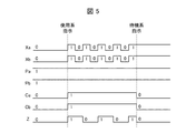
図5は、フェールセーフ論理回路21の動作タイミングを示す。フェールセーフ論理回路21は、ATC論理部2から待機系指示が出力された場合、交番信号Xa及びXbの入力を停止するとともに、フリップフロップ33及び34においてLレベルのクリア信号Ca及びCbを入力し、Hレベルのプリセット信号Pa及びPbを入力することにより、出力信号ZのレベルをLレベルに固定する。
FIG. 5 shows the operation timing of the fail-
その後にATC論理部2から使用系指示が出力された場合にはHレベルのプリセット信号Pa及びPb並びにクリア信号Ca及びCbを入力するとともに、交番信号Xa及びXbを入力する。
Thereafter, when a usage instruction is output from the
図6はフェールセーフ論理回路21の他の動作タイミングを示す。各フリップフロップ33及び34に対するプリセット信号Pa及びPb並びにクリア信号Ca及びCbの論理が逆になっている点で、図5の動作タイミングと異なる。すなわちここではフェールセーフ論理回路21からの出力信号ZのレベルはHレベルに固定される。
FIG. 6 shows another operation timing of the fail
なおここではフェールセーフ論理回路21は2段のフリップフロップ33及び34を備える構成について説明しているが、これに限らず、3段以上の多段のフリップフロップを備える構成であってもよい。
Here, the fail-
フェールセーフ論理回路21は、レベル調整器12A又は12Bが模擬負荷27向けにTD信号又はATC信号のレベルを下げる前に切替リレー25が即座に遮断した際に軌道回路26に向けた過大なレベルのTD信号又はATC信号を模擬負荷27に印加しないようにするため、従来の構成に加えて、プリセット機能及びクリア機能を備えている。
The fail-
これらレベル調整器12A,12Bは、既述の非励磁移行時間としてのC2(図4参照)の放電時間に合わせてレベル指示11A及び11Bの出力タイミングを決定することにより、模擬負荷27に対して過大なレベルのTD信号又はATC信号が印加されることを防止することができる。また1系2系の送信器1及び28から同時に軌道回路26に信号が出力されることを防止することができる。
These
待機系から使用系への遷移時についても同様である。すなわちリレー駆動回路23が非励磁から励磁に移行する時間(励磁移行時間)に合わせて、タイミング調整器10A及び10Bがレベル指示11A及び11Bの出力タイミングを調整し、模擬負荷27に対して過大なTD信号又はATC信号が印加されることを防止することができる。
The same applies to the transition from the standby system to the use system. That is, the timing
本実施の形態では、切替リレー25について励磁移行時間Tonと非励磁移行時間Toffとの関係によってタイミング調整器10A(10B)の挙動を変えるようにしている。具体的には、タイミング調整器10A(10B)は、励磁移行時間Tonと非励磁移行時間Toffとの関係に応じて後述のように制御する。
In the present embodiment, the behavior of the timing adjuster 10A (10B) is changed according to the relationship between the excitation transition time Ton and the non-excitation transition time Toff for the switching
図7及び図8は、使用系から待機系に遷移する場合におけるタイミング調整器10A(10B)の動作タイミングを示している。なお、図7(A)及び図8(A)は、それぞれ、軌道回路用送信器1のタイミング調整器10A(10B)の動作例を示している一方、図7(B)及び図8(B)は、それぞれ、軌道回路用送信器28のタイミング調整器10A(10B)の動作例を示している。
7 and 8 show the operation timing of the timing adjuster 10A (10B) when transitioning from the active system to the standby system. 7A and 8A show examples of the operation of the timing adjuster 10A (10B) of the
まず、タイミング調整器10A(10B)は、図7に示すようにTon>Toffの場合、待機系に遷移する際の調整時間を更に(Ton−Toff)分だけ遅らせる。一方、タイミング調整器10A(10B)は、図8に示すようにTon<Toffの場合、使用系に遷移する際の調整時間を更に(Toff−Ton)分だけ遅らせる。
First, as shown in FIG. 7, the
これにより、軌道回路26に対する出力が途切れることなく、送信器1又は28のうちの何れか一方により制御を行うことができる。
As a result, the output to the
図9及び図10は、第2の実施の形態として、使用系から待機系に遷移した場合におけるレベル調整器12A(12B)の動作タイミングを示す。また切替リレー25の非励磁移行時間をToff、フィルタ13A(13B)での遅延時間をTdelayとした場合、図9はToff>Tdelayの場合の動作タイミングを示し、図10はToff<Tdelayの場合の動作タイミングを示す。
FIG. 9 and FIG. 10 show the operation timing of the
第2の実施の形態におけるフェールセーフ論理回路21は、待機系の場合、Hレベル又はLレベルに固定した出力信号22を出力するため、切替リレー25の非励磁移行時間Toffを一律固定にすることができる。
In the case of the standby system, the fail-
Toff>Tdelayの場合、信号出力制御部3A(3B)から出力されたレベル調整指示9A(9B)をタイミング調整器10A(10B)によって(Toff−Tdelay)時間遅延させる。 When Toff> Tdelay, the level adjustment instruction 9A (9B) output from the signal output control unit 3A (3B) is delayed by (Toff-Tdelay) time by the timing adjuster 10A (10B).
Toff<Tdelayの場合、信号出力制御部3A(3B)から出力される交番信号15A(15B)、フェールセーフ論理回路21に対するプリセット信号16A(16B)及びクリア信号17A(17B)について、タイミング調整器10A(10B)によって(Tdelay−Toff)時間遅延させる。
In the case of Toff <Tdelay, the timing adjuster 10A for the alternating signal 15A (15B) output from the signal output control unit 3A (3B), the
また、フェールセーフ論理回路21へは、交番信号18A(18B)、フェールセーフ論理回路21に対するプリセット信号19A(19B)及びクリア信号20A(20B)を入力する。これにより、切替リレー25の復帰とレベルの調整とを同時に行うことができる。なおTdelay=Toffの場合は、タイミングを調整する必要はない。
Further, the alternating
待機系から使用系になる際にも同様のタイミング調整を行う。交番信号の出力を開始してから、励磁移行時間をTonとすると、Ton>Tdelayの場合、タイミング調整器10A(10B)は、(Ton−Tdelay)時間分レベル調整を遅らせる。 The same timing adjustment is performed when the standby system is changed to the active system. Assuming that the excitation transition time is Ton after the output of the alternating signal is started, when Ton> Tdelay, the timing adjuster 10A (10B) delays the level adjustment by (Ton-Tdelay) time.
またTon<Tdelayの場合、タイミング調整器10A(10B)は、(Tdelay−Ton)時間分だけフェールセーフ論理回路21に対する入力信号の制御を遅らせる。Ton=Tdelayの場合は、タイミングを調整する必要はない。これにより、切替リレー25の動作とレベルの調整とを同時に行うことができる。
When Ton <Tdelay, the timing adjuster 10A (10B) delays control of the input signal to the
1、28 軌道回路用送信器
2 ATC論理部
3A、3B 信号出力制御部
4A、4B キャリア生成器
5A、5B 選択指示
6A、6B 選択器
7A、7B TD情報又はATC情報
8A、8B 変調器
9A、9B レベル調整指示
10A、10B タイミング調整器
11A、11B タイミング調整後のレベル指示
12A、12B レベル調整器
13A、13B 出力信号用フィルタ
14 増幅器
15A、15B 交番信号
16A、16B プリセット信号
17A、17B クリア信号
18A、18B タイミング調整後の交番信号
19A、19B タイミング調整後のプリセット信号
20A、20B タイミング調整後のクリア信号
21 フェールセーフ論理回路
22 出力信号
23 リレー駆動回路
24 リレー駆動回路の出力信号
25 切替リレー
26 軌道回路
27 模擬負荷
1, 28
Claims (8)
外部機器からの系切替指示に基づいて、交番信号及び出力レベル信号を生成して出力する信号出力制御部と、
前記信号出力制御部からの交番信号及び出力レベル信号を入力して所定のタイミングで出力するタイミング調整器と、
前記交番信号及び出力レベル信号を入力し、前記出力レベル信号に基づいて、後段の機器に出力する出力信号の信号レベルを固定し、信号レベルを固定した出力信号を出力するフェールセーフ論理回路と、
前記信号レベルが固定された出力信号に基づいて動作するリレー駆動回路と、
前記リレー駆動回路の動作に基づいて、キャリア波生成器により生成されたキャリア波の出力先を軌道回路又は模擬負荷の何れかに切り替える切替リレーとを備える
ことを特徴とする軌道回路用送信器。 In a dual-system track circuit transmitter that generates an alternating signal and transmits it to the track circuit,
Based on a system switching instruction from an external device, a signal output control unit that generates and outputs an alternating signal and an output level signal;
A timing adjuster that inputs an alternating signal and an output level signal from the signal output control unit and outputs them at a predetermined timing;
A fail-safe logic circuit for inputting the alternating signal and the output level signal, fixing the signal level of the output signal to be output to the subsequent device based on the output level signal, and outputting the output signal with the fixed signal level;
A relay drive circuit that operates based on an output signal having a fixed signal level;
A track circuit transmitter comprising: a switching relay that switches an output destination of a carrier wave generated by a carrier wave generator to either a track circuit or a simulated load based on the operation of the relay drive circuit.
前記信号レベルが固定された出力信号に基づいて、
所定のタイミングで前記切替リレーを励磁又は非励磁し、
前記切替リレーは、
励磁された場合、前記キャリア波の出力先を前記軌道回路に切り替え、
非励磁された場合、前記キャリア波の出力先を前記模擬負荷に切り替える
ことを特徴とする請求項1に記載の軌道回路用送信器。 The relay drive circuit is
Based on the output signal with a fixed signal level,
Exciting or de-exciting the switching relay at a predetermined timing,
The switching relay is
When excited, switch the output destination of the carrier wave to the track circuit,
The track circuit transmitter according to claim 1, wherein when de-energized, the output destination of the carrier wave is switched to the simulated load.
前記フリップフロップは、前記出力レベル信号に含まれるプリセット信号及びクリア信号に基づいて、前記交番信号の状態にかかわらず、前記出力信号の信号レベルを0又は1に固定して出力する
ことを特徴とする請求項1に記載の軌道回路用送信器。 The fail-safe logic circuit includes a plurality of flip-flops,
The flip-flop outputs the signal level of the output signal fixed to 0 or 1, regardless of the state of the alternating signal, based on a preset signal and a clear signal included in the output level signal. The track circuit transmitter according to claim 1.
前記外部機器からの系切替指示が使用系から待機系に切り替える指示である場合、
前記フリップフロップにより、信号レベルが1の前記プリセット信号を入力し、かつ、信号レベルが0の前記クリア信号を入力し、該プリセット信号及び該クリア信号に基づいて、前記出力信号の信号レベルを0に固定して出力する
ことを特徴とする請求項3に記載の軌道回路用送信器。 The failsafe logic circuit is:
When the system switching instruction from the external device is an instruction to switch from the active system to the standby system,
The flip-flop inputs the preset signal having a signal level of 1 and the clear signal having a signal level of 0, and sets the signal level of the output signal to 0 based on the preset signal and the clear signal. The track circuit transmitter according to claim 3, wherein the track circuit transmitter is fixed to the output.
前記外部機器からの系切替指示が使用系から待機系に切り替える指示である場合、
前記フリップフロップにより、信号レベルが0の前記プリセット信号を入力し、かつ、信号レベルが1の前記クリア信号を入力し、該プリセット信号及び該クリア信号に基づいて、前記出力信号の信号レベルを1に固定して出力する
ことを特徴とする請求項3に記載の軌道回路用送信器。 The failsafe logic circuit is:
When the system switching instruction from the external device is an instruction to switch from the active system to the standby system,
The flip-flop inputs the preset signal having a signal level of 0, and inputs the clear signal having a signal level of 1, and sets the signal level of the output signal to 1 based on the preset signal and the clear signal. The track circuit transmitter according to claim 3, wherein the track circuit transmitter is fixed to the output.
前記外部機器からの系切替指示が待機系から使用系に切り替える指示である場合、
前記フリップフロップにより、信号レベルが1の前記プリセット信号及び前記クリア信号を入力するとともに、前記交番信号を入力する
ことを特徴とする請求項3に記載の軌道回路用送信器。 The failsafe logic circuit is:
When the system switching instruction from the external device is an instruction to switch from the standby system to the working system,
The track circuit transmitter according to claim 3, wherein the flip-flop inputs the preset signal and the clear signal having a signal level of 1 and the alternating signal.
前記レベル調整器は、
前記タイミング調整器により出力タイミングが調整されたレベル調整指示に基づいて、前記キャリア波のレベルを調整する
ことを特徴とする請求項1に記載の軌道回路用送信器。 A level adjuster that adjusts the level of the carrier wave based on a level adjustment instruction from the signal output control unit,
The level adjuster is
The track circuit transmitter according to claim 1, wherein the level of the carrier wave is adjusted based on a level adjustment instruction whose output timing is adjusted by the timing adjuster.
ことを特徴とする請求項7に記載の軌道回路用送信器。 The track circuit transmitter according to claim 7, wherein the fail-safe logic circuit receives the alternating signal, a preset signal and a clear signal for the fail-safe logic circuit.
Priority Applications (1)
| Application Number | Priority Date | Filing Date | Title |
|---|---|---|---|
| JP2015123686A JP6445399B2 (en) | 2015-06-19 | 2015-06-19 | Track circuit transmitter |
Applications Claiming Priority (1)
| Application Number | Priority Date | Filing Date | Title |
|---|---|---|---|
| JP2015123686A JP6445399B2 (en) | 2015-06-19 | 2015-06-19 | Track circuit transmitter |
Publications (2)
| Publication Number | Publication Date |
|---|---|
| JP2017007459A true JP2017007459A (en) | 2017-01-12 |
| JP6445399B2 JP6445399B2 (en) | 2018-12-26 |
Family
ID=57762655
Family Applications (1)
| Application Number | Title | Priority Date | Filing Date |
|---|---|---|---|
| JP2015123686A Active JP6445399B2 (en) | 2015-06-19 | 2015-06-19 | Track circuit transmitter |
Country Status (1)
| Country | Link |
|---|---|
| JP (1) | JP6445399B2 (en) |
Cited By (2)
| Publication number | Priority date | Publication date | Assignee | Title |
|---|---|---|---|---|
| CN112519832A (en) * | 2020-11-30 | 2021-03-19 | 深圳市长龙铁路电子工程有限公司 | Turnout control device and turnout control method |
| JP7344808B2 (en) | 2020-02-13 | 2023-09-14 | 株式会社日立製作所 | Train control information transmission system |
Citations (6)
| Publication number | Priority date | Publication date | Assignee | Title |
|---|---|---|---|---|
| US4619425A (en) * | 1981-07-17 | 1986-10-28 | American Standard Inc. | Pulse code system for railroad track circuits |
| JPH1178891A (en) * | 1997-09-09 | 1999-03-23 | Hitachi Ltd | Track circuit system and simulated track circuit |
| JPH11122076A (en) * | 1997-10-09 | 1999-04-30 | Nippon Signal Co Ltd:The | Signal delay circuit using serial memory |
| JPH11259101A (en) * | 1998-03-11 | 1999-09-24 | East Japan Railway Co | Fail-safe output device |
| JP2003015702A (en) * | 2001-07-02 | 2003-01-17 | Hitachi Ltd | Fail/safe information processor |
| JP2004237903A (en) * | 2003-02-07 | 2004-08-26 | Hitachi Ltd | Transceiver for track circuit |
-
2015
- 2015-06-19 JP JP2015123686A patent/JP6445399B2/en active Active
Patent Citations (6)
| Publication number | Priority date | Publication date | Assignee | Title |
|---|---|---|---|---|
| US4619425A (en) * | 1981-07-17 | 1986-10-28 | American Standard Inc. | Pulse code system for railroad track circuits |
| JPH1178891A (en) * | 1997-09-09 | 1999-03-23 | Hitachi Ltd | Track circuit system and simulated track circuit |
| JPH11122076A (en) * | 1997-10-09 | 1999-04-30 | Nippon Signal Co Ltd:The | Signal delay circuit using serial memory |
| JPH11259101A (en) * | 1998-03-11 | 1999-09-24 | East Japan Railway Co | Fail-safe output device |
| JP2003015702A (en) * | 2001-07-02 | 2003-01-17 | Hitachi Ltd | Fail/safe information processor |
| JP2004237903A (en) * | 2003-02-07 | 2004-08-26 | Hitachi Ltd | Transceiver for track circuit |
Cited By (3)
| Publication number | Priority date | Publication date | Assignee | Title |
|---|---|---|---|---|
| JP7344808B2 (en) | 2020-02-13 | 2023-09-14 | 株式会社日立製作所 | Train control information transmission system |
| CN112519832A (en) * | 2020-11-30 | 2021-03-19 | 深圳市长龙铁路电子工程有限公司 | Turnout control device and turnout control method |
| CN112519832B (en) * | 2020-11-30 | 2023-02-28 | 深圳市长龙铁路电子工程有限公司 | Turnout control device and turnout control method |
Also Published As
| Publication number | Publication date |
|---|---|
| JP6445399B2 (en) | 2018-12-26 |
Similar Documents
| Publication | Publication Date | Title |
|---|---|---|
| US9584220B2 (en) | Optical transmission/reception device, optical communication system and optical transmission/reception method | |
| KR101547818B1 (en) | Apparatus for transmit/receive switch in tdd wireless communication system | |
| JP6445399B2 (en) | Track circuit transmitter | |
| JP5947633B2 (en) | Signal transmission circuit, integrated circuit, and electrical equipment including the same | |
| KR20100115685A (en) | Method for controling transmit/receive timing of base station antenna in tdd wireless communication and apparatus therefor the the same | |
| US11552603B2 (en) | Amplifier circuit and method for operating an amplifier circuit | |
| JP5029484B2 (en) | Wireless communication device | |
| EP3512107A1 (en) | Active load modulation transceiver | |
| JP4735198B2 (en) | Relay drive device | |
| JP2019012955A (en) | Ultrasonic sensor drive circuit | |
| JP2010262378A (en) | Thyristor type ac power adjustment device | |
| GB2419478A (en) | Parallel connected power converters having current and voltage control modes | |
| US20060114046A1 (en) | Differential clock transmission apparatus, differential clock sending apparatus, differential clock receiving apparatus and differential clock transmission method | |
| CN104124779A (en) | Dynamic load switching control method and system | |
| US20160020686A1 (en) | Signal transmission circuit and power conversion device equipped with same | |
| US20180234091A1 (en) | Method and circuit arrangement for operating at least one semiconductor switch, method, and power converter for operating an electric machine | |
| CN104301643A (en) | Television LLC topology direct standby low-power-dissipation circuit | |
| JP2010068674A (en) | Uninterruptible power supply | |
| KR100886941B1 (en) | Latched relay driving circuit against pyro-shock for launch vehicle | |
| RU2332786C1 (en) | Frequency synthesiser controller | |
| JP4579643B2 (en) | Power supply system and power converter | |
| JP7158625B1 (en) | SIGNAL CONTROL DEVICE, COMMUNICATION DEVICE, CONTROL CIRCUIT, STORAGE MEDIUM, PROGRAM AND SIGNAL CONTROL METHOD | |
| JP2000168554A (en) | Signal transmission device of track circuit | |
| JP2019038344A (en) | Load control device and load control method | |
| US20160118807A1 (en) | Apparatus and method of receiving power wirelessly, and system for supplying power wirelessly using the same |
Legal Events
| Date | Code | Title | Description |
|---|---|---|---|
| A621 | Written request for application examination |
Free format text: JAPANESE INTERMEDIATE CODE: A621 Effective date: 20170807 |
|
| A977 | Report on retrieval |
Free format text: JAPANESE INTERMEDIATE CODE: A971007 Effective date: 20180516 |
|
| A131 | Notification of reasons for refusal |
Free format text: JAPANESE INTERMEDIATE CODE: A131 Effective date: 20180522 |
|
| A521 | Request for written amendment filed |
Free format text: JAPANESE INTERMEDIATE CODE: A523 Effective date: 20180615 |
|
| TRDD | Decision of grant or rejection written | ||
| A01 | Written decision to grant a patent or to grant a registration (utility model) |
Free format text: JAPANESE INTERMEDIATE CODE: A01 Effective date: 20181106 |
|
| A61 | First payment of annual fees (during grant procedure) |
Free format text: JAPANESE INTERMEDIATE CODE: A61 Effective date: 20181129 |
|
| R150 | Certificate of patent or registration of utility model |
Ref document number: 6445399 Country of ref document: JP Free format text: JAPANESE INTERMEDIATE CODE: R150 |