JP2017005609A - Overvoltage detection circuit - Google Patents
Overvoltage detection circuit Download PDFInfo
- Publication number
- JP2017005609A JP2017005609A JP2015120231A JP2015120231A JP2017005609A JP 2017005609 A JP2017005609 A JP 2017005609A JP 2015120231 A JP2015120231 A JP 2015120231A JP 2015120231 A JP2015120231 A JP 2015120231A JP 2017005609 A JP2017005609 A JP 2017005609A
- Authority
- JP
- Japan
- Prior art keywords
- current
- voltage
- circuit
- mirror circuit
- input terminal
- Prior art date
- Legal status (The legal status is an assumption and is not a legal conclusion. Google has not performed a legal analysis and makes no representation as to the accuracy of the status listed.)
- Pending
Links
Images


Abstract
Description
本発明は、外部入力端子に印加される電圧が過電圧となったことを検出する回路に関する。 The present invention relates to a circuit for detecting that a voltage applied to an external input terminal has become an overvoltage.
例えば車両に搭載される過電圧検出回路は、例えばセンサより入力される信号の電圧と所定の閾値電圧とをコンパレータによって比較する。この場合、例えばバッテリがショートする等して、コンパレータに供給されている電源電圧を超える大きさの信号電圧が入力されると、コンパレータを構成する回路素子の耐圧を超えてしまう。このため、一般には、コンパレータの前段部に入力電圧をクランプする回路が設けられている。 For example, an overvoltage detection circuit mounted on a vehicle compares, for example, a voltage of a signal input from a sensor with a predetermined threshold voltage using a comparator. In this case, for example, when a signal voltage having a magnitude exceeding the power supply voltage supplied to the comparator is input due to a short circuit of the battery, the breakdown voltage of the circuit elements constituting the comparator is exceeded. For this reason, in general, a circuit for clamping the input voltage is provided at the front stage of the comparator.
例えば、MOSプロセスで製造されるICにおいて回路素子の耐圧を超える入力電圧をクランプするため、寄生のPNPトランジスタを用いる場合がある。しかし、寄生トランジスタの電流増幅率hFEは非常に小さいので、十分なクランプ作用が得られない。これに対し、特許文献1では、PチャネルMOSFETと、それに直列に接続されるゲートが共通な2つのNチャネルMOSFETとでクランプ回路を構成している。そして、2つのFETで構成されるカレントミラー回路のミラー比を大きく設定し、電流シンク能力が高いクランプ回路を実現している。これにより、比較動作を妨げることなくコンパレータを過大な印加電圧から保護している。 For example, a parasitic PNP transistor may be used to clamp an input voltage exceeding the withstand voltage of a circuit element in an IC manufactured by a MOS process. However, since the current amplification factor hFE of the parasitic transistor is very small, a sufficient clamping action cannot be obtained. On the other hand, in Patent Document 1, a clamp circuit is configured by a P-channel MOSFET and two N-channel MOSFETs having a common gate connected in series thereto. Then, the mirror ratio of the current mirror circuit composed of two FETs is set large, and a clamp circuit with high current sink capability is realized. Thereby, the comparator is protected from an excessive applied voltage without disturbing the comparison operation.
しかしながら、特許文献1の構成では、コンパレータに設定する閾値電圧は、電源電圧よりも低い電圧に制限されてしまう。
本発明は、上記事項に鑑みてなされたもので、その目的は、回路素子の耐圧を超える電圧を比較して過電圧を検出できる過電圧検出回路を提供することにある。
However, in the configuration of Patent Document 1, the threshold voltage set in the comparator is limited to a voltage lower than the power supply voltage.
The present invention has been made in view of the above matters, and an object of the present invention is to provide an overvoltage detection circuit capable of detecting an overvoltage by comparing voltages exceeding the breakdown voltage of a circuit element.
請求項1記載の過電圧検出回路によれば、外部入力端子と内部入力端子との間に検出用抵抗を接続し、電圧/電流変換部は、内部入力端子の電位を一定電圧にクランプすると共に、外部入力端子に入力された電圧が前記一定電圧を超えた際に、検出用抵抗に流れる電流が通電される検出電流経路を有する。コンパレータ部の一方の電流経路には予め定められた閾値電流が通電され、他方の電流経路には、前記検出電流経路に通電される電流に応じた比較電流が通電される。そして、比較電流の値が閾値電流の値を超えると、出力電圧のレベルを変化させる。 According to the overvoltage detection circuit of claim 1, the detection resistor is connected between the external input terminal and the internal input terminal, and the voltage / current conversion unit clamps the potential of the internal input terminal to a constant voltage, When the voltage input to the external input terminal exceeds the predetermined voltage, a detection current path through which a current flowing through the detection resistor is passed is provided. A predetermined threshold current is supplied to one current path of the comparator unit, and a comparison current corresponding to the current supplied to the detection current path is supplied to the other current path. When the comparison current value exceeds the threshold current value, the output voltage level is changed.
このように構成すれば、電圧/電流変換部の作用により、内部入力端子の電位は一定電圧となるようにクランプされる。また、電圧/電流変換部は、外部入力端子に印加される電圧を電流に変換して検出電流経路に通電し、コンパレータ部は、検出電流経路に通電される電流に応じた比較電流と閾値電流とを比較して過電圧検出を行う。つまり、電圧/電流変換部は、内部入力端子の電位を一定電圧にクランプした状態で、外部入力端子に印加される電圧を電流に変換してコンパレータ部に入力する。したがって、コンパレータ部における閾値電流に対応する閾値電圧を、回路素子の耐圧を超える電圧に設定することができ、より広い電圧範囲について過電圧検出を行うことが可能になる。 If comprised in this way, the electric potential of an internal input terminal will be clamped so that it may become a fixed voltage by the effect | action of a voltage / current conversion part. The voltage / current conversion unit converts the voltage applied to the external input terminal into a current and energizes the detection current path. The comparator unit compares the comparison current and the threshold current according to the current energized in the detection current path. To detect overvoltage. That is, the voltage / current conversion unit converts the voltage applied to the external input terminal into a current and inputs the current to the comparator unit with the potential of the internal input terminal clamped at a constant voltage. Therefore, the threshold voltage corresponding to the threshold current in the comparator unit can be set to a voltage exceeding the withstand voltage of the circuit element, and overvoltage detection can be performed over a wider voltage range.
請求項2記載の過電圧検出回路によれば、電圧/電流変換部を、グランド側に接続される第1カレントミラー回路と、内部入力端子及び電源端子と第1カレントミラー回路との間に直列に接続され、前記一定電圧を、電源端子に入力される電源電圧に設定する第2カレントミラー回路とで構成する。そして、検出電流経路を、内部入力端子を経路に含む第1カレントミラー回路の基準電流経路とする。
According to the overvoltage detection circuit of
また、コンパレータ部を、電源側に接続される第3カレントミラー回路と、当該回路の基準電流経路とグランドとの間に接続される第1トランジスタと、第3カレントミラー回路のミラー電流経路とグランドとの間に接続される第2トランジスタと、基準電流経路に閾値電流が通電されるよう、第1トランジスタの導通制御端子に制御信号を付与する閾値設定部とで構成する。そして、第2トランジスタの導通制御端子を第1カレントミラー回路の基準電流経路に接続し、第3カレントミラー回路を構成するトランジスタと第2トランジスタとの共通接続点を、コンパレータ部の出力端子とする。 The comparator section includes a third current mirror circuit connected to the power supply side, a first transistor connected between the reference current path of the circuit and the ground, and a mirror current path and ground of the third current mirror circuit. And a threshold setting unit that applies a control signal to the conduction control terminal of the first transistor so that the threshold current is supplied to the reference current path. Then, the conduction control terminal of the second transistor is connected to the reference current path of the first current mirror circuit, and the common connection point between the transistor constituting the third current mirror circuit and the second transistor is used as the output terminal of the comparator unit. .
このように構成すれば、内部入力端子の電位は、第2カレントミラー回路の作用により電源電圧にクランプされる。そして、外部入力端子に入力された電圧が電源電圧を超えると、検出用抵抗に流れる電流が第1カレントミラー回路の基準電流経路に流れる。コンパレータ部を構成する第2トランジスタの導通制御端子は、第1カレントミラー回路の基準電流経路に接続されるので、第2トランジスタを介して流れる比較電流は、基準電流経路に流れる電流に対し、所定の電流比を有する。 With this configuration, the potential of the internal input terminal is clamped to the power supply voltage by the action of the second current mirror circuit. When the voltage input to the external input terminal exceeds the power supply voltage, the current flowing through the detection resistor flows through the reference current path of the first current mirror circuit. Since the conduction control terminal of the second transistor constituting the comparator unit is connected to the reference current path of the first current mirror circuit, the comparison current flowing through the second transistor is predetermined with respect to the current flowing through the reference current path. Current ratio.
第3カレントミラー回路の基準電流経路には、閾値設定部及び第1トランジスタを介して閾値電流が通電され、同ミラー電流経路には、第2トランジスタを介して比較電流が流れる。(閾値電流)>(比較電流)であれば、コンパレータ部の出力端子からは両者の差に応じた電流が出力される状態になる。一方、(閾値電流)<(比較電流)になると、前記出力端子からは電流が出力されない状態となる。これにより、比較電流と閾値電流との大小関係に応じて、コンパレータ部の出力端子の電圧レベルを変化させることができる。そして、内部入力端子の電位を電源電圧にクランプすることで、閾値電流に対応した閾値電圧を電源電圧よりも高く設定できる。 A threshold current is passed through the reference current path of the third current mirror circuit via the threshold setting unit and the first transistor, and a comparison current flows through the second transistor through the mirror current path. If (threshold current)> (comparison current), a current corresponding to the difference between the two is output from the output terminal of the comparator unit. On the other hand, when (threshold current) <(comparison current), no current is output from the output terminal. Thereby, the voltage level of the output terminal of the comparator section can be changed according to the magnitude relationship between the comparison current and the threshold current. The threshold voltage corresponding to the threshold current can be set higher than the power supply voltage by clamping the potential of the internal input terminal to the power supply voltage.
請求項3記載の過電圧検出回路によれば、電圧/電流変換部を、電源端子に接続される第1カレントミラー回路と、当該回路と、内部入力端子及びグランドとの間に直列に接続され、前記一定電圧をグランド電位に設定する第2カレントミラー回路とで構成する。そして、検出電流経路を、内部入力端子を経路に含む第1カレントミラー回路の基準電流経路とする。
According to the overvoltage detection circuit of
また、コンパレータ部を、グランド側に接続される第3カレントミラー回路と、当該回路の基準電流経路と電源との間に接続される第1トランジスタと、第3カレントミラー回路のミラー電流経路とグランドとの間に接続される第2トランジスタと、前記基準電流経路に閾値電流が通電されるよう、第1トランジスタの導通制御端子に制御信号を付与する閾値設定部とで構成する。そして、第2トランジスタの導通制御端子を、第1カレントミラー回路の基準電流経路に接続し、第3カレントミラー回路を構成するトランジスタと第2トランジスタとの共通接続点を、コンパレータ部の出力端子とする。 The comparator section includes a third current mirror circuit connected to the ground side, a first transistor connected between the reference current path of the circuit and the power supply, a mirror current path of the third current mirror circuit, and the ground. And a threshold setting unit that applies a control signal to the conduction control terminal of the first transistor so that a threshold current is passed through the reference current path. Then, the conduction control terminal of the second transistor is connected to the reference current path of the first current mirror circuit, and the common connection point between the transistor constituting the third current mirror circuit and the second transistor is connected to the output terminal of the comparator unit. To do.
このように構成すれば、内部入力端子の電位は、第2カレントミラー回路の作用によりグランド電位にクランプされる。そして、外部入力端子に入力された電圧がグランド電位を下回ると、検出用抵抗に流れる電流が第1カレントミラー回路の基準電流経路に流れる。コンパレータ部を構成する第2トランジスタの導通制御端子は、第1カレントミラー回路の基準電流経路に接続されるので、第2トランジスタを介して流れる比較電流は、基準電流経路に流れる電流に対し、所定の電流比を有する。 With this configuration, the potential of the internal input terminal is clamped to the ground potential by the action of the second current mirror circuit. When the voltage input to the external input terminal falls below the ground potential, the current flowing through the detection resistor flows through the reference current path of the first current mirror circuit. Since the conduction control terminal of the second transistor constituting the comparator unit is connected to the reference current path of the first current mirror circuit, the comparison current flowing through the second transistor is predetermined with respect to the current flowing through the reference current path. Current ratio.
第3カレントミラー回路では、請求項2と同様に比較電流と閾値電流との比較が行われるので、両者の大小関係に応じて、コンパレータ部の出力端子の電圧レベルを変化させることができる。そして、内部入力端子の電位をグランド電位にクランプすることで、閾値電流に対応した閾値電圧をグランド電位よりも低く設定できる。 In the third current mirror circuit, since the comparison current and the threshold current are compared in the same manner as in the second aspect, the voltage level of the output terminal of the comparator section can be changed according to the magnitude relationship between the two. The threshold voltage corresponding to the threshold current can be set lower than the ground potential by clamping the potential of the internal input terminal to the ground potential.
(第1実施形態)
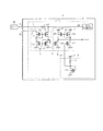
図1に示すように、IC1は、一般的なCMOSプロセスにより製造されており、例えば車載ECU(Electronic Control Unit)の制御基板に搭載されている。IC1は、車載センサからの信号電圧が入力される外部入力端子1a,電源電圧VDD(例えば5V)が供給される電源端子1bなど様々な端子を有している。外部入力端子1aは、入力信号線6を介してIC1に形成されている過電圧検出回路2に接続されている。過電圧検出回路2は、クランプ回路3,コンパレータ回路4及びバイアス回路5を備えている。クランプ回路3は電圧/電流変換部に相当し、コンパレータ回路4及びバイアス回路5は、コンパレータ部に相当する。
(First embodiment)
As shown in FIG. 1, the IC 1 is manufactured by a general CMOS process, and is mounted on, for example, a control board of an in-vehicle ECU (Electronic Control Unit). The IC 1 has various terminals such as an external input terminal 1a to which a signal voltage from an in-vehicle sensor is input and a power supply terminal 1b to which a power supply voltage VDD (for example, 5V) is supplied. The external input terminal 1 a is connected to the
入力信号線6の一端は外部入力端子1aに接続され、他端は検出用抵抗13を介してPチャネルMOSFET9のソースに接続されている。前記ソースは、内部入力端子に相当する。電源端子1bは電源線7を介してPチャネルMOSFET11のソースに接続されている。一例として、外部入力端子1aには、IC1の外部にあるセンサ素子28の出力端子が接続されている。また、FET9のソースは信号処理回路29の入力端子に接続されている。尚、IC1には、この他にも図示しない様々な回路が形成されている。
One end of the
クランプ回路3は、NチャネルMOSFET10及び12で構成される第1カレントミラー回路31と、FET9及び11で構成される第2カレントミラー回路32とを備えている。FET10及び12のソースはグランドに接続され、FET10のドレインはFET9のドレインに接続され、FET12のドレインはFET11のドレインに接続されている。ソース及びドレインは、導通端子に相当する。FET9及び11の導通制御端子であるゲートはFET11のドレインに接続され、FET10及び12のゲートはFET10のドレインに接続されている。
The
コンパレータ回路4は、PチャネルMOSFET18及び19で構成される第3カレントミラー回路33を備えており、FET18及び19のソースは、電源のシンボルで示す電源線7に接続されている。FET18及び19のゲートは、FET18のドレインに接続されている。また、FET18,19のドレインは、それぞれNチャネルMOSFET17,16のドレインに接続されている。FET17,16のソースはグランドに接続されている。FET16のゲートは、検出電圧入力線21を介してFET10のドレインに接続されており、両者はミラー対を構成している。FET17,16は、それぞれ第1,第2トランジスタに相当する。
The
バイアス回路5は、電源線7とグランドとの間に接続される、抵抗素子14及びNチャネルMOSFET15の直列回路で構成され、FET15のゲートは自身のドレインに接続されている。また、前記ドレインは、閾値電圧入力線20を介してFET17のゲートに接続されている。バイアス回路5は閾値設定部に相当する。そして、FET16のドレインが、コンパレータ回路4の出力端子Voutとなっている。出力端子Voutは、例えば上述したECUを構成するマイクロコンピュータ等の、図示しない制御回路の入力端子に接続されている。
The bias circuit 5 is composed of a series circuit of a
次に、本実施形態の作用について説明する。クランプ回路3では、FET11のソースに電源電圧VDDが与えられている。したがって、検出用抵抗13とFET9との共通接続点である内部入力端子の電圧は、(1)式のようにクランプ電圧Vclpに固定される。
Vclp=VDD−Vthp+Vthp …(1)
尚、VthpはFET9及び11の閾値電圧である。つまり、クランプ電圧Vclpは電源電圧VDDに設定されるので、クランプ電圧Vclpが過電圧検出回路2を構成する回路素子の耐圧を超えることはない。
Next, the operation of this embodiment will be described. In the
Vclp = VDD−Vthp + Vthp (1)
Vthp is the threshold voltage of the
図2に示すように、外部入力端子1aに印加される電圧Vinがクランプ電圧Vclpよりも低い場合、検出用抵抗13に電流IRは流れずFET9はオフとなる。したがって、クランプ回路3においては、リーク電流による信号入力線6の電圧変化を抑制できる。
As shown in FIG. 2, when the voltage Vin applied to the external input terminal 1a is lower than the clamp voltage Vclp, the current IR does not flow through the
電圧Vinがクランプ電圧Vclp以上になると、FET9〜12が何れもオンしてクランプ回路3が動作し、FET9のソース電圧はクランプ電圧Vclpに固定される。そして、外部入力端子1aより検出用抵抗13及びFET9を介して、電圧Vinとクランプ電圧Vclpとの差電圧ΔVに応じた検出電流Idet(=IR)が流れる。検出用抵抗13の抵抗値をRとすると、検出電流Idetは(2)式で示される。
Idet=ΔV/R=(Vin−Vclp)/R …(2)
また、FET10,12及び16はカレントミラー回路を構成しているので、検出用抵抗13に流れる検出電流Idetに応じた比較電流がFET16のドレイン電流IDとして流れる。例えばこれらのミラー比が「1」であれば、(比較電流)=(検出電流Idet)となる。これにより等価的に、クランプ電圧Vclp以上の電圧Vinを、回路素子耐圧以下の電圧に変換してコンパレータ回路4に入力できる。
When the voltage Vin becomes equal to or higher than the clamp voltage Vclp, the FETs 9 to 12 are all turned on to operate the
Idet = ΔV / R = (Vin−Vclp) / R (2)
Further, since the
バイアス回路5において、FET15のゲート及びドレインの電位は一定に制御されており、且つFET15及び17はミラー対を構成している。したがって、FET17には、FET15に流れるドレイン電流に応じたドレイン電流が、閾値電圧Vthに応じた閾値電流Ithとして流れる。尚、図2に示すI16,I17はそれぞれFET16,17のドレイン電流であり、V16,V17はそれぞれFET16,17のゲート電圧である。
In the bias circuit 5, the gate and drain potentials of the
コンパレータ回路4において(閾値電流Ith)>(比較電流Idet)であれば、出力端子Voutからは両者の差に応じた電流が出力される状態、つまりソース電流が流出する状態となり、FET16のドレイン電位が上昇して出力端子Voutの電圧はハイレベルを示す。一方、(閾値電流Ith)<(比較電流Idet)になると、出力端子Voutからは電流が出力されない状態、つまりシンク電流を引き込む状態となり、FET16のドレイン電位が低下して出力端子Voutの電圧はローレベルを示す。したがって、図2に示すように、比較電流Idetと閾値電流Ithとの大小関係に応じて、出力端子Voutの電圧レベルが変化する。
If (threshold current Ith)> (comparison current Idet) in the
以上のように本実施形態によれば、外部入力端子1aと内部入力端子との間に検出用抵抗13を接続する。クランプ回路3は、内部入力端子の電位を一定電圧にクランプし、外部入力端子1aに入力された電圧Vinがクランプ電圧Vclpを超えた際に、検出用抵抗13に流れる電流が通電される検出電流経路を有する。コンパレータ回路4の一方の電流経路には閾値電流Ithが通電され、他方の電流経路には、前記検出電流経路に流れる電流に応じた比較電流Idetが通電される。そして、比較電流の値が閾値電流の値を超えると、コンパレータ回路4は出力端子Voutの電圧レベルを変化させる。
As described above, according to the present embodiment, the
このように構成すれば、クランプ回路3の作用によりFET9のソース電位は一定の電源電圧VDDにクランプされるので、過電圧検出回路2を構成する回路素子の耐圧を超える電圧が印加されることを防止できる。また、クランプ回路3は、外部入力端子1aに印加される電圧を電流に変換して検出電流経路に流し、コンパレータ回路4は、前記経路に通電される電流に応じた比較電流Idetと閾値電流Ithとを比較して過電圧検出を行う。したがって、コンパレータ回路4における閾値電流Ithに対応する閾値電圧Vthを、電源電圧VDDよりも高い電圧に設定でき、過電圧検出回路2は、より広い電圧範囲について過電圧検出を行うことが可能になる。
With this configuration, the source potential of the FET 9 is clamped to the constant power supply voltage VDD by the action of the
具体的には、クランプ回路3を、グランド側に接続される第1カレントミラー回路31と、この第1カレントミラー回路31に直列に接続され、クランプ電圧Vclpを電源電圧VDDに設定する第2カレントミラー回路32とで構成する。そして、検出電流経路を第1カレントミラー回路31の基準電流経路とする。
Specifically, the
また、コンパレータ回路4を、電源側に接続される第3カレントミラー回路33と、当該回路33の基準電流経路,ミラー電流経路とグランドとの間にそれぞれ接続されるFET17,16とで構成し、コンパレータ部を、コンパレータ回路4と、前記基準電流経路に閾値電流が通電されるよう、FET17のゲートに制御信号を付与するバイアス回路5とで構成する。そして、FET16のゲートを第1カレントミラー回路31の基準電流経路に接続し、FET16のドレインをコンパレータ回路4の出力端子Voutとした。これにより、比較電流Idetと閾値電流Ithとの大小関係に応じて出力端子Voutの電圧レベルを変化させることができる。
Further, the
加えて、本実施形態の過電圧検出回路2は、例えば外部入力端子1aに接続されるセンサ素子28のように、センサ信号の検出精度が低下することを防止するため、検出回路側でリーク電流が極力発生しないことが望ましいものに好適である。
In addition, the
(第2実施形態)
以下、第1実施形態と同一部分には同一符号を付して説明を省略し、異なる部分について説明する。図3に示すように、第2実施形態のIC22に形成されている過電圧検出回路24は、クランプ電圧Vclpをグランド電位に設定するように構成されている。IC22の外部入力端子は22a,電源端子は22bとなっている。そして、IC22には、第1実施形態のクランプ回路3,コンパレータ回路4及びバイアス回路5に対応する、クランプ回路23,コンパレータ回路25及びバイアス回路34が形成されている。電源線7に対応するのは電源線26となっている。過電圧検出回路24は、入力電圧Vinが、グランド電位VGNDよりも低い負側の過電圧状態となったことを検出する。
(Second Embodiment)
Hereinafter, the same parts as those in the first embodiment are denoted by the same reference numerals, description thereof will be omitted, and different parts will be described. As shown in FIG. 3, the
クランプ回路23は、第1実施形態と同様のFET9〜12を備えているが、ソースが電源線26に接続されているFET9及び11によって、第2実施形態の第1カレントミラー回路35が構成されている。また、ソースがそれぞれグランドと検出用抵抗13の一端とに接続されているFET10及び12によって、第2カレントミラー回路36が構成されている。
The
コンパレータ回路25は、やはり第1実施形態と同様のFET16〜19を備えているが、ソースがグランドに接続されているFET16及び17によって、第3カレントミラー回路37が構成されている。FET16及び17のゲートは、FET17のドレインに接続されている。FET18,19は、第1実施形態と同様に電源線26とFET17,16との間に接続されており、これらはそれぞれ第1,第2トランジスタに相当する。FET19のゲートは、検出電圧入力線21を介してFET11のドレインに接続されており、両者はミラー対を構成している。
The
バイアス回路34は、電源線26とグランドとの間に接続される、PチャネルMOSFET38及び抵抗素子14の直列回路で構成されている。FET38のゲートは自身のドレインに接続されていると共に、閾値信号線20を介してFET18のゲートに接続されている。第1実施形態と同様に、FET16のドレインがコンパレータ回路25の出力端子Voutとなっている。
The
次に、第2実施形態の作用について説明する。クランプ回路23では、FET10のソースがグランドに接続されている。したがって、検出用抵抗13とFET12との共通接続点である内部入力端子の電圧は、(3)式のようにクランプ電圧Vclpに固定される。
Vclp=VGND+Vthn−Vthn …(3)
尚、VthnはFET10及び12の閾値電圧である。つまり、クランプ電圧Vclpはグランド電位VGNDに設定されるので、クランプ電圧Vclpが過電圧検出回路24を構成する回路素子の負側の耐圧を超えることはない。
Next, the operation of the second embodiment will be described. In the
Vclp = VGND + Vthn−Vthn (3)
Vthn is a threshold voltage of the
図4に示すように、外部入力端子22aに印加される電圧Vinがクランプ電圧Vclpよりも高い場合、検出用抵抗13に電流IRは流れずFET12はオフとなる。したがって、クランプ回路23において、リーク電流による信号入力線6の電圧変化を抑制できる。
As shown in FIG. 4, when the voltage Vin applied to the
電圧Vinがクランプ電圧Vclp以下になると、FET9〜12が何れもオンしてクランプ回路23が動作し、FET12のソース電圧はクランプ電圧Vclpに固定される。そして、FET12及び検出用抵抗13を介して、外部入力端子22aより電圧Vinとクランプ電圧Vclpとの差電圧ΔVに応じた検出電流Idetが流れる。検出電流Idetは、第1実施形態と同様に(2)式で示される。
When the voltage Vin becomes equal to or lower than the clamp voltage Vclp, the FETs 9 to 12 are all turned on to operate the
また、FET9,11及び19はカレントミラー回路を構成しているので、検出用抵抗13に流れる検出電流Idetに応じた比較電流がFET19に流れる。これにより等価的に、クランプ電圧Vclp以下の電圧Vinを、回路素子耐圧以内の電圧に変換してコンパレータ回路25に入力できる。
Further, since the
バイアス回路34において、FET38のゲート及びドレインの電位は一定に制御されており、且つFET38及び18はミラー対を構成している。したがって、FET18には、閾値電圧Vthに応じた閾値電流Ithがドレイン電流IDとして流れる。尚、図4に示すI18,I19はそれぞれFET18,19のドレイン電流であり、V18,V19はそれぞれFET18,19のゲート電圧である。
In the
コンパレータ回路25において、FET19のゲート電圧が高い状態にあり(閾値電流Ith)>(比較電流Idet)であれば、コンパ出力端子Voutからは電流が出力されない状態、つまりシンク電流を引き込む状態となり、FET16のドレイン電位が低下して出力端子Voutの電圧はローレベルを示す。
In the
FET19のゲート電圧が低下することでドレイン電流が増加し(閾値電流Ith)<(比較電流Idet)になると、出力端子Voutからは両者の差に応じた電流が出力される状態、つまりソース電流が流出する状態となり、FET16のドレイン電位が上昇して出力端子Voutの電圧はハイレベルを示す。したがって、図4に示すように、比較電流Idetと閾値電流Ithとの大小関係に応じて、出力端子Voutの電圧レベルが変化する。
When the gate voltage of the
以上のように第2実施形態によれば、クランプ回路23を、電源線26に接続される第1カレントミラー回路35と、当該回路35に直列に接続され、一定電圧をグランド電位VGNDに設定する第2カレントミラー回路36とで構成する。そして、検出電流経路を、第1カレントミラー回路35の基準電流経路とする。
As described above, according to the second embodiment, the
また、コンパレータ回路25を、グランド側に接続される第3カレントミラー回路37と、当該回路の基準電流経路,ミラー電流経路と電源との間に接続されるFET18,19とで構成し、コンパレータ部を、コンパレータ回路25と、前記基準電流経路に閾値電流Ithが通電されるよう、FET18のゲートに制御信号を付与するバイアス回路34とで構成する。そして、FET19のゲートを第1カレントミラー回路35の基準電流経路に接続し、第3カレントミラー回路37を構成するFET16のドレインをコンパレータ回路25の出力端子Voutとする。
The
したがって、コンパレータ回路25における閾値電流Ithに対応する閾値電圧Vthをグランド電位VGNDよりも低い電圧に設定でき、過電圧検出回路24は、負側のより広い電圧範囲について過電圧検出を行うことが可能になる。
Therefore, the threshold voltage Vth corresponding to the threshold current Ith in the
(その他の実施形態)
本発明は上記した、又は図面に記載した実施形態に限定されるものではなく、例えば以下のように変形または拡張が可能である。
コンパレータ回路4において、FET16及び17のソースを共通に接続し、電源線7との間に定電流源やNチャネルMOSFETを追加してもよい。
コンパレータ回路25において、FET18及び19のドレインを共通に接続し、電源線26との間に定電流源やPチャネルMOSFETを追加してもよい。
閾値電圧は、過電圧検出回路を構成する回路素子の耐圧以下に設定すれば良い。
各カレントミラー回路のミラー比については、個別の設計に応じて適宜設定すれば良い。
(Other embodiments)
The present invention is not limited to the embodiment described above or shown in the drawings, and can be modified or expanded as follows, for example.
In the
In the
The threshold voltage may be set to be equal to or lower than the withstand voltage of the circuit elements constituting the overvoltage detection circuit.
The mirror ratio of each current mirror circuit may be appropriately set according to the individual design.
MOSFETに替えて、バイポーラトランジスタを用いて過電圧検出回路を構成しても良い。
過電圧検出回路は、必ずしもICとして構成する必要はない。
外部入力端子に接続されるものはセンサ素子に限ることはない。実施形態の過電圧検出回路は特に、リーク電流の発生を極力抑制することが好ましいものを対象として過電圧検出を行う用途に好適である。
Instead of the MOSFET, an overvoltage detection circuit may be configured using a bipolar transistor.
The overvoltage detection circuit is not necessarily configured as an IC.
What is connected to the external input terminal is not limited to the sensor element. The overvoltage detection circuit of the embodiment is particularly suitable for applications in which overvoltage detection is performed for a circuit that preferably suppresses the generation of leakage current as much as possible.
1a 外部入力端子、1b 電源端子、2 過電圧検出回路、3 クランプ回路、4 コンパレータ回路、5 バイアス回路、13検出用抵抗、16及び17 NチャネルMOSFET、31 第1カレントミラー回路、32 第2カレントミラー回路、33 第3カレントミラー回路。 1a external input terminal, 1b power supply terminal, 2 overvoltage detection circuit, 3 clamp circuit, 4 comparator circuit, 5 bias circuit, 13 detection resistor, 16 and 17 N channel MOSFET, 31 first current mirror circuit, 32 second current mirror Circuit, 33 Third current mirror circuit.
Claims (5)
前記内部入力端子の電位を一定電圧にクランプすると共に、前記外部入力端子に入力された電圧が前記一定電圧を超えた際に、前記検出用抵抗に流れる電流が通電される検出電流経路を有する電圧/電流変換部(3,23)と、
一方の電流経路に予め定められた閾値電流が通電され、他方の電流経路には、前記検出電流経路に通電される電流に応じた比較電流が通電され、前記比較電流の値が前記閾値電流の値を超えると、出力電圧のレベルを変化させるコンパレータ部(4,25)とを備えることを特徴とする過電圧検出回路。 A detection resistor (13) connected between the external input terminal (1a, 22a) and the internal input terminal;
A voltage having a detection current path that clamps the potential of the internal input terminal to a constant voltage and through which a current flowing through the detection resistor is passed when the voltage input to the external input terminal exceeds the constant voltage. / Current converter (3, 23),
A predetermined threshold current is applied to one current path, a comparison current corresponding to the current applied to the detection current path is applied to the other current path, and the value of the comparison current is equal to the threshold current. An overvoltage detection circuit comprising a comparator section (4, 25) that changes the level of the output voltage when the value is exceeded.
前記内部入力端子及び電源端子(1b)と、前記第1カレントミラー回路との間に直列に接続され、前記一定電圧を、前記電源端子に入力される電源電圧に設定する第2カレントミラー回路(9,11)とで構成され、
前記検出電流経路は、前記内部入力端子を経路に含む前記第1カレントミラー回路の基準電流経路であり、
前記コンパレータ部(4)は、電源(7)側に接続される第3カレントミラー回路(18,19)と、
この第3カレントミラー回路の基準電流経路とグランドとの間に接続される第1トランジスタ(17)と、
前記第3カレントミラー回路のミラー電流経路とグランドとの間に接続される第2トランジスタ(16)と、
前記基準電流経路に前記閾値電流が通電されるように、前記第1トランジスタの導通制御端子に制御信号を付与する閾値設定部(5)とで構成され、
前記第2トランジスタの導通制御端子は、前記第1カレントミラー回路の基準電流経路に接続され、
前記第3カレントミラー回路を構成するトランジスタと前記第2トランジスタとの共通接続点が、出力端子となることを特徴とする請求項1記載の過電圧検出回路。 The voltage / current converter (3) includes a first current mirror circuit (10, 12) connected to the ground side,
A second current mirror circuit (connected in series between the internal input terminal and the power supply terminal (1b) and the first current mirror circuit, and setting the constant voltage to a power supply voltage input to the power supply terminal ( 9, 11),
The detection current path is a reference current path of the first current mirror circuit including the internal input terminal in the path;
The comparator unit (4) includes a third current mirror circuit (18, 19) connected to the power source (7) side,
A first transistor (17) connected between the reference current path of the third current mirror circuit and the ground;
A second transistor (16) connected between the mirror current path of the third current mirror circuit and the ground;
A threshold setting unit (5) for applying a control signal to the conduction control terminal of the first transistor so that the threshold current is passed through the reference current path;
The conduction control terminal of the second transistor is connected to a reference current path of the first current mirror circuit,
2. The overvoltage detection circuit according to claim 1, wherein a common connection point between the transistor constituting the third current mirror circuit and the second transistor serves as an output terminal.
前記第1カレントミラー回路と、前記内部入力端子及びグランドとの間に直列に接続され、前記一定電圧を、前記グランド電位に設定する第2カレントミラー回路(10,12)とで構成され、
前記検出電流経路は、前記内部入力端子を経路に含む前記第1カレントミラー回路の基準電流経路であり、
前記コンパレータ部(25)は、グランド側に接続される第3カレントミラー回路(16,17)と、
この第3カレントミラー回路の基準電流経路と電源との間に接続される第1トランジスタ(18)と、
前記第3カレントミラー回路のミラー電流経路とグランドとの間に接続される第2トランジスタ(19)と、
前記基準電流経路に前記閾値電流が通電されるように、前記第1トランジスタの導通制御端子に制御信号を付与する閾値設定部(5)とで構成され、
前記第2トランジスタの導通制御端子は、前記第1カレントミラー回路の基準電流経路に接続され、
前記第3カレントミラー回路を構成するトランジスタと、前記第2トランジスタとの共通接続点が出力端子となることを特徴とする請求項1記載の過電圧検出回路。 The voltage / current converter (23) includes a first current mirror circuit (9, 11) connected to the power supply terminal;
A first current mirror circuit, and a second current mirror circuit (10, 12) connected in series between the internal input terminal and the ground and setting the constant voltage to the ground potential;
The detection current path is a reference current path of the first current mirror circuit including the internal input terminal in the path;
The comparator unit (25) includes a third current mirror circuit (16, 17) connected to the ground side,
A first transistor (18) connected between a reference current path of the third current mirror circuit and a power source;
A second transistor (19) connected between the mirror current path of the third current mirror circuit and the ground;
A threshold setting unit (5) for applying a control signal to the conduction control terminal of the first transistor so that the threshold current is passed through the reference current path;
The conduction control terminal of the second transistor is connected to a reference current path of the first current mirror circuit,
2. The overvoltage detection circuit according to claim 1, wherein a common connection point between the transistor constituting the third current mirror circuit and the second transistor serves as an output terminal.
Priority Applications (1)
| Application Number | Priority Date | Filing Date | Title |
|---|---|---|---|
| JP2015120231A JP2017005609A (en) | 2015-06-15 | 2015-06-15 | Overvoltage detection circuit |
Applications Claiming Priority (1)
| Application Number | Priority Date | Filing Date | Title |
|---|---|---|---|
| JP2015120231A JP2017005609A (en) | 2015-06-15 | 2015-06-15 | Overvoltage detection circuit |
Publications (1)
| Publication Number | Publication Date |
|---|---|
| JP2017005609A true JP2017005609A (en) | 2017-01-05 |
Family
ID=57752379
Family Applications (1)
| Application Number | Title | Priority Date | Filing Date |
|---|---|---|---|
| JP2015120231A Pending JP2017005609A (en) | 2015-06-15 | 2015-06-15 | Overvoltage detection circuit |
Country Status (1)
| Country | Link |
|---|---|
| JP (1) | JP2017005609A (en) |
Cited By (2)
| Publication number | Priority date | Publication date | Assignee | Title |
|---|---|---|---|---|
| WO2023073802A1 (en) * | 2021-10-26 | 2023-05-04 | 三菱電機株式会社 | Semiconductor integrated circuit device |
| CN117434333A (en) * | 2023-12-01 | 2024-01-23 | 深圳智芯微电子科技有限公司 | Micro-grid line voltage abnormality detection circuit, energy management system and electric equipment |
Citations (2)
| Publication number | Priority date | Publication date | Assignee | Title |
|---|---|---|---|---|
| JPH04332876A (en) * | 1991-05-08 | 1992-11-19 | Fujitsu Ltd | Operation state detection circuit |
| JP2010011012A (en) * | 2008-06-26 | 2010-01-14 | Denso Corp | Comparator with clamping function |
-
2015
- 2015-06-15 JP JP2015120231A patent/JP2017005609A/en active Pending
Patent Citations (2)
| Publication number | Priority date | Publication date | Assignee | Title |
|---|---|---|---|---|
| JPH04332876A (en) * | 1991-05-08 | 1992-11-19 | Fujitsu Ltd | Operation state detection circuit |
| JP2010011012A (en) * | 2008-06-26 | 2010-01-14 | Denso Corp | Comparator with clamping function |
Cited By (2)
| Publication number | Priority date | Publication date | Assignee | Title |
|---|---|---|---|---|
| WO2023073802A1 (en) * | 2021-10-26 | 2023-05-04 | 三菱電機株式会社 | Semiconductor integrated circuit device |
| CN117434333A (en) * | 2023-12-01 | 2024-01-23 | 深圳智芯微电子科技有限公司 | Micro-grid line voltage abnormality detection circuit, energy management system and electric equipment |
Similar Documents
| Publication | Publication Date | Title |
|---|---|---|
| US8519782B2 (en) | Constant voltage circuit | |
| US9214910B2 (en) | Integrated circuit | |
| TW201107920A (en) | Voltage regulator | |
| US10050031B2 (en) | Power conventer and semiconductor device | |
| WO2007049597A1 (en) | Current detection circuit | |
| JP2021502049A5 (en) | ||
| US9419571B2 (en) | Precision, high voltage, low power differential input stage with static and dynamic gate protection | |
| JP2009044304A (en) | Semiconductor element controller | |
| KR20150095585A (en) | Dc/dc converter and electronic apparatus | |
| US20150033040A1 (en) | Power supply circuit for central processing unit | |
| JP2017005609A (en) | Overvoltage detection circuit | |
| JP2017135532A (en) | Voltage detection circuit and charge pump circuit | |
| US10551860B2 (en) | Regulator for reducing power consumption | |
| JP5272467B2 (en) | Semiconductor integrated circuit with built-in reference voltage generation circuit and reset circuit | |
| US20150198485A1 (en) | Temperature sensing circuits | |
| JP5465548B2 (en) | Level shift circuit | |
| JP6658269B2 (en) | Overcurrent detection circuit | |
| JP2010011012A (en) | Comparator with clamping function | |
| JP6202208B2 (en) | Power semiconductor device current detection device | |
| JP6672067B2 (en) | Stabilized power supply circuit | |
| JP3855810B2 (en) | Differential amplifier circuit | |
| JP4360267B2 (en) | Amplifier circuit | |
| JP2011205180A (en) | Current detection circuit | |
| JP2018061115A (en) | Enable signal generation circuit | |
| JP5428259B2 (en) | Reference voltage generation circuit and power supply clamp circuit |
Legal Events
| Date | Code | Title | Description |
|---|---|---|---|
| A621 | Written request for application examination |
Free format text: JAPANESE INTERMEDIATE CODE: A621 Effective date: 20170906 |
|
| A977 | Report on retrieval |
Free format text: JAPANESE INTERMEDIATE CODE: A971007 Effective date: 20180517 |
|
| A131 | Notification of reasons for refusal |
Free format text: JAPANESE INTERMEDIATE CODE: A131 Effective date: 20180612 |
|
| A02 | Decision of refusal |
Free format text: JAPANESE INTERMEDIATE CODE: A02 Effective date: 20181204 |