JP2016532974A - Integrated memory controller for heterogeneous memory on multichip packages - Google Patents
Integrated memory controller for heterogeneous memory on multichip packages Download PDFInfo
- Publication number
- JP2016532974A JP2016532974A JP2016538917A JP2016538917A JP2016532974A JP 2016532974 A JP2016532974 A JP 2016532974A JP 2016538917 A JP2016538917 A JP 2016538917A JP 2016538917 A JP2016538917 A JP 2016538917A JP 2016532974 A JP2016532974 A JP 2016532974A
- Authority
- JP
- Japan
- Prior art keywords
- memory
- interface
- host
- umc
- unit
- Prior art date
- Legal status (The legal status is an assumption and is not a legal conclusion. Google has not performed a legal analysis and makes no representation as to the accuracy of the status listed.)
- Ceased
Links
Images


Classifications
-
- G—PHYSICS
- G06—COMPUTING; CALCULATING OR COUNTING
- G06F—ELECTRIC DIGITAL DATA PROCESSING
- G06F13/00—Interconnection of, or transfer of information or other signals between, memories, input/output devices or central processing units
- G06F13/14—Handling requests for interconnection or transfer
- G06F13/16—Handling requests for interconnection or transfer for access to memory bus
- G06F13/1668—Details of memory controller
- G06F13/1694—Configuration of memory controller to different memory types
-
- G—PHYSICS
- G06—COMPUTING; CALCULATING OR COUNTING
- G06F—ELECTRIC DIGITAL DATA PROCESSING
- G06F3/00—Input arrangements for transferring data to be processed into a form capable of being handled by the computer; Output arrangements for transferring data from processing unit to output unit, e.g. interface arrangements
- G06F3/06—Digital input from, or digital output to, record carriers, e.g. RAID, emulated record carriers or networked record carriers
- G06F3/0601—Interfaces specially adapted for storage systems
- G06F3/0602—Interfaces specially adapted for storage systems specifically adapted to achieve a particular effect
- G06F3/0604—Improving or facilitating administration, e.g. storage management
-
- G—PHYSICS
- G06—COMPUTING; CALCULATING OR COUNTING
- G06F—ELECTRIC DIGITAL DATA PROCESSING
- G06F3/00—Input arrangements for transferring data to be processed into a form capable of being handled by the computer; Output arrangements for transferring data from processing unit to output unit, e.g. interface arrangements
- G06F3/06—Digital input from, or digital output to, record carriers, e.g. RAID, emulated record carriers or networked record carriers
- G06F3/0601—Interfaces specially adapted for storage systems
- G06F3/0628—Interfaces specially adapted for storage systems making use of a particular technique
- G06F3/0655—Vertical data movement, i.e. input-output transfer; data movement between one or more hosts and one or more storage devices
- G06F3/0658—Controller construction arrangements
-
- G—PHYSICS
- G06—COMPUTING; CALCULATING OR COUNTING
- G06F—ELECTRIC DIGITAL DATA PROCESSING
- G06F3/00—Input arrangements for transferring data to be processed into a form capable of being handled by the computer; Output arrangements for transferring data from processing unit to output unit, e.g. interface arrangements
- G06F3/06—Digital input from, or digital output to, record carriers, e.g. RAID, emulated record carriers or networked record carriers
- G06F3/0601—Interfaces specially adapted for storage systems
- G06F3/0668—Interfaces specially adapted for storage systems adopting a particular infrastructure
- G06F3/0671—In-line storage system
- G06F3/0683—Plurality of storage devices
Landscapes
- Engineering & Computer Science (AREA)
- Theoretical Computer Science (AREA)
- Physics & Mathematics (AREA)
- General Engineering & Computer Science (AREA)
- General Physics & Mathematics (AREA)
- Human Computer Interaction (AREA)
- Memory System (AREA)
Abstract
統合メモリコントローラを含む拡張型マルチチップパッケージ(eMCP)が提供される。UMCは、eMCP上のNANDフラッシュメモリやDRAMなどの異なるタイプのメモリを管理するように構成される。UMCは、記憶メモリ管理、DRAM管理、記憶メモリ管理のためのDRAMアクセス性、およびDRAM管理のための記憶メモリアクセス性を可能にする。UMCはまた、DRAMから記憶メモリへの、またはその逆の、データの直接コピーを容易にする。直接コピーは、ホストからの相互作用なしで、UMCによって開始することもでき、あるいは、ホストによって開始することもできる。An extended multi-chip package (eMCP) is provided that includes an integrated memory controller. UMC is configured to manage different types of memory such as NAND flash memory and DRAM on eMCP. UMC enables storage memory management, DRAM management, DRAM accessibility for storage memory management, and storage memory accessibility for DRAM management. UMC also facilitates direct copying of data from DRAM to storage memory or vice versa. A direct copy can be initiated by the UMC without interaction from the host, or it can be initiated by the host.
Description
本開示は一般に、集積記憶デバイスに関する。より詳細には、本開示は、集積記憶デバイス上の複数のメモリタイプの制御に関する。 The present disclosure relates generally to integrated storage devices. More particularly, this disclosure relates to the control of multiple memory types on an integrated storage device.
2タイプ以上のメモリを含む低コスト異種メモリ装置を、組込みマルチチップパッケージ(eMCP:embedded multi-chip package)上に構成することが可能である。異種メモリデバイス向けの現在のマルチチップパッケージ設計は、一般に、NANDフラッシュメモリ部分を含む記憶メモリ部分と、ダイナミックランダムアクセスメモリ(DRAM)部分とを、単一パッケージ上に含んでいる。状況に応じて、NANDフラッシュメモリまたはDRAMメモリのいずれかにアクセスすることが、これらの異なるメモリタイプが相対的な利益および不利点をもつため、より有利となり得る。DRAMは、データの各ビットを、集積回路内の別々のコンデンサに記憶する。この構造上の単純さにより、DRAMを非常に高密度で実装することが可能になっている。NANDフラッシュメモリは、不揮発性であり、低電力使用、小サイズ、および極めて高い性能を実現している。NANDフラッシュメモリとは異なり、DRAMは揮発性メモリであり、電力が遮断されるとそのデータをすぐに失う。 A low-cost heterogeneous memory device including two or more types of memories can be configured on an embedded multi-chip package (eMCP). Current multi-chip package designs for heterogeneous memory devices generally include a storage memory portion including a NAND flash memory portion and a dynamic random access memory (DRAM) portion on a single package. Depending on the situation, accessing either NAND flash memory or DRAM memory can be more advantageous because these different memory types have relative advantages and disadvantages. DRAM stores each bit of data on a separate capacitor in the integrated circuit. This structural simplicity allows DRAM to be mounted at very high density. NAND flash memory is non-volatile and provides low power usage, small size, and extremely high performance. Unlike NAND flash memory, DRAM is volatile memory and loses its data immediately when power is cut off.
異種メモリデバイス向けの現在のマルチチップパッケージ設計は、フラッシュメモリ用のホストインターフェース、およびDRAM用の別個のホストインターフェースを含んでいる。フラッシュメモリは、別個のコントローラに依存し、一般にそれ自体で使用することはできない。フラッシュメモリコントローラは一般に、フラッシュメモリホストインターフェースとフラッシュメモリとの間に結合される。フラッシュメモリとは異なり、現在のDRAMメモリは、個別のコントローラに依存せず、したがってDRAMは、マルチチップパッケージ上でDRAMホストインターフェースに直接接続することができる。 Current multi-chip package designs for heterogeneous memory devices include a host interface for flash memory and a separate host interface for DRAM. Flash memory relies on a separate controller and generally cannot be used on its own. A flash memory controller is generally coupled between the flash memory host interface and the flash memory. Unlike flash memory, current DRAM memory does not rely on a separate controller, so DRAM can be connected directly to the DRAM host interface on a multi-chip package.
フラッシュメモリとDRAMを両方備えたマルチチップパッケージは、DRAMとフラッシュメモリを別々に含むデバイスに代わる、より低コストの手段である。 Multi-chip packages with both flash memory and DRAM are a lower cost alternative to devices that contain DRAM and flash memory separately.
本開示の一態様による装置は、少なくとも1つの、第1のメモリタイプの第1のメモリと、少なくとも1つの、第1のメモリタイプとは異なる第2のメモリタイプの第2のメモリとを含む。装置は、第1のメモリおよび第2のメモリに結合された、統合メモリコントローラ(UMC:unified memory controller)も含む。UMCは、第1のメモリとホストとの間の第1のインターフェース、および第2のメモリとホストとの間の第2のインターフェースを含む。UMCは、第1のインターフェースとは独立した第2のメモリを制御および利用するように、第1のメモリにアクセスするように構成される。 An apparatus according to an aspect of the present disclosure includes at least one first memory of a first memory type and at least one second memory of a second memory type different from the first memory type. . The apparatus also includes a unified memory controller (UMC) coupled to the first memory and the second memory. The UMC includes a first interface between the first memory and the host, and a second interface between the second memory and the host. The UMC is configured to access the first memory to control and utilize a second memory that is independent of the first interface.
本開示の別の態様による装置は、少なくとも1つの、第1のメモリタイプの第1のメモリと、少なくとも1つの、第1のメモリタイプとは異なる第2のメモリタイプの第2のメモリとを含む。装置は、第1のメモリおよび第2のメモリに結合された、統合メモリコントローラ(UMC)も含む。UMCは、第1のメモリとホストとの間の第1のインターフェース、および第2のメモリとホストとの間の第2のインターフェースを含む。UMCは、第2のインターフェースを通じた第2のメモリへのホストアクセスを補助するように、第1のメモリを利用するように構成される。 An apparatus according to another aspect of the present disclosure includes at least one first memory of a first memory type and at least one second memory of a second memory type different from the first memory type. Including. The apparatus also includes an integrated memory controller (UMC) coupled to the first memory and the second memory. The UMC includes a first interface between the first memory and the host, and a second interface between the second memory and the host. The UMC is configured to utilize the first memory to assist host access to the second memory through the second interface.
本開示の別の態様によるメモリインターフェース方法は、マルチチップパッケージの第1のホストインターフェース上のホストから、(データやデータの要求などの)情報を受信することを含む。情報は、マルチチップパッケージ上の第1のメモリタイプの第1のメモリに記憶されたデータの要求とすることができる。情報は、マルチチップパッケージ上の第1のメモリに記憶させるべきデータとすることもできる。本方法は、第1のメモリにおけるデータの記憶、または第1のメモリにおけるデータの取出しを補助するように、マルチチップパッケージ上の第2のメモリタイプの第2のメモリに、マルチチップパッケージの第2のホストインターフェースとは独立にアクセスすることも含む。 A memory interface method according to another aspect of the present disclosure includes receiving information (such as data or a request for data) from a host on a first host interface of a multi-chip package. The information can be a request for data stored in a first memory of a first memory type on the multichip package. The information can also be data to be stored in the first memory on the multichip package. The method includes the second memory type second memory on the multi-chip package in a second memory type second memory on the multi-chip package to assist in storing data in the first memory or retrieving data in the first memory. Including access independently from the host interface of the second.
本開示の別の態様によるメモリインターフェース装置は、マルチチップパッケージの第1のホストインターフェース上のホストから、マルチチップパッケージ上の第1のメモリタイプの第1のメモリに記憶させるべきデータを受信するための手段を含む。本装置は、第1のメモリにおけるデータの記憶を補助するように、マルチチップパッケージ上の第2のメモリタイプの第2のメモリに、マルチチップパッケージの第2のホストインターフェースとは独立にアクセスするための手段も含む。 A memory interface device according to another aspect of the present disclosure receives data to be stored in a first memory of a first memory type on a multi-chip package from a host on a first host interface of the multi-chip package. Including means. The device accesses the second memory of the second memory type on the multichip package independently of the second host interface of the multichip package to assist in storing data in the first memory. Means for including.
上記では、続く詳細な説明をよりよく理解することができるように、本開示の特徴および技術的利点について、かなり大まかに概説してきた。本開示のさらなる特徴および利点について、以下に説明する。本開示は、本開示と同じ目的を果たすための他の構造(structure)を修正または設計する基礎として容易に利用できることを、当業者には理解されたい。そのような等価な構造(construction)が、添付の特許請求の範囲に記載の本開示の教示から逸脱しないことも、当業者には理解されたい。本開示の構成(organization)と動作方法の両方に関して本開示の特徴になると考えられる新規な特徴と、さらなる目的および利点がともに、以下の説明を添付の図と併せ検討することからよりよく理解されるであろう。しかしながら、図の各々は、例示および説明を目的として提供されているに過ぎず、本開示の制限を定めるものではないことを、明確に理解されたい。 The foregoing has outlined rather broadly the features and technical advantages of the present disclosure in order that the detailed description that follows may be better understood. Additional features and advantages of the present disclosure are described below. Those skilled in the art will appreciate that the present disclosure can be readily utilized as a basis for modifying or designing other structures to serve the same purpose as the present disclosure. It should also be understood by those skilled in the art that such equivalent constructions do not depart from the teachings of the present disclosure as set forth in the appended claims. Both the novel features that are believed to be features of this disclosure, as well as further objects and advantages, both in terms of the organization and method of operation of this disclosure, are better understood from a review of the following description in conjunction with the accompanying figures. It will be. However, it should be clearly understood that each of the figures is provided for purposes of illustration and description only and does not define limitations of the present disclosure.
本開示のより完全な理解が得られるように、ここで、以下の説明を添付の図面と併せて参照されたい。 For a fuller understanding of the present disclosure, reference is now made to the following description, taken in conjunction with the accompanying drawings, in which:
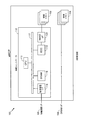
図1は、異種メモリを含む組込みマルチチップパッケージ(eMCP)100を示す。異種メモリは、第1のメモリタイプの第1のメモリ102、および第1のメモリタイプとは異なる第2のメモリタイプの第2のメモリ104を含む。図示のeMCP100では、第1のメモリ102が、NAND記憶メモリであり、第2のメモリ104が、ダイナミックランダムアクセスメモリ(DRAM)である。eMCP100は、第1のホストインターフェース106、および第2のホストインターフェース108を含む。eMCP100上のメモリコントローラ110が、第1のホストインターフェース106と第1のメモリ102との間に結合される。第2のホストインターフェース108は、第2のメモリ104に直接結合される。第2のメモリ104は、コントローラ回路に依存せず、メモリコントローラ110が管理することができない。
FIG. 1 illustrates an embedded multi-chip package (eMCP) 100 that includes heterogeneous memory. The heterogeneous memory includes a
メモリコントローラ110は、中央処理装置112と、メモリコントローラバス117を通じてそれに結合された、ホストインターフェース回路114と、スタティックランダムアクセスメモリ(SRAM)116と、誤り訂正コード回路(ECC)118と、記憶メモリインターフェース回路120とを含む。ホストインターフェース回路114は、第1のホストインターフェース106に結合され、記憶メモリインターフェース回路120は、第1のメモリ102に結合される。
The
図1に示すeMCP100などの現在のeMCPは、NANDフラッシュメモリなどの記憶メモリ、およびDRAMメモリなどの第2のメモリを、単一パッケージ内に集積している。しかしながら、現在のeMCP設計では、2つの異なるメモリは一般に互いに相互作用しない。 Current eMCPs, such as eMCP 100 shown in FIG. 1, integrate storage memory, such as NAND flash memory, and second memory, such as DRAM memory, in a single package. However, in current eMCP designs, two different memories generally do not interact with each other.
eMCP100では、メモリコントローラ110が、NAND記憶メモリ102をサポートするためのいくつかの機能を実行する。メモリコントローラ110の重要な機能の1つが、ホストインターフェース上で受信した論理アドレスを、たとえば、NAND記憶メモリ102内の対応する物理アドレスに変換することである。この変換用のマッピングテーブルは一般に、非常に大きく、大量の記憶容量を消費する。eMCP100では、SRAM116が、大きなマッピングテーブルを記憶する。しかしながら、NAND記憶メモリのサイズが増加するにつれて、マッピングテーブルを記憶させるためにSRAMを使用することが、ますます高価になる。たとえば、満足の行く性能を維持するために、32ギガバイト(GB)のNAND記憶メモリであれば、マッピングテーブルを記憶させるために、約32メガバイト(MB)のSRAMまたは他の何らかの揮発性メモリを使用することになる。
In eMCP 100,
NAND記憶メモリ102とは異なり、現在のeMCP100内の第2のメモリ104などのDRAMは一般に、コントローラ回路による管理に依存しない。図1に示すeMCP100などの現在のeMCPでは、DRAMメモリを管理することはできない。しかしながら、DRAM回路の制御が将来的に有益となり得ることが、大いに予想される。たとえば、プロセスの改良により、DRAMセルのサイズがさらに縮小するにつれて、将来的なDRAMセルの品質が悪化することが予期される。したがって、DRAMは、許容可能な性能を維持するために、最終的にはコントローラ回路による何らかの管理に依存することになると予想される。
Unlike the
本開示の態様は、eMCP上のNANDフラッシュメモリやDRAMなどの異なるタイプのメモリを管理するように構成された統合メモリコントローラ(UMC)を含む、eMCPを提供する。統合メモリコントローラは、記憶メモリ管理、DRAM管理、記憶メモリ管理のためのDRAMアクセス性、およびDRAM管理のための記憶メモリアクセス性を可能にする。統合メモリコントローラはまた、DRAMから記憶メモリへの、またはその逆の、データの直接コピーを容易にする。直接コピーは、ホストからの相互作用なしで、統合メモリコントローラによって開始することもでき、あるいは、たとえば特別なコマンドまたはモードを使用して、ホストによって開始することもできる。本開示の態様によれば、eMCPは、記憶メモリおよびDRAMメモリ用に、別々のホストインターフェースを含む。 Aspects of the present disclosure provide an eMCP that includes an integrated memory controller (UMC) configured to manage different types of memory, such as NAND flash memory and DRAM on the eMCP. The integrated memory controller enables storage memory management, DRAM management, DRAM accessibility for storage memory management, and storage memory accessibility for DRAM management. The integrated memory controller also facilitates direct copying of data from DRAM to storage memory or vice versa. A direct copy can be initiated by the integrated memory controller without interaction from the host, or it can be initiated by the host, for example using a special command or mode. According to aspects of the present disclosure, the eMCP includes separate host interfaces for storage memory and DRAM memory.
図2Aは、本開示の態様に従って異なるメモリタイプの制御を容易にする、異種メモリを含むeMCP200を示す。図2Aに示す図は、平面内に構成されたeMCP200の各構成要素を示しているが、構成要素は、たとえば、ワイヤボンディングおよび/またはシリコン貫通ビア(TSV)を用いて積層することによって、配置することもできることを理解されたい。異種メモリは、第1のメモリタイプの第1のメモリ202、および第1のメモリタイプとは異なる第2のメモリタイプの第2のメモリ204を含む。図示のeMCP200では、第1のメモリ202が、NAND記憶メモリであり、第2のメモリ204が、ダイナミックランダムアクセスメモリ(DRAM)である。eMCP200は、第1のホストインターフェース206、および第2のホストインターフェース208を含む。eMCP200上の統合メモリコントローラ(UMC)210が、第1のホストインターフェース206と第1のメモリ202との間、および第2のホストインターフェース208と第2のメモリ204との間に結合される。
FIG. 2A illustrates an
統合メモリコントローラ210は、中央処理装置(CPU)212と、統合メモリコントローラバス217を通じてそれに結合された、第1のホストインターフェース回路214と、スタティックランダムアクセスメモリ(SRAM)216と、誤り訂正コード回路(ECC)218とを含む。ECC回路218に、第1のメモリインターフェース回路220が結合される。第1のホストインターフェース206が、第1のホストインターフェース回路214に結合され、第1のメモリ202が、第1のメモリインターフェース回路220に結合される。統合メモリコントローラ210は、第2のホストインターフェース208に結合された第2のホストインターフェース回路222と、それに(アービタ回路230を通じて)結合された第2のメモリインターフェース回路224も含み、第2のメモリインターフェース回路224は、第2のメモリ204に結合される。第2のホストインターフェース回路222は、コマンドデータバッファ226を含み、統合メモリコントローラ210内のアービタ回路230に結合される。
The
本開示の一態様によれば、統合メモリコントローラ210は、バス217およびアービタ230に結合されたDRAMマネージャ228も含む。統合メモリコントローラ210は、NANDコントローラの機能を拡大して、統合メモリコントローラ210によるDRAM(たとえば第2のメモリ204)へのアクセスも行う。
According to one aspect of the present disclosure, the
本開示の態様によるeMCP200の1つの利点は、2つの異なるタイプのメモリを管理するために1つのコントローラを共用することのできる能力である。図2Bを参照すると、本開示の態様による統合メモリコントローラ210は、たとえば、経路238に沿って第2のメモリ204の直接制御を可能にする、DRAMマネージャ228を含む。単一の統合メモリコントローラ210を使用することにより、CPU212、SRAM216、ビルトインセルフテスト(BIST)回路(図示せず)などのような、コントローラの様々なリソースを共用することが可能になる。これにより、2つの異なるメモリタイプの各々について、別々のコントローラを実装するコストと比較して、コントローラの全体的なコストおよびサイズが減少する。
One advantage of
本開示の態様によるeMCP200は、たとえば統合メモリコントローラバス217およびCPU212を経由する、第1のホストインターフェース206と第1のメモリ202との間の経路232に沿った第1のメモリ202へのホストアクセスを、従来通りに可能にする。eMCP200は、たとえば統合メモリコントローラバス217またはCPU212との相互作用を伴わない、経路234に沿った第2のメモリ204へのホストアクセスも、従来通りに可能にする。
An
本開示の態様によるeMCP200の別の利点は、統合メモリコントローラ210が、第1のメモリ202の管理の実行を助けるために、第2のメモリ204に(たとえば経路236に沿って)アクセスすることができることである。たとえば、第1のメモリ202の制御機能を実行するのに使用されるSRAM216は一般に、DRAMよりもずっと小さく、DRAMより高価なので、統合メモリコントローラ210がDRAMにアクセスすることにより、第1のメモリ202のより効率的な制御が可能になる。DRAMへのコントローラアクセスを実現することにより、コントローラの一部としてのSRAMを増やすのと比較して、コストが節減される。
Another advantage of the
同様に、本開示の態様は、eMCP200上の不揮発性メモリタイプを、eMCP200上の揮発性メモリタイプを管理するための情報を記憶させるのに使用できるようにする。たとえば、NANDメモリは不揮発性であり、DRAMメモリは揮発性なので、DRAM(第2のメモリ204)を管理するための情報を、NANDメモリ(第1のメモリ202)に、たとえば経路236を通じて記憶させることができる。次いで、NANDメモリからのデータを使用して、DRAMをより効率的に管理することができる。
Similarly, aspects of the present disclosure allow non-volatile memory types on
eMCP200は、たとえば、DRAM(第2のメモリ204)の2つのアクセスが同時に開始されたときにアービトレーション機能を実行することのできる、アービタ230を含むことができる。eMCP200は、たとえば別のDRAMアクセスが完了するまでの間アービタ230が遅延させるDRAMアクセスに関連する、待ち状態のコマンドおよび/またはデータを記憶することのできる、コマンドデータバッファ226も含むことができる。
The
本開示の態様については、図2に示す第1のホストインターフェース206や第2のホストインターフェース208など、2つ以上のホストインターフェースを含むeMCP設計に即して説明しているが、他のeMCP設計は、単一のホストインターフェースを含むことができることを理解されたい。たとえば、図2Aに示すeMCP200は、本開示の一態様に従って、単一のホストインターフェースを有することができる。単一のホストインターフェースは、たとえば、第1のホストインターフェース206と同じタイプでもよく、第2のホストインターフェース208と同じタイプでもよい。
While aspects of the present disclosure are described in the context of an eMCP design that includes two or more host interfaces, such as the
本開示の態様については、異種メモリタイプがNANDフラッシュメモリおよびDRAMを含む、eMCP設計に即して説明しているが、他のメモリタイプをeMCP上に、本開示の態様による統合メモリコントローラとともに実装できることを理解されたい。たとえば、本開示の態様による統合メモリコントローラとともに実装することのできる、他の異種メモリタイプとして、磁気ランダムアクセスメモリ(MRAM)とDRAM、MRAMとNANDメモリ、またはPCRAMとNANDメモリなどがある。 Aspects of the present disclosure are described in the context of an eMCP design, where heterogeneous memory types include NAND flash memory and DRAM, but other memory types are implemented on the eMCP with an integrated memory controller according to aspects of the present disclosure. Please understand that you can. For example, other heterogeneous memory types that can be implemented with an integrated memory controller according to aspects of the present disclosure include magnetic random access memory (MRAM) and DRAM, MRAM and NAND memory, or PCRAM and NAND memory.
図3は、本開示の一態様によるメモリインターフェース方法300を示す、プロセスフロー図である。ブロック302において、メモリインターフェース方法300は、組込みマルチチップパッケージの第1のホストインターフェース上のホストから、情報を受信するステップを含む。情報は、マルチチップパッケージ上の第1のメモリタイプの第1のメモリに記憶させるべきデータとすることができる。情報は、マルチチップパッケージ上の第1のメモリに記憶されたデータの要求とすることもできる。ブロック304において、メモリインターフェース方法300は、マルチチップパッケージ上の第2のメモリタイプの第2のメモリにアクセスするステップを含む。アクセスするステップは、マルチチップパッケージの第2のホストインターフェースとは独立に行われる。アクセスするステップは、第1のメモリにデータを記憶させるように、または第1のメモリからデータを取り出すようにすることができる。
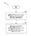
FIG. 3 is a process flow diagram illustrating a
本開示の一態様によるメモリインターフェース装置は、マルチチップパッケージの第1のホストインターフェース上のホストからデータを受信するための手段と、マルチチップパッケージ上の第2のメモリタイプの第2のメモリにアクセスするための手段とを含む。ホストからデータを受信するための手段は、たとえば、図2に示すeMCP200の第1のホストインターフェース206に結合された第1のホストインターフェース回路214を含むことができる。第2のメモリに、第2のホストインターフェースとは独立にアクセスするための手段は、たとえば、図2に示す統合メモリコントローラバス217に結合されたDRAMマネージャ228を含むことができる。
A memory interface device according to one aspect of the present disclosure includes means for receiving data from a host on a first host interface of a multichip package and accessing a second memory of a second memory type on the multichip package Means. The means for receiving data from the host can include, for example, a first
別の構成では、前述の手段は、前述の手段によって挙げられる機能を実行するように構成された任意のモジュールまたは任意の装置とすることができる。特定の手段について記載してきたが、開示した手段がすべて、開示した構成を実施するのに必要になるとは限らないことを、当業者なら理解されよう。その上、ある特定のよく知られた手段については、本開示に常に焦点を置くために説明していない。 In another configuration, the aforementioned means may be any module or any device configured to perform the functions listed by the aforementioned means. While specific means have been described, those skilled in the art will appreciate that not all disclosed means are required to implement the disclosed arrangement. Moreover, certain well-known means have not been described in order to always focus on the present disclosure.
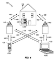
図4は、本開示の一態様が有利に採用され得る例示的なワイヤレス通信システム400を示すブロック図である。説明のために、図4は、3つの遠隔ユニット420、430、および450、ならびに2つの基地局440を示す。ワイヤレス通信システムは、より多くの遠隔ユニットおよび基地局を有することができることが、理解されよう。遠隔ユニット420、430、および450は、開示したeMCPを含んだICデバイス425A、425C、および425Bを含む。基地局、スイッチングデバイス、ネットワーク機器などの他のデバイスも、開示したeMCPを含むことができることが理解されよう。図4は、基地局440から遠隔ユニット420、430、および450への順方向リンク信号480、ならびに遠隔ユニット420、430、および450から基地局440への逆方向リンク信号490を示す。
FIG. 4 is a block diagram illustrating an example
図4では、遠隔ユニット420は、モバイル電話として示されており、遠隔ユニット430は、ポータブルコンピュータとして示されており、遠隔ユニット450は、ワイヤレスローカルループシステム内の固定位置遠隔ユニットとして示されている。たとえば、遠隔ユニットは、モバイル電話、ハンドヘルドパーソナル通信システム(PCS)ユニット、携帯情報端末などのポータブルデータユニット、GPS対応デバイス、ナビゲーションデバイス、セットトップボックス、音楽プレーヤ、ビデオプレーヤ、エンターテインメントユニット、検針機器などの固定位置データユニット、またはデータもしくはコンピュータ命令を記憶する、もしくは取り出す他のデバイス、またはそれらの組合せとすることができる。図4は、本開示の教示による遠隔ユニットを示しているが、本開示は、図示したこれらの例示的なユニットに限定されない。本開示の態様は、開示したeMCPを含む多くのデバイスにおいて、適切に採用され得る。
In FIG. 4,
図5は、上記で開示したeMCPなどの半導体構成要素の回路設計、レイアウト設計、および論理設計に使用される、設計用ワークステーションを示すブロック図である。設計用ワークステーション500は、オペレーティングシステムソフトウェア、サポートファイル、およびCadenceやOrCADなどの設計ソフトウェアを収容する、ハードディスク501を含む。設計用ワークステーション500は、回路デザイン510またはeMCPなどの半導体構成要素512の設計を容易にするためのディスプレイ502も含む。回路デザイン510または半導体構成要素512を有形に記憶させるために、記憶媒体504が用意される。回路デザイン510または半導体構成要素512は、記憶媒体504上に、GDSIIやGERBERなどのファイル形式で記憶させることができる。記憶媒体504は、CD-ROM、DVD、ハードディスク、フラッシュメモリ、または他の適切なデバイスとすることができる。さらに、設計用ワークステーション500は、記憶媒体504から入力を受け取る、または記憶媒体504に出力を書き込むための、ドライブ装置503を含む。
FIG. 5 is a block diagram illustrating a design workstation used for circuit design, layout design, and logic design of semiconductor components such as eMCP disclosed above. The
記憶媒体504上に記録されるデータは、論理回路構成、フォトリソグラフィマスク用のパターンデータ、または電子ビームリソグラフィなどのシリアル書き込みツール用のマスクパターンデータを詳述することができる。データはさらに、論理シミュレーションに関連するタイミングダイアグラムやネット回路などの論理検証データも含むことができる。記憶媒体504上にデータを提供すると、半導体ウェハーを設計するためのプロセス数が減少することによって、回路デザイン510または半導体構成要素512の設計が容易になる。
Data recorded on the
ファームウェアおよび/またはソフトウェアによる実装の場合、本明細書において説明した機能を実行するモジュール(たとえば手続き、関数など)を用いて、方法を実装することができる。本明細書において説明した方法を実装する際に、命令を有形に具現化するマシン可読媒体を使用することができる。たとえば、ソフトウェアコードをメモリに記憶させ、プロセッサユニットによって実行することができる。メモリは、プロセッサユニット内またはプロセッサユニットの外部に実装されていてよい。本明細書では、「メモリ」という用語は、長期メモリ、短期メモリ、揮発性メモリ、不揮発性メモリ、または他のメモリのタイプを指し、特定のタイプのメモリもしくは特定の数のメモリ、またはメモリが格納される媒体のタイプに限定すべきではない。 For firmware and / or software implementations, the methods can be implemented using modules (eg, procedures, functions, etc.) that perform the functions described herein. In implementing the methods described herein, a machine-readable medium that tangibly embodies instructions can be used. For example, software code can be stored in memory and executed by a processor unit. The memory may be implemented within the processor unit or external to the processor unit. As used herein, the term “memory” refers to a type of long-term memory, short-term memory, volatile memory, non-volatile memory, or other memory, where a particular type of memory or a particular number of memories, or memories It should not be limited to the type of media being stored.
機能は、ファームウェアおよび/またはソフトウェアとして実装される場合、1つまたは複数の命令またはコードとして、コンピュータ可読媒体上に記憶させることができる。例として、データ構造を符号化したコンピュータ可読媒体、およびコンピュータプログラムを符号化したコンピュータ可読媒体がある。コンピュータ可読媒体は、物理的なコンピュータ記憶媒体を含む。記憶媒体は、コンピュータがアクセスすることのできる利用可能な媒体とすることができる。限定ではなく例として、そのようなコンピュータ可読媒体には、RAM、ROM、EEPROM、CD-ROMもしくは他の光学ディスク記憶装置、磁気ディスク記憶装置もしくは他の磁気記憶デバイス、または命令もしくはデータ構造の形をとる所望のプログラムコードを記憶させるのに使用することができ、またコンピュータがアクセスすることのできる、他の媒体があり得る。ディスク(disk)およびディスク(disc)は、本明細書では、コンパクトディスク(CD:compact disc)、レーザディスク(laser disc)、光ディスク(optical disc)、デジタル多用途ディスク(DVD:digital versatile disc)、フロッピー(登録商標)ディスク(floppy disk)、およびブルーレイディスク(blu-ray disc)を含み、ただし、ディスク(disk)は通常、データを磁気的に再生し、一方ディスク(disc)は、レーザを用いてデータを光学的に再生する。上記の組合せも、コンピュータ可読媒体の範囲内に含まれるべきである。 The functionality, if implemented as firmware and / or software, can be stored on a computer-readable medium as one or more instructions or code. Examples include computer readable media encoded data structures and computer readable media encoded computer programs. Computer-readable media includes physical computer storage media. A storage media may be any available media that can be accessed by a computer. By way of example, and not limitation, such computer-readable media includes RAM, ROM, EEPROM, CD-ROM or other optical disk storage, magnetic disk storage or other magnetic storage device, or in the form of instructions or data structures. There may be other media that can be used to store the desired program code that can be stored on the computer and that can be accessed by the computer. In this specification, a disk and a disc are a compact disc (CD: compact disc), a laser disc (laser disc), an optical disc (optical disc), a digital versatile disc (DVD), Includes floppy disks and blu-ray discs, where the disk normally reproduces data magnetically, while the disc uses a laser. To optically reproduce the data. Combinations of the above should also be included within the scope of computer-readable media.
コンピュータ可読媒体における記憶に加えて、命令および/またはデータは、通信装置に含まれる伝送媒体における信号としても提供され得る。たとえば、通信装置は、命令およびデータを表す信号を有するトランシーバを含むことができる。命令およびデータは、1つまたは複数のプロセッサに、特許請求の範囲において概説する機能を実施させるように構成される。 In addition to storage on computer readable media, instructions and / or data may also be provided as signals on transmission media included in the communication devices. For example, the communication device can include a transceiver having signals representing instructions and data. The instructions and data are configured to cause one or more processors to perform the functions outlined in the claims.
以上、本開示およびその利点について詳細に説明してきたが、添付の特許請求の範囲によって定められる本開示の技術から逸脱することなく、本明細書において様々な変更、置換、および改変を行えることを理解されたい。たとえば、メモリのタイプとしてSRAMおよびMRAMについて説明したが、DRAM、PCRAMなどのような他のメモリタイプも企図される。その上、本願の範囲が、本明細書において説明したプロセス、マシン、製造、組成物、手段、方法、およびステップの特定の構成に限定されることは意図していない。当業者なら本開示から容易に理解するように、本明細書において説明した対応する構成と実質的に同じ機能を実行する、またはそれと実質的に同じ結果を達成する、現存するまたは後に開発されるプロセス、マシン、製造、組成物、手段、方法、またはステップを、本開示に従って利用することができる。したがって、添付の特許請求の範囲が、そのようなプロセス、マシン、製造、組成物、手段、方法、またはステップをその範囲内に含むことが意図される。 Although the present disclosure and its advantages have been described in detail above, various changes, substitutions, and modifications can be made herein without departing from the technology of the present disclosure as defined by the appended claims. I want you to understand. For example, although SRAM and MRAM have been described as memory types, other memory types such as DRAM, PCRAM, etc. are contemplated. Moreover, it is not intended that the scope of the application be limited to the specific configurations of the processes, machines, manufacture, compositions, means, methods, and steps described herein. Those of ordinary skill in the art will readily appreciate from the present disclosure to perform substantially the same function as the corresponding configuration described herein, or to achieve substantially the same result, existing or later developed Any process, machine, manufacture, composition, means, method, or step may be utilized in accordance with the present disclosure. Accordingly, the appended claims are intended to include within their scope such processes, machines, manufacture, compositions of matter, means, methods, or steps.
200 eMCP
202 第1のメモリ
204 第2のメモリ
206 第1のホストインターフェース
208 第2のホストインターフェース
210 統合メモリコントローラ(UMC)
212 中央処理装置(CPU)
214 第1のホストインターフェース回路
216 スタティックランダムアクセスメモリ(SRAM)
217 統合メモリコントローラバス
218 誤り訂正コード回路(ECC)、ECC回路
220 第1のメモリインターフェース回路
222 第2のホストインターフェース回路
224 第2のメモリインターフェース回路
226 コマンドデータバッファ
228 DRAMマネージャ
230 アービタ回路
300 メモリインターフェース方法
400 ワイヤレス通信システム
420 遠隔ユニット
425A ICデバイス
425B ICデバイス
425C ICデバイス
430 遠隔ユニット
440 基地局
450 遠隔ユニット
480 順方向リンク信号
490 逆方向リンク信号
500 設計用ワークステーション
501 ハードディスク
502 ディスプレイ
503 ドライブ装置
504 記憶媒体
510 回路デザイン
512 半導体構成要素
200 eMCP
202 First memory
204 Second memory
206 First host interface
208 Second host interface
210 Unified Memory Controller (UMC)
212 Central processing unit (CPU)
214 First host interface circuit
216 Static random access memory (SRAM)
217 Integrated memory controller bus
218 Error correction code circuit (ECC), ECC circuit
220 First memory interface circuit
222 Second host interface circuit
224 Second memory interface circuit
226 Command data buffer
228 DRAM Manager
230 Arbiter circuit
300 Memory interface method
400 wireless communication system
420 Remote unit
425A IC device
425B IC device
425C IC device
430 remote unit
440 base station
450 Remote unit
480 Forward link signal
490 Reverse link signal
500 design workstation
501 hard disk
502 display
503 drive unit
504 storage media
510 Circuit design
512 Semiconductor components
Claims (21)
少なくとも1つの、前記第1のメモリタイプとは異なる第2のメモリタイプの第2のメモリと、
前記第1のメモリおよび前記第2のメモリに結合された、統合メモリコントローラ(UMC)であって、前記第1のメモリとホストとの間の第1のインターフェース、および前記第2のメモリと前記ホストとの間の第2のインターフェースを含み、前記第1のインターフェースとは独立した前記第2のメモリを制御および利用するように、前記第1のメモリにアクセスするように構成される、UMCと
を備える装置。 At least one first memory of the first memory type; and
At least one second memory of a second memory type different from the first memory type;
A unified memory controller (UMC) coupled to the first memory and the second memory, the first interface between the first memory and a host; and the second memory and the A UMC comprising a second interface with a host and configured to access the first memory to control and utilize the second memory independent of the first interface; A device comprising:
をさらに備える、請求項1に記載の装置。 A multi-chip package (MCP), wherein the first memory is configured on a first chip of the MCP, and the second memory is configured on a second chip of the MCP.
The apparatus of claim 1, further comprising:
少なくとも1つの、前記第1のメモリタイプとは異なる第2のメモリタイプの第2のメモリと、
前記第1のメモリおよび前記第2のメモリに結合された、統合メモリコントローラ(UMC)であって、前記第1のメモリとホストとの間の第1のインターフェース、および前記第2のメモリと前記ホストとの間の第2のインターフェースを含み、前記第2のインターフェースを通じた前記第2のメモリへのホストアクセスを補助するように、前記第1のメモリを利用するように構成される、UMCと
を備える装置。 At least one first memory of the first memory type; and
At least one second memory of a second memory type different from the first memory type;
A unified memory controller (UMC) coupled to the first memory and the second memory, the first interface between the first memory and a host; and the second memory and the A UMC comprising a second interface with a host and configured to utilize the first memory to assist host access to the second memory through the second interface; A device comprising:
前記第1のメモリにおける前記動作を補助するように、前記マルチチップパッケージ上の第2のメモリタイプの第2のメモリに、前記マルチチップパッケージの第2のホストインターフェースとは独立にアクセスするステップと
を含む、メモリインターフェース方法。 Receiving information about operation in a first memory of a first memory type on the multichip package from a host on a first host interface of the multichip package;
Accessing a second memory type second memory on the multi-chip package independently of a second host interface of the multi-chip package to assist the operation in the first memory; A memory interface method.
前記第1のメモリにおける前記データの記憶を補助するように、前記マルチチップパッケージ上の第2のメモリタイプの第2のメモリに、前記マルチチップパッケージの第2のホストインターフェースとは独立にアクセスするための手段と
を備える、メモリインターフェース装置。 Means for receiving data to be stored in a first memory of a first memory type on the multichip package from a host on a first host interface of the multichip package;
Accessing the second memory of the second memory type on the multi-chip package independently from the second host interface of the multi-chip package to assist in storing the data in the first memory. And a memory interface device.
前記第1のメモリにおける前記動作を補助するように、前記マルチチップパッケージ上の第2のメモリタイプの第2のメモリに、前記マルチチップパッケージの第2のホストインターフェースとは独立にアクセスするステップと
を含む、メモリインターフェース方法。 Receiving information about operation in a first memory of a first memory type on the multichip package from a host on a first host interface of the multichip package;
Accessing a second memory type second memory on the multi-chip package independently of a second host interface of the multi-chip package to assist the operation in the first memory; A memory interface method.
Applications Claiming Priority (3)
| Application Number | Priority Date | Filing Date | Title |
|---|---|---|---|
| US14/016,717 | 2013-09-03 | ||
| US14/016,717 US10185515B2 (en) | 2013-09-03 | 2013-09-03 | Unified memory controller for heterogeneous memory on a multi-chip package |
| PCT/US2014/045983 WO2015034580A1 (en) | 2013-09-03 | 2014-07-09 | Unified memory controller for heterogeneous memory on a multi-chip package |
Publications (2)
| Publication Number | Publication Date |
|---|---|
| JP2016532974A true JP2016532974A (en) | 2016-10-20 |
| JP2016532974A5 JP2016532974A5 (en) | 2017-08-03 |
Family
ID=51293140
Family Applications (1)
| Application Number | Title | Priority Date | Filing Date |
|---|---|---|---|
| JP2016538917A Ceased JP2016532974A (en) | 2013-09-03 | 2014-07-09 | Integrated memory controller for heterogeneous memory on multichip packages |
Country Status (6)
| Country | Link |
|---|---|
| US (1) | US10185515B2 (en) |
| EP (1) | EP3042295A1 (en) |
| JP (1) | JP2016532974A (en) |
| KR (1) | KR20160048911A (en) |
| CN (1) | CN105493061B (en) |
| WO (1) | WO2015034580A1 (en) |
Families Citing this family (4)
| Publication number | Priority date | Publication date | Assignee | Title |
|---|---|---|---|---|
| KR102408613B1 (en) | 2015-08-27 | 2022-06-15 | 삼성전자주식회사 | Operation mehtod of memory module, and operation mehtod of processor controlling memory module, and user system |
| US10268541B2 (en) | 2016-08-15 | 2019-04-23 | Samsung Electronics Co., Ltd. | DRAM assist error correction mechanism for DDR SDRAM interface |
| KR102482896B1 (en) | 2017-12-28 | 2022-12-30 | 삼성전자주식회사 | Memory device including heterogeneous volatile memory chips and electronic device including the same |
| US20210233585A1 (en) * | 2020-01-29 | 2021-07-29 | Micron Technology, Inc. | Multichip memory package with internal channel |
Citations (6)
| Publication number | Priority date | Publication date | Assignee | Title |
|---|---|---|---|---|
| JP2003091463A (en) * | 2001-06-13 | 2003-03-28 | Hitachi Ltd | Memory device |
| WO2006132006A1 (en) * | 2005-06-09 | 2006-12-14 | Matsushita Electric Industrial Co., Ltd. | Memory control apparatus and memory control method |
| US20070147115A1 (en) * | 2005-12-28 | 2007-06-28 | Fong-Long Lin | Unified memory and controller |
| JP2007183961A (en) * | 2005-12-28 | 2007-07-19 | Silicon Storage Technology Inc | Hard disk drive cache memory and playback device |
| WO2008086488A2 (en) * | 2007-01-10 | 2008-07-17 | Mobile Semiconductor Corporation | Adaptive memory system for enhancing the performance of an external computing device |
| JP2011070470A (en) * | 2009-09-28 | 2011-04-07 | Toshiba Corp | Semiconductor memory device |
Family Cites Families (10)
| Publication number | Priority date | Publication date | Assignee | Title |
|---|---|---|---|---|
| KR100383774B1 (en) | 2000-01-26 | 2003-05-12 | 삼성전자주식회사 | Memory strcutre for improving bus efficiency of system adopting common interface |
| JP4049297B2 (en) | 2001-06-11 | 2008-02-20 | 株式会社ルネサステクノロジ | Semiconductor memory device |
| KR101085406B1 (en) | 2004-02-16 | 2011-11-21 | 삼성전자주식회사 | Controller for controlling nonvolatile memory |
| CN100570743C (en) | 2005-01-25 | 2009-12-16 | 北极光股份有限公司 | Single wafer magnetic resistance type memory |
| US20060294295A1 (en) | 2005-06-24 | 2006-12-28 | Yukio Fukuzo | DRAM chip device well-communicated with flash memory chip and multi-chip package comprising such a device |
| US8291295B2 (en) | 2005-09-26 | 2012-10-16 | Sandisk Il Ltd. | NAND flash memory controller exporting a NAND interface |
| US7716411B2 (en) | 2006-06-07 | 2010-05-11 | Microsoft Corporation | Hybrid memory device with single interface |
| US8700830B2 (en) * | 2007-11-20 | 2014-04-15 | Spansion Llc | Memory buffering system that improves read/write performance and provides low latency for mobile systems |
| CN101303885A (en) | 2008-07-01 | 2008-11-12 | 普天信息技术研究院有限公司 | Multi-chip encapsulation storage module |
| US7778101B2 (en) | 2008-09-05 | 2010-08-17 | Genesys Logic, Inc. | Memory module and method of performing the same |
-
2013
- 2013-09-03 US US14/016,717 patent/US10185515B2/en active Active
-
2014
- 2014-07-09 WO PCT/US2014/045983 patent/WO2015034580A1/en active Application Filing
- 2014-07-09 CN CN201480048456.3A patent/CN105493061B/en not_active Expired - Fee Related
- 2014-07-09 KR KR1020167008120A patent/KR20160048911A/en not_active Application Discontinuation
- 2014-07-09 JP JP2016538917A patent/JP2016532974A/en not_active Ceased
- 2014-07-09 EP EP14748020.6A patent/EP3042295A1/en not_active Withdrawn
Patent Citations (9)
| Publication number | Priority date | Publication date | Assignee | Title |
|---|---|---|---|---|
| JP2003091463A (en) * | 2001-06-13 | 2003-03-28 | Hitachi Ltd | Memory device |
| WO2006132006A1 (en) * | 2005-06-09 | 2006-12-14 | Matsushita Electric Industrial Co., Ltd. | Memory control apparatus and memory control method |
| US20090235003A1 (en) * | 2005-06-09 | 2009-09-17 | Takaharu Tanaka | Memory control device and memory control method |
| US20070147115A1 (en) * | 2005-12-28 | 2007-06-28 | Fong-Long Lin | Unified memory and controller |
| JP2007183961A (en) * | 2005-12-28 | 2007-07-19 | Silicon Storage Technology Inc | Hard disk drive cache memory and playback device |
| JP2007183962A (en) * | 2005-12-28 | 2007-07-19 | Silicon Storage Technology Inc | Integrated memory and controller |
| WO2008086488A2 (en) * | 2007-01-10 | 2008-07-17 | Mobile Semiconductor Corporation | Adaptive memory system for enhancing the performance of an external computing device |
| US20090024819A1 (en) * | 2007-01-10 | 2009-01-22 | Mobile Semiconductor Corporation | Adaptive memory system for enhancing the performance of an external computing device |
| JP2011070470A (en) * | 2009-09-28 | 2011-04-07 | Toshiba Corp | Semiconductor memory device |
Also Published As
| Publication number | Publication date |
|---|---|
| EP3042295A1 (en) | 2016-07-13 |
| WO2015034580A1 (en) | 2015-03-12 |
| US10185515B2 (en) | 2019-01-22 |
| US20150067234A1 (en) | 2015-03-05 |
| CN105493061B (en) | 2020-11-03 |
| KR20160048911A (en) | 2016-05-04 |
| CN105493061A (en) | 2016-04-13 |
Similar Documents
| Publication | Publication Date | Title |
|---|---|---|
| CN107229417B (en) | Data storage device and method of operating the same | |
| US9244853B2 (en) | Tunable multi-tiered STT-MRAM cache for multi-core processors | |
| US10943183B2 (en) | Electronics device performing software training on memory channel and memory channel training method thereof | |
| US10445025B2 (en) | Apparatuses and methods having memory tier structure and recursively searching between tiers for address in a translation table where information is only directly transferred between controllers | |
| TWI556105B (en) | Read cache memory | |
| US9304913B2 (en) | Mixed memory type hybrid cache | |
| US20140376320A1 (en) | Spare memory external to protected memory | |
| KR101799357B1 (en) | Dram sub-array level refresh | |
| US9269404B1 (en) | Semiconductor package on package memory channels with arbitration for shared calibration resources | |
| US10915264B2 (en) | Apparatus, systems, and methods to reclaim storage associated with cached data | |
| CN105493061B (en) | Unified memory controller for heterogeneous memory on multi-chip package | |
| KR20160110595A (en) | Storage device, host system having the same and map table updating method thereof | |
| JP2015519640A (en) | Magnetoresistive random access memory (MRAM) architecture for hierarchical memory | |
| JP7007102B2 (en) | How to operate the non-volatile memory module and storage device | |
| CN103811050A (en) | Memory circuit and method of operating the memory circuit | |
| US10691338B2 (en) | Data storage device and data processing system including same | |
| US20130080693A1 (en) | Hybrid memory device, computer system including the same, and method of reading and writing data in the hybrid memory device | |
| KR20170104107A (en) | Object storage system managing error-correction-code-related data in key-value mapping information | |
| US9384810B2 (en) | Monolithic multi-channel adaptable STT-MRAM | |
| US10534545B2 (en) | Three-dimensional stacked memory optimizations for latency and power | |
| US20160041761A1 (en) | Independently controlling separate memory devices within a rank | |
| US8788748B2 (en) | Implementing memory interface with configurable bandwidth | |
| JP2011070470A (en) | Semiconductor memory device | |
| US20190187930A1 (en) | Three-dimensional stacked memory access optimization | |
| TW201331951A (en) | Energy efficient memory with reconfigurable decoding |
Legal Events
| Date | Code | Title | Description |
|---|---|---|---|
| A521 | Request for written amendment filed |
Free format text: JAPANESE INTERMEDIATE CODE: A523 Effective date: 20170622 |
|
| A621 | Written request for application examination |
Free format text: JAPANESE INTERMEDIATE CODE: A621 Effective date: 20170622 |
|
| A977 | Report on retrieval |
Free format text: JAPANESE INTERMEDIATE CODE: A971007 Effective date: 20180522 |
|
| A131 | Notification of reasons for refusal |
Free format text: JAPANESE INTERMEDIATE CODE: A131 Effective date: 20180702 |
|
| A601 | Written request for extension of time |
Free format text: JAPANESE INTERMEDIATE CODE: A601 Effective date: 20181002 |
|
| A521 | Request for written amendment filed |
Free format text: JAPANESE INTERMEDIATE CODE: A523 Effective date: 20181116 |
|
| A01 | Written decision to grant a patent or to grant a registration (utility model) |
Free format text: JAPANESE INTERMEDIATE CODE: A01 Effective date: 20190513 |
|
| A045 | Written measure of dismissal of application [lapsed due to lack of payment] |
Free format text: JAPANESE INTERMEDIATE CODE: A045 Effective date: 20190917 |