JP2016523998A - Phosphor production method, phosphor and optoelectronic device - Google Patents
Phosphor production method, phosphor and optoelectronic device Download PDFInfo
- Publication number
- JP2016523998A JP2016523998A JP2016513272A JP2016513272A JP2016523998A JP 2016523998 A JP2016523998 A JP 2016523998A JP 2016513272 A JP2016513272 A JP 2016513272A JP 2016513272 A JP2016513272 A JP 2016513272A JP 2016523998 A JP2016523998 A JP 2016523998A
- Authority
- JP
- Japan
- Prior art keywords
- phosphor
- component
- mol
- proportion
- electromagnetic
- Prior art date
- Legal status (The legal status is an assumption and is not a legal conclusion. Google has not performed a legal analysis and makes no representation as to the accuracy of the status listed.)
- Pending
Links
Images


Classifications
-
- H—ELECTRICITY
- H01—ELECTRIC ELEMENTS
- H01L—SEMICONDUCTOR DEVICES NOT COVERED BY CLASS H10
- H01L33/00—Semiconductor devices with at least one potential-jump barrier or surface barrier specially adapted for light emission; Processes or apparatus specially adapted for the manufacture or treatment thereof or of parts thereof; Details thereof
- H01L33/48—Semiconductor devices with at least one potential-jump barrier or surface barrier specially adapted for light emission; Processes or apparatus specially adapted for the manufacture or treatment thereof or of parts thereof; Details thereof characterised by the semiconductor body packages
- H01L33/50—Wavelength conversion elements
- H01L33/501—Wavelength conversion elements characterised by the materials, e.g. binder
- H01L33/502—Wavelength conversion materials
-
- C—CHEMISTRY; METALLURGY
- C09—DYES; PAINTS; POLISHES; NATURAL RESINS; ADHESIVES; COMPOSITIONS NOT OTHERWISE PROVIDED FOR; APPLICATIONS OF MATERIALS NOT OTHERWISE PROVIDED FOR
- C09K—MATERIALS FOR MISCELLANEOUS APPLICATIONS, NOT PROVIDED FOR ELSEWHERE
- C09K11/00—Luminescent, e.g. electroluminescent, chemiluminescent materials
- C09K11/08—Luminescent, e.g. electroluminescent, chemiluminescent materials containing inorganic luminescent materials
- C09K11/77—Luminescent, e.g. electroluminescent, chemiluminescent materials containing inorganic luminescent materials containing rare earth metals
- C09K11/7728—Luminescent, e.g. electroluminescent, chemiluminescent materials containing inorganic luminescent materials containing rare earth metals containing europium
- C09K11/77347—Silicon Nitrides or Silicon Oxynitrides
-
- C—CHEMISTRY; METALLURGY
- C09—DYES; PAINTS; POLISHES; NATURAL RESINS; ADHESIVES; COMPOSITIONS NOT OTHERWISE PROVIDED FOR; APPLICATIONS OF MATERIALS NOT OTHERWISE PROVIDED FOR
- C09K—MATERIALS FOR MISCELLANEOUS APPLICATIONS, NOT PROVIDED FOR ELSEWHERE
- C09K11/00—Luminescent, e.g. electroluminescent, chemiluminescent materials
- C09K11/08—Luminescent, e.g. electroluminescent, chemiluminescent materials containing inorganic luminescent materials
- C09K11/77—Luminescent, e.g. electroluminescent, chemiluminescent materials containing inorganic luminescent materials containing rare earth metals
- C09K11/7728—Luminescent, e.g. electroluminescent, chemiluminescent materials containing inorganic luminescent materials containing rare earth metals containing europium
- C09K11/77348—Silicon Aluminium Nitrides or Silicon Aluminium Oxynitrides
-
- H—ELECTRICITY
- H01—ELECTRIC ELEMENTS
- H01L—SEMICONDUCTOR DEVICES NOT COVERED BY CLASS H10
- H01L33/00—Semiconductor devices with at least one potential-jump barrier or surface barrier specially adapted for light emission; Processes or apparatus specially adapted for the manufacture or treatment thereof or of parts thereof; Details thereof
- H01L33/48—Semiconductor devices with at least one potential-jump barrier or surface barrier specially adapted for light emission; Processes or apparatus specially adapted for the manufacture or treatment thereof or of parts thereof; Details thereof characterised by the semiconductor body packages
- H01L33/50—Wavelength conversion elements
- H01L33/501—Wavelength conversion elements characterised by the materials, e.g. binder
- H01L33/502—Wavelength conversion materials
- H01L33/504—Elements with two or more wavelength conversion materials
-
- H—ELECTRICITY
- H01—ELECTRIC ELEMENTS
- H01L—SEMICONDUCTOR DEVICES NOT COVERED BY CLASS H10
- H01L2224/00—Indexing scheme for arrangements for connecting or disconnecting semiconductor or solid-state bodies and methods related thereto as covered by H01L24/00
- H01L2224/01—Means for bonding being attached to, or being formed on, the surface to be connected, e.g. chip-to-package, die-attach, "first-level" interconnects; Manufacturing methods related thereto
- H01L2224/42—Wire connectors; Manufacturing methods related thereto
- H01L2224/47—Structure, shape, material or disposition of the wire connectors after the connecting process
- H01L2224/48—Structure, shape, material or disposition of the wire connectors after the connecting process of an individual wire connector
- H01L2224/4805—Shape
- H01L2224/4809—Loop shape
- H01L2224/48091—Arched
-
- H—ELECTRICITY
- H01—ELECTRIC ELEMENTS
- H01L—SEMICONDUCTOR DEVICES NOT COVERED BY CLASS H10
- H01L2224/00—Indexing scheme for arrangements for connecting or disconnecting semiconductor or solid-state bodies and methods related thereto as covered by H01L24/00
- H01L2224/01—Means for bonding being attached to, or being formed on, the surface to be connected, e.g. chip-to-package, die-attach, "first-level" interconnects; Manufacturing methods related thereto
- H01L2224/42—Wire connectors; Manufacturing methods related thereto
- H01L2224/47—Structure, shape, material or disposition of the wire connectors after the connecting process
- H01L2224/48—Structure, shape, material or disposition of the wire connectors after the connecting process of an individual wire connector
- H01L2224/481—Disposition
- H01L2224/48151—Connecting between a semiconductor or solid-state body and an item not being a semiconductor or solid-state body, e.g. chip-to-substrate, chip-to-passive
- H01L2224/48221—Connecting between a semiconductor or solid-state body and an item not being a semiconductor or solid-state body, e.g. chip-to-substrate, chip-to-passive the body and the item being stacked
- H01L2224/48245—Connecting between a semiconductor or solid-state body and an item not being a semiconductor or solid-state body, e.g. chip-to-substrate, chip-to-passive the body and the item being stacked the item being metallic
- H01L2224/48247—Connecting between a semiconductor or solid-state body and an item not being a semiconductor or solid-state body, e.g. chip-to-substrate, chip-to-passive the body and the item being stacked the item being metallic connecting the wire to a bond pad of the item
-
- H—ELECTRICITY
- H01—ELECTRIC ELEMENTS
- H01L—SEMICONDUCTOR DEVICES NOT COVERED BY CLASS H10
- H01L2224/00—Indexing scheme for arrangements for connecting or disconnecting semiconductor or solid-state bodies and methods related thereto as covered by H01L24/00
- H01L2224/73—Means for bonding being of different types provided for in two or more of groups H01L2224/10, H01L2224/18, H01L2224/26, H01L2224/34, H01L2224/42, H01L2224/50, H01L2224/63, H01L2224/71
- H01L2224/732—Location after the connecting process
- H01L2224/73251—Location after the connecting process on different surfaces
- H01L2224/73265—Layer and wire connectors
Abstract
本発明は、次の:A) 出発物質の混合物を製造し、− ここで、出発物質は第1の成分と、第2の成分とを有し、− ここで、第1の成分は、アルミニウム、ケイ素、周期表の第2主族の少なくとも1つの元素及びランタノイドの少なくとも1つの元素及びこれらの組み合わせを有する群から選択され、− ここで、第2の成分は、酸素及び/又は窒素を有し、B) 混合物を、少なくとも1300℃の温度で、還元雰囲気下で焼成し、− ここで、前記方法工程B)により、少なくとも1種以上の相が得られ、− ここで、少なくとも1種の相は蛍光体(6)を有し、− ここで、前記蛍光体(6)は、UV領域又は青色領域の電磁一次放射線の少なくとも一部を吸収し、かつ660nm以上の発光極大を有する電磁二次放射線を発する方法工程を有する蛍光体の製造方法に関する。The present invention produces the following: A) A mixture of starting materials, wherein the starting material has a first component and a second component, wherein the first component is aluminum Selected from the group having at least one element of the second main group of the periodic table and at least one element of the lanthanoid and combinations thereof, wherein the second component has oxygen and / or nitrogen B) the mixture is calcined in a reducing atmosphere at a temperature of at least 1300 ° C., wherein at least one or more phases are obtained by said process step B), wherein at least one of The phase has a phosphor (6), wherein the phosphor (6) absorbs at least part of the primary electromagnetic radiation in the UV or blue region and has an emission maximum of 660 nm or more. The process of emitting secondary radiation Manufacturing method of the phosphor to be about.
Description
本発明は、蛍光体の製造方法、蛍光体及びオプトエレクトロニクス素子に関する。 The present invention relates to a phosphor manufacturing method, a phosphor, and an optoelectronic device.
放射線を発する素子、例えば発光ダイオード(LED)は、放射源から発せられる放射線を、変更された、大抵はより長い波長を有する放射線に変換するために、頻繁に蛍光体を含む。
この場合、蛍光体の効率は、特に電磁一次放射線の波長領域に関する吸収極大の状態及び/又は発光極大の状態に依存する。特に、暖白色光の放射線を発する素子の場合に、赤色領域で、例えば600nm以上の領域で電磁放射線を発する、高効率の蛍光体が必要である。
Radiation emitting elements, such as light emitting diodes (LEDs), frequently include phosphors to convert radiation emitted from a radiation source into modified, usually having longer wavelengths.
In this case, the efficiency of the phosphor depends in particular on the state of the absorption maximum and / or the state of the emission maximum with respect to the wavelength region of the electromagnetic primary radiation. In particular, in the case of an element that emits warm white light, a highly efficient phosphor that emits electromagnetic radiation in the red region, for example, in the region of 600 nm or more, is required.
解決されるべき課題は、改善された効率を有する蛍光体の製造方法、蛍光体並びにオプトエレクトロニクス素子を提供することにある。 The problem to be solved is to provide a method of manufacturing a phosphor having improved efficiency, a phosphor and an optoelectronic device.
この課題は、独立請求項の特徴を有する主題により解決される。この主題の好ましい実施態様及び実施形態は、従属請求項に特徴付けられていて、かつ次の記載及び図面から明らかにされる。 This problem is solved by the subject matter having the features of the independent claims. Preferred embodiments and embodiments of the subject matter are characterized in the dependent claims and will become apparent from the following description and drawings.
蛍光体の製造方法は、一実施態様の場合に、次の方法工程を有する:
A) 出発物質の混合物の製造、
− ここで、前記出発物質は、第1の成分と、第2の成分とを有する、
− ここで、第1の成分は、次の:
− 周期表の第2主族の少なくとも1つの元素及び/又は亜鉛、ここで、第1の成分中の第2主族の元素及び/又は亜鉛の割合は、45モル%以上でかつ85モル%以下であり、
− アルミニウム、ここで、第1の成分中のアルミニウムの割合は、0モル%以上でかつ40モル%以下であり、
− ケイ素、ここで、第1の成分中のケイ素の割合は、0モル%以上でかつ35モル%以下であり、
− ランタノイドの少なくとも1つの元素及び/又はMn2+及び/又はMn4+、ここで、第1の成分中の、ランタノイドの元素及び/又はMn2+及び/又はMn4+の割合は、0.001モル%以上でかつ20モル%以下である、
を有するか又はこれらからなり、
− ここで、第2の成分は、次の:
− 酸素、ここで、第2の成分中の酸素の割合は、0モル%以上でかつ100モル%以下であり、
− 窒素、ここで、第2の成分中の窒素の割合は、0モル%以上でかつ100モル%以下である
を有するか又はこれらかなり、
B) 前記混合物を、少なくとも1300℃の温度で、還元雰囲気下で焼成し、
ここで、前記方法工程B)により、少なくとも1種以上の相が得られ、
ここで、少なくとも1種の相は、蛍光体(6)を有し、ここで、前記蛍光体(6)は、UV領域又は青色領域の電磁一次放射線の少なくとも一部を吸収し、かつ660nm以上の、特に700nm以上の発光極大を有する電磁二次放射線を発する。
The method for producing a phosphor, in one embodiment, has the following method steps:
A) preparation of a mixture of starting materials,
-Wherein the starting material has a first component and a second component;
-Where the first component is:
-At least one element of the second main group of the periodic table and / or zinc, wherein the proportion of the second main group element and / or zinc in the first component is not less than 45 mol% and 85 mol% And
-Aluminum, wherein the proportion of aluminum in the first component is not less than 0 mol% and not more than 40 mol%,
-Silicon, wherein the proportion of silicon in the first component is not less than 0 mol% and not more than 35 mol%;
At least one element of the lanthanoid and / or Mn 2+ and / or Mn 4+ , wherein the proportion of the lanthanoid element and / or Mn 2+ and / or Mn 4+ in the first component is 0 0.001 mol% or more and 20 mol% or less,
Have or consist of
-Where the second component is:
-Oxygen, wherein the proportion of oxygen in the second component is not less than 0 mol% and not more than 100 mol%,
-Nitrogen, wherein the proportion of nitrogen in the second component is greater than or equal to 0 mol% and less than or equal to 100 mol% or substantially
B) calcining the mixture at a temperature of at least 1300 ° C. in a reducing atmosphere;
Here, at least one or more phases are obtained by the method step B),
Here, the at least one phase has a phosphor (6), wherein the phosphor (6) absorbs at least part of the electromagnetic primary radiation in the UV region or the blue region and is 660 nm or more. In particular, electromagnetic secondary radiation having an emission maximum of 700 nm or more is emitted.
更に、この方法は、他の方法工程C):C) 前記混合物を粉砕及び/又は篩別する工程、を有していてもよい。この方法工程C)は、方法工程B)の後に行うことができる。 Furthermore, the method may comprise other method steps C): C) crushing and / or sieving the mixture. This method step C) can be carried out after method step B).
少なくとも1つの実施態様の場合に、この方法工程B)及び/又はC)は繰り返してもよい。特に、方法工程B)及び/又はC)は1回〜5回まで繰り返すことができ、例えば2回繰り返してもよい。 In the case of at least one embodiment, this method step B) and / or C) may be repeated. In particular, method steps B) and / or C) can be repeated from 1 to 5 times, for example, 2 times.
上述の方法によって、特に高い効率のかつ長波長で発光する蛍光体を製造することができる。 By the above-described method, a phosphor that emits light with particularly high efficiency and a long wavelength can be manufactured.
「第1の成分」は、ここで及び以後、周期表の元素:例えばストロンチウム、カルシウム、バリウム、ケイ素、アルミニウム、マンガン、ランタノイド、例えばユウロピウムを表し、これらは、カチオン(例えばSr2+、Ba2+、Ca2+、Si4+、Al3+、Mn2+、Mn4+、Eu2+)として遊離して存在しているか、又は例えば少なくとも1つの出発物質の化合物の形で結合して存在している。カチオンとして化合物の形で結合しているとは、化合物において周期表の元素が、自由電荷の原子又は分子(少なくとも1つのイオン電荷を有する)として存在することを意味しない。択一的に又は付加的に、第1の成分は、荷電されていない又は単体で存在する、周期表の複数の元素を有することができる。よって、例えば第1の成分は、金属、例えばストロンチウム、アルミニウム及び/又はユウロピウム又は半金属、例えばケイ素を有することができる。 “First component” means here and hereinafter elements of the periodic table: eg strontium, calcium, barium, silicon, aluminum, manganese, lanthanoids, eg europium, which are cations (eg Sr 2+ , Ba 2). + , Ca 2+ , Si 4+ , Al 3+ , Mn 2+ , Mn 4+ , Eu 2+ ), or bound, for example, in the form of at least one starting compound Existing. Binding in the form of a compound as a cation does not mean that in the compound the elements of the periodic table are present as free-charged atoms or molecules (having at least one ionic charge). Alternatively or additionally, the first component can have a plurality of elements of the periodic table that are uncharged or present alone. Thus, for example, the first component can comprise a metal such as strontium, aluminum and / or europium or a metalloid such as silicon.
少なくとも1つの実施態様の場合に、第2主族の元素は、次の群又はその組合せから選択される:マグネシウム(Mg)、カルシウム(Ca)、ストロンチウム(Sr)及びバリウム(Ba)。特に、第2主族の元素は、次の群:ストロンチウム、バリウム、カルシウム及びこれらの組み合わせから選択される。 In at least one embodiment, the elements of the second main group are selected from the following group or combinations thereof: magnesium (Mg), calcium (Ca), strontium (Sr) and barium (Ba). In particular, the elements of the second main group are selected from the following group: strontium, barium, calcium and combinations thereof.
少なくとも1つの実施態様の場合に、第2主族の少なくとも1つの元素の代わりに、択一的に又は付加的に亜鉛が存在してもよい。 In the case of at least one embodiment, zinc may alternatively or additionally be present instead of at least one element of the second main group.
少なくとも1つの実施態様の場合に、第1の成分中のケイ素の割合は、15モル%以上でかつ35モル%以下、例えば30モル%である。 In the case of at least one embodiment, the proportion of silicon in the first component is not less than 15 mol% and not more than 35 mol%, for example 30 mol%.
少なくとも1つの実施態様の場合に、第1の成分は、第2主族の少なくとも1つの元素、アルミニウム、ケイ素及びランタノイドの1つの元素からなる組合せを有する。この第1の成分に関する「第2主族の少なくとも1つの元素、アルミニウム、ケイ素及びランタノイドの1つの元素からなる組み合わせ」とは、この関連で、出発物質の混合物の第1の成分が、第2主族の1つの元素、アルミニウム、ケイ素及びランタノイドの1つの元素を有し、ここで、これらの元素又はカチオンの割合の合計は、第1の成分が他の元素を有しない場合には100%又は100モル%であるか、又は、第2主族の少なくとも1つの元素、アルミニウム、ケイ素及びランタノイドの1つの元素の他に更に他の元素が第1の成分を形成する場合には100%又は100モル%未満であることを意味する。 In at least one embodiment, the first component has a combination of at least one element of the second main group, one element of aluminum, silicon, and a lanthanoid. With respect to this first component, “a combination of at least one element of the second main group, one element of aluminum, silicon and lanthanoid” means in this connection that the first component of the mixture of starting materials is the second One element of the main group, one element of aluminum, silicon and lanthanoid, where the sum of the proportions of these elements or cations is 100% if the first component has no other elements Or 100 mol%, or 100% if at least one element of the second main group, aluminum, silicon and one element of the lanthanoid form another element in addition to the first component, or It means less than 100 mol%.
ランタノイドの少なくとも1つの元素及び/又はMn2+及び/又はMn4+は、ここでは付活剤又はドーパントとして作用する。この付活剤は、この場合、結晶格子内へ組み込まれていてもよい。付活剤は、ランタン、セリウム、プラセオジム、ネオジム、プロメチウム、サマリウム、ユウロピウム、ガドリニウム、テルビウム、ジスプロシウム、ホルミウム、エルビウム、ツリウム、イッテルビウム及びルテチウムを有する群から選択することができる。特に、この付活剤は、ユウロピウム、セリウム、Mn2+及び/又はMn4+である。二価の元素を、三価の元素、例えばCe3+と置き換える場合に、電荷の中性は生じない。従って、一般に電荷補償は必要ない。電荷補償は、特にAl−Si−O−N比によって行うことができる。蛍光体中の付活剤の濃度は、0.001〜20モル%、特に0.1〜5モル%、例えば2モル%であることができる。 At least one element of the lanthanoid and / or Mn 2+ and / or Mn 4+ acts here as an activator or dopant. This activator may in this case be incorporated into the crystal lattice. The activator can be selected from the group comprising lanthanum, cerium, praseodymium, neodymium, promethium, samarium, europium, gadolinium, terbium, dysprosium, holmium, erbium, thulium, ytterbium and lutetium. In particular, this activator is europium, cerium, Mn 2+ and / or Mn 4+ . When a divalent element is replaced with a trivalent element, such as Ce 3+ , no charge neutrality occurs. Therefore, generally no charge compensation is necessary. Charge compensation can be performed in particular by the Al—Si—O—N ratio. The concentration of the activator in the phosphor can be 0.001 to 20 mol%, particularly 0.1 to 5 mol%, for example 2 mol%.
ランタノイドの1つの元素は、第2主族の元素を置き換えることができる。 One element of the lanthanoid can replace the element of the second main group.
「第2主族の元素の割合」とは、この関連で、第1の成分の全体の割合を基準として、第2主族の元素、例えばストロンチウムのモル%の単位のパーセンテージで示す物質量割合を表す。 “Ratio of elements of the second main group” in this connection is a substance ratio expressed as a percentage of the unit of mol% of the second main group element, for example, strontium, based on the total ratio of the first component. Represents.
「ランタノイドの元素の割合」又は「アルミニウムの割合」又は「ケイ素の割合」とは、第1の成分の全体の割合を基準として、それぞれの元素(ランタノイドの元素又はアルミニウム又はケイ素)のモル%の単位のパーセンテージで示す物質量割合を相応して表す。「第1の成分の全体の割合」とは、ここで及び以後、第1の成分中のそれぞれの元素の全ての割合の合計を表す。 “Rantanoid element ratio” or “aluminum ratio” or “silicon ratio” refers to the molar percentage of each element (lanthanoid element or aluminum or silicon) based on the total ratio of the first component. The substance amount ratio expressed as a percentage of the unit is expressed accordingly. The “total proportion of the first component” here and thereafter represents the sum of all proportions of the respective elements in the first component.
少なくとも1つの実施態様の場合に、第1の成分中の第2主族の元素の割合は、好ましくは45mol%以上でかつ85モル%以下、例えば50モル%である。 In the case of at least one embodiment, the proportion of the second main group element in the first component is preferably 45 mol% or more and 85 mol% or less, for example 50 mol%.
少なくとも1つの実施態様の場合に、第1の成分中のアルミニウムの割合は、好ましくは0モル%以上でかつ40モル%以下、例えば20モル%である。 In the case of at least one embodiment, the proportion of aluminum in the first component is preferably not less than 0 mol% and not more than 40 mol%, for example 20 mol%.
少なくとも1つの実施態様の場合に、第1の成分中のケイ素の割合は、好ましくは20モル%以上でかつ30モル%以下、例えば25モル%である。 In the case of at least one embodiment, the proportion of silicon in the first component is preferably not less than 20 mol% and not more than 30 mol%, for example 25 mol%.
少なくとも1つの実施態様の場合に、第1の成分中のケイ素の割合は、特に15モル%以上でかつ35モル%以下、例えば20モル%である。 In the case of at least one embodiment, the proportion of silicon in the first component is in particular not less than 15 mol% and not more than 35 mol%, for example 20 mol%.
「第2の成分」とは、相応して、周期表の元素、例えば窒素、塩素及び酸素を表し、これらの元素は、化合物の形で、例えば少なくとも1つの出発物質の化合物の形でアニオン、例えば酸化物アニオン(O2-)、塩化物アニオン(Cl-)及び/又は硫化物アニオン(S2-)として存在する。アニオンとして化合物の形で結合しているとは、化合物において周期表の元素が、自由電荷の原子又は分子(少なくとも1つのイオン電荷を有する)として存在することを意味しない。択一的に又は付加的に、第2の成分は、周期表の元素を有していてもよく、これは、荷電されていない又は単体で、例えば窒素(N2)、酸素(O2)、塩素(Cl2)及びフッ素(F2)として存在する。 “Second component” correspondingly represents elements of the periodic table, such as nitrogen, chlorine and oxygen, which elements are in the form of compounds, for example in the form of compounds of at least one starting material, For example, they exist as oxide anions (O 2− ), chloride anions (Cl − ) and / or sulfide anions (S 2− ). Binding in the form of a compound as an anion does not mean that in the compound the elements of the periodic table are present as free-charged atoms or molecules (having at least one ionic charge). Alternatively or additionally, the second component may comprise an element of the periodic table, which is uncharged or alone, for example nitrogen (N 2 ), oxygen (O 2 ) , Chlorine (Cl 2 ) and fluorine (F 2 ).
「酸素の割合」又は「窒素の割合」とは、この関連で、第2の成分の全体量を基準として、窒素又は酸素のモル%の単位のパーセンテージで示す物質量割合を表す。 “Oxygen ratio” or “nitrogen ratio” in this context refers to a substance amount ratio expressed as a percentage in units of mole% of nitrogen or oxygen, based on the total amount of the second component.
特に、一実施態様の場合に、少なくとも酸素又は窒素が第2の成分として存在する。窒素の割合が0モル%である実施態様の場合に、酸素の割合は0モル%より大きく、かつその逆もありえる。 In particular, in one embodiment, at least oxygen or nitrogen is present as the second component. In embodiments where the proportion of nitrogen is 0 mol%, the proportion of oxygen is greater than 0 mol% and vice versa.
少なくとも1つの実施態様の場合に、第2の成分中の窒素の割合は、好ましくは0モル%以上でかつ100モル%以下、特に30モル%以上でかつ70モル%以下、例えば60モル%である。 In the case of at least one embodiment, the proportion of nitrogen in the second component is preferably 0 mol% or more and 100 mol% or less, in particular 30 mol% or more and 70 mol% or less, for example 60 mol%. is there.
少なくとも1つの実施態様の場合に、第2の成分中の酸素の割合は、好ましくは0モル%以上でかつ100モル%以下、特に10モル%以上でかつ50モル%以下、例えば40モル%である。 In the case of at least one embodiment, the proportion of oxygen in the second component is preferably not less than 0 mol% and not more than 100 mol%, in particular not less than 10 mol% and not more than 50 mol%, for example 40 mol%. is there.
第1の成分対第2の成分の量比は、出発物質の秤量によって調節することができる。 The amount ratio of the first component to the second component can be adjusted by weighing the starting material.
出発物質は、部分的に酸化されていてもよく、つまり例えばSi3N4又はAlNは、相応する量の表面結合酸素(O2)を有していてもよい。これは、出発物質の秤量に考慮されていない。 The starting material may be partially oxidized, that is, for example, Si 3 N 4 or AlN may have a corresponding amount of surface-bound oxygen (O 2 ). This is not taken into account in the weighing of the starting material.
少なくとも1つの実施態様の場合に、第2の成分は酸素及び窒素を有する。この場合に、第2の成分が他の元素を含有しない場合には、窒素と酸素との割合の合計は100%又は100モル%であり、又は窒素及び酸素の他に、第2の成分のために他の元素も使用される場合には100%未満又は100モル%未満である。 In at least one embodiment, the second component comprises oxygen and nitrogen. In this case, when the second component does not contain other elements, the total ratio of nitrogen and oxygen is 100% or 100 mol%, or in addition to nitrogen and oxygen, Therefore, when other elements are also used, it is less than 100% or less than 100 mol%.
第1の成分中での元素の割合又は第2の成分中での元素の割合について、ここに記載された範囲は、この場合、上述の記載に従って互いに任意に組み合わせることができるため、ここではこの組合せが明確には記載されていない場合であっても、出発物質の混合物を個々の元素の割合の任意の組合せから製造することができる。 Here, the ranges described here for the proportion of elements in the first component or the proportion of elements in the second component can in this case be arbitrarily combined with each other according to the description above, so here Even if the combination is not explicitly stated, a mixture of starting materials can be made from any combination of the proportions of the individual elements.
少なくとも1つの実施態様の場合に、第1の成分の少なくとも1つの元素と第2の成分の元素とは出発物質の形で化学結合されている。例えば、第1の成分のアルミニウムと、第2の成分の窒素とが出発物質の窒化アルミニウムとして存在し、及び/又は第1の成分の、第2主族の元素としてのストロンチウムと、第2の成分の窒素とが、出発物質の窒化ストロンチウムとして存在する。この出発物質は、他の実施態様の場合に、第1の成分及び第2の成分の他に他の元素を有することができる。これは、出発物質の炭酸ストロンチウムに関して明確に説明され、ここで、第1の成分としてのストロンチウム及び第2の成分としての酸素の他に、出発物質中に他の成分として炭素が存在することができる。 In at least one embodiment, the at least one element of the first component and the element of the second component are chemically bonded in the form of a starting material. For example, the first component aluminum and the second component nitrogen are present as starting aluminum nitride and / or the first component strontium as a second main group element and the second component The component nitrogen is present as the starting material strontium nitride. This starting material can have other elements in addition to the first and second components in other embodiments. This is clearly explained with respect to the starting strontium carbonate, where in addition to strontium as the first component and oxygen as the second component, there may be carbon as the other component in the starting material. it can.
少なくとも1つの実施態様の場合に、出発物質の混合物は、ランタノイドの、周期表の第2主族の元素の、周期表の第3主族の元素の、周期表の第4主族の元素の及び/又はこれらの組み合わせの水素化物、炭酸塩、窒化物、酸化物、金属、合金及び/又はケイ化物を含む。更に、塩化物、フッ化物、硫酸塩、リン酸塩、硝酸塩及びこれらの組合せを、出発物質の混合物として使用することができる。第1の成分は、ストロンチウム、バリウム、カルシウム、アルミニウム、ユウロピウム及び/又はケイ素を単体で有することができる。 In at least one embodiment, the mixture of starting materials is a lanthanoid, a second main group element of the periodic table, a third main group element of the periodic table, a fourth main group element of the periodic table. And / or combinations thereof of hydrides, carbonates, nitrides, oxides, metals, alloys and / or silicides. In addition, chlorides, fluorides, sulfates, phosphates, nitrates and combinations thereof can be used as a mixture of starting materials. The first component can have strontium, barium, calcium, aluminum, europium and / or silicon alone.
この合成のために、出発物質の混合による十分な均質化が必要である。方法工程A)での出発物質の混合の際に、この条件は、十分なエネルギーが混合材料に導入され、それにより出発物質の粉砕が生じるように選択することができる。これにより、この混合物の均質性及び反応性は高められ、生じる蛍光体の特性に有利な影響を及ぼすことができる。 For this synthesis, sufficient homogenization by mixing of the starting materials is necessary. During mixing of the starting materials in process step A), this condition can be selected such that sufficient energy is introduced into the mixed material, thereby causing grinding of the starting materials. This increases the homogeneity and reactivity of the mixture and can have a beneficial effect on the properties of the resulting phosphor.
一実施態様によると、方法工程A)での均質化は、1分〜24時間、特に1時間〜8時間、例えば3時間の期間にわたり実施することができる。それにより、均質な混合及び混和を保証することができる。 According to one embodiment, the homogenization in process step A) can be carried out over a period of 1 minute to 24 hours, in particular 1 hour to 8 hours, for example 3 hours. Thereby, homogeneous mixing and mixing can be ensured.
これらの出発物質は、化学量論比で秤量することができる。それとは別に、この出発物質は、化学量論比でなく秤量することもでき、この場合、場合により製造の際の蒸発損失分を補償するために、少なくとも1つの出発物質を過剰に秤量することができる。例えば、第2主族の元素を有する出発物質を過剰に秤量することができる。 These starting materials can be weighed in stoichiometric ratios. Alternatively, the starting material can be weighed rather than stoichiometrically, in which case at least one starting material is over-weighed to compensate for evaporation losses during production. Can do. For example, the starting material having the second main group element can be excessively weighed.
出発物質は、第2主族の元素及びその化合物、ケイ素及びその1種以上の化合物又はアルミニウム及びその1種以上の化合物、及び/又はランタノイド及びその1種以上の化合物を含む群から選択することができる。 The starting material is selected from the group comprising elements of the second main group and compounds thereof, silicon and one or more compounds thereof or aluminum and one or more compounds thereof, and / or lanthanoids and one or more compounds thereof. Can do.
この場合、第2主族の少なくとも1つの元素を有する化合物は、合金、水素化物、ケイ化物、窒化物、ハロゲン化物、酸化物、アミド、アミン、炭酸塩並びに金属及びこれらの化合物の混合物から選択されていてもよい。好ましくは、炭酸ストロンチウム及び/又は窒化ストロンチウムが使用される。 In this case, the compound having at least one element of the second main group is selected from alloys, hydrides, silicides, nitrides, halides, oxides, amides, amines, carbonates and metals and mixtures of these compounds. May be. Preferably, strontium carbonate and / or strontium nitride is used.
ケイ素化合物は、合金、窒化ケイ素、アルカリ土類金属ケイ化物、シリコンジイミド、水素化ケイ素、酸化ケイ素並びにケイ素又はこれらの化合物の混合物から選択することができる。好ましくは、安定で、容易に使用可能でかつ適切な窒化ケイ素及び/又は酸化ケイ素が使用される。 The silicon compound can be selected from alloys, silicon nitride, alkaline earth metal silicides, silicon diimides, silicon hydrides, silicon oxides and silicon or mixtures of these compounds. Preferably, silicon nitride and / or silicon oxide that is stable, readily available and suitable is used.
アルミニウム化合物は、合金、酸化物、窒化物並びにアルミニウム及びこれらの1種以上の化合物の混合物から選択することができる。好ましくは、安定で、容易に使用可能でかつ適切な酸化アルミニウム及び/又は窒化アルミニウムが使用される。 The aluminum compound can be selected from alloys, oxides, nitrides and aluminum and mixtures of one or more of these compounds. Preferably, stable, easily usable and suitable aluminum oxides and / or aluminum nitrides are used.
ランタノイドの群からなる化合物、たとえばユウロピウムの化合物、及び/又はMn2+及び/又はMn4+は、酸化物、窒化物、ハロゲン化物、水素化物、金属又はこれらの化合物及び/又は金属の混合物から選択することができる。好ましくは、安定で、容易に使用可能でかつ適切な酸化ユウロピウム及び/又はハロゲン化物が使用される。 Compounds from the group of lanthanoids, for example europium compounds, and / or Mn 2+ and / or Mn 4+ are derived from oxides, nitrides, halides, hydrides, metals or mixtures of these compounds and / or metals You can choose. Preferably, stable, easily usable and suitable europium oxide and / or halide are used.
少なくとも1つの実施態様の場合に、方法工程A)において付加的に融剤が添加される。これとは別に、方法工程A)において融剤を省くこともできる。この融剤は、生じる蛍光体の結晶化度の改善のため及び結晶成長の促進のために使用することができる。他方で、融剤の添加により、反応温度及び焼成温度を低下させることができる。これらの出発物質は融剤と一緒に均質化されていてもよい。これとは別に又は付加的に、融剤は、出発物質の混合物の第1の焼成の後に添加することもできる。この均質化は、たとえば乳鉢ミル、ボールミル、乱流ミキサー、プロシュアミキサー又は他の適切な方法で行うことができる。 In the case of at least one embodiment, a flux is additionally added in process step A). Apart from this, the flux can also be omitted in process step A). This flux can be used to improve the crystallinity of the resulting phosphor and to promote crystal growth. On the other hand, the reaction temperature and the firing temperature can be lowered by the addition of a flux. These starting materials may be homogenized together with the flux. Alternatively or additionally, the flux may be added after the first calcination of the starting material mixture. This homogenization can be done by, for example, a mortar mill, ball mill, turbulent mixer, prosure mixer or other suitable method.
出発物質の混合物の嵩密度の適切な変更及び/又はアグロメレーションの改質によって、副次相の発生を低減することができる。さらに、生じる蛍光体の粒度分布、粒子モルホロジー及び歩留まりに影響を及ぼすことができる。この場合の適切な技術は、例えば、場合により適切な添加物の使用下での、残滓なしの篩別及び造粒である。 By appropriately changing the bulk density of the mixture of starting materials and / or modifying the agglomeration, the generation of secondary phases can be reduced. In addition, the particle size distribution, particle morphology and yield of the resulting phosphor can be affected. A suitable technique in this case is, for example, sieving and granulation without residue, optionally with the use of suitable additives.
発明者は、第1の成分及び第2の成分中の元素の相応する割合を有する出発物質を混合することにより、蛍光体を含む少なくとも1種の相を製造できることを見出した。この蛍光体は純粋な相として存在するか、又は他の相との混合物として存在する。純粋な相とは、1つの相中に蛍光体だけが含まれていることを意味する。特に蛍光体を含まない他の相は、電磁二次放射線を発光できる材料又は蛍光体を含まない。よって、蛍光体を含む相だけが、電磁二次放射線の発光を行うことができる。 The inventor has found that at least one phase comprising a phosphor can be produced by mixing starting materials having corresponding proportions of elements in the first and second components. This phosphor exists as a pure phase or as a mixture with other phases. Pure phase means that only one phosphor is contained in one phase. In particular, the other phases not containing phosphors do not contain materials or phosphors that can emit electromagnetic secondary radiation. Therefore, only the phase containing the phosphor can emit electromagnetic secondary radiation.
少なくとも1つの実施態様の場合に、蛍光体を含まない1種以上の相は、460nmより高い波長領域を有する電磁二次放射線を発しない。 In at least one embodiment, the one or more phases that do not include a phosphor do not emit electromagnetic secondary radiation having a wavelength region higher than 460 nm.
出発物質の混合物は、還元雰囲気下で少なくとも1300℃に加熱される。生じる蛍光体は、赤色又は深赤色の範囲内の電磁二次放射線を発する。この蛍光体は、高い安定性、高い量子効率、高い変換効率を有しかつ熱による消光性が低い。 The mixture of starting materials is heated to at least 1300 ° C. under a reducing atmosphere. The resulting phosphor emits electromagnetic secondary radiation in the red or deep red range. This phosphor has high stability, high quantum efficiency, high conversion efficiency, and low quenching property due to heat.
還元雰囲気とは、例えば不活性又は還元性の雰囲気であると解釈することができる。還元雰囲気は、この還元雰囲気中に酸素が存在することを排除しない。 The reducing atmosphere can be interpreted as, for example, an inert or reducing atmosphere. The reducing atmosphere does not exclude the presence of oxygen in the reducing atmosphere.
この方法の場合、方法工程B)中での焼成は、1300℃以上で2000℃までの温度で実施される。少なくとも1つの実施態様の場合に、この方法工程B)は1400℃〜1700℃、例えば1450℃の温度で実施される。この温度の選択により高い効率を有する赤色発光する蛍光体を製造することができる。この温度は、ここでは、方法工程B)での最大温度又は最大合成温度を表す。 In the case of this method, the calcination in method step B) is carried out at a temperature from 1300 ° C. to 2000 ° C. In at least one embodiment, this process step B) is carried out at a temperature between 1400 ° C. and 1700 ° C., for example 1450 ° C. By selecting the temperature, it is possible to produce a phosphor emitting red light having high efficiency. This temperature here represents the maximum temperature or the maximum synthesis temperature in process step B).
この方法の場合に、方法工程B)の焼成は少なくとも1回実施される。特に、方法工程B)の焼成は、1回〜5回、特に1回〜3回まで、例えば2回実施することができる。 In the case of this method, the calcination of method step B) is carried out at least once. In particular, the calcination of process step B) can be carried out 1 to 5 times, in particular 1 to 3 times, for example twice.
間に行われる後処理プロセス、例えば粉砕及び/又は篩別あり又はなしでの出発物質の複数回の焼成は、蛍光体の結晶化度又は粒度分布をさらに改善することができる。更なる利点は、生じる蛍光体の光学特性の改善及び/又は生じる蛍光体の安定性の向上につながる低い欠陥密度である。最後の焼成を実施した後に、この混合物を粉砕及び篩別することができる。 Intermediary post-treatment processes such as multiple firings of the starting material with or without grinding and / or sieving can further improve the crystallinity or particle size distribution of the phosphor. A further advantage is the low defect density that leads to improved optical properties of the resulting phosphor and / or improved stability of the resulting phosphor. After performing the final calcination, the mixture can be ground and sieved.
場合により、一実施態様の場合に、<600℃の低い温度での空気中での短い焼き鈍し工程を実施することもできる。 Optionally, in one embodiment, a short annealing step in air at temperatures as low as <600 ° C. can be performed.
少なくとも1つの実施態様の場合に、方法工程B)の焼成の間に、1分〜24時間の範囲内から選択される保持時間を維持する。特に、この保持時間は、1時間〜8時間の範囲内から、例えば1時間〜4時間の範囲内から選択され、例えば2時間が選択される。保持時間とは、最大温度を維持する時間であると解釈される。加熱時間及び冷却時間と一緒に、この保持時間は全体の焼成時間を構成する。
一般に保持時間が長くなればそれだけ、生じる蛍光体はより粗大粒になる。
In the case of at least one embodiment, a holding time selected from the range of 1 minute to 24 hours is maintained during calcination of process step B). In particular, the holding time is selected from the range of 1 to 8 hours, for example, from the range of 1 to 4 hours, for example, 2 hours. Holding time is taken to be the time to maintain the maximum temperature. Together with the heating and cooling times, this holding time constitutes the overall firing time.
In general, the longer the holding time, the more coarse the resulting phosphor.
この焼成は、例えばタングステン、モリブデン、コランダム、黒鉛又は窒化ホウ素からなるるつぼ中で行うことができる。この場合、このるつぼは、例えばモリブデンからなるライニング又はサファイアからなるライニングを有していてもよい。この焼成は、気密な炉中で還元雰囲気下又は不活性ガス下、例えば水素、アンモニア、アルゴン、窒素又はこれらの混合物中で行うことができる。この雰囲気は、流動しても又は静止していてもよい。更に、生じる蛍光体の品質について、炉空間中に微細に分散する形で単体炭素が存在する場合が好ましい。これとは別に、炭素を出発物質又は出発材料の混合物中に直接添加することもできる。 This calcination can be performed in a crucible made of, for example, tungsten, molybdenum, corundum, graphite or boron nitride. In this case, the crucible may have a lining made of molybdenum or a sapphire lining, for example. This calcination can be carried out in an airtight furnace under a reducing atmosphere or under an inert gas, for example in hydrogen, ammonia, argon, nitrogen or mixtures thereof. This atmosphere may flow or be stationary. Furthermore, it is preferable for the quality of the resulting phosphor that single carbon is present in a finely dispersed form in the furnace space. Alternatively, carbon can be added directly into the starting material or mixture of starting materials.
他の実施態様の場合に、方法工程B)又はC)の後に付加的な方法工程D)又は他の方法工程を実施することができる。これは、特に、純粋な相ではなく及び/又は不純を含む蛍光体が得られる場合である。 In other embodiments, additional method step D) or other method steps can be carried out after method step B) or C). This is particularly the case when phosphors are obtained that are not pure phases and / or contain impurities.
少なくとも1つの実施態様の場合に、方法工程B及び/又はCの後に方法工程D)が行われる。方法工程Dにおいて、蛍光体を化学的後処理により単離することができる。蛍光体の単離は、アルカリ液及び/又は酸中での洗浄によって行うことができる。酸は、例えば、塩酸、硫酸、硝酸、フッ酸、有機酸及びこれらの混合物を有する群から選択することができる。アルカリ液は、苛性カリ液、苛性ソーダ液及びこれらの混合物を有する群から選択することができる。この種の洗浄は、蛍光体が製造される場合に効率を高めることができる。さらに、これにより、副次相、ガラス相又は他の不純物を、これらがアルカリ液及び/又は酸中に可溶である限り除去し、並びに蛍光体の光学特性の改善を達成することができる。 In the case of at least one embodiment, method step D and / or C is followed by method step D). In process step D, the phosphor can be isolated by chemical workup. The phosphor can be isolated by washing in an alkaline solution and / or an acid. The acid can be selected from the group comprising, for example, hydrochloric acid, sulfuric acid, nitric acid, hydrofluoric acid, organic acids and mixtures thereof. The alkaline liquid can be selected from the group comprising caustic potash liquid, caustic soda liquid and mixtures thereof. This type of cleaning can increase efficiency when the phosphor is manufactured. In addition, this can remove secondary phases, glass phases or other impurities as long as they are soluble in alkaline liquids and / or acids, and achieve improved optical properties of the phosphor.
方法工程B)又はC)からの粉砕された粉末は、さらに分別工程及び分級工程、例えば篩別、浮遊選鉱又は堆積に供することができる。 The ground powder from process step B) or C) can be further subjected to a fractionation step and a classification step, for example sieving, flotation or deposition.
更に、上述の説明による方法により製造される蛍光体が挙げられる。 Furthermore, the fluorescent substance manufactured by the method by the above-mentioned description is mentioned.
この場合、この蛍光体には、蛍光体の製造方法において記載された一般的な部分の記載において今までに示された全ての実施態様及び定義が通用する。 In this case, all the embodiments and definitions shown so far in the description of the general part described in the method for producing a phosphor are valid for this phosphor.
ここで及び以後、「蛍光体」とは、電磁一次放射線を少なくとも部分的に吸収し、かつ電磁二次放射線としてこの電磁一次放射線とは少なくとも部分的に異なる波長領域で発光する物質をいう。この蛍光体は、ここで及び以後、変換材料ともいうことがある。 Here and hereinafter, “phosphor” refers to a substance that at least partially absorbs electromagnetic primary radiation and emits as secondary electromagnetic radiation in a wavelength region that is at least partially different from the electromagnetic primary radiation. This phosphor is sometimes referred to herein and hereinafter as a conversion material.
電磁一次放射線及び/又は電磁二次放射線は、赤外〜紫外の波長領域内で、特に約185nm〜900nmの波長領域内で、好ましくは約350nm〜900nmの波長領域内で、1つ以上の波長及び/又は波長領域を有することができる。この場合、電磁一次放射線のスペクトル及び/又は電磁二次放射線のスペクトルは狭帯域であってよく、つまりこの電磁一次放射線及び/又は電磁二次放射線は、単色又はほぼ単色の波長領域を有していてもよい。これとは別に、電磁一次放射線のスペクトル及び/又は電磁二次放射線のスペクトルは、広帯域であってもよく、つまり、電磁一次放射線及び/又は電磁二次放射線は混色の波長領域を有することができ、この場合、混色の波長領域は、それぞれ連続するスペクトル又は異なる波長で複数の不連続のスペクトル成分を有していてもよい。特に、この電磁二次放射線は広帯域であり、100nm以上の半値幅を有する。 The electromagnetic primary radiation and / or electromagnetic secondary radiation is one or more wavelengths in the infrared to ultraviolet wavelength region, particularly in the wavelength region of about 185 nm to 900 nm, preferably in the wavelength region of about 350 nm to 900 nm. And / or have a wavelength region. In this case, the spectrum of the electromagnetic primary radiation and / or the spectrum of the electromagnetic secondary radiation may be narrowband, i.e. the electromagnetic primary radiation and / or electromagnetic secondary radiation has a monochromatic or nearly monochromatic wavelength region. May be. Alternatively, the spectrum of the electromagnetic primary radiation and / or the spectrum of the electromagnetic secondary radiation may be broadband, i.e. the electromagnetic primary radiation and / or the secondary electromagnetic radiation may have a mixed color wavelength range. In this case, the mixed-color wavelength region may have a continuous spectrum or a plurality of discontinuous spectral components at different wavelengths. In particular, this electromagnetic secondary radiation is broadband and has a half width of 100 nm or more.
一実施態様の場合に、少なくともこの蛍光体は、UV〜青色領域の1つ以上の波長又は波長領域の電磁一次放射線を変換することができる。例えば、一次放射線は発光ダイオード又はレーザーにより発生させることができる。 In one embodiment, at least the phosphor is capable of converting electromagnetic primary radiation in one or more wavelengths in the UV to blue region or wavelength region. For example, the primary radiation can be generated by a light emitting diode or a laser.
ここで及び以後、発光する蛍光体又は電磁放射線に関する色の表示は、電磁放射線、例えば電磁一次放射線又は電磁二次放射線のそれぞれのスペクトル領域をいう。 Here and hereinafter, the color indications relating to phosphors or electromagnetic radiation emitting light refer to the respective spectral regions of electromagnetic radiation, for example electromagnetic primary radiation or electromagnetic secondary radiation.
他の実施態様の場合に、少なくとも蛍光体は、185〜600nm、好ましくは360〜470nmの波長領域内にある電磁一次放射線を変換する。 In another embodiment, at least the phosphor converts electromagnetic primary radiation in the wavelength range of 185-600 nm, preferably 360-470 nm.
一実施態様の場合に、この蛍光体は、蛍光体の励起のために適している電磁一次放射線を変換する。 In one embodiment, the phosphor converts electromagnetic primary radiation that is suitable for excitation of the phosphor.
蛍光体の電磁二次放射線は、660nmより大きい、特に700nmより大きい波長領域で、特に707nmで発光極大を有することができる。従って、蛍光体は、電磁放射線の深赤色のスペクトル領域にある発光極大を有する電磁二次放射線を発する。更に、生じる蛍光体は高い効率を有する。 The electromagnetic secondary radiation of the phosphor can have an emission maximum in the wavelength region greater than 660 nm, in particular greater than 700 nm, in particular at 707 nm. Thus, the phosphor emits electromagnetic secondary radiation having an emission maximum in the deep red spectral region of electromagnetic radiation. Furthermore, the resulting phosphor has a high efficiency.
この蛍光体は、100nm以上の、例えば110nmの半値幅で660以上の発光極大を特徴とする発光スペクトルを有することができる。 This phosphor can have an emission spectrum characterized by an emission maximum of 100 nm or more, for example, a FWHM of 110 nm or more and a half-width of 110 nm.
この蛍光体は、一実施態様の場合に、反応生成物の副次相又は主要相として又は純粋な相として存在することができる。特に、この蛍光体は、反応生成物の主要相として又は純粋な相として存在する。「主要相」とは、この意味範囲で、全ての反応生成物の全体の割合を基準として大部分を占める反応生成物であると解釈される。「副次相」とは、主要相でない全ての反応生成物をいう。 This phosphor can be present in one embodiment as a secondary or main phase of the reaction product or as a pure phase. In particular, the phosphor is present as the main phase of the reaction product or as a pure phase. “Main phase” is to be understood in this sense as a reaction product occupying the majority on the basis of the total proportion of all reaction products. “Secondary phase” refers to all reaction products that are not the main phase.
少なくとも1つの実施態様の場合に、この蛍光体は第1の蛍光体成分と第2の蛍光体成分とを有する。第1の蛍光体成分は、アルミニウム、周期表の第2主族の少なくとも1つの元素及びランタノイドの少なくとも1つの元素、及び/又はMn2+及び/又はMn4+を有するか又はこれらからなる。特に、第1の蛍光体成分は、付加的にケイ素を有するか、又はアルミニウム、ケイ素、第2主族の少なくとも1つの元素及びランタノイドの少なくとも1つの元素及び/又はMn2+及び/又はMn4+からなる。特に、第1の蛍光体成分は、ケイ素、周期表の第2主族の少なくとも1つの元素及びランタノイドの少なくとも1つの元素及び/又はMn2+及び/又はMn4+を有するか又はこれらからなる。第2の蛍光体成分は、少なくとも酸素又は窒素を有する。特に、第2の蛍光体成分は、付加的に窒素を有するか又は酸素と窒素とからなる。 In at least one embodiment, the phosphor has a first phosphor component and a second phosphor component. The first phosphor component has or consists of aluminum, at least one element of the second main group of the periodic table and at least one element of the lanthanoid, and / or Mn 2+ and / or Mn 4+ . In particular, the first phosphor component additionally comprises silicon or aluminum, silicon, at least one element of the second main group and at least one element of the lanthanoid and / or Mn 2+ and / or Mn 4 It consists of + . In particular, the first phosphor component comprises or consists of silicon, at least one element of the second main group of the periodic table and at least one element of the lanthanoid and / or Mn 2+ and / or Mn 4+. . The second phosphor component has at least oxygen or nitrogen. In particular, the second phosphor component additionally has nitrogen or consists of oxygen and nitrogen.
これとは別に、第1の蛍光体成分は、ケイ素、第2主族の少なくとも1つの元素及びランタノイドの少なくとも1つの元素だけを有する。 Apart from this, the first phosphor component has only silicon, at least one element of the second main group and at least one element of the lanthanoid.
少なくとも1つの実施態様の場合に、第2の蛍光体成分は、酸素と窒素とからなる。第1の成分及び第2の成分についての上述の定義は、ここでも第1の蛍光体成分及び第2の蛍光体成分についても相応して通用する。この場合、第1の蛍光体成分及び第2の蛍光体成分は、蛍光体の組成に関連し、第1の成分及び第2の成分が出発物質又は出発物質の混合物に関連するのと同じではない。 In at least one embodiment, the second phosphor component consists of oxygen and nitrogen. The above definitions for the first component and the second component apply here correspondingly for the first phosphor component and the second phosphor component. In this case, the first phosphor component and the second phosphor component are related to the composition of the phosphor, and the same as the first component and the second component are related to the starting material or mixture of starting materials. Absent.
少なくとも1つの実施態様の場合に、第1の蛍光体成分中の相応する元素(アルミニウム、ケイ素など)の割合は、出発物質の混合物の第1成分中の相応する元素の割合とは異なる。第2の蛍光体成分についても、同様のことが当てはまる。 In at least one embodiment, the proportion of the corresponding element (aluminum, silicon, etc.) in the first phosphor component is different from the proportion of the corresponding element in the first component of the starting material mixture. The same applies to the second phosphor component.
特に、第2主族の元素は、ランタノイドの元素及び/又はMn2+及び/又はMn4+によって置き換えられていてもよい。 In particular, the elements of the second main group may be replaced by lanthanoid elements and / or Mn 2+ and / or Mn 4+ .
他の少なくとも1つの実施態様の場合に、この蛍光体は、700±10nmで発光極大を示す。 In at least one other embodiment, the phosphor exhibits an emission maximum at 700 ± 10 nm.
他の少なくとも1つの実施態様の場合に、この蛍光体は次の一般組成を有する:
(EA1-aLAa)3-x(AlbSi1-b)2(OcN1-c)6-y
前記式中、EAは、第2主族の少なくとも1つの元素であり、LAはランタノイドの群からの少なくとも1つの元素及び/又はMn2+及び/又はMn4+のであり、
0≦a≦1及び0≦b≦1及び0≦c≦1及びx≦3及びy≦6が通用する。特にEAはストロンチウムであり、及び/又はLAはユウロピウムである。
In at least one other embodiment, the phosphor has the following general composition:
(EA 1-a LA a ) 3-x (Al b Si 1-b ) 2 (O c N 1-c ) 6-y
Wherein EA is at least one element of the second main group, LA is at least one element from the group of lanthanoids and / or Mn 2+ and / or Mn 4+
0 ≦ a ≦ 1, 0 ≦ b ≦ 1, 0 ≦ c ≦ 1, x ≦ 3, and y ≦ 6 are valid. In particular, EA is strontium and / or LA is europium.
特に上述の一般組成について次のことが当てはまる:0<a<1及び0≦b<1及び0≦c<1及びx≦3及びy≦6。従って、この蛍光体は、第1の蛍光体として、第2主族の少なくとも1つの元素、例えばストロンチウム及びランタノイドの群からの少なくとも1つの元素、例えばユウロピウムを有する。 In particular, the following applies for the general composition described above: 0 <a <1 and 0 ≦ b <1 and 0 ≦ c <1 and x ≦ 3 and y ≦ 6. Thus, this phosphor has as the first phosphor at least one element of the second main group, for example at least one element from the group of strontium and lanthanoids, for example europium.
少なくとも1つの他の実施態様の場合に、上述の一般組成について次のことが当てはまる:0<a<1及び0<b<1及び0<c<1及びx≦3及びy≦6。従って、この蛍光体は、第1の蛍光体として、第2主族の少なくとも1つの元素、例えばストロンチウム、ランタノイドの群からの少なくとも1つの元素、例えばユウロピウム、アルミニウム及びストロンチウムを有する。第2の成分として、この蛍光体は酸素及び窒素を有する。 In the case of at least one other embodiment, the following applies for the above general composition: 0 <a <1, 0 <b <1, and 0 <c <1, and x ≦ 3 and y ≦ 6. Accordingly, this phosphor has as the first phosphor at least one element of the second main group, for example strontium, at least one element from the group of lanthanides, for example europium, aluminum and strontium. As a second component, the phosphor has oxygen and nitrogen.
少なくとも1つの他の実施態様の場合に、蛍光体は一般組成
(Sr1-aEua)3-x(AlbSi1-b)2(OcN1-c)6-y
(ただし、0<a<1及び0≦b<1及び0≦c<1及びx≦3及びy≦6)を有する。
In at least one other embodiment, the phosphor has the general composition (Sr 1-a Eu a ) 3-x (Al b Si 1-b ) 2 (O c N 1-c ) 6-y
(Where 0 <a <1 and 0 ≦ b <1 and 0 ≦ c <1 and x ≦ 3 and y ≦ 6).
少なくとも1つの他の実施態様の場合に、蛍光体は一般組成
(Sr1-aEua)3-x(AlbSi1-b)2(OcN1-c)6-y
(ただし、0<a<1及び0<b<1及び0<c<1及びx≦3及びy≦6)を有する。
In at least one other embodiment, the phosphor has the general composition (Sr 1-a Eu a ) 3-x (Al b Si 1-b ) 2 (O c N 1-c ) 6-y
(Where 0 <a <1, 0 <b <1, and 0 <c <1, and x ≦ 3 and y ≦ 6).
蛍光体の上述の構造式中のa、b、c、x及び/又はyの値は、一実施態様の場合に、整数値でなくてもよい。 The values of a, b, c, x and / or y in the above structural formula of the phosphor may not be an integer value in one embodiment.
この場合、蛍光体は、上述の式に従って必然的に数学的に正確な組成を有する必要はない。むしろ、この蛍光体は、例えば1つ以上の付加的なドーパント、並びに付加的な成分を有することができる。しかしながら、簡素化のために、上述の式は主要な成分だけを含む。 In this case, the phosphor does not necessarily have a mathematically exact composition according to the above formula. Rather, the phosphor can have, for example, one or more additional dopants, as well as additional components. However, for simplicity, the above formula contains only the main components.
場合により、蛍光体は、今までにまだ同定又は分類できていない他の実験式も示す。 In some cases, the phosphor also exhibits other empirical formulas that have not yet been identified or classified.
少なくとも1つの他の実施態様の場合に、この蛍光体の粉末X線回折図は、三次元空間群

一実施態様の場合に、蛍光体は粉末としてだけでなくセラミックとして又はガラスもしくは他のマトリックス中に埋め込まれて存在することもできる。 In one embodiment, the phosphor may be present not only as a powder but also as a ceramic or embedded in a glass or other matrix.
更に、製造について上述された蛍光体を有するオプトエレクトロニクス素子が示され、ここで、オプトエレクトロニクス素子は電磁一次放射線の1つの光路を有し、ここで、蛍光体がこの光路中に配置されている。 In addition, an optoelectronic element is shown having a phosphor as described above for manufacturing, wherein the optoelectronic element has one optical path of electromagnetic primary radiation, wherein the phosphor is disposed in this optical path. .
この場合、オプトエレクトロニクス素子は、蛍光体の製造方法及び蛍光体の一般的な部分の記載において示された今までの全ての実施態様及び定義が通用する。 In this case, all of the embodiments and definitions so far shown in the description of the phosphor manufacturing method and the general part of the phosphor are valid for the optoelectronic device.
ここで、「素子」の概念は、完成された素子、例えば発光ダイオード(LED)又はレーザーダイオードだけでなく、基板及び/又は半導体層であるとも解釈されるため、例えばすでに銅層と半導体層との結合が素子を表し、かつ例えば付加的な電気接続部が存在している、より上位の第2の素子の部材を形成することができることを、この箇所で指摘する。本発明によるオプトエレクトロニクス素子は、例えば薄膜型半導体チップ、特に薄膜型発光ダイオードチップであることができる。 Here, the concept of “element” is interpreted not only to be a completed element, for example a light emitting diode (LED) or a laser diode, but also to a substrate and / or a semiconductor layer. It is pointed out at this point that the combination of <RTIgt; denotes </ RTI> the element and can form a member of the higher second element, e.g. where additional electrical connections are present. The optoelectronic device according to the invention can be, for example, a thin film semiconductor chip, in particular a thin film light emitting diode chip.
一実施態様の場合に、オプトエレクトロニクス素子は層系を有することができる。「層系」とは、この関連で、1つより多くの層を有する層系であると解釈され、例えばp型ドープされた半導体層とn型ドープされた半導体層との系であり、この場合にこれらの層は互いに積み重なって配置されている。この層系は、電磁一次放射線を発することができ、この電磁一次放射線は光路中に配置された蛍光体に吸収されることができる。 In one embodiment, the optoelectronic element can have a layer system. A “layer system” in this context is interpreted as a layer system having more than one layer, for example a system of a p-type doped semiconductor layer and an n-type doped semiconductor layer, In some cases, these layers are arranged one on top of the other. This layer system can emit electromagnetic primary radiation, which can be absorbed by a phosphor arranged in the optical path.
一実施態様の場合に、層系は半導体層系であることができ、ここで半導体層系中に存在する半導体材料は、この半導体材料が少なくとも部分的にエレクトロルミネッセンスを有する限り制限されない。例えば、インジウム、ガリウム、アルミニウム、窒素、リン、ヒ素、酸素、ケイ素、炭素及びこれらの組み合わせから選択される元素からなる化合物が使用される。しかしながら、他の元素及び添加物を使用してもよい。活性領域を備えた層系は、例えば窒化物系化合物半導体材料を基礎とすることができる。「窒化物系化合物半導体材料を基礎とする」とは、この関連で、半導体層系又は少なくともその一部が窒化物系化合物半導体材料、好ましくはAlnGamIn1-n-mNを有するか又はこの材料からなり、ここで、0≦n≦1、0≦m≦1及びn+m≦1であることを意味する。この場合、この材料は、上述の式に従って必然的に数学的に正確な組成を有する必要はない。むしろ、この材料は、例えば1つ以上のドーパント並びに付加的な成分を有することができる。しかしながら、簡素化のために、上述の式は、結晶格子の主要な成分(Al、Ga、In、N)が部分的に少量の他の物質によって置き換えられているか及び/又は補われている場合であっても、結晶格子の主要な成分だけを含む。 In one embodiment, the layer system can be a semiconductor layer system, where the semiconductor material present in the semiconductor layer system is not limited as long as the semiconductor material has at least partially electroluminescence. For example, a compound composed of an element selected from indium, gallium, aluminum, nitrogen, phosphorus, arsenic, oxygen, silicon, carbon, and combinations thereof is used. However, other elements and additives may be used. Layer systems with active regions can be based, for example, on nitride-based compound semiconductor materials. “Based on a nitride-based compound semiconductor material” in this context means that the semiconductor layer system or at least part thereof has a nitride-based compound semiconductor material, preferably Al n Ga m In 1-nm N or Made of this material, where 0 ≦ n ≦ 1, 0 ≦ m ≦ 1 and n + m ≦ 1. In this case, the material does not necessarily have a mathematically exact composition according to the above formula. Rather, this material can have, for example, one or more dopants as well as additional components. However, for the sake of simplicity, the above formulas show that the main components of the crystal lattice (Al, Ga, In, N) are partially replaced and / or supplemented by small amounts of other substances. Even so, it contains only the main components of the crystal lattice.
半導体層系は、活性領域として例えば従来のpn接合、ダブルヘテロ構造、単一量子井戸構造(SQW構造)又は多重量子井戸構造(MQW構造)を有することができる。この半導体層系は、活性領域の他に、他の機能層及び機能領域、例えばp型又はn型ドープされた電荷キャリア輸送層、電子又はホール輸送層、p型又はn型ドープされた閉じ込め層又はクラッド層、緩衝層及び/又は電極並びにこれらの組み合わせを有していてもよい。活性領域又は他の機能層及びこれに関連する領域のこのような構造は、当業者には特に、構成、機能及び構造に関して公知であり、従ってこの箇所で詳細に説明しない。これとは別に、有機発光ダイオード(OLED)をオプトエレクトロニクス素子として選択することができ、ここで、例えばOLEDから発せられた電磁一次放射線は、電磁一次放射線の光路中に存在する変換材料又は存在する蛍光体によって、電磁二次放射線に変換される。 The semiconductor layer system can have, for example, a conventional pn junction, double heterostructure, single quantum well structure (SQW structure) or multiple quantum well structure (MQW structure) as the active region. In addition to the active region, this semiconductor layer system also has other functional layers and functional regions such as p-type or n-type doped charge carrier transport layers, electron or hole transport layers, p-type or n-type doped confinement layers. Or you may have a clad layer, a buffer layer, and / or an electrode, and these combination. Such structures of active regions or other functional layers and associated regions are known to those skilled in the art, particularly with regard to construction, function and structure, and thus will not be described in detail here. Alternatively, an organic light emitting diode (OLED) can be selected as the optoelectronic element, where, for example, the electromagnetic primary radiation emitted from the OLED is present in the conversion material or present in the optical path of the electromagnetic primary radiation. It is converted into electromagnetic secondary radiation by the phosphor.
他の実施態様の場合に、オプトエレクトロニクス素子の稼働時に、電磁一次放射線が活性領域を備えた層系から発せられ、かつ電磁一次放射線の光路中に配置されかつこの電磁一次放射線を少なくとも部分的に吸収しかつこの電磁一次放射線と少なくとも部分的に異なる波長領域を有する電磁二次放射線を発するために適している蛍光体に当たる。 In other embodiments, during operation of the optoelectronic element, electromagnetic primary radiation is emitted from a layer system with an active region and is disposed in the optical path of the electromagnetic primary radiation and at least partially It hits a phosphor that is suitable for absorbing and emitting electromagnetic secondary radiation having a wavelength region that is at least partially different from the electromagnetic primary radiation.
一実施態様の場合に、オプトエレクトロニクス素子は、本発明による蛍光体の他に、他の電磁二次放射線を発する他の蛍光体を有することができる。 In one embodiment, the optoelectronic element can have other phosphors emitting other electromagnetic secondary radiation in addition to the phosphor according to the invention.
他の一実施態様の場合に、この全体の電磁二次放射線は、この蛍光体から発せられる電磁二次放射線と、他の蛍光体から発せられる少なくとも1つの他の電磁二次放射線とから構成されていてもよい。他の電磁二次放射線は、490nm〜680nmの範囲内の、例えば560nmの波長を有することができる。この電磁二次放射線は、660nm以上の、好ましくは700nm以上の、例えば705nmの最大波長を有することができる。従って、この蛍光体は、電磁放射線の赤色スペクトル領域で発光し、他の蛍光体は電磁放射線の黄色又は緑色のスペクトル領域で発光する。原則として、黄色又は緑色のスペクトル領域で放射線を発することができる全ての蛍光体を、他の蛍光体として使用することができる。 In another embodiment, the entire electromagnetic secondary radiation consists of electromagnetic secondary radiation emitted from the phosphor and at least one other electromagnetic secondary radiation emitted from the other phosphor. It may be. Other electromagnetic secondary radiation can have a wavelength in the range of 490 nm to 680 nm, for example 560 nm. This electromagnetic secondary radiation can have a maximum wavelength of 660 nm or more, preferably 700 nm or more, for example 705 nm. Thus, this phosphor emits in the red spectral region of electromagnetic radiation and the other phosphors emit in the yellow or green spectral region of electromagnetic radiation. In principle, all phosphors that can emit radiation in the yellow or green spectral region can be used as other phosphors.
このオプトエレクトロニクス素子は、他の実施態様の場合に、電磁一次放射線と、全体の電磁二次放射線とから構成される全体の発光を示す。 This optoelectronic device, in other embodiments, exhibits an overall emission composed of electromagnetic primary radiation and total electromagnetic secondary radiation.
特に、この場合、外部の観察者からは、このオプトエレクトロニクス素子の稼働時の全体の発光は暖白色光として知覚されることができる。 In particular, in this case, the entire light emission during operation of the optoelectronic element can be perceived as warm white light by an external observer.
これとは別に、本発明による蛍光体の他にオプトエレクトロニクス素子中に他の蛍光体は存在しないことも可能である。それにより、特にこのオプトエレクトロニクス素子の稼働時に、外部の観察者により知覚される全体の発光は、赤色又はピンク色の光として知覚されてもよい。この場合、電磁一次放射線は、少なくとも部分的に又は完全に蛍光体に吸収され、かつ660nm以上の最大波長を有する電磁二次放射線に変換されてもよい。電磁二次放射線の全体の割合を基準として50%の割合の電磁二次放射線は、660nm未満の最大波長を示すことができる。他の実施態様の場合に、少なくとも1つの蛍光体はマトリックス材料中に埋め込まれていてもよい。蛍光体のマトリックス材料内への埋め込みは、均一に又は濃度勾配をもって分配されて埋め込まれていてもよい。特に、マトリックス材料として、ポリマー又はセラミック材料又はガラスが適している。例えば、このマトリックス材料は、エポキシ樹脂、ポリメチルメタクリラート(PMMA)、ポリスチレン、ガラス、セラミック、例えばYAG又はAl2O3、ポリカーボネート、ポリアクリラート、ポリウレタン又はシリコーン樹脂、例えばポリシロキサン又はこれらの混合物を有するか、又はこれらであってもよい。 Apart from this, it is also possible that there are no other phosphors in the optoelectronic element besides the phosphors according to the invention. Thereby, especially when the optoelectronic element is in operation, the total light emission perceived by an external observer may be perceived as red or pink light. In this case, the electromagnetic primary radiation may be at least partially or completely absorbed by the phosphor and converted to electromagnetic secondary radiation having a maximum wavelength of 660 nm or more. A 50% proportion of electromagnetic secondary radiation, based on the total proportion of electromagnetic secondary radiation, can exhibit a maximum wavelength of less than 660 nm. In other embodiments, the at least one phosphor may be embedded in the matrix material. The phosphor may be embedded in the matrix material uniformly or distributed with a concentration gradient. In particular, polymer or ceramic material or glass is suitable as the matrix material. For example, the matrix material may be an epoxy resin, polymethyl methacrylate (PMMA), polystyrene, glass, ceramic such as YAG or Al 2 O 3 , polycarbonate, polyacrylate, polyurethane or silicone resin such as polysiloxane or mixtures thereof. Or may be these.
他の実施態様の場合に、蛍光体はマトリックス樹脂中に埋め込まれていて、かつ注型材、層又はシートとして形成されていてもよい。この注型材は、例えば素材結合(stoffschluessig)により又は注型材料が活性層を備えた層系と結合してもよい。この注型材料は、この場合、例えばポリマー材料であってもよい。特に、これはエポキシド又はシリコーンであることができ、メチル置換シリコーン、例えばポリ(ジメチルシロキサン)及び/又はポリメチルビニルシロキサン、シクロヘキシル置換シリコーン、例えばポリ(ジシクロヘキシル)シロキサン又はこれらの組み合わせであってもよい。 In other embodiments, the phosphor may be embedded in a matrix resin and formed as a casting material, layer or sheet. This casting material may be bonded, for example, by material bonding or with a layer system in which the casting material comprises an active layer. This casting material may in this case be, for example, a polymer material. In particular, this can be an epoxide or a silicone, and may be a methyl-substituted silicone such as poly (dimethylsiloxane) and / or polymethylvinylsiloxane, a cyclohexyl-substituted silicone such as poly (dicyclohexyl) siloxane or combinations thereof. .
更に、このマトリックス材料は、付加的に、充填剤、例えば金属酸化物、例えば二酸化チタン、二酸化ケイ素、二酸化ジルコニウム、酸化亜鉛、酸化アルミニウム及び/又はガラス粒子を有することができる。 Furthermore, the matrix material can additionally have fillers such as metal oxides such as titanium dioxide, silicon dioxide, zirconium dioxide, zinc oxide, aluminum oxide and / or glass particles.
一実施態様の場合に、この蛍光体は、粒子又はセラミック薄片として形成されていてもよくかつ少なくとも部分的に電磁一次放射線を調節することができる。この蛍光体は、同時に、電磁一次放射線の放射を部分的に吸収し、かつ電磁二次放射線を発する発光中心として、及び電磁一次放射線のための調節中心としても構成されていてもよい。蛍光体の調節特性は、素子からの放射線の外方放射を改善することができる。この調節作用は、例えば、蛍光体中での一次放射線の吸収確率の調節も引き起こすこともでき、それにより蛍光体を含む層のわずかな層厚を必要とすることができる。 In one embodiment, the phosphor may be formed as particles or ceramic flakes and can at least partially modulate electromagnetic primary radiation. This phosphor may simultaneously be configured as an emission center that partially absorbs radiation of electromagnetic primary radiation and emits electromagnetic secondary radiation, and also as an adjustment center for electromagnetic primary radiation. The tuning properties of the phosphor can improve the outward emission of radiation from the device. This adjustment action can also cause, for example, adjustment of the absorption probability of primary radiation in the phosphor, thereby requiring a small layer thickness of the layer containing the phosphor.
他の実施態様の場合に、このオプトエレクトロニクス素子は、活性領域を備えた層系を取り囲むカプセル部を有することができ、ここで、蛍光体は電磁一次放射線の光路中でこのカプセル部の内側又は外側に配置されていてもよい。このカプセル部は、それぞれ薄層カプセル部として構成されていてもよい。 In other embodiments, the optoelectronic element can have a capsule part surrounding a layer system with an active region, where the phosphor is inside the capsule part or in the optical path of electromagnetic primary radiation. It may be arranged outside. Each of the capsule portions may be configured as a thin layer capsule portion.
一実施態様の場合に、蛍光体は、放射源に直接接触されていてもよい。電磁一次放射線から電磁二次放射線への変換は、少なくとも部分的に放射源付近で、例えば蛍光体と放射源との間が200μm以下での間隔で、好ましくは50μm以下の間隔で行うことができる(いわゆる「チップレベル変換(Chip Level Conversion)」)。 In one embodiment, the phosphor may be in direct contact with the radiation source. The conversion from electromagnetic primary radiation to electromagnetic secondary radiation can be performed at least partly in the vicinity of the radiation source, for example between the phosphor and the radiation source at an interval of 200 μm or less, preferably at an interval of 50 μm or less. (So-called “Chip Level Conversion”).
一実施態様の場合に、蛍光体は、光源から隔てられている。よって、少なくとも部分的に、電磁一次放射線から電磁二次放射線への変換は、光源に対してかなりの間隔を開けて行われる。例えば、蛍光体と放射源との間は、200μm以上の、好ましくは750μm以上の、特に好ましくは900μm以上の間隔がある(いわゆる「リモート蛍光体変換(Remote Phosphor Conversion)」)。 In one embodiment, the phosphor is separated from the light source. Thus, at least in part, the conversion from electromagnetic primary radiation to electromagnetic secondary radiation occurs at a substantial distance from the light source. For example, there is a distance of 200 μm or more, preferably 750 μm or more, particularly preferably 900 μm or more between the phosphor and the radiation source (so-called “Remote Phosphor Conversion”).
本発明の主題の他の利点及び好ましい実施態様及び実施形態を、次に図面との関連で詳細に記載する実施例により示す。 Other advantages and preferred embodiments and embodiments of the subject matter of the present invention are illustrated by the examples described in detail below in connection with the drawings.
次に、蛍光体を製造するための実施例A1、A2、A3及びA4を記載する。出発物質の量を、この場合gで示す。出発物質は、部分的に酸化されていてもよく、つまり例えばSi3N4又はAlNは、相応する量の表面結合酸素(O2)を有していてもよい。この酸素の付加的割合は、出発物質の次の量の記載において考慮されていない。実施例A1〜A4において、付活剤として酸化ユウロピウムを使用する。しかしながらランタノイド又はマンガンの他の化合物、例えばランタノイド又はマンガンの酸化物を相応する量で使用することもできる。 Next, Examples A1, A2, A3 and A4 for producing phosphors are described. The amount of starting material is indicated in this case by g. The starting material may be partially oxidized, that is, for example, Si 3 N 4 or AlN may have a corresponding amount of surface-bound oxygen (O 2 ). This additional proportion of oxygen is not taken into account in the description of the next amount of starting material. In Examples A1 to A4, europium oxide is used as an activator. However, lanthanoids or other compounds of manganese, such as lanthanoid or manganese oxides, can also be used in corresponding amounts.
実施例A1:
SrCO3 2.1g、Sr3N2 44.8g、SiO2 1.2g、Si3N4 12.8g、Al2O3 0.7g、AlN 7.5g及びEu2O3 3.5gを秤量し、均質化する。引き続き、この出発混合物を管型炉又はチャンバー炉内で、数時間で還元雰囲気下で、1300℃〜2000℃の温度で焼成する。引き続きこの焼成ケーキを粉砕及び篩別した後に、蛍光体を例えば主要相として有する少なくとも1つの相が得られる。
Example A1:
Weigh 2.1 g of SrCO 3 , 44.8 g of Sr 3 N 2 , 1.2 g of SiO 2, 12.8 g of Si 3 N 4 , 0.7 g of Al 2 O 3 , 7.5 g of AlN and 3.5 g of Eu 2 O 3 And homogenize. Subsequently, the starting mixture is calcined in a tube furnace or a chamber furnace in a reducing atmosphere for several hours at a temperature of 1300 ° C. to 2000 ° C. After subsequent pulverization and sieving of the baked cake, at least one phase having a phosphor, for example as a main phase, is obtained.
実施例A2:
Sr3N2 46.4g、Si3N4 9.3g、AlN 12.3g及びEu2O3 3.5gを秤量し、均質化する。引き続き、この出発混合物を管型炉又はチャンバー炉内で、数時間で還元雰囲気下で、1300℃〜2000℃の温度で焼成する。引き続きこの焼成ケーキを粉砕及び篩別した後に、蛍光体を例えば主要相として有する少なくとも1つの相が得られる。
Example A2:
Weigh and homogenize 46.4 g Sr 3 N 2 , 9.3 g Si 3 N 4 , 12.3 g AlN and 3.5 g Eu 2 O 3 . Subsequently, the starting mixture is calcined in a tube furnace or a chamber furnace in a reducing atmosphere for several hours at a temperature of 1300 ° C. to 2000 ° C. After subsequent pulverization and sieving of the baked cake, at least one phase having a phosphor, for example as a main phase, is obtained.
実施例A3:
Sr3N2 46.0g、Si3N4 13.8g、AlN 8.1g及びEu2O3 3.4gを秤量し、均質化する。引き続き、この出発混合物を管型炉又はチャンバー炉内で、数時間で還元雰囲気下で、1300℃〜2000℃の温度で焼成する。引き続きこの焼成ケーキを粉砕及び篩別した後に、蛍光体を例えば主要相として有する少なくとも1つの相が得られる。
Example A3:
Weigh and homogenize 46.0 g Sr 3 N 2 , 13.8 g Si 3 N 4 , 8.1 g AlN and 3.4 g Eu 2 O 3 . Subsequently, the starting mixture is calcined in a tube furnace or a chamber furnace in a reducing atmosphere for several hours at a temperature of 1300 ° C. to 2000 ° C. After subsequent pulverization and sieving of the baked cake, at least one phase having a phosphor, for example as a main phase, is obtained.
実施例A4:
Sr3N2 59.9g、Si3N4 7.5g及びEu2O3 4.5gを秤量し、均質化する。引き続き、この出発混合物を管型炉又はチャンバー炉内で、数時間で還元雰囲気下で、1300℃〜2000℃の温度で焼成する。引き続きこの焼成ケーキを粉砕及び篩別した後に、蛍光体を例えば主要相として有する少なくとも1つの相が得られる。
Example A4:
Weigh and homogenize 59.9 g Sr 3 N 2 , 7.5 g Si 3 N 4 and 4.5 g Eu 2 O 3 . Subsequently, the starting mixture is calcined in a tube furnace or a chamber furnace in a reducing atmosphere for several hours at a temperature of 1300 ° C. to 2000 ° C. After subsequent pulverization and sieving of the baked cake, at least one phase having a phosphor, for example as a main phase, is obtained.
図1は、ケイ素(Si)、ストロンチウム(Sr)及びアルミニウム(Al)を有する第1の成分のモル分率の三元系状態図を示す。ランタノイドの少なくとも1つの元素、例えばユウロピウム及び/又はMn2+及び/又はMn4+によるドーピングは、ここでは示されていない。第2の成分は、第4の次元として状態図中に示すことができる。このO−N割合はここでは示されておらず、これは出発物質の選択により調節することができる。この正三角形は、出発物質の混合物中での第1の成分の濃度レベル又はモル分率レベルを示す。この正三角形の辺は、ここでは、ケイ素(xSi)、ストロンチウム(xSr)及びアルミニウム(xAl)のそれぞれのモル分率を表す。第1の成分の個々のモル分率の合計は、合計して1又は100%又は100モル%である。この場合、式:xAl+xSr+xSi=1が当てはまる。この三元系状態図中で、頂点1、2、3及び4によって囲まれる四角形は、蛍光体を製造するための出発物質の混合物のモル分率範囲を示す。頂点A、B及びCにより囲まれる三角形は、蛍光体の製造のために好ましいモル分率範囲を示す。この四角形の面の頂点は、次のような第1の成分のモル分率比を示す:
1: Si:Al:Sr=0.15:0:0.85
2: Si:Al:Sr=0.35:0:0.65
3: Si:Al:Sr=0.35:0.2:0.45及び
4: Si:Al:Sr=0.15:0.4:0.45。
FIG. 1 shows a ternary phase diagram of the molar fraction of the first component comprising silicon (Si), strontium (Sr) and aluminum (Al). Doping with at least one element of the lanthanoid, for example europium and / or Mn 2+ and / or Mn 4+ is not shown here. The second component can be shown in the state diagram as a fourth dimension. This O—N ratio is not shown here and can be adjusted by the choice of starting material. This equilateral triangle indicates the concentration level or molar fraction level of the first component in the mixture of starting materials. Here, the sides of the equilateral triangle represent the respective mole fractions of silicon (x Si ), strontium (x Sr ), and aluminum (x Al ). The sum of the individual mole fractions of the first component is 1 or 100% or 100 mol% in total. In this case, the formula: x Al + x Sr + x Si = 1 applies. In this ternary phase diagram, the square surrounded by the
1: Si: Al: Sr = 0.15: 0: 0.85
2: Si: Al: Sr = 0.35: 0: 0.65
3: Si: Al: Sr = 0.35: 0.2: 0.45 and 4: Si: Al: Sr = 0.15: 0.4: 0.45.
この三角形の面の頂点は、次のような第1の成分のモル分率比を示す:
A: Si:Al:Sr=0.175:0.175:0.65
B: Si:Al:Sr=0.35:0.175:0.475及び
C: Si:Al:Sr=0.175:0.35:0.475。
The apex of this triangular face indicates the molar fraction ratio of the first component as follows:
A: Si: Al: Sr = 0.175: 0.175: 0.65
B: Si: Al: Sr = 0.35: 0.175: 0.475 and C: Si: Al: Sr = 0.175: 0.35: 0.475.
三元系状態図中の第1の円形領域は、出発物質の混合物の第1の成分のモル分率比Si:Al:Sr=0.3:0.2:0.5を示し、ここで、方法工程B)により製造された、主要相として蛍光体を有する相は、660nmを超える、例えば700nmを超える発光極大を有する波長領域で発光する。このモル分率比(第1の円形領域)は、実施例A3により製造された。所属する発光スペクトルは、図2に示されている。 The first circular region in the ternary phase diagram shows the molar fraction ratio Si: Al: Sr = 0.3: 0.2: 0.5 of the first component of the mixture of starting materials, where The phase having phosphor as the main phase produced by method step B) emits light in a wavelength region having an emission maximum of more than 660 nm, for example more than 700 nm. This molar fraction ratio (first circular region) was produced according to Example A3. The emission spectrum to which it belongs is shown in FIG.
相応して、Si:Al:Sr=0.2:0.3:0.5での第2の円形領域は、実施例A2により製造された。 Correspondingly, a second circular region with Si: Al: Sr = 0.2: 0.3: 0.5 was produced according to Example A2.
相応して、Si:Al:Sr=0.2:0:0.8での第3の円形領域は、実施例A4により製造された。 Correspondingly, a third circular region with Si: Al: Sr = 0.2: 0: 0.8 was produced according to Example A4.
実施例A1は、三元系状態図中に示されておらず、ここでA1は、第1の成分において、実施例A3と一致するが、異なるO/N比を示す。 Example A1 is not shown in the ternary phase diagram, where A1 corresponds to Example A3 in the first component but shows a different O / N ratio.
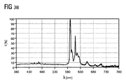
図2は、蛍光体の発光スペクトルを示し、ここで、nmで示される波長λに依存する、パーセントで示される強度Iが示される。この蛍光体は、実施例A3により製造した。この蛍光体は、おそらく、組成(Sr1-aEua)3-x(AlbSi1-b)2(OcN1-c)6-yを示し、ここで0≦a≦1及び0≦b≦1及び0≦c≦1及びx≦3及びy≦6である。電磁一次放射線による励起は、460nmで行った。この発光スペクトルから、この蛍光体は、約110nmの半値幅で707nmの発光極大を有することが認識できた。 FIG. 2 shows the emission spectrum of the phosphor, where the intensity I in percent is shown, depending on the wavelength λ in nm. This phosphor was manufactured according to Example A3. This phosphor probably exhibits the composition (Sr 1-a Eu a ) 3-x (Al b Si 1-b ) 2 (O c N 1-c ) 6-y , where 0 ≦ a ≦ 1 and 0 ≦ b ≦ 1, 0 ≦ c ≦ 1, x ≦ 3 and y ≦ 6. Excitation with electromagnetic primary radiation was performed at 460 nm. From this emission spectrum, it was recognized that this phosphor had an emission maximum of 707 nm with a half width of about 110 nm.
図3aは、比較例Sr3-xAl2+xO6:Eu2+(ここで、aについてx=0.05、bについてx=0.2、cについてx=0.3及びdについてx=0.4)の比較される発光スペクトルa〜dを示し、ここで、nmで示される波長ラムダに依存する、a.U.(任意単位)で示される強度Iが示される。この励起は365nmで行った。同様に、この図は、比較例Sr3-xAl2+xO6:Eu3+(ここで、1−aについてx=0.05、1−bについてx=0.2、1−cについてx=0.3及び1−dについてx=0.4)の発光スペクトルを示し、ここで、励起は254nmで行った。この図中で2つの発光波長が挙げられている。Eu2+発光について(広帯域)365nmで励起した。更に、図3aは、比較例Sr3-xAl2+xO6:Eu2+のxに依存するルミネッセンスのa.U.(任意単位)で示される相対強度を示す。比較例Sr3-xAl2+xO6:Eu2+の発光極大は、365nmの励起で、半値幅70〜80nmで、約525nmである。Eu3+発光の発光極大は、図3aによると約590nmである。この全ての発光スペクトルは、比較例Sr3-xAl2+xO6:Eu2+が、630nm以下の発光極大を有することを示す。
FIG. 3a shows a comparative example Sr 3-x Al 2 + x O 6 : Eu 2+ where x = 0.05 for a, x = 0.2 for b, x = 0.3 for c and d x = 0.4) showing the emission spectra a to d compared, depending on the wavelength lambda denoted in nm, a. U. The intensity I indicated by (arbitrary unit) is indicated. This excitation was performed at 365 nm. Likewise, this figure, Comparative Example Sr 3-x Al 2 + x O 6:
図3bは、比較例Sr3Al2O6:Eu3+の発光スペクトルを示す。比較例Sr3Al2O6:Eu3+の発光極大は、約590nmである。 FIG. 3b shows the emission spectrum of the comparative example Sr 3 Al 2 O 6 : Eu 3+ . Comparative Example Sr 3 Al 2 O 6 : Eu 3+ has an emission maximum of about 590 nm.
従って、蛍光体(図2)は、比較例(Sr1-xEux)3Al2O6(図3a及び3b)と比較して、明らかに赤色方向にシフトした波長領域を示し、より大きな半値幅を有する。このような赤色方向へのシフトは、蛍光体中でのAl−OのSi−Nへの置き換えによって生じたと想定される。同様に、Sr位置での欠損が予想される。これは、結晶格子中でSr位置が完全には占められていないため、結晶格子中での空格子が存在することを意味する。この蛍光体の構造は、Sr3Al2O6(
図3cは、[AlO2O2/2]6 6-単位の空間配置(左側)及び比較例Sr3Al2O6の単位格子(右側)を示す。Sr3Al2O6の場合に、6つの[AlO2O2/2]6 6-四面体からなる単離された環が存在する。 FIG. 3c shows the spatial arrangement of [AlO 2 O 2/2 ] 6 6- units (left side) and the unit cell (right side) of the comparative example Sr 3 Al 2 O 6 . In the case of Sr 3 Al 2 O 6 , there are isolated rings consisting of six [AlO 2 O 2/2 ] 6 6 -tetrahedra.
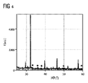
図4は、°で示された2Θの関数としての、%で示された強度Iを有する蛍光体のX線回折図を示す。角度2Θは、ここで及び以後、放射源、プローブ及び検出器の間の角度を表す。この蛍光体は、構造的にSr3Al2O6(
図5は、発光ダイオード(LED)の実施例に関するオプトエレクトロニクス素子の側面図を示す。このオプトエレクトロニクス素子は、活性領域(正確には図示されていない)を備えた層系1、第1の電気接続部2、第2の電気接続部3、ボンディングワイヤ4,注型材5、ハウジング壁部7、ハウジング8、凹所9、蛍光体6、及びマトリックス材料10を有する。蛍光体6を有する、活性領域を備えた層系1は、オプトエレクトロニクス素子内、注型材5及び/又は凹所9の内部に配置されている。この第1及び第2の電気接続部2,3は、活性領域を備えた層系1の下方に配置されている。間接的及び/又は直接的な電気接続及び/又は機械接続は、活性領域を備えた層系1、及びボンディングワイヤ4、及び第1及び/又は第2の電気接続部2,3を備えた活性領域を備えた層系1を有する。
FIG. 5 shows a side view of an optoelectronic device for a light emitting diode (LED) embodiment. This optoelectronic element comprises a
更に、活性領域を備えた層系1は、支持体(ここでは図示されていない)上に配置されていてもよい。支持体は、例えばプリント配線板(PCB)、セラミック支持体、導体プレート又は金属プレート、例えばアルミニウムプレートであることができる。これとは別に、いわゆる薄層型チップの場合に、層系1の支持体なしの配置も可能である。この活性領域は、放射方向へ電磁一次放射線を発するために適している。活性領域を備えた層系1は、例えば窒化物系化合物半導体材料を基礎とすることができる。窒化物系化合物半導体は、特に青色及び/又は紫外のスペクトル領域で電磁一次放射線を発する。特に、窒化物系化合物半導体として、460nmの波長を有する電磁一次放射線を示す、InGaNを使用することができる。
Furthermore, the
電磁一次放射線の光路中に蛍光体6が配置されていて、ここで示されているように、この蛍光体6は粒子形状で存在し、かつマトリックス材料10内に埋め込まれている。このマトリックス材料10は、例えばポリマー材料又はセラミック材料である。この場合、蛍光体6は、直接機械的接続及び/又は電気的接続する形で活性領域を備えた層系1上に配置されている。
A
これとは別に、他の層及び材料、例えば注型材が蛍光体6と層系1との間に配置されていてもよい(ここでは図示されていない)。
Alternatively, other layers and materials, such as casting materials, may be arranged between the
これとは別に、蛍光体6は、ハウジング8のハウジング壁部7に間接的又は直接的に配置されていてもよい(ここでは図示されていない)。
Alternatively, the
これとは別に、蛍光体6が注型材料中に埋め込まれていて(ここでは図示されていない)かつ注型材5としてのマトリックス材料10と一緒に形成されていることも可能である。
Alternatively, the
この蛍光体6は、電磁一次放射線を少なくとも部分的に電磁二次放射線に変換する。例えば、この電磁放射線の青色スペクトル領域の電磁一次放射線を発光し、ここで、この電磁一次放射線の少なくとも一部を蛍光体6によって、電磁放射線の赤色スペクトル領域の電磁二次放射線に変換することができる。これとは別に又は付加的に、例えば緑色スペクトル領域の他の電磁二次放射線を示す他の蛍光体が存在していてもよい。このオプトエレクトロニクス素子から発せられる全体の放射線は、青色に発光する一次放射線と赤色及び緑色に発光する二次放射線とからの重なりであり、この場合、外部の観察者にとって可視の全体の発光は暖白色光である。
This
本発明は、実施例に基づくこの記載により制限されない。むしろ、本発明は、全ての新規の特徴並びにこれらの特徴の全ての組み合わせを有し、これは、特に、これらの特徴又はその組合せ自体が特許請求の範囲又は実施例に明確には記載されていない場合であっても、特許請求の範囲の特徴の全ての組合せを内容とする。 The invention is not limited by this description based on the examples. Rather, the invention has all the novel features as well as all combinations of these features, which in particular are explicitly described in the claims or examples. Even if not, all combinations of the features of the claims are included.
この特許出願は、ドイツ国特許出願第10 2013 105 056.5号の優先権を主張し、その開示内容は、参照により援用される。 This patent application claims the priority of German Patent Application No. 10 2013 105 056.5, the disclosure of which is incorporated by reference.
Claims (16)
A) 出発物質の混合物を製造する工程、
− ここで、前記出発物質は、第1の成分と、第2の成分とを有し、
− ここで、第1の成分は、次の:
− 周期表の第2主族の少なくとも1つの元素、ここで、第1の成分中の第2主族の元素の割合は、45モル%以上でかつ85モル%以下であり、
− アルミニウム、ここで、第1の成分中のアルミニウムの割合は、0モル%以上でかつ40モル%以下であり、
− ケイ素、ここで、第1の成分中のケイ素の割合は、0モル%以上でかつ35モル%以下であり、
− ランタノイドの少なくとも1つの元素及び/又はMn2+及び/又はMn4+、ここで、第1の成分中の、ランタノイドの元素及び/又はMn2+及び/又はMn4+の割合は、0.001モル%以上でかつ20モル%以下である、
を有するか又はこれらからなり、
− ここで、第2の成分は、次の:
− 酸素、ここで、第2の成分中の酸素の割合は、0モル%以上でかつ100モル%以下であり、
− 窒素、ここで、第2の成分中の窒素の割合は、0モル%以上でかつ100モル%以下である
を有するか又はこれらかなり、
B) 前記混合物を、少なくとも1300℃の温度で、還元雰囲気下で焼成する工程、
− ここで、前記方法工程B)により、少なくとも1種以上の相が得られ、
− ここで、少なくとも1種の相は蛍光体(6)を有し、
− ここで、前記蛍光体(6)は、UV領域又は青色領域の電磁一次放射線の少なくとも一部を吸収し、かつ660nm以上の発光極大を有する電磁二次放射線を発する、
を有する蛍光体の製造方法。 Method steps:
A) producing a mixture of starting materials,
-Wherein the starting material has a first component and a second component;
-Where the first component is:
At least one element of the second main group of the periodic table, wherein the proportion of the second main group element in the first component is not less than 45 mol% and not more than 85 mol%;
-Aluminum, wherein the proportion of aluminum in the first component is not less than 0 mol% and not more than 40 mol%,
-Silicon, wherein the proportion of silicon in the first component is not less than 0 mol% and not more than 35 mol%;
At least one element of the lanthanoid and / or Mn 2+ and / or Mn 4+ , wherein the proportion of the lanthanoid element and / or Mn 2+ and / or Mn 4+ in the first component is 0 0.001 mol% or more and 20 mol% or less,
Have or consist of
-Where the second component is:
-Oxygen, wherein the proportion of oxygen in the second component is not less than 0 mol% and not more than 100 mol%,
-Nitrogen, wherein the proportion of nitrogen in the second component is greater than or equal to 0 mol% and less than or equal to 100 mol% or substantially
B) firing the mixture at a temperature of at least 1300 ° C. in a reducing atmosphere;
Wherein at least one or more phases are obtained by said method step B),
-Where at least one phase has the phosphor (6),
-Wherein said phosphor (6) absorbs at least part of the electromagnetic primary radiation in the UV or blue region and emits electromagnetic secondary radiation having an emission maximum of 660 nm or more,
The manufacturing method of the fluorescent substance which has this.
− 周期表の第2主族の少なくとも1つの元素、
− アルミニウム及び/又はケイ素、及び
− ランタノイドの少なくとも1つの元素及び/又はMn2+及び/又はMn4+
を有するか又はこれらからなり、
ここで、第2の蛍光体成分は、少なくとも酸素及び/又は窒素を有し、
ここで、前記蛍光体は、UV領域又は青色領域の電磁一次放射線の少なくとも一部を吸収し、かつ660nm以上の発光極大を有する電磁二次放射線を発するように調整されている、蛍光体。 11. The phosphor of claim 10 having a first phosphor component and a second phosphor component, wherein the first phosphor component is:
-At least one element of the second main group of the periodic table,
-Aluminum and / or silicon, and-at least one element of lanthanoids and / or Mn2 + and / or Mn4 +
Have or consist of
Here, the second phosphor component has at least oxygen and / or nitrogen,
Here, the phosphor is adjusted so as to absorb at least a part of the electromagnetic primary radiation in the UV region or the blue region and emit electromagnetic secondary radiation having an emission maximum of 660 nm or more.
(EA1-aLAa)3-x(AlbSi1-b)2(OcN1-c)6-y
[式中、EAは、第2主族の少なくとも1つの元素を表し、LAは、ランタノイドの群からなる少なくとも1つの元素及び/又はMn2+及び/又はMn4+を表し、0≦a≦1及び0≦b≦1及び0≦c≦1及びx≦3及びy≦6である]を有する、請求項11又は12に記載の蛍光体。 The following general composition:
(EA 1-a LA a ) 3-x (Al b Si 1-b ) 2 (O c N 1-c ) 6-y
[Wherein, EA represents at least one element of the second main group, LA represents at least one element of the group of lanthanoids and / or Mn 2+ and / or Mn 4+ , and 0 ≦ a ≦ The phosphor according to claim 11, wherein 1 and 0 ≦ b ≦ 1 and 0 ≦ c ≦ 1 and x ≦ 3 and y ≦ 6.
Applications Claiming Priority (3)
| Application Number | Priority Date | Filing Date | Title |
|---|---|---|---|
| DE102013105056.5 | 2013-05-16 | ||
| DE102013105056.5A DE102013105056A1 (en) | 2013-05-16 | 2013-05-16 | Process for the preparation of a phosphor, phosphor and optoelectronic component |
| PCT/EP2014/058882 WO2014184003A1 (en) | 2013-05-16 | 2014-04-30 | Method for producing a luminescent material, luminescent material and optoelectronic component |
Publications (2)
| Publication Number | Publication Date |
|---|---|
| JP2016523998A true JP2016523998A (en) | 2016-08-12 |
| JP2016523998A5 JP2016523998A5 (en) | 2017-06-22 |
Family
ID=50733022
Family Applications (1)
| Application Number | Title | Priority Date | Filing Date |
|---|---|---|---|
| JP2016513272A Pending JP2016523998A (en) | 2013-05-16 | 2014-04-30 | Phosphor production method, phosphor and optoelectronic device |
Country Status (5)
| Country | Link |
|---|---|
| US (1) | US10174245B2 (en) |
| JP (1) | JP2016523998A (en) |
| CN (1) | CN105209571A (en) |
| DE (2) | DE102013105056A1 (en) |
| WO (1) | WO2014184003A1 (en) |
Families Citing this family (2)
| Publication number | Priority date | Publication date | Assignee | Title |
|---|---|---|---|---|
| DE102019106546A1 (en) * | 2019-03-14 | 2020-09-17 | OSRAM Opto Semiconductors Gesellschaft mit beschränkter Haftung | METHOD FOR MANUFACTURING OPTOELECTRONIC SEMICONDUCTOR COMPONENTS AND OPTOELECTRONIC SEMICONDUCTOR COMPONENTS |
| TWI809087B (en) * | 2019-04-11 | 2023-07-21 | 晶元光電股份有限公司 | Led package |
Citations (7)
| Publication number | Priority date | Publication date | Assignee | Title |
|---|---|---|---|---|
| JP2005226000A (en) * | 2004-02-13 | 2005-08-25 | Shoei Chem Ind Co | Nitride phosphor, manufacturing method of nitride phosphor, white light emitting element and pigment |
| WO2006033418A1 (en) * | 2004-09-22 | 2006-03-30 | National Institute For Materials Science | Phosphor, process for producing the same and luminescence apparatus |
| JP2006206729A (en) * | 2005-01-27 | 2006-08-10 | National Institute For Materials Science | Phosphor, method for preparation of the same, and light emitting implement |
| KR100761865B1 (en) * | 2006-09-19 | 2007-09-28 | 황유신 | Apparatus for heater of water heater |
| JP2008189700A (en) * | 2007-01-31 | 2008-08-21 | Nichia Chem Ind Ltd | Nitride-based fluorescent material, oxynitride-based fluorescent material and light-emitting device produced by using the same |
| JP2009519364A (en) * | 2005-12-13 | 2009-05-14 | オスラム ゲゼルシャフト ミット ベシュレンクテル ハフツング | Luminescent material emitting in red and light source having this type of luminescent material |
| US20120037938A1 (en) * | 2008-11-20 | 2012-02-16 | Daniel Becker | SR2S15N8 Luminous substance emitting red and light source comprising a luminous substance of said king and method for producing the luminous substance |
Family Cites Families (13)
| Publication number | Priority date | Publication date | Assignee | Title |
|---|---|---|---|---|
| JP4165318B2 (en) | 2003-07-16 | 2008-10-15 | 宇部興産株式会社 | Sialon phosphor and method for producing the same |
| JP3837588B2 (en) | 2003-11-26 | 2006-10-25 | 独立行政法人物質・材料研究機構 | Phosphors and light emitting devices using phosphors |
| JP4511885B2 (en) | 2004-07-09 | 2010-07-28 | Dowaエレクトロニクス株式会社 | Phosphor, LED and light source |
| US7671529B2 (en) | 2004-12-10 | 2010-03-02 | Philips Lumileds Lighting Company, Llc | Phosphor converted light emitting device |
| DE112006001722B4 (en) * | 2005-07-01 | 2021-05-06 | National Institute For Materials Science | Phosphor and process for its production and use of the phosphor |
| US7262439B2 (en) * | 2005-11-22 | 2007-08-28 | Lumination Llc | Charge compensated nitride phosphors for use in lighting applications |
| JP5188687B2 (en) * | 2006-07-18 | 2013-04-24 | 昭和電工株式会社 | Phosphor, manufacturing method thereof, and light emitting device |
| DE102007033026A1 (en) | 2007-07-16 | 2009-01-22 | Osram Gesellschaft mit beschränkter Haftung | Phosphor mixture for a discharge lamp and discharge lamp, in particular Hg low-pressure discharge lamp |
| DE102009032711A1 (en) | 2009-07-11 | 2011-01-20 | Merck Patent Gmbh | Co-doped silicooxynitrides |
| WO2011028033A2 (en) | 2009-09-02 | 2011-03-10 | 엘지이노텍주식회사 | Phosphor, preparation method of phosphor, and white light emitting device |
| KR101565988B1 (en) * | 2009-10-23 | 2015-11-05 | 삼성전자주식회사 | Red phosphor Method for preparing the same Light emitting device package and Lighting apparatus using the Red Phosphor |
| KR101164918B1 (en) | 2010-05-27 | 2012-07-19 | 대덕지디에스 주식회사 | Photovoltaic Module And Manufacture Methode Of The Same |
| KR101856534B1 (en) | 2011-12-07 | 2018-05-14 | 삼성전자주식회사 | Oxinitride phosphor and light emitting device comprising the same |
-
2013
- 2013-05-16 DE DE102013105056.5A patent/DE102013105056A1/en not_active Withdrawn
-
2014
- 2014-04-30 DE DE112014002412.0T patent/DE112014002412A5/en not_active Ceased
- 2014-04-30 CN CN201480028408.8A patent/CN105209571A/en active Pending
- 2014-04-30 JP JP2016513272A patent/JP2016523998A/en active Pending
- 2014-04-30 WO PCT/EP2014/058882 patent/WO2014184003A1/en active Application Filing
- 2014-04-30 US US14/891,596 patent/US10174245B2/en not_active Expired - Fee Related
Patent Citations (13)
| Publication number | Priority date | Publication date | Assignee | Title |
|---|---|---|---|---|
| JP2005226000A (en) * | 2004-02-13 | 2005-08-25 | Shoei Chem Ind Co | Nitride phosphor, manufacturing method of nitride phosphor, white light emitting element and pigment |
| US20080143246A1 (en) * | 2004-09-22 | 2008-06-19 | National Institution For Materials Science | Phosphor, Production Method Thereof and Light Emitting Instrument |
| EP1806389A1 (en) * | 2004-09-22 | 2007-07-11 | National Institute for Materials Science | Phosphor, process for producing the same and luminescence apparatus |
| CN101044222A (en) * | 2004-09-22 | 2007-09-26 | 独立行政法人物质·材料研究机构 | Phospher, process for producing the same and luminescence apparatus |
| WO2006033418A1 (en) * | 2004-09-22 | 2006-03-30 | National Institute For Materials Science | Phosphor, process for producing the same and luminescence apparatus |
| JP5105347B2 (en) * | 2004-09-22 | 2012-12-26 | 独立行政法人物質・材料研究機構 | Phosphor, method for producing the same, and light emitting device |
| JP2006206729A (en) * | 2005-01-27 | 2006-08-10 | National Institute For Materials Science | Phosphor, method for preparation of the same, and light emitting implement |
| JP2009519364A (en) * | 2005-12-13 | 2009-05-14 | オスラム ゲゼルシャフト ミット ベシュレンクテル ハフツング | Luminescent material emitting in red and light source having this type of luminescent material |
| US20090212683A1 (en) * | 2005-12-13 | 2009-08-27 | Osram Gesellschaft mit beschränkter Haftung | Red-Emitting Luminescent Substance and Light Source Comprising Such a Luminescent Substance |
| KR100761865B1 (en) * | 2006-09-19 | 2007-09-28 | 황유신 | Apparatus for heater of water heater |
| JP2008189700A (en) * | 2007-01-31 | 2008-08-21 | Nichia Chem Ind Ltd | Nitride-based fluorescent material, oxynitride-based fluorescent material and light-emitting device produced by using the same |
| US20120037938A1 (en) * | 2008-11-20 | 2012-02-16 | Daniel Becker | SR2S15N8 Luminous substance emitting red and light source comprising a luminous substance of said king and method for producing the luminous substance |
| JP2012509373A (en) * | 2008-11-20 | 2012-04-19 | オスラム アクチエンゲゼルシャフト | Red light-emitting Sr2Si5N8 type phosphor, light source having such phosphor, and method for producing the phosphor |
Also Published As
| Publication number | Publication date |
|---|---|
| US20160122637A1 (en) | 2016-05-05 |
| US10174245B2 (en) | 2019-01-08 |
| DE112014002412A5 (en) | 2016-02-04 |
| CN105209571A (en) | 2015-12-30 |
| DE102013105056A1 (en) | 2014-11-20 |
| WO2014184003A1 (en) | 2014-11-20 |
Similar Documents
| Publication | Publication Date | Title |
|---|---|---|
| US10711191B2 (en) | Phosphor, method for producing a phosphor and use of a phosphor | |
| JP5234781B2 (en) | Phosphor, method for producing the same, and light emitting device | |
| KR101539446B1 (en) | Green-emitting, garnet-based phosphors in general and backlighting applications | |
| JP5190475B2 (en) | Phosphor and light emitting device using the same | |
| JP5944508B2 (en) | Optoelectronic parts | |
| JP5224439B2 (en) | Phosphor and light emitting device using the same | |
| US9331253B2 (en) | Light emitting diode (LED) component comprising a phosphor with improved excitation properties | |
| Han et al. | New full-color-emitting phosphor, Eu 2+-doped Na 2− x Al 2− x Si x O 4 (0≤ x≤ 1), obtained using phase transitions for solid-state white lighting | |
| TWI448536B (en) | Yellow-green to yellow-emitting phosphors based on halogenated-aluminates | |
| JP4733535B2 (en) | Oxynitride phosphor, method for manufacturing oxynitride phosphor, semiconductor light emitting device, light emitting device, light source, illumination device, and image display device | |
| Bispo et al. | Red phosphor based on Eu 3+-isoelectronically doped Ba 2 SiO 4 obtained via sol–gel route for solid state lightning | |
| JP2008024741A (en) | Phosphor, its manufacturing method and light emitting device | |
| JP6181292B2 (en) | Method for producing powdery precursor material, powdery precursor material and method of use thereof | |
| JPWO2016186057A1 (en) | Phosphor, method for manufacturing the same, lighting apparatus, and image display device | |
| KR101789856B1 (en) | Blue-light-emitting phosphor and light-emitting device equipped with the blue-light-emitting phosphor | |
| TWI438263B (en) | Strontium oxyorthosilicate phosphors having improved stability under a radiation load and resistance to atmospheric humidity | |
| JPWO2016186058A1 (en) | Luminescent fixture and image display device | |
| JP2016216711A (en) | Phosphor, production method of the same, lighting apparatus and image display device | |
| JP6143949B2 (en) | Method for producing powdery precursor material, powdery precursor material and method of use thereof | |
| JP4899433B2 (en) | Phosphor, and light emitting device, image display device, and illumination device using the same | |
| JP2012531488A (en) | Luminescent material with Eu2 + -doped silicate phosphor | |
| US11453821B2 (en) | Narrow band emitting SiAlON phosphor | |
| JP5071714B2 (en) | Phosphor, method for producing the same, and light emitting device using the same | |
| JP2016523998A (en) | Phosphor production method, phosphor and optoelectronic device | |
| TWI394827B (en) | Phosphors and white light illumination devices utilizing the same |
Legal Events
| Date | Code | Title | Description |
|---|---|---|---|
| A977 | Report on retrieval |
Free format text: JAPANESE INTERMEDIATE CODE: A971007 Effective date: 20161130 |
|
| A131 | Notification of reasons for refusal |
Free format text: JAPANESE INTERMEDIATE CODE: A131 Effective date: 20170130 |
|
| A524 | Written submission of copy of amendment under article 19 pct |
Free format text: JAPANESE INTERMEDIATE CODE: A524 Effective date: 20170428 |
|
| A02 | Decision of refusal |
Free format text: JAPANESE INTERMEDIATE CODE: A02 Effective date: 20171002 |