JP2016196675A - Vapor deposition mask production method - Google Patents
Vapor deposition mask production method Download PDFInfo
- Publication number
- JP2016196675A JP2016196675A JP2015076129A JP2015076129A JP2016196675A JP 2016196675 A JP2016196675 A JP 2016196675A JP 2015076129 A JP2015076129 A JP 2015076129A JP 2015076129 A JP2015076129 A JP 2015076129A JP 2016196675 A JP2016196675 A JP 2016196675A
- Authority
- JP
- Japan
- Prior art keywords
- vapor deposition
- deposition mask
- opening
- hole
- metal layer
- Prior art date
- Legal status (The legal status is an assumption and is not a legal conclusion. Google has not performed a legal analysis and makes no representation as to the accuracy of the status listed.)
- Granted
Links
- 238000007740 vapor deposition Methods 0.000 title claims abstract description 244
- 238000004519 manufacturing process Methods 0.000 title claims abstract description 46
- 230000001678 irradiating effect Effects 0.000 claims abstract description 13
- 238000002360 preparation method Methods 0.000 claims abstract description 7
- 238000001514 detection method Methods 0.000 claims abstract description 6
- 229910052751 metal Inorganic materials 0.000 claims description 154
- 239000002184 metal Substances 0.000 claims description 154
- 238000000034 method Methods 0.000 claims description 97
- 239000000758 substrate Substances 0.000 claims description 68
- 238000007747 plating Methods 0.000 claims description 67
- 239000000463 material Substances 0.000 claims description 58
- 238000005530 etching Methods 0.000 claims description 41
- 238000000151 deposition Methods 0.000 claims description 33
- 230000008021 deposition Effects 0.000 claims description 31
- PXHVJJICTQNCMI-UHFFFAOYSA-N Nickel Chemical compound [Ni] PXHVJJICTQNCMI-UHFFFAOYSA-N 0.000 claims description 18
- 229910052759 nickel Inorganic materials 0.000 claims description 9
- 229910000640 Fe alloy Inorganic materials 0.000 claims description 8
- 238000000926 separation method Methods 0.000 claims description 5
- 238000002955 isolation Methods 0.000 claims description 2
- 239000000243 solution Substances 0.000 description 44
- 238000010586 diagram Methods 0.000 description 14
- 229920005989 resin Polymers 0.000 description 12
- 239000011347 resin Substances 0.000 description 12
- 230000015572 biosynthetic process Effects 0.000 description 8
- 238000005019 vapor deposition process Methods 0.000 description 8
- 238000009713 electroplating Methods 0.000 description 6
- 238000012986 modification Methods 0.000 description 6
- 230000004048 modification Effects 0.000 description 6
- 239000003054 catalyst Substances 0.000 description 5
- VEXZGXHMUGYJMC-UHFFFAOYSA-N Hydrochloric acid Chemical compound Cl VEXZGXHMUGYJMC-UHFFFAOYSA-N 0.000 description 4
- 230000002950 deficient Effects 0.000 description 4
- 238000007772 electroless plating Methods 0.000 description 4
- 239000000203 mixture Substances 0.000 description 4
- 230000002093 peripheral effect Effects 0.000 description 4
- 239000013078 crystal Substances 0.000 description 3
- 230000007423 decrease Effects 0.000 description 3
- 238000013461 design Methods 0.000 description 3
- 238000011161 development Methods 0.000 description 3
- 230000003628 erosive effect Effects 0.000 description 3
- 238000007689 inspection Methods 0.000 description 3
- 230000000149 penetrating effect Effects 0.000 description 3
- RYGMFSIKBFXOCR-UHFFFAOYSA-N Copper Chemical compound [Cu] RYGMFSIKBFXOCR-UHFFFAOYSA-N 0.000 description 2
- 229910001374 Invar Inorganic materials 0.000 description 2
- 229910021578 Iron(III) chloride Inorganic materials 0.000 description 2
- OFOBLEOULBTSOW-UHFFFAOYSA-N Malonic acid Chemical compound OC(=O)CC(O)=O OFOBLEOULBTSOW-UHFFFAOYSA-N 0.000 description 2
- NIXOWILDQLNWCW-UHFFFAOYSA-N acrylic acid group Chemical group C(C=C)(=O)O NIXOWILDQLNWCW-UHFFFAOYSA-N 0.000 description 2
- 239000004020 conductor Substances 0.000 description 2
- 229910052802 copper Inorganic materials 0.000 description 2
- 239000010949 copper Substances 0.000 description 2
- 239000011521 glass Substances 0.000 description 2
- 238000010438 heat treatment Methods 0.000 description 2
- RBTARNINKXHZNM-UHFFFAOYSA-K iron trichloride Chemical compound Cl[Fe](Cl)Cl RBTARNINKXHZNM-UHFFFAOYSA-K 0.000 description 2
- 239000007769 metal material Substances 0.000 description 2
- 239000011259 mixed solution Substances 0.000 description 2
- 230000003287 optical effect Effects 0.000 description 2
- 239000011368 organic material Substances 0.000 description 2
- 230000010355 oscillation Effects 0.000 description 2
- 238000000059 patterning Methods 0.000 description 2
- VYZAMTAEIAYCRO-UHFFFAOYSA-N Chromium Chemical compound [Cr] VYZAMTAEIAYCRO-UHFFFAOYSA-N 0.000 description 1
- 229910000531 Co alloy Inorganic materials 0.000 description 1
- 229910052779 Neodymium Inorganic materials 0.000 description 1
- QXZUUHYBWMWJHK-UHFFFAOYSA-N [Co].[Ni] Chemical compound [Co].[Ni] QXZUUHYBWMWJHK-UHFFFAOYSA-N 0.000 description 1
- 239000000654 additive Substances 0.000 description 1
- 229910052782 aluminium Inorganic materials 0.000 description 1
- XAGFODPZIPBFFR-UHFFFAOYSA-N aluminium Chemical compound [Al] XAGFODPZIPBFFR-UHFFFAOYSA-N 0.000 description 1
- 229910017052 cobalt Inorganic materials 0.000 description 1
- 239000010941 cobalt Substances 0.000 description 1
- GUTLYIVDDKVIGB-UHFFFAOYSA-N cobalt atom Chemical compound [Co] GUTLYIVDDKVIGB-UHFFFAOYSA-N 0.000 description 1
- 239000003086 colorant Substances 0.000 description 1
- 230000007547 defect Effects 0.000 description 1
- 239000000428 dust Substances 0.000 description 1
- 238000001704 evaporation Methods 0.000 description 1
- 230000008020 evaporation Effects 0.000 description 1
- 239000002223 garnet Substances 0.000 description 1
- 238000009413 insulation Methods 0.000 description 1
- 150000002506 iron compounds Chemical class 0.000 description 1
- SQZYOZWYVFYNFV-UHFFFAOYSA-L iron(2+);disulfamate Chemical compound [Fe+2].NS([O-])(=O)=O.NS([O-])(=O)=O SQZYOZWYVFYNFV-UHFFFAOYSA-L 0.000 description 1
- 238000005304 joining Methods 0.000 description 1
- 238000010030 laminating Methods 0.000 description 1
- 239000007788 liquid Substances 0.000 description 1
- QEFYFXOXNSNQGX-UHFFFAOYSA-N neodymium atom Chemical compound [Nd] QEFYFXOXNSNQGX-UHFFFAOYSA-N 0.000 description 1
- 150000002816 nickel compounds Chemical class 0.000 description 1
- KERTUBUCQCSNJU-UHFFFAOYSA-L nickel(2+);disulfamate Chemical compound [Ni+2].NS([O-])(=O)=O.NS([O-])(=O)=O KERTUBUCQCSNJU-UHFFFAOYSA-L 0.000 description 1
- 230000035515 penetration Effects 0.000 description 1
- 238000000206 photolithography Methods 0.000 description 1
- 229920002120 photoresistant polymer Polymers 0.000 description 1
- 238000001556 precipitation Methods 0.000 description 1
- 238000012545 processing Methods 0.000 description 1
- 230000001737 promoting effect Effects 0.000 description 1
- 230000004043 responsiveness Effects 0.000 description 1
- CVHZOJJKTDOEJC-UHFFFAOYSA-N saccharin Chemical compound C1=CC=C2C(=O)NS(=O)(=O)C2=C1 CVHZOJJKTDOEJC-UHFFFAOYSA-N 0.000 description 1
- 229940081974 saccharin Drugs 0.000 description 1
- 235000019204 saccharin Nutrition 0.000 description 1
- 239000000901 saccharin and its Na,K and Ca salt Substances 0.000 description 1
- 239000000126 substance Substances 0.000 description 1
- 229920003002 synthetic resin Polymers 0.000 description 1
- 239000000057 synthetic resin Substances 0.000 description 1
- 238000012360 testing method Methods 0.000 description 1
- 238000003466 welding Methods 0.000 description 1
- 229910052727 yttrium Inorganic materials 0.000 description 1
- VWQVUPCCIRVNHF-UHFFFAOYSA-N yttrium atom Chemical compound [Y] VWQVUPCCIRVNHF-UHFFFAOYSA-N 0.000 description 1
Images


Classifications
-
- C—CHEMISTRY; METALLURGY
- C23—COATING METALLIC MATERIAL; COATING MATERIAL WITH METALLIC MATERIAL; CHEMICAL SURFACE TREATMENT; DIFFUSION TREATMENT OF METALLIC MATERIAL; COATING BY VACUUM EVAPORATION, BY SPUTTERING, BY ION IMPLANTATION OR BY CHEMICAL VAPOUR DEPOSITION, IN GENERAL; INHIBITING CORROSION OF METALLIC MATERIAL OR INCRUSTATION IN GENERAL
- C23F—NON-MECHANICAL REMOVAL OF METALLIC MATERIAL FROM SURFACE; INHIBITING CORROSION OF METALLIC MATERIAL OR INCRUSTATION IN GENERAL; MULTI-STEP PROCESSES FOR SURFACE TREATMENT OF METALLIC MATERIAL INVOLVING AT LEAST ONE PROCESS PROVIDED FOR IN CLASS C23 AND AT LEAST ONE PROCESS COVERED BY SUBCLASS C21D OR C22F OR CLASS C25
- C23F1/00—Etching metallic material by chemical means
- C23F1/02—Local etching
Abstract
Description
本発明は、複数の貫通孔が形成された蒸着マスクを製造する蒸着マスク製造方法に関する。 The present invention relates to a deposition mask manufacturing method for manufacturing a deposition mask in which a plurality of through holes are formed.
近年、スマートフォンやタブレットPC等の持ち運び可能なデバイスで用いられる表示装置に対して、高精細であること、例えば画素密度が400ppi以上であることが求められている。また、持ち運び可能なデバイスにおいても、ウルトラフルハイビジョンに対応することへの需要が高まっており、この場合、表示装置の画素密度が例えば800ppi以上であることが求められる。 In recent years, a display device used in a portable device such as a smartphone or a tablet PC is required to have high definition, for example, a pixel density of 400 ppi or more. In portable devices, there is an increasing demand for compatibility with ultra full high vision, and in this case, the pixel density of the display device is required to be, for example, 800 ppi or more.
表示装置の中でも、応答性の良さ、消費電力の低さやコントラストの高さのため、有機EL表示装置が注目されている。有機EL表示装置の画素を形成する方法として、所望のパターンで配列された貫通孔を含む蒸着マスクを用い、所望のパターンで画素を形成する方法が知られている。具体的には、はじめに、有機EL表示装置用の基板に対して蒸着マスクを密着させ、次に、密着させた蒸着マスクおよび基板を共に蒸着装置に投入し、有機材料を基板に蒸着させる蒸着工程を行う。この場合、高い画素密度を有する有機EL表示装置を精密に作製するためには、蒸着マスクの貫通孔の位置や形状を設計に沿って精密に再現することが求められる。 Among display devices, organic EL display devices have attracted attention because of their excellent responsiveness, low power consumption, and high contrast. As a method of forming pixels of an organic EL display device, a method of forming pixels with a desired pattern using a vapor deposition mask including through holes arranged in a desired pattern is known. Specifically, first, a deposition mask is brought into intimate contact with a substrate for an organic EL display device, and then the deposited deposition mask and the substrate are both put into a deposition apparatus to deposit an organic material on the substrate. I do. In this case, in order to precisely manufacture an organic EL display device having a high pixel density, it is required to accurately reproduce the position and shape of the through hole of the vapor deposition mask according to the design.
蒸着マスクの製造方法としては、例えば特許文献1に開示されているように、フォトリソグラフィー技術を用いたエッチングによって金属板に貫通孔を形成する方法が知られている。例えば、はじめに、金属板の第1面上に第1レジストパターンを形成し、また金属板の第2面上に第2レジストパターンを形成する。次に、金属板の第1面のうち第1レジストパターンによって覆われていない領域をエッチングして、金属板の第1面に第1開口部を形成する。その後、金属板の第2面のうち第2レジストパターンによって覆われていない領域をエッチングして、金属板の第2面に第2開口部を形成する。この際、第1開口部と第2開口部とが通じ合うようにエッチングを行うことにより、金属板を貫通する貫通孔を形成することができる。
As a method for manufacturing a vapor deposition mask, for example, as disclosed in
その他にも、蒸着マスクの製造方法として、例えば特許文献2に開示されているように、めっき処理を利用して蒸着マスクを製造する方法が知られている。例えば特許文献2に記載の方法においては、はじめに、導電性を有する基材を準備する。次に、基材の上に、所定の隙間を空けてレジストパターンを形成する。このレジストパターンは、蒸着マスクの貫通孔が形成されるべき位置に設けられている。その後、レジストパターンの隙間にめっき液を供給して、電解めっき処理によって基材の上に金属層を析出させる。その後、金属層を基材から分離させることにより、複数の貫通孔が形成された蒸着マスクを得ることができる。
In addition, as a method for manufacturing a vapor deposition mask, for example, as disclosed in
上述のように、高い画素密度を有する有機EL表示装置を精密に作製するためには、蒸着マスクの貫通孔の位置や形状を設計に沿って精密に再現することが求められる。しかしながら、特許文献1のようにエッチングによって貫通孔を形成する場合、エッチング速度やエッチング時間のばらつき、エッチングの間に金属板に付着する異物や、金属板上に設けられているレジストパターンの位置の誤差などに起因して、蒸着マスクのうち貫通孔が形成されるべき部分に貫通孔が正確に形成されない、という事態が生じ得る。例えば、形成されるべき貫通孔の寸法よりも小さな貫通孔が金属板に形成されるという事態、すなわち、金属板のうちエッチングで除去されるべき部分が除去されずに不要部分として残る、という事態が生じ得る。このような不要部分が存在している蒸着マスクは、検査工程において不良品と判定されて廃棄される。従って、上述のような不要部分が残ることは、蒸着マスクの製造の歩留りを低下させてしまう。
As described above, in order to precisely manufacture an organic EL display device having a high pixel density, it is required to accurately reproduce the position and shape of the through hole of the vapor deposition mask according to the design. However, when the through-hole is formed by etching as in
金属板上に設けられているレジストパターンの位置に誤差が生じる原因としては、例えば、レジスト膜を露光する際に用いられる露光マスクの遮光部の形状の誤差が考えられる。露光マスクの遮光部の形状に誤差が生じる原因としては、露光マスクの遮光部が他の部材との接触などによって損傷することなどが考えられる。また、レジストパターンの位置に誤差が生じる原因としては、他にも、露光されたレジスト膜を現像してレジストパターンを形成する現像処理の際の、現像時間の不足が考えられる。 As a cause of an error in the position of the resist pattern provided on the metal plate, for example, an error in the shape of the light shielding portion of the exposure mask used when exposing the resist film can be considered. A possible cause of an error in the shape of the light shielding portion of the exposure mask is that the light shielding portion of the exposure mask is damaged due to contact with other members. Another possible cause of an error in the position of the resist pattern is insufficient development time during the development process of developing the exposed resist film to form a resist pattern.
また特許文献2のようにめっき処理によって蒸着マスクを作製する場合にも、以下に説明するように、蒸着マスクに上述の不要部分が存在することが考えられる。
めっき処理を利用する場合、上述のように、基材上に形成されるレジストパターンは、蒸着マスクの貫通孔が形成されるべき位置に配置される。一方、めっき処理工程においては、レジストパターンの隙間に供給されためっき液が、レジストパターンと基材との間に浸入してしまうことが生じ得る。浸入しためっき液がレジストパターンと基材との間で析出すると、貫通孔が形成されるべきであるが貫通孔が形成されていない部分、すなわち不要部分が形成されることになる。このようにめっき処理によって蒸着マスクを作製する場合にも、不要部分が形成されることによって蒸着マスクの製造の歩留りが低下することが考えられる。
不要部分が形成される原因としては、その他にも、めっき処理の際に基材に付着する異物が考えられる。また、後述するように基材上に設けられたレジストパターンの隙間にめっき液を供給して蒸着マスクを作製する場合、レジスト膜を露光するための露光マスクに異物が付着することによって、レジストパターンの位置に誤差が生じ、この結果、めっき処理の際に不要部分が形成されてしまうことが考えられる。
Further, when the vapor deposition mask is produced by plating as in
When utilizing a plating process, as mentioned above, the resist pattern formed on a base material is arrange | positioned in the position where the through-hole of a vapor deposition mask should be formed. On the other hand, in the plating process, the plating solution supplied to the gap between the resist patterns may enter between the resist pattern and the substrate. When the invading plating solution is deposited between the resist pattern and the substrate, a through hole should be formed, but a portion where no through hole is formed, that is, an unnecessary portion is formed. Even when a vapor deposition mask is produced by plating as described above, it is conceivable that the production yield of the vapor deposition mask decreases due to the formation of unnecessary portions.
Another possible cause of the formation of the unnecessary portion is a foreign matter that adheres to the substrate during the plating process. In addition, when a deposition mask is produced by supplying a plating solution to a gap between resist patterns provided on a substrate as will be described later, the resist pattern is formed by foreign matters adhering to the exposure mask for exposing the resist film. It is conceivable that an error occurs in the position, and as a result, an unnecessary portion is formed during the plating process.
本発明は、このような課題を効果的に解決し得る蒸着マスク製造方法を提供することを目的とする。 An object of this invention is to provide the vapor deposition mask manufacturing method which can solve such a subject effectively.
本発明は、蒸着マスク製造方法であって、複数の貫通孔が形成された蒸着マスクを準備する準備工程と、前記蒸着マスクのうち、前記貫通孔が形成されるべきであるが前記貫通孔が形成されていない不要部分を検出する検出工程と、前記不要部分にレーザー光を照射して前記不要部分を除去する除去工程と、を備え、除去工程において前記不要部分に照射される前記レーザー光のスポット径は、形成されるべき貫通孔の寸法よりも小さい、蒸着マスク製造方法である。 The present invention is a vapor deposition mask manufacturing method, comprising: a preparation step of preparing a vapor deposition mask having a plurality of through holes formed therein; and the through holes are to be formed among the vapor deposition masks. A detection step of detecting an unnecessary portion that is not formed, and a removal step of irradiating the unnecessary portion with a laser beam to remove the unnecessary portion, wherein the unnecessary portion is irradiated with the laser light. A spot diameter is a vapor deposition mask manufacturing method smaller than the dimension of the through-hole to be formed.
本発明による蒸着マスク製造方法において、前記不要部分は、ニッケルを含む鉄合金を有し、前記レーザー光は、YAGレーザー装置によって生成されるYAGレーザー光の第3高調波を含んでいてもよい。 In the vapor deposition mask manufacturing method according to the present invention, the unnecessary portion may include an iron alloy containing nickel, and the laser beam may include a third harmonic of a YAG laser beam generated by a YAG laser device.
本発明による蒸着マスク製造方法において、前記蒸着マスクは、前記蒸着マスクを用いて蒸着材料を基板に蒸着させる際に前記基板と対向する第1面と、前記第1面の反対側に位置する第2面と、を含み、前記第2面における前記貫通孔の開口寸法は、前記第1面における前記貫通孔の開口寸法よりも大きく、前記レーザー光は、前記第2面側から前記不要部分に照射されてもよい。 In the vapor deposition mask manufacturing method according to the present invention, the vapor deposition mask includes a first surface facing the substrate when the vapor deposition material is deposited on the substrate using the vapor deposition mask, and a first surface positioned on the opposite side of the first surface. And the opening size of the through hole in the second surface is larger than the opening size of the through hole in the first surface, and the laser beam is directed from the second surface side to the unnecessary portion. It may be irradiated.
本発明による蒸着マスク製造方法において、前記除去工程においては、前記レーザー光のパルスが間欠的に前記不要部分に照射され、前記レーザー光の前記パルスの平均出力は、1.5〜2.0mJの範囲内であり、前記レーザー光の前記パルスの幅は、5〜7nsの範囲内であり、前記レーザー光の前記パルスの周期は、1〜60nsの範囲内であってもよい。 In the vapor deposition mask manufacturing method according to the present invention, in the removing step, the unnecessary portion is intermittently irradiated with the pulse of the laser beam, and the average output of the pulse of the laser beam is 1.5 to 2.0 mJ. Within the range, the pulse width of the laser light may be within a range of 5 to 7 ns, and the period of the pulse of the laser light may be within a range of 1 to 60 ns.
本発明による蒸着マスク製造方法において、前記準備工程は、所定の基材上に、所定の隙間を空けてレジストパターンを形成するレジスト形成工程と、前記レジストパターンの前記隙間において金属層を析出させるめっき処理工程と、前記金属層を前記基材から分離させる分離工程と、を有していてもよい。 In the vapor deposition mask manufacturing method according to the present invention, the preparation step includes a resist formation step of forming a resist pattern with a predetermined gap on a predetermined substrate, and plating for depositing a metal layer in the gap of the resist pattern. You may have a process process and the isolation | separation process which isolate | separates the said metal layer from the said base material.
本発明による蒸着マスク製造方法において、前記準備工程は、金属板を準備する工程と、前記金属板上に、所定の隙間を空けてレジストパターンを形成するレジスト形成工程と、前記金属板のうち前記レジストパターンによって覆われていない領域をエッチングして、前記金属板に前記貫通孔を形成する工程と、を有していてもよい。 In the deposition mask manufacturing method according to the present invention, the preparation step includes a step of preparing a metal plate, a resist formation step of forming a resist pattern on the metal plate with a predetermined gap, and the metal plate among the metal plate. Etching a region not covered with a resist pattern to form the through hole in the metal plate.
本発明によれば、貫通孔が形成されるべきであるが貫通孔が形成されていない不要部分が蒸着マスクに存在している場合であっても、不要部分にレーザー光を照射することにより、不要部分を除去することができる。このため、蒸着マスクが不良品と判定されてしまうことを抑制することができる。 According to the present invention, even if an unnecessary portion where a through hole should be formed but no through hole is present in the vapor deposition mask, by irradiating the unnecessary portion with laser light, Unnecessary portions can be removed. For this reason, it can suppress that a vapor deposition mask will be determined to be inferior goods.
以下、図面を参照して本発明の一実施の形態について説明する。なお、本件明細書に添付する図面においては、図示と理解のしやすさの便宜上、適宜縮尺および縦横の寸法比等を、実物のそれらから変更し誇張してある。 Hereinafter, an embodiment of the present invention will be described with reference to the drawings. In the drawings attached to the present specification, for the sake of illustration and ease of understanding, the scale, the vertical / horizontal dimension ratio, and the like are appropriately changed and exaggerated from those of the actual product.
図1〜図11は、本発明による一実施の形態およびその変形例を説明するための図である。以下の実施の形態およびその変形例では、有機EL表示装置を製造する際に有機材料を所望のパターンで基板上にパターニングするために用いられる蒸着マスクの製造方法を例にあげて説明する。ただし、このような適用に限定されることなく、種々の用途に用いられる蒸着マスクの製造方法に対し、本発明を適用することができる。 FIGS. 1-11 is a figure for demonstrating one Embodiment and its modification by this invention. In the following embodiments and modifications thereof, a method for manufacturing a vapor deposition mask used for patterning an organic material on a substrate in a desired pattern when manufacturing an organic EL display device will be described as an example. However, the present invention can be applied to a method of manufacturing a vapor deposition mask used for various purposes without being limited to such application.
なお、本明細書において、「板」、「シート」、「フィルム」の用語は、呼称の違いのみに基づいて、互いから区別されるものではない。例えば、「板」はシートやフィルムと呼ばれ得るような部材も含む概念である。 In the present specification, the terms “plate”, “sheet”, and “film” are not distinguished from each other only based on the difference in names. For example, the “plate” is a concept including a member that can be called a sheet or a film.
また、「板面(シート面、フィルム面)」とは、対象となる板状(シート状、フィルム状)の部材を全体的かつ大局的に見た場合において対象となる板状部材(シート状部材、フィルム状部材)の平面方向と一致する面のことを指す。また、板状(シート状、フィルム状)の部材に対して用いる法線方向とは、当該部材の板面(シート面、フィルム面)に対する法線方向のことを指す。 In addition, “plate surface (sheet surface, film surface)” means a target plate-like member (sheet-like) when the target plate-like (sheet-like, film-like) member is viewed as a whole and globally. It refers to the surface that coincides with the plane direction of the member or film-like member. Moreover, the normal direction used with respect to a plate-shaped (sheet-like, film-like) member refers to the normal direction with respect to the plate surface (sheet surface, film surface) of the member.
さらに、本明細書において用いる、形状や幾何学的条件および物理的特性並びにそれらの程度を特定する、例えば、「平行」、「直交」、「同一」、「同等」等の用語や長さや角度並びに物理的特性の値等については、厳密な意味に縛られることなく、同様の機能を期待し得る程度の範囲を含めて解釈することとする。 Further, as used herein, the shape, geometric conditions and physical characteristics and their degree are specified, for example, terms such as “parallel”, “orthogonal”, “identical”, “equivalent”, lengths and angles In addition, values of physical characteristics and the like are not limited to a strict meaning and are interpreted to include a range where a similar function can be expected.
(蒸着マスク装置)
まず、蒸着マスクを含む蒸着マスク装置の一例について、図1〜図3を参照して説明する。ここで、図1は、蒸着マスクを含む蒸着マスク装置の一例を示す平面図であり、図2は、図1に示す蒸着マスク装置の使用方法を説明するための図である。図3は、蒸着マスクを第1面の側から示す平面図である。
(Deposition mask device)
First, an example of a vapor deposition mask apparatus including a vapor deposition mask will be described with reference to FIGS. Here, FIG. 1 is a plan view showing an example of a vapor deposition mask device including a vapor deposition mask, and FIG. 2 is a diagram for explaining a method of using the vapor deposition mask device shown in FIG. FIG. 3 is a plan view showing the vapor deposition mask from the first surface side.
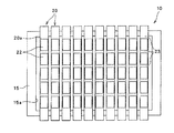
図1及び図2に示された蒸着マスク装置10は、平面視において略矩形状の形状を有する複数の蒸着マスク20と、複数の蒸着マスク20の周縁部に取り付けられたフレーム15と、を備えている。各蒸着マスク20には、蒸着マスク20を貫通する複数の貫通孔25が設けられている。この蒸着マスク装置10は、図2に示すように、蒸着マスク20が蒸着対象物である基板、例えば有機EL基板92の下面に対面するようにして蒸着装置90内に支持され、有機EL基板92への蒸着材料の蒸着に使用される。
The vapor
蒸着装置90内では、不図示の磁石からの磁力によって、蒸着マスク20と有機EL基板92とが密着するようになる。蒸着装置90内には、蒸着マスク装置10の下方に、蒸着材料(一例として、有機発光材料)98を収容するるつぼ94と、るつぼ94を加熱するヒータ96とが配置されている。るつぼ94内の蒸着材料98は、ヒータ96からの加熱により、気化または昇華して有機EL基板92の表面に付着するようになる。上述したように、蒸着マスク20には多数の貫通孔25が形成されており、蒸着材料98はこの貫通孔25を介して有機EL基板92に付着する。この結果、蒸着マスク20の貫通孔25の位置に対応した所望のパターンで、蒸着材料98が有機EL基板92の表面に成膜される。図2において、蒸着マスク20の面のうち蒸着工程の際に有機EL基板92と対向する面(以下、第1面とも称する)が符号20aで表されている。また、蒸着マスク20の面のうち第1面20aの反対側に位置する面(以下、第2面とも称する)が符号20bで表されている。第2面20b側には、蒸着材料98の蒸着源(ここではるつぼ94)が配置される。
In the
上述したように、本実施の形態では、貫通孔25が各有効領域22において所定のパターンで配置されている。なお、複数の色によるカラー表示を行いたい場合には、各色に対応する蒸着マスク20が搭載された蒸着機をそれぞれ準備し、有機EL基板92を各蒸着機に順に投入する。これによって、例えば、赤色用の有機発光材料、緑色用の有機発光材料および青色用の有機発光材料を順に有機EL基板92に蒸着させることができる。
As described above, in the present embodiment, the through
なお、蒸着マスク装置10のフレーム15は、矩形状の蒸着マスク20の周縁部に取り付けられている。フレーム15は、蒸着マスク20が撓んでしまうことがないように蒸着マスク20を張った状態に保持する。蒸着マスク20とフレーム15とは、例えばスポット溶接により互いに対して固定されている。
The
ところで蒸着処理は、高温雰囲気となる蒸着装置90の内部で実施される場合がある。この場合、蒸着処理の間、蒸着装置90の内部に保持される蒸着マスク20、フレーム15および有機EL基板92も加熱される。この際、蒸着マスク20、フレーム15および有機EL基板92は、各々の熱膨張係数に基づいた寸法変化の挙動を示すことになる。この場合、蒸着マスク20やフレーム15と有機EL基板92の熱膨張係数が大きく異なっていると、それらの寸法変化の差異に起因した位置ずれが生じ、この結果、有機EL基板92上に付着する蒸着材料の寸法精度や位置精度が低下してしまう。このような課題を解決するため、蒸着マスク20およびフレーム15の熱膨張係数が、有機EL基板92の熱膨張係数と同等の値であることが好ましい。例えば、有機EL基板92としてガラス基板が用いられる場合、蒸着マスク20およびフレーム15の主要な材料として、ニッケルを含む鉄合金を用いることができる。具体的には、34〜38質量%のニッケルを含むインバー材や、ニッケルに加えてさらにコバルトを含むスーパーインバー材などの鉄合金を、蒸着マスク20を構成する後述する第1金属層32および第2金属層37や金属板21の材料として用いることができる。なお本明細書において、「〜」という記号によって表現される数値範囲は、「〜」という符号の前後に置かれた数値を含んでいる。例えば、「34〜38質量%」という表現によって画定される数値範囲は、「34質量%以上かつ38質量%以下」という表現によって画定される数値範囲と同一である。
By the way, a vapor deposition process may be implemented inside the
なお蒸着処理の際に、蒸着マスク20、フレーム15および有機EL基板92の温度が高温には達しない場合は、蒸着マスク20およびフレーム15の熱膨張係数を有機EL基板92の熱膨張係数と同等の値にする必要は特にない。この場合、蒸着マスク20を構成する後述する第1金属層32および第2金属層37や金属板21の材料として、ニッケルやニッケル−コバルト合金など、上述の鉄合金以外の様々な材料を用いることができる。
In the vapor deposition process, if the temperature of the
(蒸着マスク)
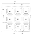
次に、蒸着マスク20について詳細に説明する。図1に示すように、本実施の形態において、蒸着マスク20は、平面視において略四角形形状、さらに正確には平面視において略矩形状の輪郭を有している。蒸着マスク20は、規則的な配列で貫通孔25が形成された有効領域22と、有効領域22を取り囲む周囲領域23と、を含んでいる。周囲領域23は、有効領域22を支持するための領域であり、有機EL基板92へ蒸着されることを意図された蒸着材料が通過する領域ではない。例えば、有機EL表示装置用の有機発光材料の蒸着に用いられる蒸着マスク20においては、有効領域22は、有機発光材料が蒸着して画素を形成するようになる有機EL基板92の表示領域となる区域に対面する、蒸着マスク20内の領域のことである。ただし、種々の目的から、周囲領域23に貫通孔や凹部が形成されていてもよい。図1に示された例において、各有効領域22は、平面視において略四角形形状、さらに正確には平面視において略矩形状の輪郭を有している。なお図示はしないが、各有効領域22は、有機EL基板92の表示領域の形状に応じて、様々な形状の輪郭を有することができる。例えば各有効領域22は、円形状の輪郭を有していてもよい。
(Deposition mask)
Next, the
図示された例において、蒸着マスク20の複数の有効領域22は、蒸着マスク20の長手方向と平行な一方向に沿って所定の間隔を空けて一列に配列されている。図示された例では、一つの有効領域22が一つの有機EL表示装置に対応するようになっている。すなわち、図1に示された蒸着マスク装置10(蒸着マスク20)によれば、多面付蒸着が可能となっている。
In the illustrated example, the plurality of
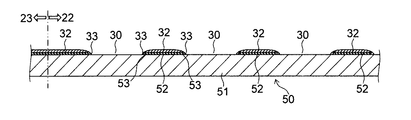
図3に示すように、図示された例において、各有効領域22に形成された複数の貫通孔25は、当該有効領域22において、互いに直交する二方向に沿ってそれぞれ所定のピッチで配列されている。この貫通孔25の形状などについて、以下に詳細に説明する。ここでは、蒸着マスク20がめっき処理またはエッチングによって形成される場合の、貫通孔25の形状などについて、それぞれ説明する。
As shown in FIG. 3, in the illustrated example, the plurality of through
〔形態1 めっき処理によって作製された蒸着マスク〕
はじめに、蒸着マスク20がめっき処理によって作製されたものである場合について説明する。図4は、めっき処理によって作製された蒸着マスク20を、図3のA−A線に沿って切断した場合を示す断面図である。
[
First, the case where the
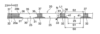
図4に示すように、蒸着マスク20は、所定のパターンで第1開口部30が設けられた第1金属層32と、第1開口部30に連通する第2開口部35が設けられた第2金属層37と、を備えている。第2金属層37は、第1金属層32よりも蒸着マスク20の第2面20b側に配置されている。図4に示す例においては、第1金属層32が蒸着マスク20の第1面20aを構成し、第2金属層37が蒸着マスク20の第2面20bを構成している。
As shown in FIG. 4, the
本実施の形態においては、第1開口部30と第2開口部35とが互いに連通することにより、蒸着マスク20を貫通する貫通孔25が構成されている。この場合、蒸着マスク20の第1面20a側における貫通孔25の開口寸法や開口形状は、第1金属層32の第1開口部30によって画定される。一方、蒸着マスク20の第2面20b側における貫通孔25の開口寸法や開口形状は、第2金属層37の第2開口部35によって画定される。言い換えると、貫通孔25には、第1金属層32の第1開口部30によって画定される形状、および、第2金属層37の第2開口部35によって画定される形状の両方が付与されている。
In the present embodiment, the
図3に示すように、貫通孔25を構成する第1開口部30や第2開口部35は、平面視において略多角形状になっていてもよい。ここでは第1開口部30および第2開口部35が、略四角形状、より具体的には略正方形状になっている例が示されている。また図示はしないが、第1開口部30や第2開口部35は、略六角形状や略八角形状など、その他の略多角形状になっていてもよい。なお「略多角形状」とは、多角形の角部が丸められている形状を含む概念である。また図示はしないが、第1開口部30や第2開口部35は、円形状になっていてもよい。また、平面視において第2開口部35が第1開口部30を囲う輪郭を有する限りにおいて、第1開口部30の形状と第2開口部35の形状が相似形になっている必要はない。
As shown in FIG. 3, the
図4において、符号41は、第1金属層32と第2金属層37とが接続される接続部を表している。また符号S0は、第1金属層32と第2金属層37との接続部41における貫通孔25の寸法を表している。なお図4においては、第1金属層32と第2金属層37とが接している例を示したが、これに限られることはなく、第1金属層32と第2金属層37との間にその他の層が介在されていてもよい。例えば、第1金属層32と第2金属層37との間に、第1金属層32上における第2金属層37の析出を促進させるための触媒層が設けられていてもよい。
In FIG. 4,
図4に示すように、第2面20bにおける貫通孔25(第2開口部35)の開口寸法S2は、第1面20aにおける貫通孔25(第1開口部30)の開口寸法S1よりも大きくなっている。以下、このように第1金属層32および第2金属層37を構成することの利点について説明する。
As shown in FIG. 4, the opening dimension S2 of the through hole 25 (second opening 35) in the
蒸着マスク20の第2面20b側から蒸着マスク20に向かって飛来する蒸着材料98は、貫通孔25の第2開口部35および第1開口部30を順に通って有機EL基板92に付着する。有機EL基板92のうち蒸着材料98が付着する領域は、第1面20aにおける貫通孔25の開口寸法S1や開口形状によって主に定められる。ところで、図4において第2面20b側から第1面20aへ向かう矢印で示すように、蒸着材料98は、るつぼ94から有機EL基板92に向けて蒸着マスク20の法線方向Nに沿って移動するだけでなく、蒸着マスク20の法線方向Nに対して大きく傾斜した方向に移動することもある。ここで、仮に第2面20bにおける貫通孔25の開口寸法S2が第1面20aにおける貫通孔25の開口寸法S1と同一であるとすると、蒸着マスク20の法線方向Nに対して大きく傾斜した方向に移動する蒸着材料98の多くは、貫通孔25を通って有機EL基板92に到達するよりも前に、貫通孔25の第2開口部35の壁面36に到達して付着してしまう。従って、蒸着材料98の利用効率を高めるためには、第2開口部35の開口寸法S2を大きくすることが好ましいと言える。
The
図4において、蒸着マスク20の第2面20b側における貫通孔25(第2開口部35)の端部38を通る蒸着材料98の経路であって、有機EL基板92に到達することができる経路のうち、蒸着マスク20の法線方向Nに対してなす角度が最小となる経路が、符号L1で表されている。また、経路L1と蒸着マスク20の法線方向Nとがなす角度が、符号θ1で表されている。斜めに移動する蒸着材料98を、第2開口部35の壁面36に到達させることなく可能な限り有機EL基板92に到達させるためには、角度θ1を大きくすることが有利となる。例えば角度θ1を45°以上にすることが好ましい。
In FIG. 4, the
上述の開口寸法S0,S1,S2は、有機EL表示装置の画素密度や上述の角度θ1の所望値などを考慮して、適切に設定される。例えば、400ppi以上の画素密度の有機EL表示装置を作製する場合、接続部41における貫通孔25の開口寸法S0は、20〜60μmの範囲内に設定され得る。また、第1面20aにおける第1開口部30の開口寸法S1は、10〜50μmの範囲内に設定され、第2面20bにおける第2開口部35の開口寸法S2は、15〜80μmの範囲内に設定され得る。
The above-described opening dimensions S0, S1, and S2 are appropriately set in consideration of the pixel density of the organic EL display device and the desired value of the above-described angle θ1. For example, when an organic EL display device having a pixel density of 400 ppi or more is manufactured, the opening size S0 of the through
次に、図4に示す蒸着マスク20を、めっき処理を利用して製造する方法について説明する。
Next, a method for manufacturing the
(第1成膜工程)
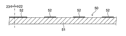
まず図5Aに示すように、所定の導電性パターン52が形成された基材51を準備する。導電性パターン52は、第1金属層32に対応するパターンを有している。絶縁性および適切な強度を有する限りにおいて、基材51を構成する材料や基材51の厚みが特に限られることはない。例えば基材51を構成する材料として、ガラスや合成樹脂などを用いることができる。
(First film formation step)
First, as shown in FIG. 5A, a
導電性パターン52を構成する材料としては、金属材料や酸化物導電性材料等の導電性を有する材料が適宜用いられる。金属材料の例としては、例えばクロムや銅などを挙げることができる。好ましくは、後述するレジストパターン55に対する高い密着性を有する材料が、導電性パターン52を構成する材料として用いられる。例えばレジストパターン55が、アクリル系光硬化性樹脂を含むレジスト膜など、いわゆるドライフィルムと称されるものをパターニングすることによって作製される場合、導電性パターン52を構成する材料として、ドライフィルムに対する高い密着性を有する銅が用いられることが好ましい。
As a material constituting the
後述するように、導電性パターン52の上には、導電性パターン52を覆うように第1金属層32が形成され、この第1金属層32はその後の工程で導電性パターン52から分離される。このため、第1金属層32のうち導電性パターン52と接する側の面の上には、通常、導電性パターン52の厚みに対応する窪みが形成される。この点を考慮すると、電解めっき処理に必要な導電性を導電性パターン52が有する限りにおいて、導電性パターン52の厚みは小さい方が好ましい。例えば導電性パターン52の厚みは、50〜500nmの範囲内になっている。
As will be described later, a
次に、導電性パターン52が形成された基材51上に第1めっき液を供給して、導電性パターン52上に第1金属層32を析出させる第1めっき処理工程を実施する。例えば、導電性パターン52が形成された基材51を、第1めっき液が充填されためっき槽に浸す。これによって、図5Bに示すように、基材51上に、所定のパターンで第1開口部30が設けられた第1金属層32を得ることができる。第1金属層32の厚みは、例えば5μm以下になっている。
Next, a first plating process is performed in which the first plating solution is supplied onto the
なおめっき処理の特性上、図5Bに示すように、第1金属層32は、基材51の法線方向に沿って見た場合に導電性パターン52と重なる部分だけでなく、導電性パターン52と重ならない部分にも形成され得る。これは、導電性パターン52の端部53と重なる部分に析出した第1金属層32の表面にさらに第1金属層32が析出するためである。この結果、図5Bに示すように、第1開口部30の端部33は、基材51の法線方向に沿って見た場合に導電性パターン52と重ならない部分に位置するようになり得る。また端部33の位置は、導電性パターン52の端部53に重なる部分に析出する第1金属層32の析出速度や、第1めっき処理工程が実施される時間(第1めっき処理時間)に応じて変化する。このため、第1金属層32の析出速度や第1めっき処理時間がばらつく場合、端部33の位置にもばらつきが生じ得る。この結果、第1開口部30が形成されるべきであるが第1開口部30が形成されずに第1金属層32が存在している部分(以下、不要部分とも称する)が形成されてしまうことが考えられる。このような課題を解決する方法については、後述する。
Note that, as shown in FIG. 5B, the
導電性パターン52上に第1金属層32を析出させることができる限りにおいて、第1めっき処理工程の具体的な方法が特に限られることはない。例えば第1めっき処理工程は、導電性パターン52に電流を流すことによって導電性パターン52上に第1金属層32を析出させる、いわゆる電解めっき処理工程として実施されてもよい。若しくは、第1めっき処理工程は、無電解めっき処理工程であってもよい。なお第1めっき処理工程が無電解めっき処理工程である場合、導電性パターン52上には適切な触媒層が設けられる。電解めっき処理工程が実施される場合にも、導電性パターン52上に触媒層が設けられていてもよい。
As long as the
用いられる第1めっき液の成分は、第1金属層32に求められる特性に応じて適宜定められる。例えば第1金属層32が、ニッケルを含む鉄合金によって構成される場合、第1めっき液として、ニッケル化合物を含む溶液と、鉄化合物を含む溶液との混合溶液を用いることができる。例えば、スルファミン酸ニッケルを含む溶液と、スルファミン酸鉄を含む溶液との混合溶液を用いることができる。めっき液には、マロン酸やサッカリンなどの添加剤が含まれていてもよい。
The components of the first plating solution used are appropriately determined according to the characteristics required for the
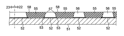
(第2成膜工程)
次に、第1開口部30に連通する第2開口部35が設けられた第2金属層37を第1金属層32上に形成する第2成膜工程を実施する。まず、基材51上および第1金属層32上に、所定の隙間56を空けてレジストパターン55を形成するレジスト形成工程を実施する。図5Cは、基材51上に形成されたレジストパターン55を示す断面図である。図5Cに示すように、レジスト形成工程は、第1金属層32の第1開口部30がレジストパターン55によって覆われるとともに、レジストパターン55の隙間56が第1金属層32上に位置するように実施される。
(Second film formation step)
Next, a second film formation step is performed in which a
以下、レジスト形成工程の一例について説明する。はじめに、基材51上および第1金属層32上にドライフィルムを貼り付けることによって、ネガ型のレジスト膜を形成する。ドライフィルムの例としては、例えば日立化成製のRY3310など、アクリル系光硬化性樹脂を含むものを挙げることができる。次に、レジスト膜のうち隙間56となるべき領域に光を透過させないようにした露光マスクを準備し、露光マスクをレジスト膜上に配置する。その後、真空密着によって露光マスクをレジスト膜に十分に密着させる。なおレジスト膜として、ポジ型のものが用いられてもよい。この場合、露光マスクとして、レジスト膜のうちの除去したい領域に光を透過させるようにした露光マスクが用いられる。
Hereinafter, an example of the resist forming process will be described. First, a negative resist film is formed by attaching a dry film on the
その後、レジスト膜を露光マスク越しに露光する。さらに、露光されたレジスト膜に像を形成するためにレジスト膜を現像する。以上のようにして、図5Cに示すように、第1金属層32上に位置する隙間56が設けられるとともに第1金属層32の第1開口部30を覆うレジストパターン55を形成することができる。なお、レジストパターン55を基材51および第1金属層32に対してより強固に密着させるため、現像工程の後にレジストパターン55を加熱する熱処理工程を実施してもよい。
Thereafter, the resist film is exposed through an exposure mask. Further, the resist film is developed to form an image on the exposed resist film. As described above, as shown in FIG. 5C, a resist
次に、レジストパターン55の隙間56に第2めっき液を供給して、第1金属層32上に第2金属層37を析出させる第2めっき処理工程を実施する。例えば、第1金属層32が形成された基材51を、第2めっき液が充填されためっき槽に浸す。これによって、図5Dに示すように、第1金属層32上に第2金属層37を形成することができる。第2金属層37の厚みは、蒸着マスク20全体の厚みが5〜50μmの範囲内になるように設定される。例えば第2金属層37の厚みは、2〜50μm、より好ましくは3〜50μm、さらに好ましくは3〜30μm、さらに好ましくは3〜25μmの範囲内になっている。
Next, a second plating process is performed in which the second plating solution is supplied to the
第1金属層32上に第2金属層37を析出させることができる限りにおいて、第2めっき処理工程の具体的な方法が特に限られることとはない。例えば、第2めっき処理工程は、第1金属層32に電流を流すことによって第1金属層32上に第2金属層37を析出させる、いわゆる電解めっき処理工程として実施されてもよい。若しくは、第2めっき処理工程は、無電解めっき処理工程であってもよい。なお第2めっき処理工程が無電解めっき処理工程である場合、第1金属層32上には適切な触媒層が設けられる。電解めっき処理工程が実施される場合にも、第1金属層32上に触媒層が設けられていてもよい。
As long as the
第2めっき液としては、上述の第1めっき液と同一のめっき液が用いられてもよい。若しくは、第1めっき液とは異なるめっき液が第2めっき液として用いられてもよい。第1めっき液の組成と第2めっき液の組成とが同一である場合、第1金属層32を構成する金属の組成と、第2金属層37を構成する金属の組成も同一になる。
As the second plating solution, the same plating solution as the first plating solution described above may be used. Alternatively, a plating solution different from the first plating solution may be used as the second plating solution. When the composition of the first plating solution and the composition of the second plating solution are the same, the composition of the metal constituting the
なお図5Dにおいては、レジストパターン55の上面と第2金属層37の上面とが一致するようになるまで第2めっき処理工程が継続される例を示したが、これに限られることはない。第2金属層37の上面がレジストパターン55の上面よりも下方に位置する状態で、第2めっき処理工程が停止されてもよい。
5D shows an example in which the second plating process is continued until the upper surface of the resist
(除去工程)
その後、レジストパターン55を除去する除去工程を実施する。例えばアルカリ系剥離液を用いることによって、レジストパターン55を基材51、第1金属層32や第2金属層37から剥離させることができる。
(Removal process)
Thereafter, a removing process for removing the resist
(分離工程)
次に、第1金属層32および第2金属層37の組み合わせ体を基材51から分離させる分離工程を実施する。これによって、所定のパターンで第1開口部30が設けられた第1金属層32と、第1開口部30に連通する第2開口部35が設けられた第2金属層37と、を備えた蒸着マスク20を得ることができる。
(Separation process)
Next, a separation step of separating the combination of the
変形例
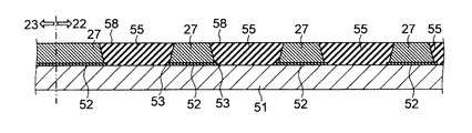
上述の図4〜図5Dに示す例においては、蒸着マスク20が、第1金属層32および第2金属層37という、少なくとも2つの金属層を積層させることによって構成される場合について説明した。しかしながら、これに限られることはなく、蒸着マスク20は、所定のパターンで複数の貫通孔25が形成された1つの金属層27によって構成されていてもよい。以下、図6A〜図7を参照して、蒸着マスク20が1つの金属層27を備える例について説明する。なお本変形例においては、蒸着マスク20の第1面20aから第2面20bに至る貫通孔25のうち第1面20a上に位置する部分を第1開口部30と称し、貫通孔25のうち第2面20b上に位置する部分を第2開口部35と称する。
In the example shown in FIGS. 4 to 5D described above, the case where the
はじめに、本変形例による蒸着マスク20を製造する方法について説明する。
First, a method for manufacturing the
まず、所定の導電性パターン52が形成された基材51を準備する。次に図6Aに示すように、基材51上に、所定の隙間56を空けてレジストパターン55を形成するレジスト形成工程を実施する。好ましくは、レジストパターン55の隙間56を画成するレジストパターン55の側面57の間の間隔は、基材51から遠ざかるにつれて狭くなっている。すなわち、レジストパターン55が、基材51から遠ざかるにつれてレジストパターン55の幅が広くなる形状、いわゆる逆テーパ形状を有している。
First, a
このようなレジストパターン55を形成する方法の一例について説明する。例えば、はじめに、基材51の面のうち導電性パターン52が形成された側の面上に、光硬化性樹脂を含むレジスト膜を設ける。次に、基材51のうちレジスト膜が設けられている側とは反対の側から基材51に入射させた露光光をレジスト膜に照射して、レジスト膜を露光する。その後、レジスト膜を現像する。この場合、露光光の回り込み(回折)に基づいて、図6Aに示すような逆テーパ形状を有するレジストパターン55を得ることができる。
An example of a method for forming such a resist
次に図6Bに示すように、レジストパターン55の隙間56にめっき液を供給して、導電性パターン52上に金属層27を析出させるめっき処理工程を実施する。その後、上述の除去工程および分離工程を実施することにより、図7に示すように、所定のパターンで貫通孔25が設けられた金属層27を備えた蒸着マスク20を得ることができる。金属層27の厚みは、例えば5〜50μmの範囲内になっている。
Next, as shown in FIG. 6B, a plating process is performed in which a plating solution is supplied to the
ところで上述のように、めっき処理工程においては、レジストパターン55の隙間56に供給されためっき液が、レジストパターン55と基材51との間に浸入してしまうことが生じ得る。浸入しためっき液がレジストパターン55と基材51との間で析出すると、貫通孔25の第1開口部30が形成されるべきであるが第1開口部30が形成されていない部分、すなわち不要部分が形成されることになる。このように本変形例においては、蒸着マスク20の第1面20a側に、レジストパターン55と基材51との間に浸入しためっき液に起因する不要部分が生じ得る。
As described above, in the plating process, the plating solution supplied to the
なお、図7に示す蒸着マスク20を作製するために用いられ得るレジストパターン55が、図6Aおよび図6Bに示すレジストパターン55に限られることはない。例えば、レジストパターン55が、基材51から遠ざかるにつれてレジストパターン55の幅が狭くなる形状、いわゆる順テーパ形状を有している場合であっても、図7に示す貫通孔25が設けられた蒸着マスク20を得ることができる。この場合、めっき処理工程によって形成される金属層27の面のうち基材51に接する側の面が、蒸着マスク20の第2面20bとなる。また、レジストパターン55の隙間56に供給されためっき液が、レジストパターン55と基材51との間に浸入する場合、不要部分が第2面20b側に形成されることになる。
Note that the resist
〔形態2 エッチングによって作製された蒸着マスク〕
上述の図4〜図7に示す例においては、めっき処理によって蒸着マスク20を作製する場合、および、この場合に生じ得る不要部分について説明した。しかしながら、蒸着マスク20を作製するために採用される方法が、めっき処理に限られることはない。以下、エッチングによって金属板21に貫通孔25を形成することによって蒸着マスク20を作製する例について説明する。
[Embodiment 2: Deposition mask produced by etching]
In the example shown in FIGS. 4 to 7 described above, the case where the
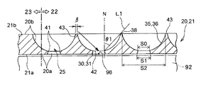
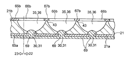
図8は、エッチングを利用することによって作製された蒸着マスク20を、図3のA−A線に沿って切断した場合を示す断面図である。図8に示す例では、後に詳述するように、蒸着マスクの法線方向における一方の側となる金属板21の第1面21aに第1開口部30がエッチングによって形成され、金属板21の法線方向における他方の側となる第2面21bに第2開口部35がエッチングによって形成される。第1開口部30は、第2開口部35に接続され、これによって第2開口部35と第1開口部30とが互いに通じ合うように形成される。貫通孔25は、第2開口部35と、第2開口部35に接続された第1開口部30とによって構成されている。
FIG. 8 is a cross-sectional view showing a case where the
図8に示すように、蒸着マスク20の第1面20aの側から第2面20bの側へ向けて、蒸着マスク20の法線方向に沿った各位置における蒸着マスク20の板面に沿った断面での各第1開口部30の断面積は、しだいに小さくなっていく。同様に、蒸着マスク20の法線方向に沿った各位置における蒸着マスク20の板面に沿った断面での各第2開口部35の断面積は、蒸着マスク20の第2面20bの側から第1面20aの側へ向けて、しだいに小さくなっていく。
As shown in FIG. 8, along the plate | board surface of the
図8に示すように、第1開口部30の壁面31と、第2開口部35の壁面36とは、周状の接続部41を介して接続されている。接続部41は、蒸着マスクの法線方向に対して傾斜した第1開口部30の壁面31と、蒸着マスクの法線方向に対して傾斜した第2開口部35の壁面36とが合流する張り出し部の稜線によって、画成されている。そして、接続部41は、蒸着マスク20の平面視において貫通孔25の面積が最小になる貫通部42を画成する。
As shown in FIG. 8, the
図8に示すように、蒸着マスクの法線方向に沿った一方の側の面、すなわち、蒸着マスク20の第1面20a上において、隣り合う二つの貫通孔25は、蒸着マスクの板面に沿って互いから離間している。すなわち、後述する製造方法のように、蒸着マスク20の第1面20aに対応するようになる金属板21の第1面21a側から当該金属板21をエッチングして第1開口部30を作製する場合、隣り合う二つの第1開口部30の間に金属板21の第1面21aが残存するようになる。
As shown in FIG. 8, on one surface along the normal direction of the vapor deposition mask, that is, on the
同様に、図8に示すように、蒸着マスクの法線方向に沿った他方の側、すなわち、蒸着マスク20の第2面20bの側においても、隣り合う二つの第2開口部35が、蒸着マスクの板面に沿って互いから離間していてもよい。すなわち、隣り合う二つの第2開口部35の間に金属板21の第2面21bが残存していてもよい。以下の説明において、金属板21の第2面21bの有効領域22のうちエッチングされずに残っている部分のことを、トップ部43とも称する。このようなトップ部43が残るように蒸着マスク20を作製することにより、蒸着マスク20に十分な強度を持たせることができる。このことにより、例えば搬送中などに蒸着マスク20が破損してしまうことを抑制することができる。なおトップ部43の幅βが大きすぎると、蒸着工程においてシャドーが発生し、これによって蒸着材料98の利用効率が低下することがある。従って、トップ部43の幅βが過剰に大きくならないように蒸着マスク20が作製されることが好ましい。例えば、トップ部43の幅βが2μm以下であることが好ましい。なおトップ部43の幅βは一般に、蒸着マスク20を切断する方向に応じて変化する。例えば、図8に示すトップ部43の幅βは互いに異なることがある。この場合、いずれの方向で蒸着マスク20を切断した場合にもトップ部43の幅βが2μm以下になるよう、蒸着マスク20が構成されていてもよい。
Similarly, as shown in FIG. 8, two adjacent
図8においても、上述の図4および図7に示す場合と同様に、蒸着マスク20の第2面20b側における貫通孔25(第2開口部35)の端部38を通る蒸着材料98の経路であって、有機EL基板92に到達することができる経路のうち、蒸着マスク20の法線方向Nに対してなす角度が最小となる経路が、符号L1で表されている。また、経路L1と蒸着マスク20の法線方向Nとがなす角度が、符号θ1で表されている。本形態においても、蒸着材料98の利用効率を高めるためには、角度θ1を大きくすることが好ましい。例えば、蒸着マスク20の強度を確保できる範囲内で可能な限り蒸着マスク20の厚みを小さくし、これによって角度θ1を大きくすることが好ましい。例えば蒸着マスク20の厚みは、80μm以下に、例えば10〜80μmの範囲内や20〜80μmの範囲内に設定される。蒸着の精度をさらに向上させるため、蒸着マスク20の厚みを、40μm以下に、例えば10〜40μmの範囲内や20〜40μmの範囲内に設定してもよい。なお蒸着マスク20の厚みは、周囲領域23の厚み、すなわち蒸着マスク20のうち第1開口部30および第2開口部35が形成されていない部分の厚みである。従って蒸着マスク20の厚みは、金属板21の厚みであると言うこともできる。
8, similarly to the case shown in FIGS. 4 and 7, the path of the
次に、図8に示す蒸着マスク20を、エッチングを利用して製造する方法について説明する。
Next, a method for manufacturing the
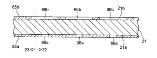
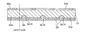
はじめに、所定の厚みを有する金属板21を準備する。金属板21を構成する材料としては、ニッケルを含む鉄合金などが用いられ得る。次に図9Aに示すように、金属板21の第1面21a上に、所定の隙間66aを空けて第1レジストパターン65aを形成する。また、金属板21の第2面21b上に、所定の隙間66bを空けて第2レジストパターン65bを形成する。
First, a
その後、図9Bに示すように、金属板21の第1面21aのうち第1レジストパターン65aによって覆われていない領域を、第1エッチング液を用いてエッチングする第1面エッチング工程を実施する。例えば、第1エッチング液が、金属板21の第1面21aに対面する側に配置されたノズルから、第1レジストパターン65a越しに金属板21の第1面21aに向けて噴射される。この結果、図9Bに示すように、金属板21の第1面21aのうち第1レジストパターン65aによって覆われていない領域で、第1エッチング液による浸食が進む。これによって、金属板21の第1面21aに多数の第1開口部30が形成される。第1エッチング液としては、例えば塩化第2鉄溶液および塩酸を含むものが用いられる。
Thereafter, as shown in FIG. 9B, a first surface etching process is performed in which the region of the
その後、図9Cに示すように、後の第2面エッチング工程において用いられる第2エッチング液に対する耐性を有した樹脂69によって、第1開口部30が被覆される。すなわち、第2エッチング液に対する耐性を有した樹脂69によって、第1開口部30が封止される。図9Cに示す例においては、樹脂69の膜が、形成された第1開口部30だけでなく、金属板21の第1面21a(第1レジストパターン65a)も覆うように形成されている。
Thereafter, as shown in FIG. 9C, the
次に、図9Dに示すように、金属板21の第2面21bのうち第2レジストパターン65bによって覆われていない領域をエッチングし、第2面21bに第2開口部35を形成する第2面エッチング工程を実施する。第2面エッチング工程は、第1開口部30と第2開口部35とが互いに通じ合い、これによって貫通孔25が形成されるようになるまで実施される。第2エッチング液としては、上述の第1エッチング液と同様に、例えば塩化第2鉄溶液および塩酸を含むものが用いられる。
Next, as shown in FIG. 9D, a region of the
なお第2エッチング液による浸食は、金属板21のうち第2エッチング液に触れている部分において行われていく。従って、浸食は、金属板21の法線方向(厚み方向)のみに進むのではなく、金属板21の板面に沿った方向にも進んでいく。ここで好ましくは、第2面エッチング工程は、第2レジストパターン65bの隣り合う二つの隙間66bに対面する位置にそれぞれ形成された二つの第2開口部35が、二つの隙間66bの間に位置するブリッジ部67bの裏側において合流するよりも前に終了される。これによって、図9Dに示すように、金属板21の第2面21bに上述のトップ部43を残すことができる。
Note that the erosion by the second etching solution is performed in the portion of the
その後、金属板21から樹脂69を除去する。これによって、金属板21に形成された複数の貫通孔25を備える蒸着マスク20を得ることができる。樹脂69は、例えばアルカリ系剥離液を用いることによって、除去することができる。アルカリ系剥離液が用いられる場合、樹脂69と同時にレジストパターン65a,65bも除去され得る。なお、樹脂69を除去した後、樹脂69を剥離させるための剥離液とは異なる剥離液を用いて、樹脂69とは別途にレジストパターン65a,65bを除去してもよい。
Thereafter, the
ところで、上述の第2面エッチング工程においては、エッチングを過剰に進行させてしまうと、金属板21の第2面21bに上述のトップ部43を残すことができなくなる。このため、トップ部43を確実に残すためには、エッチング時間を短めに設定することが好ましい。一方、トップ部43の幅βが大きすぎると、蒸着工程においてシャドーが発生し、これによって蒸着材料98の利用効率が低下してしまう。この場合、トップ部43のうちその幅βが設計値よりも大きくなっている部分は、第2開口部35が形成されるべきであるが第2開口部35が形成されずに金属板21の第2面21bが存在している部分、すなわち不要部分であると言える。また、エッチング速度やエッチング時間のばらつきなどによっても、蒸着マスク20のうち貫通孔25が形成されるべき部分に貫通孔25が正確に形成されずに、金属板21の第1面21a側や第2面21b側に不要部分が生じることも考えられる。このような課題を解決する方法については、後述する。
By the way, in the above-described second surface etching step, if the etching is excessively advanced, the above-described
変形例
上述の図8〜図9Dに示す例においては、金属板21を第1面21a側および第2面21b側の両方からエッチングすることによって蒸着マスク20が作製される例を示した。しかしながら、これに限られることはなく、図示はしないが、金属板21を第2面21b側からエッチングして、第2面21bから第1面21aへ至る貫通孔25を形成することにより、蒸着マスク20を作製してもよい。
Modifications In the example shown in FIGS. 8 to 9D described above, an example in which the
〔蒸着マスクの貫通孔の修正方法〕
以下、蒸着マスク20を作製する際に生じ得る上述の不要部分への対処方法について説明する。ここでは、上述のようにして蒸着マスク20を作製した後、不要部分にレーザー光を照射することによって貫通孔25の位置および形状を修正する例について、図10および図11(a)(b)を参照して説明する。
[Method of correcting through-holes in vapor deposition mask]
Hereinafter, a method for dealing with the above unnecessary portion that may occur when the
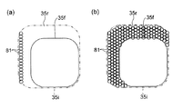
図10は、貫通孔25の第2開口部35が形成されるべきであるが第2開口部35が形成されていない不要部分35rが存在している蒸着マスク20を、第2面20b側から見た場合を示す平面図である。図10においては、蒸着マスク20の第2面20b上に形成されるべき、理想的な位置および形状を有する第2開口部(以下、理想第2開口部とも称する)が、符号35iが付された二点鎖線で表されている。また、理想第2開口部35iに比べて小さく形成された第2開口部(以下、不良第2開口部とも称する)に、符号35fが付されている。不要部分35rは、理想第2開口部35iと不良第2開口部35fとの間の部分として定義される。なお図10において、理想第2開口部35iとほぼ同一の形状を有しており、このためレーザー光による修正を施す必要がない第2開口部には符号35が付されている。なお図10や後述する図11(a)(b)においては、図が煩雑になることを防ぐため、蒸着マスク20を第2面20b側から見た場合に視認され得る第1開口部30の壁面31や接続部41の輪郭が省略されている。
In FIG. 10, the
なお図示はしないが、貫通孔25が形成されるべき部分に貫通孔25が全く形成されていないという事態も生じ得る。この場合、1つの貫通孔25に対応する部分全域が不要部分となる。
Although not shown, there may be a situation in which the through
(検出工程)
レーザー光を利用して貫通孔25を修正する方法においては、はじめに、蒸着マスク20のうち、貫通孔25の第2開口部35が形成されるべきであるが第2開口部35が形成されていない不要部分35rを検出する検出工程を実施する。例えば、はじめに、蒸着マスク20を第2面20b側から撮影装置で撮影して第2面画像を得る。次に、第2面画像に現れている第2開口部35の位置および形状と、理想第2開口部35iの位置および形状とを比較する。そして、理想第2開口部35iと不良第2開口部35fとの間に位置する部分であって、一定の幅または面積を超えている部分を、不要部分35rとして認定する。
(Detection process)
In the method of correcting the through-
なお第2面画像を利用した検査においては、蒸着マスク20や撮影装置に付着したゴミや、第2面画像における明暗のゆらぎなどに起因して、正常に第2開口部35が形成されている部分が誤って不要部分35rとして認定されてしまうことが生じ得る。このような検出ミスを防ぐため、第2面画像を利用した検査によって不要部分35rとして認定された部分を、拡大して撮影して確認したり、目視で確認したりしてもよい。
In the inspection using the second surface image, the
(除去工程)
次に、不要部分35rにレーザー光を照射して不要部分35rを除去する除去工程を実施する。これによって、所望の位置に所望の形状で形成された複数の貫通孔25を備える蒸着マスク20を得ることができる。
(Removal process)
Next, a removal step of removing the
図11(a)および図11(b)は、除去工程の一例を示す図である。図11(a)および図11(b)においては、金属板21の第2面21bに照射されたレーザー光のスポットが符号81で表されている。図11(a)および図11(b)に示すように、レーザー光は、スポット81のスポット径が、形成されるべき貫通孔25の寸法(ここでは理想第2開口部35iの寸法)よりも小さくなるよう、蒸着マスク20に照射される。例えば、第2面20bにおける理想第2開口部35iの開口寸法S2が15〜80μmの範囲内の場合、レーザー光のスポット81のスポット径は2〜70μmの範囲内に設定される。若しくは、レーザー光のスポット81が、理想第2開口部35iの輪郭に包含され得るよう、レーザー光が調整されてもよい。このようにレーザー光を設定することにより、レーザー光を照射することによって修正された後の第2開口部35の位置および形状を、理想第2開口部35iの位置および形状により精密に近づけることができる。また、蒸着マスク20の面のうちレーザー光が照射される側とは反対側の面(ここでは第1面20a)に、ばりが生じてしまうことを抑制することができる。特に、レーザー光が後述の平均出力を有し、かつ上述のスポット径を有する場合、高い出力のレーザー光が、細いスポット径に絞られた状態で蒸着マスク20に照射されるので、蒸着マスク20を切れ味良く打ち抜くことができ、第1面20aにばりが生じてしまうことを抑制することができる。
Fig.11 (a) and FIG.11 (b) are figures which show an example of a removal process. In FIG. 11A and FIG. 11B, the laser beam spot irradiated on the
除去工程においては、まず図11(a)に示すように、所定の第1方向に沿ってレーザー光を蒸着マスク20の第2面20b上で走査させる。その後、第1方向に交差する方向においてスポット81を移動させた後、所定の第1方向に沿ってレーザー光を蒸着マスク20の第2面20b上で走査させる。このような作業を繰り返すことにより、図11(b)に示すように、不要部分35rのほぼ全域にレーザー光を照射し、これによって不要部分35rを除去することができる。なお、レーザー光を走査させる方向が第1方向に限られることはなく、任意の方向において走査され得る。
In the removal step, first, as shown in FIG. 11A, laser light is scanned on the
不要部分35rを除去することができる限りにおいて、用いられるレーザー光のタイプ、波長や出力が特に限られることはない。一方、不要部分35rを効率的に除去するためには、蒸着マスク20を構成する材料によって吸収され易いレーザー光が用いられることが好ましい。例えば、蒸着マスク20を構成する材料のうち不要部分35rとなり得る部分が、ニッケルを含む鉄合金を有する場合、レーザー光が、YAGレーザー装置によって生成されるYAGレーザー光の第3高調波を含むことが好ましい。
As long as the
YAGレーザー装置としては、例えば、YAG(イットリウム・アルミニウム・ガーネット)にNd(ネオジム)を添加した結晶を発振用媒質として備えたものを用いることができる。この場合、基本波として、波長が約1064nmのレーザー光が生成される。また、基本波を非線形光学結晶に通すことによって、波長が約532nmの第2高調波が生成される。また、基本波および第2高調波を非線形光学結晶に通すことによって、波長が約355nmの第3高調波が生成される。 As the YAG laser device, for example, a YAG (yttrium, aluminum, garnet) added with Nd (neodymium) crystal as an oscillation medium can be used. In this case, laser light having a wavelength of about 1064 nm is generated as the fundamental wave. Further, by passing the fundamental wave through the nonlinear optical crystal, a second harmonic having a wavelength of about 532 nm is generated. Further, by passing the fundamental wave and the second harmonic through the nonlinear optical crystal, a third harmonic having a wavelength of about 355 nm is generated.
ところで、レーザー光が連続的に不要部分35rに照射される場合、レーザー光の照射に起因する熱が、不要部分35r以外の部分にまで伝わり、この結果、不要部分35rだけでなく不要部分35r以外の部分も除去されてしまうことが考えられる。また、吸収した熱に起因して不要部分35rが飛散する際のエネルギーが大きくなり、この結果、不要部分35rが広域にわたって飛散し、これによって、蒸着マスク20の表面が汚染されてしまうことも考えられる。このような課題を考慮すると、好ましくは、除去工程においては、レーザー光のパルスが間欠的に不要部分35rに照射される。言い換えると、不要部分35rに照射されるレーザー光として、連続光ではなく、パルス発振によって得られるパルスを含むレーザー光が用いられることが好ましい。これによって、レーザー光の照射に起因する熱が不要部分35r以外の部分にまで伝わることを抑制することができる。また、不要部分35rが広域にわたって飛散することを抑制することができる。
By the way, when the laser beam is continuously irradiated to the
レーザー光のパルスの平均出力およびパルスの幅は、レーザー光の照射に起因する熱が不要部分35r以外の部分にまで伝わることを抑制し、かつ、不要部分35rが広域にわたって飛散することを抑制するように設定されることが好ましい。例えば、レーザー光のパルスの平均出力は、1.5〜2.0mJの範囲内に設定され、レーザー光のパルスの幅は、5〜7nsの範囲内に設定される。一方、レーザー光のパルスの平均出力や幅が小さくなり過ぎると、不要部分35rを除去することに要する時間が長くなってしまう。この点を考慮すると、レーザー光のパルスの繰り返し周期は短い方が好ましい。例えばレーザー光のパルスの繰り返し周期は、1〜60nsの範囲内に設定される。
The average output and the pulse width of the pulse of the laser light suppress the heat caused by the laser light irradiation from being transmitted to a part other than the
本実施の形態によれば、第2開口部35が形成されるべきであるが第2開口部35が形成されていない不要部分35rが蒸着マスク20の第2面20b上に存在している場合であっても、不要部分35rにレーザー光を照射することにより、不要部分35rを除去することができる。このようにして蒸着マスク20の貫通孔25の位置や形状を修正することにより、その後の検査工程において蒸着マスク20が不良品と判定されてしまうことを抑制することができる。このことにより、蒸着マスク20の製造の歩留りを向上させることができる。
According to the present embodiment, when the
なお上述の本実施の形態においては、蒸着マスク20の貫通孔25のうち第2面20b上における貫通孔25(すなわち第2開口部35)の位置や形状を、レーザーを利用して修正する例を示したが、これに限られることはない。例えば、蒸着マスク20の第1面20a上における貫通孔25(すなわち第1開口部30)の位置や形状も、理想的な位置および形状を有する第1開口部からずれることがあり、このため第1面20a上に不要部分が存在することがあると考えられる。また、蒸着マスク20の第1面20aと第2面20bとの間において、第1開口部30の壁面31や第2開口部35の壁面36にも、貫通孔25が形成されるべきであるが貫通孔25が形成されていない部分、すなわち不要部分が存在することがあると考えられる。上述の除去工程においては、このような不要部分にレーザー光を照射して不要部分を除去してもよい。例えば、蒸着マスク20に対するレーザー光の入射角度を調整することにより、蒸着マスク20の第2面20b側から、第1面20a上の不要部分や第1面20aと第2面20bとの間の不要部分にレーザー光を照射することが可能である。
In the above-described embodiment, the position and shape of the through hole 25 (that is, the second opening 35) on the
また上述の本実施の形態の除去工程においては、蒸着マスク20の第2面20b側から不要部分にレーザー光を照射する例を示したが、これに限られることはなく、蒸着マスク20の第1面20a側から不要部分にレーザー光を照射してもよい。例えば、蒸着マスク20の第1面20a側から、第1面20a上の不要部分、第2面20b上の不要部分35rや第1面20aと第2面20bとの間の不要部分にレーザー光を照射してもよい。
Moreover, in the removal process of this Embodiment mentioned above, although the example which irradiates a laser beam to an unnecessary part from the
なお、蒸着マスク20の第1面20a側から蒸着マスク20に向けてレーザー光を照射した場合、レーザー光によって除去された不要部分は、主に蒸着マスク20の第1面20a側で飛散すると考えられる。このため、蒸着マスク20の第1面20a側から蒸着マスク20に向けてレーザー光を照射する場合は、蒸着マスク20の第2面20b側から蒸着マスク20に向けてレーザー光を照射する場合に比べて、飛散した除去部分が蒸着マスク20の第1面20aに付着し易くなる。一方、蒸着マスク20の第1面20aは、蒸着マスク20を利用して蒸着材料を有機EL基板92に蒸着させる蒸着工程の際に、有機EL基板92に密着する面である。従って、蒸着マスク20の第1面20aに不要部分が多く付着していると、蒸着工程の間にそのような不要部分が蒸着マスク20の第1面20aから有機EL基板92に転移して、有機EL基板92が汚染されてしまうことが考えられる。このような課題を考慮すると、除去工程の際に蒸着マスク20の第1面20aが汚染されてしまうことを抑制するために、蒸着マスク20の第2面20b側から蒸着マスク20に向けてレーザー光を照射することが好ましいと言える。
In addition, when a laser beam is irradiated from the
なお、上述した実施の形態に対するいくつかの変形例を説明してきたが、当然に、複数の変形例を適宜組み合わせて適用することも可能である。 In addition, although some modified examples with respect to the above-described embodiment have been described, naturally, a plurality of modified examples can be applied in combination as appropriate.
20 蒸着マスク
20a 第1面
20b 第2面
21 金属板
22 有効領域
23 周囲領域
25 貫通孔
30 第1開口部
31 壁面
32 第1金属層
35 第2開口部
35f 不良第2開口部
35i 理想第2開口部
35r 不要部分
36 壁面
37 第2金属層
41 接続部
43 トップ部
51 基材
52 導電性パターン
55 レジストパターン
56 隙間
65a 第1レジストパターン
65b 第2レジストパターン
81 スポット
92 有機EL基板
98 蒸着材料
DESCRIPTION OF
Claims (6)
複数の貫通孔が形成された蒸着マスクを準備する準備工程と、
前記蒸着マスクのうち、前記貫通孔が形成されるべきであるが前記貫通孔が形成されていない不要部分を検出する検出工程と、
前記不要部分にレーザー光を照射して前記不要部分を除去する除去工程と、を備え、
除去工程において前記不要部分に照射される前記レーザー光のスポット径は、形成されるべき貫通孔の寸法よりも小さい、蒸着マスク製造方法。 A vapor deposition mask manufacturing method comprising:
A preparation step of preparing a vapor deposition mask in which a plurality of through holes are formed;
Of the vapor deposition mask, the detection step of detecting the unnecessary portion where the through hole is to be formed but the through hole is not formed,
Removing the unnecessary portion by irradiating the unnecessary portion with laser light, and
The vapor deposition mask manufacturing method, wherein a spot diameter of the laser light applied to the unnecessary portion in the removing step is smaller than a dimension of the through hole to be formed.
前記レーザー光は、YAGレーザー装置によって生成されるYAGレーザー光の第3高調波を含む、請求項1に記載の蒸着マスク製造方法。 The unnecessary portion has an iron alloy containing nickel,
The said laser beam is a vapor deposition mask manufacturing method of Claim 1 containing the 3rd harmonic of the YAG laser beam produced | generated by a YAG laser apparatus.
前記第2面における前記貫通孔の開口寸法は、前記第1面における前記貫通孔の開口寸法よりも大きく、
前記レーザー光は、前記第2面側から前記不要部分に照射される、請求項1または2に記載の蒸着マスク製造方法。 The deposition mask includes a first surface facing the substrate when a deposition material is deposited on the substrate using the deposition mask, and a second surface located on the opposite side of the first surface,
The opening size of the through hole in the second surface is larger than the opening size of the through hole in the first surface,
The vapor deposition mask manufacturing method according to claim 1, wherein the unnecessary portion is irradiated with the laser light from the second surface side.
前記レーザー光の前記パルスの平均出力は、1.5〜2.0mJの範囲内であり、
前記レーザー光の前記パルスの幅は、5〜7nsの範囲内であり、
前記レーザー光の前記パルスの周期は、1〜60nsの範囲内である、請求項1乃至3のいずれか一項に記載の蒸着マスク製造方法。 In the removing step, the unnecessary part is intermittently irradiated with the pulse of the laser beam,
The average output of the pulses of the laser light is in the range of 1.5 to 2.0 mJ,
The width of the pulse of the laser light is in the range of 5 to 7 ns,
The vapor deposition mask manufacturing method according to any one of claims 1 to 3, wherein a period of the pulse of the laser light is in a range of 1 to 60 ns.
所定の基材上に、所定の隙間を空けてレジストパターンを形成するレジスト形成工程と、
前記レジストパターンの前記隙間において金属層を析出させるめっき処理工程と、
前記金属層を前記基材から分離させる分離工程と、を有する、請求項1乃至4のいずれか一項に記載の蒸着マスク製造方法。 The preparation step includes
A resist forming step of forming a resist pattern on a predetermined substrate with a predetermined gap;
A plating process for depositing a metal layer in the gap of the resist pattern;
The vapor deposition mask manufacturing method as described in any one of Claims 1 thru | or 4 which has the isolation | separation process which isolate | separates the said metal layer from the said base material.
金属板を準備する工程と、
前記金属板上に、所定の隙間を空けてレジストパターンを形成するレジスト形成工程と、
前記金属板のうち前記レジストパターンによって覆われていない領域をエッチングして、前記金属板に前記貫通孔を形成する工程と、を有する、請求項1乃至4のいずれか一項に記載の蒸着マスク製造方法。 The preparation step includes
Preparing a metal plate;
On the metal plate, a resist forming step of forming a resist pattern with a predetermined gap,
Etching a region of the metal plate that is not covered with the resist pattern to form the through hole in the metal plate, the vapor deposition mask according to any one of claims 1 to 4. Production method.
Priority Applications (1)
| Application Number | Priority Date | Filing Date | Title |
|---|---|---|---|
| JP2015076129A JP6536941B2 (en) | 2015-04-02 | 2015-04-02 | Deposition mask manufacturing method |
Applications Claiming Priority (1)
| Application Number | Priority Date | Filing Date | Title |
|---|---|---|---|
| JP2015076129A JP6536941B2 (en) | 2015-04-02 | 2015-04-02 | Deposition mask manufacturing method |
Publications (2)
| Publication Number | Publication Date |
|---|---|
| JP2016196675A true JP2016196675A (en) | 2016-11-24 |
| JP6536941B2 JP6536941B2 (en) | 2019-07-03 |
Family
ID=57357539
Family Applications (1)
| Application Number | Title | Priority Date | Filing Date |
|---|---|---|---|
| JP2015076129A Active JP6536941B2 (en) | 2015-04-02 | 2015-04-02 | Deposition mask manufacturing method |
Country Status (1)
| Country | Link |
|---|---|
| JP (1) | JP6536941B2 (en) |
Cited By (4)
| Publication number | Priority date | Publication date | Assignee | Title |
|---|---|---|---|---|
| WO2019054462A1 (en) * | 2017-09-15 | 2019-03-21 | 凸版印刷株式会社 | Method for manufacturing deposition mask, method for manufacturing display device and deposition mask |
| JP2019072763A (en) * | 2017-10-11 | 2019-05-16 | エーピー システムズ インコーポレイテッド | Laser processing method |
| CN110066975A (en) * | 2019-05-14 | 2019-07-30 | 京东方科技集团股份有限公司 | The design method of opening is deposited in mask plate, evaporation coating device, evaporation coating method and mask plate |
| DE112017007305B4 (en) | 2017-03-24 | 2022-12-15 | Mitsubishi Electric Corporation | Method of manufacturing a semiconductor device and semiconductor device |
Citations (2)
| Publication number | Priority date | Publication date | Assignee | Title |
|---|---|---|---|---|
| JP2005154879A (en) * | 2003-11-28 | 2005-06-16 | Canon Components Inc | Metal mask for vapor deposition, and method of producing vapor deposition pattern using the same |
| JP2009068082A (en) * | 2007-09-14 | 2009-04-02 | Sony Corp | Method for manufacturing vapor-deposition mask, and vapor-deposition mask |
-
2015
- 2015-04-02 JP JP2015076129A patent/JP6536941B2/en active Active
Patent Citations (2)
| Publication number | Priority date | Publication date | Assignee | Title |
|---|---|---|---|---|
| JP2005154879A (en) * | 2003-11-28 | 2005-06-16 | Canon Components Inc | Metal mask for vapor deposition, and method of producing vapor deposition pattern using the same |
| JP2009068082A (en) * | 2007-09-14 | 2009-04-02 | Sony Corp | Method for manufacturing vapor-deposition mask, and vapor-deposition mask |
Cited By (10)
| Publication number | Priority date | Publication date | Assignee | Title |
|---|---|---|---|---|
| DE112017007305B4 (en) | 2017-03-24 | 2022-12-15 | Mitsubishi Electric Corporation | Method of manufacturing a semiconductor device and semiconductor device |
| WO2019054462A1 (en) * | 2017-09-15 | 2019-03-21 | 凸版印刷株式会社 | Method for manufacturing deposition mask, method for manufacturing display device and deposition mask |
| JPWO2019054462A1 (en) * | 2017-09-15 | 2019-11-07 | 凸版印刷株式会社 | Vapor deposition mask manufacturing method and display device manufacturing method |
| CN111032902A (en) * | 2017-09-15 | 2020-04-17 | 凸版印刷株式会社 | Method for manufacturing vapor deposition mask, method for manufacturing display device, and vapor deposition mask |
| JP2020109214A (en) * | 2017-09-15 | 2020-07-16 | 凸版印刷株式会社 | Vapor deposition mask |
| CN111032902B (en) * | 2017-09-15 | 2021-03-02 | 凸版印刷株式会社 | Method for manufacturing vapor deposition mask, method for manufacturing display device, and vapor deposition mask |
| JP7222376B2 (en) | 2017-09-15 | 2023-02-15 | 凸版印刷株式会社 | Evaporation mask manufacturing method |
| JP2019072763A (en) * | 2017-10-11 | 2019-05-16 | エーピー システムズ インコーポレイテッド | Laser processing method |
| JP7246884B2 (en) | 2017-10-11 | 2023-03-28 | エーピーエス ホールディングス コーポレイション | Laser processing method |
| CN110066975A (en) * | 2019-05-14 | 2019-07-30 | 京东方科技集团股份有限公司 | The design method of opening is deposited in mask plate, evaporation coating device, evaporation coating method and mask plate |
Also Published As
| Publication number | Publication date |
|---|---|
| JP6536941B2 (en) | 2019-07-03 |
Similar Documents
| Publication | Publication Date | Title |
|---|---|---|
| KR102471409B1 (en) | Deposition mask device and method for manufacturing the deposition mask device | |
| US11211558B2 (en) | Deposition mask device and method of manufacturing deposition mask device | |
| TWI614354B (en) | Deposition mask | |
| US11380546B2 (en) | Deposition mask, deposition mask apparatus, manufacturing method of deposition mask, and manufacturing method of deposition mask apparatus | |
| JP5515025B2 (en) | Mask, mask member used therein, mask manufacturing method, and organic EL display substrate manufacturing method | |
| JP2013245392A (en) | Vapor deposition mask and method for manufacturing the same | |
| JP2016148112A (en) | Method of manufacturing vapor deposition mask, and vapor deposition mask | |
| CN213232465U (en) | Vapor deposition mask, vapor deposition mask device, and intermediate body | |
| JP6536941B2 (en) | Deposition mask manufacturing method | |
| JP6240960B2 (en) | Method for manufacturing film formation mask and film formation mask | |
| JP6078746B2 (en) | Manufacturing method of vapor deposition mask | |
| US20210193928A1 (en) | Manufacturing method of deposition mask and manufacturing method of organic el display | |
| JP2020026553A (en) | Vapor deposition mask, and vapor deposition mask manufacturing method | |
| JP6701543B2 (en) | Vapor deposition mask and method for manufacturing vapor deposition mask | |
| JP2017141500A (en) | Vapor deposition mask, and production of vapor deposition mask | |
| CN111485194A (en) | Vapor deposition mask, vapor deposition mask device, method for manufacturing vapor deposition mask device, intermediate, vapor deposition method, and method for manufacturing organic E L display device | |
| JP2017186617A (en) | Vapor deposition mask, and production method of vapor deposition mask | |
| JP6372755B2 (en) | Method for manufacturing vapor deposition mask, metal plate used for producing vapor deposition mask, and vapor deposition mask | |
| JP7047828B2 (en) | Vapor deposition mask and manufacturing method of vapor deposition mask | |
| JP2017101302A (en) | Vapor deposition mask, and production method of vapor deposition mask | |
| JP2017206732A (en) | Vapor deposition mask welding method | |
| JP2018095897A (en) | Vapor deposition mask, and washing method of vapor deposition mask | |
| JP2018202449A (en) | Laser processing method | |
| JP2019196533A (en) | Vapor deposition mask, washing method of vapor deposition mask, and vapor deposition method | |
| JP2017160470A (en) | Manufacturing method of vapor deposition mask device and vapor deposition mask device |
Legal Events
| Date | Code | Title | Description |
|---|---|---|---|
| A621 | Written request for application examination |
Free format text: JAPANESE INTERMEDIATE CODE: A621 Effective date: 20180226 |
|
| A977 | Report on retrieval |
Free format text: JAPANESE INTERMEDIATE CODE: A971007 Effective date: 20180921 |
|
| A131 | Notification of reasons for refusal |
Free format text: JAPANESE INTERMEDIATE CODE: A131 Effective date: 20181026 |
|
| A521 | Request for written amendment filed |
Free format text: JAPANESE INTERMEDIATE CODE: A523 Effective date: 20181218 |
|
| TRDD | Decision of grant or rejection written | ||
| A01 | Written decision to grant a patent or to grant a registration (utility model) |
Free format text: JAPANESE INTERMEDIATE CODE: A01 Effective date: 20190510 |
|
| A61 | First payment of annual fees (during grant procedure) |
Free format text: JAPANESE INTERMEDIATE CODE: A61 Effective date: 20190523 |
|
| R150 | Certificate of patent or registration of utility model |
Ref document number: 6536941 Country of ref document: JP Free format text: JAPANESE INTERMEDIATE CODE: R150 |