JP2016167929A - Power supply controller - Google Patents
Power supply controller Download PDFInfo
- Publication number
- JP2016167929A JP2016167929A JP2015046957A JP2015046957A JP2016167929A JP 2016167929 A JP2016167929 A JP 2016167929A JP 2015046957 A JP2015046957 A JP 2015046957A JP 2015046957 A JP2015046957 A JP 2015046957A JP 2016167929 A JP2016167929 A JP 2016167929A
- Authority
- JP
- Japan
- Prior art keywords
- circuit
- power supply
- state
- discharge
- switch circuit
- Prior art date
- Legal status (The legal status is an assumption and is not a legal conclusion. Google has not performed a legal analysis and makes no representation as to the accuracy of the status listed.)
- Pending
Links
Images


Abstract
Description
本発明は、電源制御装置に関するものである。 The present invention relates to a power supply control device.
インバータを介して直流対応型ブラシレスモータに電源を接続するための電源回路を備えて電動機用駆動装置が開示されている。この電動機用駆動装置では、電源回路に対して、互いに並列接続された平滑用コンデンサ及び放電用抵抗から成る放電回路が接続されている。また放電用抵抗には電流を通電又は遮断するためのノーマルクローズ型リレーRY3が直列接続されている。ノーマルクローズ型リレーRY3はコントローラの制御により電源回路がオン状態になったときに開放状態となって放電用抵抗に流れる電流を遮断し、オフ状態になったときのみ閉状態となって放電用抵抗に流れる電流を通電させて平滑用コンデンサに充電させる(特許文献1)。 An electric motor drive device having a power supply circuit for connecting a power supply to a DC-compatible brushless motor via an inverter is disclosed. In this electric motor drive device, a discharge circuit including a smoothing capacitor and a discharge resistor connected in parallel to each other is connected to a power supply circuit. Also the discharge resistor is normally closed relay RY 3 for energizing or interrupting the current are connected in series. Normally closed relay RY 3 cuts off the current flowing through the discharge resistor in an open state when the power circuit is turned on by the control of the controller, for discharging a look closed state when turned off A current flowing through the resistor is energized to charge the smoothing capacitor (Patent Document 1).
しかしながら、上記の電動機用駆動装置では、電源回路のオン、オフの切替と、ノーマルクローズ型リレーRY3の切替を、コントローラから制御信号を送信するだけで行っている。そのため、例えば、電源回路のオン、オフの切替、及び、ノーマルクローズ型リレーRY3の切替を高速に行った場合には、電源回路のオン時間と、ノーマルクローズ型リレーRY3の閉状態の時間が重なり、電源と放電回路との間が短絡するという問題があった。 However, in the above motor drive device, on the power supply circuit, and switching off the switch of normally-closed relay RY 3, it is performed simply by transmitting a control signal from the controller. Therefore, for example, on the power circuit, switching off, and, when performing switching of the normally-closed relay RY 3 at high speed, and on-time of the power supply circuit, the time of closing of normally-closed relay RY 3 And the power supply and the discharge circuit are short-circuited.
本発明が解決しようとする課題は、電源と放電回路との間の短絡を防ぐ電源制御装置を提供することである。 The problem to be solved by the present invention is to provide a power supply control device that prevents a short circuit between a power supply and a discharge circuit.
本発明は、一対の電源ラインの間に接続されたコンデンサと、電源の正極から負荷を介して電源の負極までの電流経路に接続され、前記電流経路の導通及び遮断を切り替えるスイッチ回路と、電源ラインに接続され、コンデンサを放電させる放電回路と、スイッチ回路及び放電回路の一方の回路である第1回路と、スイッチ回路及びスイッチ回路の他方の回路である第2回路とを連動させる連動手段とを備え、連動手段により、第1回路の導通状態から放電状態への切り替わりに対して、第2回路を遮断状態から導通状態への切り替わりを連動させることによって上記課題を解決する。 The present invention includes a capacitor connected between a pair of power supply lines, a switch circuit connected to a current path from the positive electrode of the power supply to the negative electrode of the power supply via a load, and switching between conduction and interruption of the current path; A discharge circuit that is connected to the line and discharges the capacitor; a first circuit that is one of the switch circuit and the discharge circuit; and an interlocking means that links the second circuit that is the other circuit of the switch circuit and the switch circuit; The above-mentioned problem is solved by interlocking the switching of the second circuit from the cutoff state to the conducting state with respect to the switching of the first circuit from the conducting state to the discharging state by the interlocking means.
本発明は、第1回路の導通状態から放電状態への切り替わりに連動して、第2回路が遮断状態から導通状態に切り替わるため、第1回路と第2回路が共に導通状態にならず、電源からスイッチ回路を介して放電回路までの電流経路が短絡することを防止できる。 In the present invention, since the second circuit is switched from the cutoff state to the conductive state in conjunction with the switching of the first circuit from the conductive state to the discharge state, both the first circuit and the second circuit are not in the conductive state. Can be prevented from short-circuiting the current path to the discharge circuit through the switch circuit.
以下、本発明の実施形態を図面に基づいて説明する。
《第1実施形態》
Hereinafter, embodiments of the present invention will be described with reference to the drawings.
<< First Embodiment >>
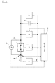
図1は、本実施形態に係る電源制御装置のブロック図である。本実施形態に係る電源制御装置は、例えば車両に設けられており、車両に搭載されたバッテリの電力を、インバータを介してモータに供給するシステムを制御する装置である。以下の説明では、電源制御装置が車両に設けられる場合を前提に説明するが、電源制御装置は車両に限らず他の装置に設けられていてもよい。例えば、電源制御装置は、定置用の電源の電力を負荷に供給する際の電力システムに適用されてもよい。 FIG. 1 is a block diagram of a power supply control device according to the present embodiment. The power supply control device according to the present embodiment is a device that is provided in a vehicle, for example, and controls a system that supplies electric power of a battery mounted on the vehicle to a motor via an inverter. The following description will be made on the assumption that the power supply control device is provided in the vehicle, but the power supply control device is not limited to the vehicle and may be provided in another device. For example, the power supply control device may be applied to a power system that supplies power from a stationary power supply to a load.
図1に示すように、電源制御装置は、電源1と、電力変換器2と、スイッチ回路3と、信号発生器4と、コンデンサ5と、放電回路6と、電圧センサ7と、コントローラ10と、電源ラインP、Nを備えている。
As shown in FIG. 1, the power supply control device includes a
主電源1は、電力変換器2に対して電力を供給するためのバッテリである。電源1は、リチウムイオン電池等の二次電池を複数接続している。主電源1の正極は、電源ラインPを介して電力変換器2に接続されており、主電源1の負極は電源ラインNを介して電力変換器2に接続されている。なお、主電源1には、直流電源に限らず、系統などの交流電源であってもよい。本実施形態のように、主電源1が二次電池により構成される場合には、電源1は、モータ(図示しない)の回生により電力を蓄電することもできる。モータは、電力変換器2の出力側(AC側)に接続される。また、主電源1が系統の場合には、主電源1は、電源1から電力変換器(ACDCコンバータなど)への電力供給や、電力変換器からの余剰電力の受給も可能である。また、主電源1は、交流又は直流を選択して出力することも可能である。このとき、出力される交流波形は、正弦波に限らず任意の波形でもよい。
The
電力変換器2は、主電源1の電力を変換し、モータ等の負荷に出力するインバータ又はコンバータである。電力変換器2には、IGBT等の複数のスイッチング素子がブリッジ状に接続されている。電力変換器2の出力側にモータを接続し、モータが回生した場合には、電力変換器2は電力の供給源としても機能する。
The
電源ラインP、Nは、主電源1と電力変換器2との間を接続する一対の配線である。また、電源ラインP、Nは、主電源1の正極から電力変換器2を介して主電源1の負極までの電流経路となる。
The power supply lines P and N are a pair of wirings that connect between the
スイッチ回路3は、信号発生器4からの信号によりオン(短絡)及びオフ(開放)を切り替える。スイッチ回路3は、機械式リレー又は半導体スイッチ等により構成されている。機械式リレーは、例えば接点及びコイルを有している。コイルに対して電流を流すと、電磁誘導により接点が移動する構造になっている。半導体スイッチは、MOSFET等のトランジスタである。スイッチ回路3は、駆動電源(図示しない)から供給される制御電圧又は制御電流によって、電流経路の電流量を変更可能なスイッチである。スイッチ回路3がオン状態のときには、主電源1と電力変換器2とを接続する電流経路が導通状態となり、スイッチ回路3がオフ状態のときには、当該電流経路が遮断状態となる。スイッチ回路3は、主電源1と電力変換器2との間で、電源ラインPに接続されている。
The
スイッチ回路3は、ノーマリオフのスイッチである。すなわち、スイッチ回路3は、主電源1から負荷に対して電力の要求がない場合には、オフ状態を維持している。これにより、スイッチ回路3のオン、オフを切り替える制御信号が、停電等により途絶えた場合でも、電流経路は遮断された状態で維持され、主電源1から電力変換器2へ電力が供給されることはないため、システムの安全性を高めることができる。
The
信号発生器4は、スイッチ回路3のオフ、オフを切り替えるための信号を発生し、スイッチ回路3に出力する。信号発生器4はコントローラ10により制御されている。
The
コンデンサ5は、電力変換器2の入力側に接続されている。またコンデンサ5は電源ラインPと電源ラインNとの間に接続されている。コンデンサ5は、リップル電流の平滑、或いは、ノイズフィルタとして機能する。
The
放電回路6は、コンデンサ5に充電された電荷を放電するための回路である。放電回路6は、電源ラインPと電源ラインNとの間に接続されている。放電回路6は、配線を介してコンデンサ5に接続されている。また放電回路6は、電源ラインP、Nに接続されており、スイッチ回路3を介して、主電源1に電気的に接続されている。放電回路6は、例えば、放電用の抵抗とスイッチとを接続した回路、又は、コイルと抵抗とを接続した回路等である。放電回路6に含まれるスイッチは、半導体スイッチ又はリレーである。放電回路6は、コンデンサ5と電気的に導通した状態(導通状態)と、コンデンサ5と電気的に遮断された状態(遮断状態)とを切り替える回路でもある。放電回路6が導通状態の場合には、コンデンサ5が放電され、コンデンサ5から放電回路6に電流が流れ、放電回路6で消費される。また、放電回路6が遮断状態の場合には、コンデンサ5は放電されず、コンデンサ5と放電回路6との間で閉回路が形成されない状態となる。放電回路6は、コントローラ10の制御信号に基づいて、コンデンサ5を放電させる。
The
電圧センサ7は、スイッチ回路3に対して並列に接続されており、スイッチ回路3の両端の電圧を検出する。電圧センサ7の検出電圧はコントローラ10に出力される。
The
コントローラ10は、スイッチ回路3と放電回路6とを連動させるように、スイッチ回路3及び放電回路6を制御する制御装置である。コントローラ10は、スイッチ回路3の導通状態から遮断状態の切り替わりに対して、放電回路6の遮断状態から導通状態への切り替わりを連動させる。また、コントローラ10は、スイッチ回路3の遮断状態から導通状態の切り替わりに対して、放電回路6の導通状態から遮断状態への切り替わりを連動させる。コントローラ10は、電圧センサ7を用いて、スイッチ回路3の導通状態及び遮断状態を検出する。そして、コントローラ10は、スイッチ回路3の導通状態から遮断状態への切り替わりを検出した場合には、放電回路6を遮断状態から導通状態に切り替える。また、コントローラ10は、スイッチ回路3の遮断状態から導通状態への切り替わりを検出した場合には、放電回路6を導通状態から遮断状態に切り替える。すなわち、コントローラ10は、センサ7を用いて、スイッチ回路3の状態(導通状態、遮断状態)を判断しつつ、その判断結果に基づいて放電回路6の状態を切り替えることで、スイッチ回路3と放電回路6とを連動させている。
The
次に、図2を用いて、スイッチ回路3と放電回路6の動作を説明する。図2は、信号発生器4から出力される信号の特性、スイッチ回路3の状態、及び、放電回路6の状態を説明するためのグラフである。信号発生器4の出力信号は、ローレベルで接続指示を示し、ハイレベルで開放指示を示している。接続指示は、スイッチ回路3を導通状態にするための指示である。開放指示は、スイッチ回路3を開放状態にするための指示である。スイッチ回路3の状態は、主電源1からスイッチ回路3に入力される電位と、スイッチ回路3から電力変換器2へ出力される電位との電位差で表されており、電圧センサ7の検出電圧に相当する。そして、図2で示した、スイッチ回路3のグラフの縦軸の表示について、「接続」は、スイッチ回路3の導通状態であることを示し、「開放」はスイッチ回路3の遮断状態を示す。放電回路6の状態は、放電回路の入力と出力との間の電位差で表されている。図3で示した、放電回路6のグラフの縦軸の表示について、「非放電」は、放電回路6の遮断状態であることを示し、「放電」は放電回路6の導通状態を示す。
Next, the operation of the
初期状態として、スイッチ回路3は導通状態であり、主電源1は電力変換器2に対して電力を供給しており、コンデンサ5はチャージされた状態である。また、放電回路6は遮断状態である。
As an initial state, the
まず、コントローラ10は、信号発生器4から開放指示を示す信号を出力するように、信号発生器4に対して制御信号を出力する。信号発生器4は、時間t1で、信号発生器4の信号レベルを立ち上げる。出力信号のレベルは、所定の時間遅れをもって、立ち上がり、時間t2でハイレベルになる。スイッチ回路3は、開放指示を示す出力信号をトリガとして、導通状態から遮断状態に切り替わる。このとき、電力変換器7などで、主電源1の電力を消費している場合に、スイッチ回路3の開放動作に伴い、電流経路の抵抗は高くなり、電流は低下する。そして、スイッチ回路3の入出力間の電位差が高くなる。そのため、図2に示すように、電圧センサ7の検出電圧は、時間t2から立ち上がる。
First, the
コントローラ10には、スイッチ回路3の状態を判断するための閾値が予め設定されている。閾値(Vth)は、スイッチ回路3が導通状態から遮断状態に切り替わったことを示す値であって、スイッチ回路3の入力間の電位差に対応した電圧値で表される。そして、コントローラ10は、センサ7の検出電圧が閾値より高くなった場合に、スイッチ回路3が導通状態から遮断状態に切り替わったと検出する。図2の例では、コントローラ10は、時間t3で、スイッチ回路3が導通状態から遮断状態に切り替わったと検出する。
The
コントローラ10は、時間t3で、スイッチ回路3が導通状態から遮断状態に切り替わったことを検出すると、放電回路6を遮断状態から導通状態に切り替える。これにより、コントローラ10は、スイッチ回路3の導通状態から遮断状態への切り替わりに対して、放電回路6の遮断状態から導通状態への切り替わりを連動させている。
The
スイッチ回路3が遮断状態から導通状態に切り替わる際には、まず、信号発生器4からの出力信号がハイレベルからローレベルに下がると、スイッチ回路3は遮断状態から導通状態に切り替わる動作を行う。そして、スイッチ回路3の動作に伴い、スイッチ回路3の入出力間の電位差が下がる。コントローラ10は、電圧センサ7の検出電圧が閾値より低くなると、スイッチ回路3が遮断状態から導通状態に切り替わったことを、検出する。そして、コントローラ10は、放電回路6を導通状態から遮断状態に切り替える、これにより、コントローラ10は、スイッチ回路3の遮断状態から導通状態の切り替わりに対して、放電回路6の導通状態から遮断状態への切り替わりを連動させている。
When the
上記のように、本実施形態は、スイッチ回路3の導通状態から遮断状態への切り替わりに対して、放電回路6の遮断状態から導通状態への切り替わりを連動させている。これにより、主電源1からスイッチ回路3を介して放電回路6までの電流経路が短絡すること(以下、電源短絡とも称す)を防止できる。その結果として、放電回路の保護を図ることができ、高い冗長性を保つことができる。主電源1と電力変換器2の間が導通している状態で、緊急時に電力変換器2の入力側の電荷を放電したい場合には、放電回路6を高速で導通状態にしなければならない。このような場合でも、本実施形態では、スイッチ回路3と放電回路6が共に導通状態にならないため、電源短絡を防止できる。
As described above, in the present embodiment, the switching of the
また本実施形態は、スイッチ回路3の遮断状態から導通状態への切り替わりに対して、放電回路6の導通状態から遮断状態への切り替わりを連動させている。これにより、電源短絡を防止できる。
In the present embodiment, the switching of the
なお、本実施形態の変形例として、電源制御装置は、電圧センサ7の代わりに、電流センサ8を備えてもよい。図3は、変形例に係る電源制御装置のブロック図である。図3に示すように、電流センサ8は主電源1とスイッチ回路3との間に接続されている。電流センサ8の検出電流は、コントローラ10に出力する。電流経路の電流が流れている状態で、スイッチ回路3が導通状態から遮断状態に切り替わると、電流経路には電流が流れなくなる。そのため、コントローラ10は、電流センサ8を用いて、スイッチ回路3の導通状態及び遮断状態を検出できる。
Note that, as a modification of the present embodiment, the power supply control device may include a
なお、本実施形態の変形例として、電源制御装置は、電圧センサ7に加えて、電流センサ8を備えてもよい。図4は、変形例に係る電源制御装置のブロック図である。スイッチ回路3が導通状態から遮断状態に切り替えると、電源ラインPにおけるスイッチ回路3の部分の抵抗が大きくなる。そして、この抵抗は、電圧センサ7の検出電圧と電流センサ8の検出電流を用いることで算出できる。そのため、コントローラ10は、電圧センサ7及び電流センサ8を用いて、スイッチ回路3の導通状態及び遮断状態を検出できる。
Note that, as a modification of the present embodiment, the power supply control device may include a
なお、本実施形態の変形例として、電源制御装置は、スイッチ回路3の入力と出力との間のバイパスするバイパス回路9を備えてもよい。図5は、変形例に係る電源制御装置のブロック図である。バイパス回路9は、スイッチ回路3の入出力間の電圧を検出するセンサと、電源を有している。センサは、電圧センサ7と同様に接続されている。電源は、主電源1とは別の電源であって、少なくともスイッチ回路3が接続されている電流経路に、電流を流すための電源である。これにより、電力変換器2が主電源1の電力を消費していない場合でも、コントローラ10は、バイパス回路9に含まれるセンサを用いて、スイッチ回路3の導通状態及び遮断状態を、リアルタイムで検出できる。
As a modification of the present embodiment, the power supply control device may include a
上記コントローラ10が本発明の「連動手段」に相当する。
The
《第2実施形態》
図6は、発明の他の実施形態に係る電源制御装置のブロック図である。本例では上述した第1実施形態に対して、スイッチ回路3と放電回路6を連動させる構成が異なる。これ以外の構成は上述した第1実施形態と同じであり、その記載を援用する。
<< Second Embodiment >>
FIG. 6 is a block diagram of a power supply control device according to another embodiment of the invention. In this example, the structure which makes the
電源制御装置は、主電源1と、電力変換器2と、スイッチ回路3と、信号発生器4と、コンデンサ5と、放電回路6と、連動回路20とを備えている。主電源1は、直流電源である。放電回路6はスイッチである。なお、放電回路6は、放電抵抗等を有してもよい。また、信号発生器4は図示しないコントローラにより制御される。
The power supply control device includes a
連動回路20は、スイッチ回路3と放電回路6を連動させるための回路である。連動回路20は、副電源21と、コイル22と、ダイオード23を有している。副電源21は、連動回路20の駆動源であり、直流の電源である。コイル22は、放電回路6に対して磁場を発生させることで、放電回路6の状態を切り替える回路である。コイル22で磁場が発生している場合には、放電回路6は遮断状態となる。また、コイル22で磁場が発生していない場合には、放電回路6は導通状態となる。すなわち、放電回路6はノーマリオンのスイッチである。なお、コイル22の代わりにフォトカプラを用いて、放電回路の状態を切り替えてもよい。
The
ダイオード23は、連動回路20内の電流の導通方向を一方向にするための素子である。副電源21の負極側は、電源ラインPに接続され、スイッチ回路3と放電回路6との間に接続されている。副電源21の正極側はコイル22を介してダイオード23のアノードに接続されている。ダイオード23のカソードは、電源ラインPに接続され、主電源1の正極とスイッチ回路3との間に接続されている。これにより、連動回路20は、副電源21、コイル22及びダイオード23の直列回路で構成されており、スイッチ回路3の入力と出力との間をバイパスするように接続されている。
The
次に、連動回路20の回路動作について説明する。スイッチ回路3が導通状態である場合には、連動回路20は、スイッチ回路3を含む電流経路の一部と電気的に導通した状態となり、閉回路を形成する。そして、副電源21の電流がコイル22に流れ、放電回路6は遮断状態となる。そのため、コンデンサ5は放電されず、電源短絡も発生しない。スイッチ回路3の導通状態が維持されると、放電回路6の遮断状態が維持される。
Next, the circuit operation of the
スイッチ回路3が導通状態から遮断状態に切り替わると、連動回路20は開放された状態となる。また、主電源1の正極には、ダイオード23のカソードが接続されているため、主電源1の電流はダイオード23で阻止される。そのため、副電源21からの電流は、コイル22に流れず、放電回路6は遮断状態から導通状態に切り替わる。スイッチ回路3の遮断状態が維持されると、放電回路6の導通状態が維持される。
When the
スイッチ回路3が遮断状態から導通状態に切り替わると、連動回路20は電源ラインPと閉回路を形成し、放電回路6は導通状態から遮断状態に切り替わる。
When the
これにより、連動回路20は、スイッチ回路3の導通状態から遮断状態への切り替わりに対して、放電回路6の遮断状態から導通状態への切り替わりを連動させている。また、スイッチ回路3の遮断状態から導通状態への切り替わりに対して、放電回路6の導通状態から遮断状態への切り替わりを連動させている。
Thereby, the interlocking
上記のように、本実施形態では、スイッチ回路3の導通状態から遮断状態への切り替わりに対して、放電回路6の遮断状態から導通状態への切り替わりを連動させている。これにより、電源短絡を防止できる。
As described above, in the present embodiment, the switching of the
また本実施形態では、副電源21の電流が連動回路20の内部回路を流れる場合には、放電回路6を遮断状態とし、副電源21の電流が連動回路20の内部回路を流れない場合には、放電回路6を導通状態とする。これにより、電源短絡を防止できる。
In the present embodiment, when the current of the
なお、本実施形態では、副電源21を省略してもよい。連動回路20は、副電源21を有さない場合には、コイル22の一端を配線により、電源ラインPに接続する。そして、スイッチ回路3が導通状態の場合には、主電源1の電力がスイッチ回路3を介して連動回路20に供給される。連動回路20は、主電源1の電力が内部回路に供給されている場合には放電回路6を遮断状態とする。また、連動回路20は、主電源1の電力が内部回路に供給されていない場合には放電回路6を導通状態とする。これにより、電源短絡を防止できる。
In the present embodiment, the
なお、本実施形態の変形例として、連動回路20は、DC/DC電源24を有してもよい。図7は、変形例に係る電源制御装置のブロック図である。DC/DC電源24は絶縁側であり、トランスである。DC/DC電源24の1次側には電源21が接続されている。DC/DC電源24の2次側は、コイル22とダイオード23のアノードとの間に接続されている。これにより、主電源1と副電源21との電圧差が大きい場合には、副電源21に主電源1の電圧が加わることがないため、副電源21を保護することができる。
As a modification of the present embodiment, the
なお、本実施形態の変形例として、連動回路20は、コイル22の代わりに、抵抗25、電圧センサ26、及び制御回路27を有してもよい。図8は、変形例に係る電源制御装置のブロック図である。抵抗25は、副電源21の正極とダイオード23のアノードとの間に接続されている。電圧センサ26は、抵抗25の電圧を検出するセンサである。制御回路27は、電圧センサ26の検出値を入力として、放電回路6を切り替えるための制御信号を、放電回路6に出力する。
As a modification of the present embodiment, the
スイッチ回路3が導通状態である場合には、抵抗25の電圧は高くなる。またスイッチ回路3が遮断状態である場合には、抵抗25の電圧は低くなる。制御回路27は、電圧センサ26を用いて、抵抗25の電圧を検出し、検出電圧と閾値電圧とを比較する。制御回路27は、検出電圧と閾値電圧との比較結果に基づいて、スイッチ回路3の導通状態及び遮断状態を検出する。制御回路27は、スイッチ回路3の遮断状態を検出した場合に、放電回路6を遮断状態から導通状態に切り替え、スイッチ回路3の導通状態を検出した場合に、放電回路6を導通状態から遮断状態に切り替える。これにより、電源短絡を防止できる。
When the
本実施形態の変形例として、連動回路20は、コイル22の代わりに、抵抗25、電流センサ28、及び制御回路27を有してもよい。電流センサ28は、抵抗25に流れる電流を検出するためのセンサであり、抵抗25とダイオード23のアノードの間に接続されている。スイッチ回路3が導通状態である場合には、抵抗25に流れる電流は高くなる。またスイッチ回路3が遮断状態である場合には、抵抗25の電圧は低くなる。制御回路27は、電流センサ28を用いて、抵抗25の電流を検出し、検出電圧と閾値電圧とを比較する。制御回路27は、検出電圧と閾値電圧との比較結果に基づいて、スイッチ回路3の導通状態及び遮断状態を検出する。
As a modification of the present embodiment, the
なお、本実施形態では、コイル22を連動回路20の回路素子の一部として説明したが、放電回路6のスイッチとしてリレーを用いた場合には、コイル22をリレーの駆動用コイルとして用いてもよい。
In the present embodiment, the
またダイオード23の耐圧は、主電源1の最大出力電圧(又は定格電圧)以上に設定するとよい。
The breakdown voltage of the
なお、副電源21は、電源ラインNに接続されてもよい。
The
上記の連動回路20が本発明の「駆動手段」に相当する。
The
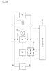
《第3実施形態》
図10は、発明の他の実施形態に係る電源制御装置のブロック図である。本例では上述した第1実施形態に対して、スイッチ回路3と放電回路6を連動させる構成が異なる。これ以外の構成は上述した第1実施形態と同じであり、第1実施形態又は第2実施形態の記載を適宜、援用する。
<< Third Embodiment >>
FIG. 10 is a block diagram of a power supply control device according to another embodiment of the invention. In this example, the structure which makes the
図10に示すように、電源制御装置は、電源1と、電力変換器2と、コンデンサ5と、放電回路6と、コントローラ10と、スイッチ回路11と、信号発生器12と、電圧センサ13と、電源ラインP、Nを備えている。
As shown in FIG. 10, the power supply control device includes a
スイッチ回路11は、機械式リレー又は半導体スイッチ等により構成されている。スイッチ回路11は、主電源1と電力変換器2との間で、電源ラインNに接続されている。スイッチ回路11は、ノーマリオフのスイッチである。
The
信号発生器12は、放電回路6の導通状態と遮断状態を切り替えるための信号を発生し、放電回路6に出力する。信号発生器12はコントローラ10により制御されている。電圧センサ13は、放電回路6に対して並列に接続されており、放電回路6の両端の電圧を検出する。電圧センサ13の検出電圧はコントローラ10に出力される。
The
コントローラ10は、放電回路6の導通状態から遮断状態の切り替わりに対して、スイッチ回路11の遮断状態から導通状態への切り替わりを連動させる。また、コントローラ10は、放電回路6の遮断状態から導通状態の切り替わりに対して、スイッチ回路11の導通状態から遮断状態への切り替わりを連動させる。コントローラ10は、電圧センサ13を用いて、放電回路6の導通状態及び遮断状態を検出する。そして、コントローラ10は、放電回路6の導通状態から遮断状態への切り替わりを検出した場合には、スイッチ回路11を遮断状態から導通状態に切り替える。また、コントローラ10は、放電回路6の遮断状態から導通状態への切り替わりを検出した場合には、スイッチ回路11を導通状態から遮断状態に切り替える。すなわち、コントローラ10は、センサ13を用いて、放電回路6の状態(導通状態、遮断状態)を判断しつつ、その判断結果に基づいてスイッチ回路11の状態を切り替えることで、放電回路6とスイッチ回路11とを連動させている。
The
次に、図11を用いて、放電回路6とスイッチ回路11の動作を説明する。図2は、信号発生器12から出力される信号の特性、放電回路6の状態、及び、スイッチ回路11の状態を説明するためのグラフである。信号発生器12の出力信号は、ローレベルで非放電指示を示し、ハイレベルで放電指示を示している。放電指示は、放電回路6を導通状態にするための指示である。非放電指示は、放電回路6を開放状態にするための指示である。そして、図11で示した、放電回路6のグラフの縦軸の表示及びスイッチ回路11のグラフの縦軸の表示は、図2と同様である。なお、電圧センサ13の検出電圧の特性は、図11に示す放電回路の特性とは逆の特性で推移する。
Next, the operation of the
初期状態として、放電回路6は導通状態であり、コンデンサ5が放電されている状態である。また、スイッチ回路11は遮断状態(開放)である。
As an initial state, the
まず、コントローラ10は、信号発生器12から非放電指示を示す信号を出力するように、信号発生器12に対して制御信号を出力する。信号発生器は、時間t4で、信号発生器4の出力レベルを下げる。出力信号のレベルは、所定の時間遅れをもって、下がり、時間t5でローレベルになる。放電回路6は、非放電指示を示す出力信号をトリガとして、導通状態から遮断状態に切り替わる。放電回路6の開放動作に伴い、電流経路の抵抗は高くなり、電流は低下する。そして、放電回路6の入力出間の電位差が高くなる。
First, the
時間t6で、電圧センサ13の検出電圧が閾値よりも高くなる。コントローラ10は、電圧センサ13の検出電圧が閾値(Vth)より高くなった場合に、放電回路6が導通状態から遮断状態に切り替わったと検出する。閾値(Vth)は、放電回路6が導通状態から遮断状態に切り替わったことを示す値であって、放電回路6の入力間の電位差に対応した電圧値で表される。そして、コントローラ10は、時間t6で、放電回路6が導通状態から遮断状態に切り替わったことを検出し、スイッチ回路11を遮断状態から導通状態に切り替える。
At time t 6, the detection voltage of the
これにより、コントローラ10は、放電回路6の導通状態から遮断状態の切り替わりに対して、スイッチ回路11の遮断状態から導通状態への切り替わりを連動させている。
Thus, the
放電回路6が遮断状態から導通状態に切り替わる際には、まず、信号発生器12からの出力信号がローレベルからハイレベルに上がると、放電回路6は遮断状態から導通状態に切り替わる動作を行う。そして、放電回路6の動作に伴い、放電回路6の入出力間の電位差が下がる。コントローラ10は、電圧センサ13の検出電圧が閾値より低くなると、放電回路6が遮断状態から導通状態に切り替わったことを、検出する。そして、コントローラ10は、スイッチ回路11を導通状態から遮断状態に切り替える、これにより、コントローラ10は、放電回路6の遮断状態から導通状態の切り替わりに対して、スイッチ回路11の導通状態から遮断状態への切り替わりを連動させている。
When the
上記のように、本実施形態は、放電回路6の導通状態から遮断状態への切り替わりに対して、スイッチ回路11の遮断状態から導通状態への切り替わりを連動させている。これにより、電源短絡を防止できる。その結果として、放電回路の保護を図ることができ、高い冗長性を保つことができる。
As described above, in the present embodiment, the switching of the
また本実施形態は、放電回路6の遮断状態から導通状態への切り替わりに対して、スイッチ回路11の導通状態から遮断状態への切り替わりを連動させている。これにより、電源短絡を防止できる。
In the present embodiment, the switching of the
なお、本実施形態の変形例として、電源制御装置は、電圧センサ13の代わりに、電流センサを備えてもよい。電源制御装置は、電圧センサ13及び電流センサを備えてもよい。
As a modification of this embodiment, the power supply control device may include a current sensor instead of the
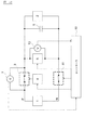
《第4実施形態》
図12は、発明の他の実施形態に係る電源制御装置のブロック図である。本例では上述した第1実施形態に対して、スイッチ回路3と放電回路6を連動させる構成が異なる。これ以外の構成は上述した第1実施形態と同じであり、第1〜第3実施形態の記載を適宜、援用する。
<< 4th Embodiment >>
FIG. 12 is a block diagram of a power supply control device according to another embodiment of the invention. In this example, the structure which makes the
図12に示すように、電源制御装置は、電源1と、電力変換器2と、スイッチ回路3と、信号発生器4と、コンデンサ5と、放電回路6と、電圧センサ7と、コントローラ10と、スイッチ回路11と、電圧センサ13と、電源ラインP、Nを備えている。スイッチ回路11及び電圧センサ13の接続位置は、第3実施形態と同様である。
As shown in FIG. 12, the power supply control device includes a
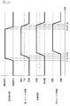
次に、図13を用いて、スイッチ回路3と放電回路6の動作を説明する。図2は、信号発生器4から出力される信号の特性、スイッチ回路3(第1スイッチ回路)の状態、放電回路6の状態、及びスイッチ回路11(第2スイッチ回路)を説明するためのグラフである。信号発生器4の出力信号は、ローレベルで接続指示を示し、ハイレベルで開放指示を示している。接続指示は、スイッチ回路3を導通状態にするための指示である。開放指示は、スイッチ回路3を開放状態にするための指示である。そして、図13で示した、放電回路6のグラフの縦軸の表示及びスイッチ回路3、11のグラフの縦軸の表示は、図2と同様である。なお、電圧センサ13の検出電圧の特性は、図13に示す放電回路の特性とは逆の特性で推移する。
Next, the operation of the
初期状態として、スイッチ回路3、11は導通状態であり、主電源1は電力変換器2に対して電力を供給しており、コンデンサ5はチャージされた状態である。また、放電回路6は遮断状態である。時間t1〜時間t3までのコントローラ10の制御シーケンスは、第1実施形態と同様であり、説明を省略する。
As an initial state, the
時間t3以降、放電回路6が遮断状態から導通状態に切り替わり、電圧センサ13の検出電圧が低くなる。時間t4で、電圧センサ13の検出電圧が閾値よりも低くなる。コントローラ10は、時間t4で、電圧センサ13の検出電圧が閾値より低くなった場合に、放電回路6が遮断状態から導通状態に切り替わったと検出し、スイッチ回路11を導通状態から遮断状態に切り替える。
Time t 3 or later, the discharging
信号発生器4は、時間t5で、信号発生器4の信号レベルをハイレベルから下げる。信号発生器4の信号レベルは時間t6でハイレベルになる。スイッチ回路3は、接続指示を示す出力信号をトリガとして、遮断状態から導通状態に切り替わる。電圧センサ7の検出電圧は、時間t6から下降する。時間t7で、電圧センサ7の検出電圧が閾値よりも低くなる。コントローラ10は、電圧センサ7の検出電圧が閾値より低くなった場合に、スイッチ回路3が遮断状態から導通状態に切り替わったと検出し、放電回路6を導通状態から遮断状態に切り替える。時間t7以降、放電回路6が導通状態から遮断状態に切り替わり、電圧センサ13の検出電圧が高くなる。コントローラ10は、時間t8で、電圧センサ13の検出電圧が閾値より高くなった場合に、放電回路6が導通状態から遮断状態に切り替わったと検出し、スイッチ回路11を遮断状態から導通状態に切り替える。
主電源1と電力変換器2との間の電流経路を開放する場合には、スイッチ回路3が「接続」であり、放電回路6が「非放電」であり、スイッチ回路11が「接続」である状態から、スイッチ回路3が「開放」に、放電回路6が「放電」に、スイッチ回路11が「開放」になるよう、状態を順次切り替える。これにより電源短絡を防ぐことができる。
When the current path between the
主電源1と電力変換器2との間の電流経路を電気的に導通する場合には、スイッチ回路3が「開放」であり、放電回路6が「放電」であり、スイッチ回路11が「開放」である状態から、スイッチ回路3が「接続」に、放電回路6が「非放電」に、スイッチ回路11が「接続」になるよう、状態を順次切り替える。これにより電源短絡を防ぐことができる。
When the current path between the
1…主電源
2…電力変換器
3、11…スイッチ回路
4…信号発生器
5…コンデンサ
6…放電回路
7、13…電圧センサ
8、28…電流センサ
9…バイパス回路
10…コントローラ
11…スイッチ回路
12…信号発生器
20…連動回路
21…副電源
22…コイル
23…ダイオード
25…抵抗
26…電圧センサ
27…制御回路
P、N…電源ライン
DESCRIPTION OF
Claims (15)
前記一対の電源ラインの間に接続されたコンデンサと、
前記正極から前記負荷を介して前記負極までの電流経路に接続され、前記電流経路の導通及び遮断を切り替えるスイッチ回路と、
前記電源ラインに接続され、前記コンデンサを放電させる放電回路と、
前記スイッチ回路及び前記放電回路の一方の回路である第1回路と、前記スイッチ回路及び前記スイッチ回路の他方の回路である第2回路とを連動させる連動手段を備え、
前記連動手段は、前記第1回路の導通状態から放電状態への切り替わりに対して、前記第2回路を遮断状態から導通状態への切り替わりを連動させる電源制御装置。 A main power source that is electrically connected to a load by a pair of power supply lines and has a positive electrode and a negative electrode;
A capacitor connected between the pair of power lines;
A switch circuit that is connected to a current path from the positive electrode through the load to the negative electrode and switches between conduction and interruption of the current path;
A discharge circuit connected to the power supply line and discharging the capacitor;
A linking means for interlocking a first circuit that is one of the switch circuit and the discharge circuit and a second circuit that is the other circuit of the switch circuit and the switch circuit;
The interlocking unit is a power supply control device that interlocks the switching of the second circuit from the cutoff state to the conducting state with respect to the switching of the first circuit from the conducting state to the discharging state.
前記連動手段は、
導通状態から遮断状態への前記スイッチ回路の切り替わりに連動して、前記放電回路を遮断状態から導電状態に切り替える
請求項1記載の電源制御装置。 The discharge circuit is a circuit that discharges the capacitor in a conductive state and does not discharge the capacitor in a cut-off state;
The interlocking means is
The power supply control device according to claim 1, wherein the discharge circuit is switched from the cutoff state to the conductive state in conjunction with the switching of the switch circuit from the conduction state to the cutoff state.
前記連動手段は、
導通状態から遮断状態への前記放電回路の切り替わりに連動して、前記スイッチ回路を遮断状態から導電状態に切り替える
請求項1又は2記載の電源制御装置。 The discharge circuit is a circuit that discharges the capacitor in a conductive state and does not discharge the capacitor in a cut-off state;
The interlocking means is
The power supply control device according to claim 1 or 2, wherein the switch circuit is switched from the cut-off state to the conductive state in conjunction with the switching of the discharge circuit from the conductive state to the cut-off state.
前記連動手段は、
前記センサを用いて前記第1回路の導通状態及び遮断状態を検出し、
前記第1回路の遮断状態を検出した場合に、前記第2回路を遮断状態から導通状態に切り替える
請求項1〜3のいずれか一項に記載の電源制御装置。 A sensor for detecting a current or voltage in the current path;
The interlocking means is
Detecting the conduction state and the interruption state of the first circuit using the sensor,
The power supply control device according to any one of claims 1 to 3, wherein when the interrupted state of the first circuit is detected, the second circuit is switched from the interrupted state to a conductive state.
前記連動手段は、前記主電源の電力が供給されている場合には前記放電回路を遮断状態とし、前記主電源の電力が供給されていない場合には前記放電回路を導通状態とする回路である
請求項1〜4のいずれか一項に記載の電源制御装置。 The power of the main power supply is supplied to the interlocking means via the switch circuit,
The interlocking unit is a circuit that shuts off the discharge circuit when the power of the main power supply is supplied and turns the discharge circuit on when the power of the main power supply is not supplied. The power supply control apparatus as described in any one of Claims 1-4.
副電源を有し、かつ、
前記副電源の電流が前記連動手段の内部回路を流れる場合には、前記放電回路を遮断状態とし、前記副電源の電流が前記内部回路を流れない場合には、前記放電回路を導通状態とする回路である
請求項1〜4のいずれか一項に記載の電源制御装置。 The interlocking means is
Has a secondary power supply, and
When the current of the sub power source flows through the internal circuit of the interlocking means, the discharge circuit is turned off, and when the current of the sub power source does not flow through the internal circuit, the discharge circuit is turned on. It is a circuit, The power supply control apparatus as described in any one of Claims 1-4.
請求項6記載の電源制御装置。 The power supply control device according to claim 6, wherein a positive electrode of the sub power supply is connected to the power supply line on the positive electrode side, or a negative electrode of the sub power supply is connected to the power supply line on the negative electrode side.
前記ダイオードのカソード端子は配線により前記電源ラインに接続されている
請求項5〜7のいずれか一項に記載の電源制御装置。 The interlocking means has a diode,
The power supply control device according to claim 5, wherein a cathode terminal of the diode is connected to the power supply line by wiring.
請求項8記載の電源制御装置。 The power supply control device according to claim 8, wherein a breakdown voltage of the diode is equal to or higher than an output voltage of the main power supply.
請求項1〜9のいずれか一項に記載の電源制御装置。 The power supply control device according to claim 1, wherein the switch circuit includes a mechanical relay.
請求項1〜9のいずれか一項に記載の電源制御装置。 The power supply control device according to claim 1, wherein the switch circuit includes a semiconductor switch.
請求項1〜11のいずれか一項に記載の電源制御装置。 The power supply control device according to any one of claims 1 to 11, wherein the switch circuit is in a cut-off state when there is no power request from the main power supply to the load.
請求項1〜12のいずれか一項に記載の電源制御装置。 The power supply control device according to claim 1, wherein the discharge circuit includes a mechanical relay.
請求項1〜12のいずれか一項に記載の電源制御装置。 The power supply control device according to any one of claims 1 to 12, wherein the discharge circuit includes a semiconductor switch circuit.
請求項1〜14のいずれか一項に記載の電源制御装置。 The power supply control device according to any one of claims 1 to 14, wherein the discharge circuit is in a conductive state when there is no power request from the main power supply to the load.
Priority Applications (1)
| Application Number | Priority Date | Filing Date | Title |
|---|---|---|---|
| JP2015046957A JP2016167929A (en) | 2015-03-10 | 2015-03-10 | Power supply controller |
Applications Claiming Priority (1)
| Application Number | Priority Date | Filing Date | Title |
|---|---|---|---|
| JP2015046957A JP2016167929A (en) | 2015-03-10 | 2015-03-10 | Power supply controller |
Publications (1)
| Publication Number | Publication Date |
|---|---|
| JP2016167929A true JP2016167929A (en) | 2016-09-15 |
Family
ID=56897952
Family Applications (1)
| Application Number | Title | Priority Date | Filing Date |
|---|---|---|---|
| JP2015046957A Pending JP2016167929A (en) | 2015-03-10 | 2015-03-10 | Power supply controller |
Country Status (1)
| Country | Link |
|---|---|
| JP (1) | JP2016167929A (en) |
Citations (3)
| Publication number | Priority date | Publication date | Assignee | Title |
|---|---|---|---|---|
| JP2001157359A (en) * | 1999-11-26 | 2001-06-08 | Toyo Electric Mfg Co Ltd | Method of preventing arc for breaker of power converter |
| JP2010206909A (en) * | 2009-03-03 | 2010-09-16 | Hitachi Automotive Systems Ltd | Power conversion apparatus |
| JP2012231627A (en) * | 2011-04-27 | 2012-11-22 | Toyo Electric Mfg Co Ltd | Arc prevention method for breaker for power conversion device |
-
2015
- 2015-03-10 JP JP2015046957A patent/JP2016167929A/en active Pending
Patent Citations (3)
| Publication number | Priority date | Publication date | Assignee | Title |
|---|---|---|---|---|
| JP2001157359A (en) * | 1999-11-26 | 2001-06-08 | Toyo Electric Mfg Co Ltd | Method of preventing arc for breaker of power converter |
| JP2010206909A (en) * | 2009-03-03 | 2010-09-16 | Hitachi Automotive Systems Ltd | Power conversion apparatus |
| JP2012231627A (en) * | 2011-04-27 | 2012-11-22 | Toyo Electric Mfg Co Ltd | Arc prevention method for breaker for power conversion device |
Similar Documents
| Publication | Publication Date | Title |
|---|---|---|
| JP6877338B2 (en) | Power control device and its method | |
| CN111226364B (en) | Power supply device, power control device, and relay determination method for power supply device | |
| CN108028547B (en) | Power supply device and switch control method thereof | |
| JP2019075851A (en) | Motor driving device with failure detection function | |
| JP5875214B2 (en) | Power conversion system | |
| JP2013172632A (en) | Power conversion device | |
| CN108701556B (en) | DC voltage switch | |
| CN107852024B (en) | Power supply unit and reverse feeding protection method thereof | |
| US7944089B2 (en) | Uninterruptible power supply module | |
| JP2018182852A (en) | Converter device provided with fault detection function of power element and fault detection method of power element | |
| KR102351067B1 (en) | Power supply aparatus for electric vehicle and power supply method using it | |
| JP6973739B2 (en) | Control system that switches the DC-DC voltage converter from boost operation mode to safe operation mode | |
| JP6495554B2 (en) | Control system for switching DC-DC voltage converter from buck operation mode to safe operation mode | |
| CN116114163A (en) | Arrangement and method for discharging a DC link capacitor | |
| JP5611300B2 (en) | Power converter and control method thereof | |
| JP2004112929A (en) | Ac-dc converter | |
| JP2008104276A (en) | Inverter device | |
| JP5115064B2 (en) | Robot controller | |
| JP2016167929A (en) | Power supply controller | |
| JP6955951B2 (en) | Discharge device | |
| JP2015050825A (en) | Discharge control device | |
| JP2019530399A (en) | Uninterruptible power supply control method and uninterruptible power supply equipment | |
| CN108808834B (en) | On-line uninterrupted power supply and control method thereof | |
| JP6815762B2 (en) | Power conversion system | |
| JP5764680B2 (en) | Inrush current prevention device |
Legal Events
| Date | Code | Title | Description |
|---|---|---|---|
| A621 | Written request for application examination |
Free format text: JAPANESE INTERMEDIATE CODE: A621 Effective date: 20180126 |
|
| A131 | Notification of reasons for refusal |
Free format text: JAPANESE INTERMEDIATE CODE: A131 Effective date: 20181030 |
|
| A977 | Report on retrieval |
Free format text: JAPANESE INTERMEDIATE CODE: A971007 Effective date: 20181031 |
|
| A521 | Request for written amendment filed |
Free format text: JAPANESE INTERMEDIATE CODE: A523 Effective date: 20181228 |
|
| A02 | Decision of refusal |
Free format text: JAPANESE INTERMEDIATE CODE: A02 Effective date: 20190604 |