JP6877338B2 - Power control device and its method - Google Patents
Power control device and its method Download PDFInfo
- Publication number
- JP6877338B2 JP6877338B2 JP2017518681A JP2017518681A JP6877338B2 JP 6877338 B2 JP6877338 B2 JP 6877338B2 JP 2017518681 A JP2017518681 A JP 2017518681A JP 2017518681 A JP2017518681 A JP 2017518681A JP 6877338 B2 JP6877338 B2 JP 6877338B2
- Authority
- JP
- Japan
- Prior art keywords
- power supply
- relay
- switching element
- current path
- control device
- Prior art date
- Legal status (The legal status is an assumption and is not a legal conclusion. Google has not performed a legal analysis and makes no representation as to the accuracy of the status listed.)
- Active
Links
Images


Classifications
-
- H—ELECTRICITY
- H02—GENERATION; CONVERSION OR DISTRIBUTION OF ELECTRIC POWER
- H02M—APPARATUS FOR CONVERSION BETWEEN AC AND AC, BETWEEN AC AND DC, OR BETWEEN DC AND DC, AND FOR USE WITH MAINS OR SIMILAR POWER SUPPLY SYSTEMS; CONVERSION OF DC OR AC INPUT POWER INTO SURGE OUTPUT POWER; CONTROL OR REGULATION THEREOF
- H02M1/00—Details of apparatus for conversion
- H02M1/36—Means for starting or stopping converters
-
- H—ELECTRICITY
- H01—ELECTRIC ELEMENTS
- H01H—ELECTRIC SWITCHES; RELAYS; SELECTORS; EMERGENCY PROTECTIVE DEVICES
- H01H9/00—Details of switching devices, not covered by groups H01H1/00 - H01H7/00
- H01H9/54—Circuit arrangements not adapted to a particular application of the switching device and for which no provision exists elsewhere
- H01H9/548—Electromechanical and static switch connected in series
-
- G—PHYSICS
- G01—MEASURING; TESTING
- G01R—MEASURING ELECTRIC VARIABLES; MEASURING MAGNETIC VARIABLES
- G01R31/00—Arrangements for testing electric properties; Arrangements for locating electric faults; Arrangements for electrical testing characterised by what is being tested not provided for elsewhere
- G01R31/26—Testing of individual semiconductor devices
- G01R31/2607—Circuits therefor
- G01R31/2621—Circuits therefor for testing field effect transistors, i.e. FET's
-
- G—PHYSICS
- G01—MEASURING; TESTING
- G01R—MEASURING ELECTRIC VARIABLES; MEASURING MAGNETIC VARIABLES
- G01R31/00—Arrangements for testing electric properties; Arrangements for locating electric faults; Arrangements for electrical testing characterised by what is being tested not provided for elsewhere
- G01R31/327—Testing of circuit interrupters, switches or circuit-breakers
- G01R31/3277—Testing of circuit interrupters, switches or circuit-breakers of low voltage devices, e.g. domestic or industrial devices, such as motor protections, relays, rotation switches
- G01R31/3278—Testing of circuit interrupters, switches or circuit-breakers of low voltage devices, e.g. domestic or industrial devices, such as motor protections, relays, rotation switches of relays, solenoids or reed switches
-
- G—PHYSICS
- G01—MEASURING; TESTING
- G01R—MEASURING ELECTRIC VARIABLES; MEASURING MAGNETIC VARIABLES
- G01R31/00—Arrangements for testing electric properties; Arrangements for locating electric faults; Arrangements for electrical testing characterised by what is being tested not provided for elsewhere
- G01R31/44—Testing lamps
-
- H—ELECTRICITY
- H01—ELECTRIC ELEMENTS
- H01H—ELECTRIC SWITCHES; RELAYS; SELECTORS; EMERGENCY PROTECTIVE DEVICES
- H01H47/00—Circuit arrangements not adapted to a particular application of the relay and designed to obtain desired operating characteristics or to provide energising current
- H01H47/001—Functional circuits, e.g. logic, sequencing, interlocking circuits
-
- H—ELECTRICITY
- H02—GENERATION; CONVERSION OR DISTRIBUTION OF ELECTRIC POWER
- H02H—EMERGENCY PROTECTIVE CIRCUIT ARRANGEMENTS
- H02H3/00—Emergency protective circuit arrangements for automatic disconnection directly responsive to an undesired change from normal electric working condition with or without subsequent reconnection ; integrated protection
- H02H3/02—Details
- H02H3/04—Details with warning or supervision in addition to disconnection, e.g. for indicating that protective apparatus has functioned
- H02H3/044—Checking correct functioning of protective arrangements, e.g. by simulating a fault
-
- H—ELECTRICITY
- H02—GENERATION; CONVERSION OR DISTRIBUTION OF ELECTRIC POWER
- H02J—CIRCUIT ARRANGEMENTS OR SYSTEMS FOR SUPPLYING OR DISTRIBUTING ELECTRIC POWER; SYSTEMS FOR STORING ELECTRIC ENERGY
- H02J7/00—Circuit arrangements for charging or depolarising batteries or for supplying loads from batteries
- H02J7/0029—Circuit arrangements for charging or depolarising batteries or for supplying loads from batteries with safety or protection devices or circuits
- H02J7/0031—Circuit arrangements for charging or depolarising batteries or for supplying loads from batteries with safety or protection devices or circuits using battery or load disconnect circuits
-
- H—ELECTRICITY
- H02—GENERATION; CONVERSION OR DISTRIBUTION OF ELECTRIC POWER
- H02M—APPARATUS FOR CONVERSION BETWEEN AC AND AC, BETWEEN AC AND DC, OR BETWEEN DC AND DC, AND FOR USE WITH MAINS OR SIMILAR POWER SUPPLY SYSTEMS; CONVERSION OF DC OR AC INPUT POWER INTO SURGE OUTPUT POWER; CONTROL OR REGULATION THEREOF
- H02M1/00—Details of apparatus for conversion
- H02M1/0003—Details of control, feedback or regulation circuits
- H02M1/0009—Devices or circuits for detecting current in a converter
-
- H—ELECTRICITY
- H02—GENERATION; CONVERSION OR DISTRIBUTION OF ELECTRIC POWER
- H02M—APPARATUS FOR CONVERSION BETWEEN AC AND AC, BETWEEN AC AND DC, OR BETWEEN DC AND DC, AND FOR USE WITH MAINS OR SIMILAR POWER SUPPLY SYSTEMS; CONVERSION OF DC OR AC INPUT POWER INTO SURGE OUTPUT POWER; CONTROL OR REGULATION THEREOF
- H02M1/00—Details of apparatus for conversion
- H02M1/32—Means for protecting converters other than automatic disconnection
-
- H—ELECTRICITY
- H02—GENERATION; CONVERSION OR DISTRIBUTION OF ELECTRIC POWER
- H02J—CIRCUIT ARRANGEMENTS OR SYSTEMS FOR SUPPLYING OR DISTRIBUTING ELECTRIC POWER; SYSTEMS FOR STORING ELECTRIC ENERGY
- H02J2207/00—Indexing scheme relating to details of circuit arrangements for charging or depolarising batteries or for supplying loads from batteries
- H02J2207/20—Charging or discharging characterised by the power electronics converter
Description
本発明は、電源制御装置及びその方法に関するものである。 The present invention relates to a power supply control device and a method thereof.
突入電流を防止するための制限抵抗を廃止した電源制御装置が開示されている。当該電源制御装置において、制御装置は、起動指令STを受けると、システムメインリレーSMR1、SMR3をオンさせてコンデンサCを充電するプリチャージ処理を実行する。ここで、制限抵抗が設けられていないため、制御装置は、システムメインリレーSMR3のパワーMOSFETが最大定格電力を超えない範囲であって、かつ、飽和領域で動作するようにパワーMOSFETのゲート電圧を制御する。そして、プリチャージ処理の完了後に、SMR2をオンに、SMR3をオフにする(特許文献1)。 A power supply control device that eliminates the limiting resistor for preventing inrush current is disclosed. In the power supply control device, when the control device receives the start command ST, the control device executes a precharge process of turning on the system main relays SMR1 and SMR3 to charge the capacitor C. Here, since the limiting resistor is not provided, the control device sets the gate voltage of the power MOSFET so that the power MOSFET of the system main relay SMR3 does not exceed the maximum rated power and operates in the saturation region. Control. Then, after the precharge process is completed, SMR2 is turned on and SMR3 is turned off (Patent Document 1).
しかしながら、上記の電源制御装置において、バッテリとモータとの間に流れている電流を遮断する場合には、メインリレーSMR3のパワーMOSFETパワーMOSFETがオフになっている状態で、メインリレーSMR1、SMR2をオフにすることなる。そのため、電流の遮断時に、メインリレーSMR1、SMR2の接点が劣化しやすいという問題があった。 However, in the above power supply control device, when the current flowing between the battery and the motor is cut off, the main relays SMR1 and SMR2 are operated with the power MOSFET power MOSFET of the main relay SMR3 turned off. It will be turned off. Therefore, there is a problem that the contacts of the main relays SMR1 and SMR2 tend to deteriorate when the current is cut off.
本発明が解決しようとする課題は、リレー接点の劣化を抑制できる電源制御装置又はその方法を提供することである。 An object to be solved by the present invention is to provide a power supply control device or a method thereof capable of suppressing deterioration of relay contacts.
本発明は、直流電源の正極から負荷を介して直流電源の負極までの電流経路に対して、半導体スイッチング素子及びリレーをそれぞれ直列に接続し、電流経路に流れる電流が所定の電流閾値より低い状態である場合に、リレーをオフ状態にした後に半導体スイッチング素子をオフ状態に切り替えることで、電流経路を開放させることによって上記課題を解決する。 In the present invention, a semiconductor switching element and a relay are connected in series to the current path from the positive side of the DC power supply to the negative side of the DC power supply via a load, and the current flowing in the current path is lower than a predetermined current threshold value. If it is, by switching the semiconductors switching elements to the oFF state after the relay off, to solve the above problem by opening the current path.
本発明によれば、リレーには高電流が流れていない状態で、スイッチング素子より先にリレーをオフ状態に切り換えているため、リレーの接点の劣化を抑制できるという効果を奏する。 According to the present invention, since the relay is switched to the off state before the switching element in a state where a high current does not flow through the relay, it is possible to suppress the deterioration of the contact of the relay.
以下、本発明の実施形態を図面に基づいて説明する。
《第1実施形態》Hereinafter, embodiments of the present invention will be described with reference to the drawings.
<< First Embodiment >>
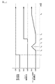
図1は、本発明の実施形態に係る電源制御装置のブロック図である。本実施形態に係る電源制御装置は、例えば車両に設けられており、車両に搭載されたバッテリの電力を、インバータを介してモータに供給するシステムを制御する装置である。以下の説明では、電源制御装置が車両に設けられる場合を前提に説明するが、電源制御装置は車両に限らず他の装置に設けられていてもよい。例えば、電源制御装置は、定置用の電源の電力を負荷に供給する際の電力システムに適用されてもよい。 FIG. 1 is a block diagram of a power supply control device according to an embodiment of the present invention. The power supply control device according to the present embodiment is, for example, a device provided in a vehicle and controls a system for supplying electric power of a battery mounted in the vehicle to a motor via an inverter. In the following description, it is assumed that the power supply control device is provided in the vehicle, but the power supply control device may be provided not only in the vehicle but also in other devices. For example, the power control unit may be applied to a power system for supplying power from a stationary power source to a load.
図1に示すように、電源制御装置は、直流電源1と、負荷装置2と、スイッチング素子3と、リレー4と、駆動制御装置5と、電圧センサ6A、6B、6Cと、電流センサ7A、7Bと、制御装置8と、電源ラインP、Nを備えている。なお、制御装置8は、必ずしも電源制御装置の構成でなくてもよい。図1では、駆動制御装置5と制御装置8を分けて図示しているが、駆動制御装置5及び制御装置8を1つの制御装置としてもよい。なお、図1において、点線の矢印は制御信号を示している。
As shown in FIG. 1, the power supply control device includes a
直流電源1は、負荷装置2に対して電力を供給する装置であって、バッテリ11と筐体12とを有している。バッテリ11は、リチウムイオン電池などの二次電池を複数接続する。バッテリ11は、正極及び負極を有している。バッテリ11の正極と負極は、一対の電源ラインP、Nを介して負荷装置2にそれぞれ接続されている。筐体12は、バッテリ11を収容するための金属製のケースである。また直流電源1は、負荷装置2の回生によって発電した電力を、バッテリ11で蓄電する機能も有している。
The
負荷装置2は、直流電源1の電力を消費する装置であり、インバータ21と筐体22とを有している。負荷装置2は電源ラインP、Nを介して、直流電源1に電気的に接続されている。インバータ21は、バッテリ11の電力を変換し、図示しないモータに変換された電力を供給する電力変換装置である。インバータ21の入力側(DC側)は、電源ラインを介してバッテリ11に接続されており、インバータ21の出力側(AC側)は、モータに接続されている。筐体22は、インバータ21を収容するための金属製のケースである。なお、負荷装置2は、インバータ21に限らず、モータを有してもよく、インバータ21以外の他の負荷(例えば、電熱線)でもよい。
The
電源ラインP、Nは、直流電源1と負荷装置2との間を接続する一対の配線である。また、電源ラインP、Nは、直流電源1の正極から負荷装置2を介して直流電源1の負極までの電流経路となる。
The power supply lines P and N are a pair of wirings connecting the
スイッチング素子3は、スイッチング機能をもつ半導体素子である。本実施形態では、スイッチング素子3はPチャンネルMOSFETである。スイッチング素子3は、−電極側(負極側)の電源ラインNに接続されている。スイッチング素子3は、MOSFETに限らずIGBTでもよい。またスイッチング素子3は、Si、SiC、又はGaN等のワイドバンドギャップ半導体材料を用いたユニポーラまたはバイポーラ構造のスイッチング素子でよい。
The
直流電源1から負荷装置2に向かう方向を順方向とした場合に、本実施形態に係る電源制御装置は、順方向に流れる電流を遮断できるように構成されている。そのため、PチャネルFETの導通方向が、電源ラインNの順方向となるように、スイッチング素子3は接続されている。なお、スイッチング素子3を用いて、逆方向の回生電流を遮断するように構成する場合には、図1に示すスイッチング素子3のドレインとソースを逆にした上で、スイッチング素子3を接続すればよい。
When the direction from the
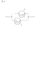
また順方向及び逆方向の電流を遮断する場合には、図2に示すように、逆耐圧性能をもたない複数のスイッチング素子3を直列に接続すればよい。図2は、両方向の電流の遮断を可能とするスイッチング素子3の接続例を示した回路図である。図2に示すように、2つのスイッチング素子3は、P型チャネルのMOSFETであり、互いに逆方向にしつつ、直列に接続されている。
Further, when interrupting the currents in the forward direction and the reverse direction, as shown in FIG. 2, a plurality of
また、両方向の電流の遮断を可能とする他の接続例として、図3に示すように、逆耐圧性能をもつスイッチング素子3を並列に接続してもよい。図3は、両方向の電流の遮断を可能とするスイッチング素子3の接続例を示した回路図である。図3に示すように、2つのスイッチング素子3は、IGBTであり、互いに逆方向にしつつ、並列に接続されている。
Further, as another connection example capable of interrupting the current in both directions, as shown in FIG. 3, switching
リレー4は機械式のスイッチである。リレー4には、例えば電磁継電器が用いられる。リレー4は、スイッチング素子3と異なり、スイッチのオン、オフに伴って、機械的に移動する一対の接点を有している。一対の接点のうち、少なくとも一方の接点が動的に移動すればよい。リレー4は、+電極側(正極側)の電源ラインPに接続されている。リレー4は、コイルを有しており、当該コイルに電流を流すことで生じる電磁誘導によって、接点が駆動するような構造になっている。
The relay 4 is a mechanical switch. For the relay 4, for example, an electromagnetic relay is used. Unlike the
上記のように、本実施形態に係る電源制御装置において、直流電源1と負荷装置2との間で電流を導通させる電流経路は、電源ラインP、Nで形成されている。電流経路の電気的な導通と遮断を切り替えるために、電源ラインP、Nにリレー4とスイッチング素子3がそれぞれ接続されている。通常、高電圧である直流電源と負荷との間で、オン、オフを切り替える場合には、一対のリレースイッチを、正極側の電源ラインと、負極側の電源ラインに接続する。一方、本願発明では、正極側に接続したリレースイッチの役割を、リレー4にもたせており、負極側に接続したリレースイッチの役割を、スイッチング素子3にもたせている。言い替えると、本実施形態において、リレー4は、正極又は負極のいずれか一方の極の電流経路を、独立してオン、オフの切り替えを可能とするスイッチである。
As described above, in the power supply control device according to the present embodiment, the current paths for conducting the current between the
バッテリ11の正極と筐体12との間の電位差(以下、第1電位差と称す)と、バッテリ11の負極と筐体との間の電位差(以下、第2電位差と称す)が異なる場合には、スイッチング素子3は、より小さい方の電位差をもつ電極側に、近づくように接続されている。例えば、第2電位差が第1電位差よりも小さい場合には、スイッチング素子3は負極側の電源ラインNに接続され、リレー4は正極側の電源ラインPに接続される。このような接続形態は、図1に示した接続形態である。一方、第1電位差が第2電位差よりも小さい場合には、スイッチング素子3は正極側の電源ラインPに接続され、リレー4は負極側の電源ラインNに接続される。
When the potential difference between the positive electrode of the
スイッチング素子3は、オフ状態でも、素子の内部でリーク電流が発生する可能性がある。そして、電圧が高いほど、リーク電流が増加する。そのため、第1電位差と第2電位差のうち、電位差の低い方の電源ラインに、スイッチング素子3を接続することで、筐体等からスイッチング素子3に流れるリーク電流を抑制することができる。
Even in the off state of the
駆動制御装置5は、スイッチング素子3及びリレー4のオン、オフを制御するコントローラである。駆動制御装置5は、制御装置8から送信される電力供給許可信号に基づき、スイッチング素子3及びリレー4のオン、オフを切り替える。また、駆動制御装置5は、電圧センサ6A〜6C、電流センサ7A、7Bの検出値に基づき、スイッチング素子3及びリレー4のオン、オフを切り替える。また、駆動制御装置5は、スイッチング素子3及びリレー4の自己診断機能も有している。
The drive control device 5 is a controller that controls on / off of the
電圧センサ6Aは、直流電源1と負荷装置2との間の電流経路のうち、入力側の電圧を検出する。電圧センサ6Aの両端子のうち、高電位側の端子は、バッテリ11の正極とリレー4との間で、電源ラインPに接続されており、低電位側の端子は、電源ラインNに接続されている。
The
電圧センサ6Bは、直流電源1と負荷装置2との間の電流経路のうち、出力側の電圧を検出する。電圧センサ6Bの両端子のうち、高電位側の端子は、リレー4とのインバータ21間で、電源ラインPに接続されており、低電位側の端子は、スイッチング素子3とインバータ21との間で、電源ラインNに接続されている。
The
電圧センサ6Cは、直流電源1と負荷装置2との間の電流経路のうち、リレー4の出力側の電圧を検出する。電圧センサ6Cの両端子のうち、高電位側の端子は、リレー4とのインバータ21間で、電源ラインPに接続されており、低電位側の端子は、スイッチング素子3とバッテリ11の負極との間で、電源ラインNに接続されている。
The
電流センサ7Aは、電源ラインPの電流を検出するセンサであって、バッテリ11の正極とリレー4との間で、電源ラインPに接続されている。電流センサ7Bは、電源ラインNの電流を検出するセンサであって、バッテリ11の負極とスイッチング素子3との間で、電源ラインNに接続されている。
The
電圧センサ6A、6B、6Cの検出電圧及び電流センサ7A、7Bの検出電流は、駆動制御装置5に出力される。
The detection voltage of the
制御装置8は、車両全体を制御するコントローラである。制御装置8は、駆動制御装置5との間で制御信号の通信を行うことができる。また制御装置8は、車両のメインスイッチの状態に応じて電力供給許可信号を駆動制御装置5に送信する。電力供給許可信号がオンのときには、直流電源1から負荷装置2への電力の供給が許可されたことを示す。電力供給許可信号がオフのときには、直流電源1から負荷装置2への電力の供給が許可されていないことを示す。そして、制御装置8は、例えば、ユーザの操作により車両のメインスイッチがオフからオンに切り替わった場合には、電力許可信号のレベルをハイにすることで、オン状態にする。一方、メインスイッチがオンからオフに切り替わった場合には、制御装置8は、電力許可信号のレベルをローにすることで、オフ状態にする。
The
次に、駆動制御装置5の具体的な制御について、説明する。まず、電源制御装置の立ち上げ時(起動時)の制御を説明する。駆動制御装置5は、直流電源1と負荷装置2との間の電流経路を電気的に導通させることで、電力供給のためのシステムを起動させる。具体的には、駆動制御装置5は、制御装置8から、オン状態の電流許可信号を受信した場合に、直流電源1と負荷装置2との間の電流経路を電気的に導通させるように、以下のシーケンスで制御を行う。
Next, the specific control of the drive control device 5 will be described. First, the control at the time of starting up (starting up) of the power supply control device will be described. The drive control device 5 activates the system for power supply by electrically conducting the current path between the
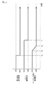
図4は、直流電源1と負荷装置2との間の電流経路を電気的に導通させる場合の、電力供給信号のオン、オフ状態、リレー4の駆動電圧、及び、スイッチング素子3の駆動電圧の特性を示すグラフである。図4のグラフの横軸は時間を示している。また、リレー4の駆動電圧は、駆動制御装置5の制御信号に基づき、リレー4のコイルに印加される電圧を示しており、駆動電圧がVONのときに、リレー4はオン状態となり、駆動電圧がVOFFのときに、リレー4はオフ状態となる。スイッチング素子3の駆動電圧は、スイッチング素子3のゲート電圧に相当する。なお、後述する図5〜図9に示すグラフの縦軸及び横軸は、図4に示すグラフの縦軸及び横軸と同様である。FIG. 4 shows the on / off state of the power supply signal, the drive voltage of the relay 4, and the drive voltage of the
電力供給信号がオフの場合に、スイッチング素子3及びリレー4はオフ状態である。すなわち、直流電源1と負荷装置2との間で電流を流す必要がない場合には、スイッチング素子3及びリレー4が共にオフ状態を維持する。これにより、電流経路のインピーダンスが高い状態で保たれ、システムの安全性を高めることができる。なお、スイッチング素子3及びリレー4のうち、いずれか一方のスイッチをオフ状態にすることで、電流経路の高インピーダンスを保つことができる場合には、スイッチング素子3及びリレー4のうち、いずれか一方のみをオフ状態にするだけもよい。
When the power supply signal is off, the switching
図4に示すように、初期状態で、電力供給信号がオフになっており、リレー4の駆動電圧及びスイッチング素子3の駆動電圧はVOFFである。時間t1で、電力供給信号がオフからオンに切り替わると、駆動制御装置5は、時間t1から所定時間の経過後の時間t2で、リレー4の駆動電圧をVOFFからVONに上げることで、リレー4をオフ状態からオン状態に切り替える。駆動制御装置5は、時間t2から所定時間の経過後の時間t3で、スイッチング素子3の駆動電圧をVOFFから上昇させる。そして、時間t4でスイッチング素子3の駆動電圧はVONとなり、スイッチング素子3はオン状態に切り替わる。As shown in FIG. 4, the power supply signal is turned off in the initial state, and the drive voltage of the relay 4 and the drive voltage of the
ところで、電流経路を電気的に導通させて、直流電源1から負荷装置2に電力を供給する場合に、電流は、電位の高いところから低いところに流れる。そして、電位の低いところに寄生容量や、容量成分をもつ回路素子が接続されている場合、例えば、負荷装置2の入力側(DC側)に平滑用のコンデンサが接続されている場合、電流経路を電気的に導通させる際の初期段階で、直流電源1から負荷装置2に突入電流が流れてしまう。そして、突入電流は、電流経路のインピーダンスが低いほど大きくなる。大きな突入電流が、リレー4に流れた場合には、リレー4の接点の固着やスイッチング素子3の素子への悪影響を誘発する。また、電流経路のインダクタンスと突入電流によって、サージ電圧が発生するおそれもある。そのため、電流経路を電気的に導通させる場合には、直流電源1から電流経路に流れる電流に制限をかけつつ、直流電源1と負荷装置2との間で電流を流さなければならない。
By the way, when electric power is supplied from the
上記のように、本実施形態において、電流経路を電気的に導通させる場合には、駆動制御装置5は、リレー4をオン状態に切り替えた後に、スイッチング素子3をオン状態に切り替える。スイッチング素子3は、MOSFETであるため、駆動制御装置5はゲート電圧を制御することで、スイッチング素子3のオン抵抗を調整することができ、電流経路に流れる電流量を任意に変更できる。リレー4は、時間t3の時点で既にオンに状態になっている。そのため、スイッチング素子3のオン抵抗が高くなるように、ゲート電圧を調整しつつ、スイッチング素子3をオン状態に切り替えることで、直流電源1から電流経路に流れ込む突入電流を抑制できる。As described above, in the case of electrically conducting the current path in the present embodiment, the drive control device 5 switches the relay 4 to the on state and then switches the switching
また、本実施形態では時間t3から徐々にスイッチング素子3の駆動電圧を低い状態から上昇させている。これにより、スイッチング素子3のオン抵抗が高い状態から徐々に低い状態に調整することができるため、突入電流を抑制することができる。Also gradually increased driving voltage of the
なお、時間t3から時間t4の期間において、駆動制御装置5は、電圧センサ6A〜6C又は電流センサ7A、7Bを用いて、直流電源1から電流経路に流れる電流を管理しつつ、突入電流を防止するための最適なゲート電圧を調整してもよい。直流電源1から電流経路に流れる電流は、例えば電圧センサ6Aの検出電圧と電圧センサ6Bの検出電圧の電圧差、電圧センサ6Cの検出電圧、又は、電流センサ7A、7Bの検出電流から検出できる。In the period from time t 3 to time t 4 , the drive control device 5 uses the
ゲート電圧を調整する際には、電流経路に流れる電流が、電流経路に接続された各素子の許容電流値を超えないように、駆動制御装置5は、ゲート電圧を調整するとよい。また、駆動制御装置5は、電流経路に流れることで、各素子の温度が許容温度より高くならないように、又は、各素子の印加電圧が許容値より高くなるように、ゲート電圧を調整するとよい。各素子の温度及び電圧は、別途センサを設け、当該センサの検出値で管理してもよく、又は、電圧センサ6A〜6C等の検出値から演算により推定値を求めることで、管理されてもよい。また、調整する際のゲート電圧の値は、予め設定されてもよく、又は、センサの検出値に基づきリアルタイムで設定してもよい。
When adjusting the gate voltage, the drive control device 5 may adjust the gate voltage so that the current flowing in the current path does not exceed the permissible current value of each element connected to the current path. Further, the drive control device 5 may adjust the gate voltage so that the temperature of each element does not become higher than the permissible temperature or the applied voltage of each element becomes higher than the permissible value by flowing in the current path. .. The temperature and voltage of each element may be controlled by a separate sensor provided and the detected value of the sensor, or may be controlled by obtaining an estimated value by calculation from the detected values of the
なお、時間t1から時間t2までの所定時間、及び、時間t2から時間t3までの所定時間が短いほど、システムの立ち上げ時間を短くすることができる。The shorter the predetermined time from time t 1 to time t 2 and the predetermined time from time t 2 to time t 3 , the shorter the system startup time can be.
本実施形態では、駆動制御装置5は、電力供給のシステムを起動させる際に、スイッチング素子3及びリレー4の自己診断を行うこともできる。図5を用いて、駆動制御装置5の制御シーケンスを説明する。
In the present embodiment, the drive control device 5 can also perform self-diagnosis of the
図5は、直流電源1と負荷装置2との間の電流経路を電気的に導通させつつ、スイッチング素子3及びリレー4の自己診断を行う場合の、電力供給信号のオン、オフの状態、リレー4の駆動電圧、及び、スイッチング素子3の駆動電圧の特性を示すグラフである。
FIG. 5 shows an on / off state of a power supply signal and a relay when self-diagnosis of the
初期状態では、電力供給信号がオフになっており、リレー4の駆動電圧及びスイッチング素子3の駆動電圧はVOFFである。時間t1で電力供給信号がオフからオンになり、時間t2でリレー4の駆動電圧がVOFFからVONに立ち上がり、時間t3でスイッチング素子3の駆動電圧がVOFFから徐々に上昇し、時間t4でスイッチング素子3の駆動電圧がVONとなる点は、図4を用いて説明した上記シーケンスの制御と同様である。In the initial state, the power supply signal is off, and the drive voltage of the relay 4 and the drive voltage of the
駆動制御装置5は、時間t1から時間t2までの所定期間内に、一時的にスイッチング素子3の駆動電圧を上げて、駆動電圧を上げた後にVOFFまで下げるように、スイッチング素子3を制御する。駆動制御装置5は、時間t1後の時間taで、スイッチング素子3の駆動電圧をVOFFから上昇させる。時間ta後の時間tbで駆動電圧がVONになると、駆動制御装置5は、スイッチング素子3の駆動電圧をVONから下げる。そして、時間tcで駆動電圧がVOFFになる。これにより、駆動制御装置5は、電流経路を導通させる場合には、リレー4をオン状態に切り替える前に、時間taから時間tcまでの期間、スイッチング素子3をオン状態にする。The drive control device 5 temporarily raises the drive voltage of the
駆動制御装置5は、時間taから時間tcまでの期間で、電圧センサ6A〜6Cの検出値又は電流センサ7A、7Bの検出値に基づき、スイッチング素子3及びリレー4の故障診断を行う。リレー4が正常であれば、時間taから時間tcまでの期間、スイッチング素子3の駆動電圧がVOFFより高くなっても、電流は直流電源1から電流経路に流れない。そのため、時間taから時間tcまでの期間中、電圧センサ6A〜6Cの検出値又は電流センサ7A、7Bの検出値に変化はなく、あるいは、変化があったとしても検出値の変動量は小さい。一方、リレー4の短絡故障(オン固着)が発生している場合には、時間taから時間tcまでの期間、スイッチング素子3の駆動電圧がVOFFより高くなると、電流が直流電源1から電流経路に流れ出す。Drive control unit 5, during a period from time t a to time t c, the detection value or the
駆動制御装置5は、時間taから時間tcまでの期間に、電圧センサ6A〜6Cの検出値又は電流センサ7A、7Bの検出値と閾値とを比較し、その比較結果に基づいて、リレー4が故障しているか否かを判断する。閾値は、リレー4の故障診断を行うために予め設定された値である。Drive control unit 5, the period from time t a to time t c, the detection value or the
駆動制御装置5は、故障診断を行う際に、電圧センサ6A〜6C及び電流センサ7A、7Bのうち、全てのセンサの検出値を用いる必要はなく、少なくとも1つの検出値を用いればよい。また、センサの検出値のうち、リレー4の故障によって、値が上昇する検出値を用いてリレー4の故障診断を行う場合には、駆動制御装置5は、検出値が閾値よりも高い場合に、リレー4が故障していると判断する。また、ンサの検出値のうち、リレー4の故障によって、値が下降する検出値を用いてリレー4の故障診断を行う場合には、駆動制御装置5は、検出値が閾値よりも低い場合に、リレー4が故障していると判断する。なお、故障診断の際の検出値の選択、及び、検出値と閾値とを比較した場合の判断基準は、リレー4の故障診断に限らず、以下に説明するスイッチング素子3の故障診断の際に適用してもよい。なお、閾値と比較される検出値は、電圧センサ6A〜6C、電流センサ7A、7Bの検出値としてもよく、これらセンサの検出値の差でもよい。
The drive control device 5 does not need to use the detection values of all the
また、時間taから時間tcまでの期間は短いほど、システムの立ち上げ時間を短くすることができ、待機電力も抑制できる。また、リレー4の短絡故障を想定すると、時間taから時間tcまでの期間に、直流電源1から電流経路に電流が流れる。そして、時間tbから時間tcの期間、電流が遮断することになるため、電流量の変化によってサージ電圧が発生するおそれがある。そのため、電流経路上の各素子の耐圧及び電流経路のインダクタンスを考慮しつつ、サージ電圧によって、悪影響が素子に及ぼさないように、時間tbから時間tcまでの期間は、できるだけ短い方が望ましい。Also, the shorter the period from the time t a to time t c, the rise time of the system can be shortened, the standby power can be suppressed. Further, assuming a short-circuit failure of the relay 4, a current flows from the
このように本実施形態において、電流経路を電気的に導通させる場合には、駆動制御装置5は、リレー4をオン状態に切り替える前に、時間tbから時間tcの期間、スイッチング素子3をオン状態にし、かつ、時間tbから時間tcの期間内に、センサの検出値に基づいて、リレー4の故障診断を行う。これにより、システムの安全性を確保しつつ、回路素子等の保護を図ることができる。As described above, in the case of electrically conducting the current path in the present embodiment, the drive control device 5 switches the switching
駆動制御装置5は、時間t2の後に、スイッチング素子3の故障診断を行うこともできる。駆動制御装置5は、時間t2から時間t3までの期間で、電圧センサ6A〜6Cの検出値又は電流センサ7A、7Bの検出値に基づき、スイッチング素子3の故障診断を行う。スイッチング素子3が正常であれば、時間t2から時間t3までの期間、リレー4がオン状態に切り替わっても、電流は直流電源1から電流経路に流れない。そして、時間t2から時間t3までの期間中、電圧センサ6A〜6Cの検出値又は電流センサ7A、7Bの検出値に変化はなく、あるいは、変化があったとしても検出値の変動量は小さい。一方、スイッチング素子3の短絡故障が発生している場合には、時間t2から時間t3までの期間、電流が直流電源1から電流経路に流れ出す。そのため、駆動制御装置5は、時間t2から時間t3までの期間、センサの検出値と予め設定された閾値とを比較しつつ、比較結果に基づきスイッチング素子3の故障を診断できる。The drive control device 5 can also perform a failure diagnosis of the
このように本実施形態において、電流経路を電気的に導通させる場合には、駆動制御装置5は、リレー4をオン状態に切り替える時点(時間t2)からスイッチング素子3をオン状態にする時点(時間t3)までの期間内に、センサの検出値に基づき、スイッチング素子3の故障診断を行う。これにより、システムの安全性を確保しつつ、回路素子等の保護を図ることができる。As described above, in the case of electrically conducting the current path in the present embodiment, the drive control device 5 starts the switching element 3 from the time when the relay 4 is switched to the on state (time t 2 ) (when the switching
また、駆動制御装置5は、時間t3の後に、スイッチング素子3及びリレー4の故障診断を行うこともできる。駆動制御装置5は、時間t3以降の所定期間で、電圧センサ6A〜6Cの検出値又は電流センサ7A、7Bの検出値に基づき、スイッチング素子3の及びリレー4の故障診断を行う。スイッチング素子3及びリレー4が正常であれば、時間t3以降、スイッチング素子3の駆動電圧の上昇に伴って、電流が直流電源1から電流経路に流れる。また、スイッチング素子3の駆動電圧がVONになった後も、電流が直流電源1から電流経路に流れる。そして、電流が直流電源1から電流経路に流れることで、電圧センサ6A〜6Cの検出値又は電流センサ7A、7Bの検出値が変化する。一方、スイッチング素子3の開放故障及びリレー4の開放故障のうち、いずれか一方の故障が発生している場合には、電流は直流電源1から電流経路に流れない。また、電圧センサ6A〜6Cの検出値又は電流センサ7A、7Bの検出値に変化はなく、あるいは、変化があったとしても検出値の変動量は小さい。そのため、駆動制御装置5は、時間t3以降の所定期間、センサの検出値と予め設定された閾値とを比較しつつ、比較結果に基づきスイッチング素子3の故障及びリレー4の故障を診断できる。The drive control unit 5, after a time t 3, it is also possible to perform failure diagnosis of the
このように、本実施形態において、電流経路を電気的に導通させる場合には、駆動制御装置5は、リレー4をオン状態に切り替えた後、センサの検出値に基づき、スイッチング素子3及びリレー4の故障診断を行う。これにより、システムの安全性を確保しつつ、回路素子等の保護を図ることができる。
As described above, in the case of electrically conducting the current path in the present embodiment, the drive control device 5 switches the relay 4 to the on state, and then the
次に、電源制御装置の立ち下げ時の制御を説明する。駆動制御装置5は、スイッチング素子3及びリレー4がオン状態で、オフ状態の電力供給信号を受信すると、電流経路を電気的に遮断するように、スイッチング素子3及びリレー4を制御する。オフ状態の電力供給信号は、電流経路に流れている電流の導通状態とは関係なく、制御装置8から駆動制御装置5に送信される。そのため、駆動制御装置5は、電流経路に電流が流れている状態で、スイッチング素子3及びリレー4をオフ状態にすることになる。このとき、リレー4に高電流が流れている状態で、リレー4をオンからオフに切り替えると、リレー4の接点における発熱等によって、リレー4の接点が劣化し、接触抵抗が増加するおそれがある。また接点の固着等の原因にもなる。本実施形態では、リレー4の接点の劣化を防止するために、駆動制御装置5は、直流電源1と負荷装置2との間の電流経路を電気的に遮断させる際、以下のシーケンスでスイッチング素子3及びリレー4を制御している。
Next, the control at the time of starting down the power supply control device will be described. The drive control device 5 controls the switching
図6は、直流電源1と負荷装置2との間の電流経路を電気的に遮断する場合の、電力供給信号のオン、オフ状態、リレー4の駆動電圧、及び、スイッチング素子3の駆動電圧の特性を示すグラフである。
FIG. 6 shows the on / off state of the power supply signal, the drive voltage of the relay 4, and the drive voltage of the
図6に示すように、電流経路を電気的に遮断する前の初期状態として、電力供給信号はオンになっており、リレー4の駆動電圧は、リレー4の駆動電圧及びスイッチング素子3の駆動電圧はVONである。時間t5で、電力供給信号がオンからオフに切り替わると、駆動制御装置5は、時間t5から所定時間の経過後の時間t6で、スイッチング素子3の駆動電圧をVONからVOFFに下げることで、スイッチング素子3をオン状態からオフ状態に切り替える。そして、駆動制御装置5は、時間t6から所定時間の経過後の時間t7で、リレー4の駆動電圧をVONからVOFFに下げ、リレー4をオン状態からオフ状態に切り替える。As shown in FIG. 6, the power supply signal is turned on as an initial state before the current path is electrically cut off, and the drive voltage of the relay 4 is the drive voltage of the relay 4 and the drive voltage of the
本実施形態において、電流経路を電気的に遮断する場合には、駆動制御装置5は、スイッチング素子3をオフ状態に切り替えた後に、リレー4をオフ状態に切り替える。これにより、リレー4の接点の劣化を防ぐことができ、電源制御装置の信頼性を高めることができる。
In the present embodiment, when the current path is electrically cut off, the drive control device 5 switches the relay 4 to the off state after switching the
また、駆動制御装置5は、直流電源1と負荷装置2との間の電流経路を電気的に遮断する際に、図6に示したシーケンスの代わりに、図7に示すシーケンスでスイッチング素子3及びリレー4を制御してもよい。
Further, when the drive control device 5 electrically cuts off the current path between the
図7は、直流電源1と負荷装置2との間の電流経路を電気的に遮断する場合の、電力供給信号のオン、オフ状態、リレー4の駆動電圧、及び、スイッチング素子3の駆動電圧の特性を示すグラフである。
FIG. 7 shows the on / off state of the power supply signal, the drive voltage of the relay 4, and the drive voltage of the
図7において、電力供給信号のレベルが時間t5でオンからオフに立ち下がる点、及び、リレー4の駆動電圧が時間t7でVONからVOFFに立ち下がる点は、図6のシーケンスと同様である。駆動制御装置5は、リレー4をオフ状態に切り替える前に、スイッチング素子3の駆動電圧を下げる際に、時間の経過と共に駆動電圧を徐々にさげる。すなわち、駆動制御装置5は、時間t6でスイッチング素子3の駆動電圧をVONから徐々に下降させて、時間tdでリレー4の駆動電圧をVOFFまで下げる。これにより、本実施形態では、電流経路の電流を遮断する際(スイッチング素子3をターンオフさせる際)に、電流変化によるサージ電圧の発生を抑制できる。なお、電流経路上の各素子の耐圧及び電流経路のインダクタンスを考慮しつつ、サージ電圧によって、悪影響が素子に及ぼさないように、時間t6から時間tdの期間は、できるだけ短い方が望ましい。また、システムの立ち上げ時間を短くするために、時間t5から時間t6までの期間及び時間tdから時間t7までの期間は、できるだけ短い方が望ましい。7, that the level of the power supply signal falls from on to off at time t 5, and, falling points V OFF from V ON in the drive voltage is time t 7 of the relay 4, the sequence of FIG. 6 The same is true. The drive control device 5 gradually lowers the drive voltage with the passage of time when lowering the drive voltage of the
次に、電流経路が非導通状態である場合の、駆動制御装置5の制御について説明する。非導通状態(無電流状態)は、直流電源1又は負荷装置2から電流経路に流れている電流が所定の電流閾値よりも低い状態であって、電流経路に流れる電流が、ゼロ又はゼロに近い状態である。駆動制御装置5は、電圧センサ6A〜6C又は電流センサ7A、7Bを用いて、電流経路の電流を検出する。駆動制御装置5は、検出した電流と電流閾値とを比較し、検出電流が電流閾値よりも低い場合には、非導通状態であると判定する。非導通状態では、直流電源1から負荷装置2に対して電流を供給しなくてもよい状態であり、かつ、負荷装置2の回生により直流電源1に電流を供給しなくてもよい状態であるとみなせる。そのため、駆動制御装置5は、非導通状態で、以下のシーケンスでスイッチング素子3及びリレー4を制御し、スイッチング素子3及びリレー4の自己診断を行う。
Next, the control of the drive control device 5 when the current path is in the non-conducting state will be described. The non-conducting state (no current state) is a state in which the current flowing from the
図8は、電流経路が非導通状態であり、スイッチング素子3及びリレー4の自己診断を行う場合の、電力供給信号のオン、オフ状態、リレー4の駆動電圧、及び、スイッチング素子3の駆動電圧の特性を示すグラフである。
FIG. 8 shows an on / off state of the power supply signal, a drive voltage of the relay 4, and a drive voltage of the
図8に示すように、スイッチング素子3及びリレー4の自己診断を行う前の初期状態として、電力供給信号はオンになっており、リレー4の駆動電圧は、リレー4の駆動電圧及びスイッチング素子3の駆動電圧はVONである。駆動制御装置5は、時間t8よりも前に、センサの検出値に基づいて、電流経路の状態が非導通状態であるか否かを判定する。そして、駆動制御装置5は、電流経路の状態が非導通状態である場合には、非導通状態を示す制御信号を制御装置8に送信する。制御装置8は、当該制御信号を受信すると、電流経路を開放することで、負荷装置2の動作又は直流電源の充放電等に影響が無いか否かを判定する。制御装置8は、負荷装置2の動作又は直流電源の充放電等に影響が無い場合には、制御信号に対する応答信号として、オフの電力供給許可信号を駆動制御装置5に送信する。As shown in FIG. 8, the power supply signal is turned on as an initial state before the self-diagnosis of the
駆動制御装置5は、時間t8でオフの電力供給許可信号を受信し、時間t8から所定時間の経過後の時間t9で、リレー4の駆動電圧をVONからVOFFに下げ、リレー4をオン状態からオフ状態に切り替える。そして、駆動制御装置5は、時間t9から所定時間の経過後の時間t10で、スイッチング素子3の駆動電圧をVONからVOFFに下げ、スイッチング素子3をオン状態からオフ状態に切り替える。なお、非導通状態では、リレー4には高電流が流れていないため、リレー4がスイッチング素子3よりも先にオフ状態に切り替えても、リレー4の接点に発熱等が発生する可能性は低い。Drive control device 5 receives the power supply permission signal OFF at time t 8, at time t 9 after a predetermined time has elapsed from the time t 8, lowering the driving voltage of the relay 4 to V OFF from V ON, relay 4 is switched from the on state to the off state. Then, the drive control device 5 lowers the drive voltage of the
駆動制御装置5は、時間t9から時間t10までの期間に、電圧センサ6A〜6Cの検出値又は電流センサ7A、7Bの検出値に基づき、リレー4の故障診断を行う。The drive control device 5 performs a failure diagnosis of the relay 4 based on the detected values of the
インバータ21の入力側(DC側)には、平滑用のコンデンサが接続されており、当該コンデンサの放電用の抵抗等も電流経路に接続されている。そのため、例えば、非導通状態になると、コンデンサが放電されて、放電用抵抗で消費するような回路構成を採用した場合には、非導通状態であっても、コンデンサの放電による電流が電流経路を流れる。また、コンデンサの放電以外の例として、例えば、負荷装置2で電力が消費される場合、又は、直流電源1の正極及び負極間のリーク経路が電流経路に存在する場合には、非導通状態でも電流は流れる。そして、このような電流は、リレー4がオン状態からオフ状態に切り替わると、電流経路の開放により、流れなくなる。そのため、リレー4が正常であれば、時間t9でリレーがオフ状態に切り替わるため、時間t9以降、電流経路に電流は流れない。一方、リレー4の短絡故障が発生している場合には、時間t9から時間t10までの期間、電流が電流経路に流れる。そのため、駆動制御装置5は、時間t9から時間t10までの期間、センサの検出値と予め設定された閾値とを比較しつつ、比較結果に基づきリレー4の故障を診断できる。A smoothing capacitor is connected to the input side (DC side) of the
このように本実施形態において、駆動制御装置5は、センサを用いて非導通状態を検出し、電流経路が導通状態である場合には、リレー4をオフ状態にした後に、スイッチング素子をオフ状態に切り替えることで、電流経路を開放させている。これにより、リレー4の接点を保護しつつ、電流経路を開放させることができる。 As described above, in the present embodiment, the drive control device 5 detects the non-conducting state by using the sensor, and when the current path is in the conducting state, turns off the relay 4 and then turns off the switching element. By switching to, the current path is opened. As a result, the current path can be opened while protecting the contacts of the relay 4.
また本実施形態において、駆動制御装置5は、電流経路が非導通状態である場合に、リレー4をオフ状態にした時点からスイッチング素子3をオフ状態にする時点までの期間に、センサの検出値に基づいてリレー4の故障診断を行う。これにより、システムの安全性を確保しつつ、回路素子等の保護を図ることができる。
Further, in the present embodiment, when the current path is in the non-conducting state, the drive control device 5 detects the sensor value during the period from the time when the relay 4 is turned off to the time when the switching
駆動制御装置5は、電流経路が非導通状態である場合に、時間t8から時間t9までの期間内、及び、時間t10以降の期間に、スイッチング素子3及びリレー4の自己診断を行うこともできる。図9を用いて、駆動制御装置5の制御シーケンスを説明する。Drive control unit 5, when the current path is non-conducting state, within a period from the time t 8 to time t 9, and, during the time t 10 after, performs self-diagnosis of the
図9は、電流経路が非導通状態であり、スイッチング素子3及びリレー4の自己診断を行う場合の、電力供給信号のオン、オフ状態、リレー4の駆動電圧、及び、スイッチング素子3の駆動電圧の特性を示すグラフである。
FIG. 9 shows an on / off state of the power supply signal, a drive voltage of the relay 4, and a drive voltage of the
時間t8で、オフの電力供給信号を受信する点、時間t9でリレー4の駆動電圧をVONからVOFFに下げる点、時間t10でスイッチング素子3の駆動電圧をVONからVOFFに下げる点は、図8に示したシーケンスにおける制御と同様である。At time t 8, the point of receiving a power supply signal off, the point of lowering the V OFF the driving voltage of the relay 4 from V ON at time t 9, V OFF the driving voltage of the
駆動制御装置5は、時間t8後の時間teで、スイッチング素子3の駆動電圧をVONから下降させる。時間te後の時間tfで駆動電圧がVOFFになると、駆動制御装置5は、スイッチング素子3の駆動電圧をVOFFから上昇させる。そして、時間tgで駆動電圧がVONになる。これにより、駆動制御装置5は、電流経路が非導通状態である場合に、リレー4をオフ状態に切り替える前に、時間teから時間tgまでの期間、スイッチング素子3をオフ状態(ターンオフ及びターンオン)にする。Drive control device 5, at time t e after time t 8, thereby lowering the driving voltage of the
駆動制御装置5は、時間teから時間tgまでの期間で、電圧センサ6A〜6Cの検出値又は電流センサ7A、7Bの検出値に基づき、スイッチング素子3の故障診断を行う。スイッチング素子3が正常であれば、時間teから時間tgまでの期間、スイッチング素子の駆動電圧がVONよりも低くなると、時間teの時点で前に流れていた電流が変化する。時間teより前に流れる電流は、上記と同様に、コンデンサの放電等により、電流経路に流れる電流である。一方、スイッチング素子3の短絡故障が発生している場合には、スイッチング素子3の駆動電圧がVONより低くなっても、電流経路が閉回路になっている状態が継続されるため、時間teの時点で流れていた電流は変化しない、又は、当該電流の変化量は小さい。そのため、駆動制御装置5は、時間teから時間tgまでの期間、センサの検出値と予め設定された閾値とを比較しつつ、比較結果に基づきスイッチング素子3の故障を診断できる。Drive control unit 5, during a period from the time t e to time t g, the detection value or the
また、駆動制御装置5は、時間t9から時間t10までの期間で、電圧センサ6A〜6Cの検出値又は電流センサ7A、7Bの検出値に基づき、リレー4の故障診断を行う。リレー4が正常であれば、時間t9でリレー4がオフ状態になると、時間t9の時点で流れていた電流が変化する。時間t9より前に流れる電流は、上記と同様に、コンデンサの放電等により、電流経路に流れる電流である。一方、リレー4の短絡故障が発生している場合には、リレー4の駆動電圧がVONより低くなっても、時間t9の時点で流れていた電流は変化しない、又は、当該電流の変化量は小さい。そのため、駆動制御装置5は、時間t9から時間t10までの期間、センサの検出値と予め設定された閾値とを比較しつつ、比較結果に基づきリレー4の故障を診断できる。Further, the drive control device 5 performs a failure diagnosis of the relay 4 based on the detected values of the
このように、本実施形態において、駆動制御装置5は、電流経路が非導通状態である場合に、リレー4をオフ状態に切り替える前に、所定期間、スイッチング素子3をオフ状態にし、センサの検出値に基づいてスイッチング素子の故障診断を行う。これにより、システムの安全性を確保しつつ、回路素子等の保護を図ることができる。
As described above, in the present embodiment, when the current path is in the non-conducting state, the drive control device 5 turns off the
また本実施形態において、駆動制御装置5は、電流経路が非導通状態である場合に、リレー4をオフ状態に切り替える時点(時間t9)からスイッチング素子3をオフ状態にする時点(時間t10)までの期間内に、センサの検出値に基づき、スイッチング素子3の故障診断を行う。これにより、システムの安全性を確保しつつ、回路素子等の保護を図ることができる。Further, in the present embodiment, the drive control device 5 starts from the time when the relay 4 is switched to the off state (time t 9 ) to the time when the switching
なお、本実施形態において、リレー4は負極側の電源ラインNに接続されてもよく、スイッチング素子3は正極側の電源ラインPに接続されてもよい。
In this embodiment, the relay 4 may be connected to the power supply line N on the negative electrode side, and the
また、本実施形態において、駆動制御装置5は、図4に示す時間t3から時間t4までの期間の間で、電圧センサ6A〜6Cの検出値又は電流センサ7A、7Bの検出値に基づき、スイッチング素子3及びリレー4の故障診断を行ってもよい。スイッチング素子3及びリレー4が正常であれば、時間t3から時間t4までの期間において、スイッチング素子3のゲート電圧の上昇に伴って、直流電源1から電流経路の流れる電流が徐々に大きくなる。一方、スイッチング素子3の短絡故障が発生している場合、スイッチング素子3の開放故障が生じている場合、又は、リレー4の開放故障(オフ固着)が発生している場合には、駆動制御装置5が、スイッチング素子3のゲート電圧を上昇させるように、スイッチング素子3を制御しても、電流は直流電源1から電流経路に流れない。駆動制御装置5は、スイッチング素子3のゲート電圧を上昇させるように、スイッチング素子3を制御した状態で、センサを用いて、電流経路に電流が流れているか否かを確認する。そして、駆動制御装置5は、電流経路に電流が流れていないことを確認した場合には、スイッチング素子3又はリレー4のいずれか一方のスイッチが故障していると判断する。Further, in the present embodiment, the drive control unit 5, between the period from the time t 3 when 4 to time t 4, the detection value or the
なお、本実施形態において、駆動制御装置5は、図4に示す時間t3から時間t4までの期間の間で、センサの検出値に基づき、スイッチング素子3のゲート電圧とスイッチング素子3のオン抵抗の特性の変化を診断してもよい。In the present embodiment, the drive control device 5 sets the gate voltage of the
なお、本実施形態において、駆動制御装置5は、図6又は図7に示す時間t6から時間t7までの期間の間で、電圧センサ6A〜6Cの検出値又は電流センサ7A、7Bの検出値に基づき、スイッチング素子3の故障診断を行ってもよい。スイッチング素子3が正常であれば、スイッチング素子3のゲート電圧の下降に伴って、直流電源1から電流経路に流れる電流が徐々に小さくなる。一方、スイッチング素子3の短絡故障が発生している場合には、駆動制御装置5が、スイッチング素子3のゲート電圧を下降させるように、スイッチング素子3を制御しても、電流経路を流れる電流は小さくならない。駆動制御装置5は、スイッチング素子3のゲート電圧を下降させるように、スイッチング素子3を制御した状態で、センサを用いて、電流経路に電流が下がるか否かを確認する。そして、駆動制御装置5は、電流経路に電流が下がっていない、あるいは、電流の減少幅が小さいことを確認した場合には、スイッチング素子3が故障していると判断する。In the present embodiment, the drive control unit 5, between the period from the time t 6 shown in FIG. 6 or FIG. 7 to time t 7, the detection value or the
なお、図9を用いて説明したシーケンスにおいて、電流経路上の各素子の耐圧及び電流経路のインダクタンスを考慮しつつ、サージ電圧によって、悪影響が素子に及ぼさないように、時間teから時間tfの期間は、できるだけ短い方が望ましい。また、時間tfから時間tgの期間において、駆動制御装置5は、電圧センサ6A〜6C又は電流センサ7A、7Bを用いて、直流電源1から電流経路に流れる電流を管理しつつ、突入電流を防止するための最適なゲート電圧を調整してもよい。また、システムの立ち上げ時間を短くするために、時間t8から時間teまでの期間及び時間tgから時間t9までの期間は、できるだけ短い方が望ましい。Note that in the sequence described with reference to FIG. 9, taking into account the inductance of the breakdown voltage and current path of each element in the current path, the surge voltage, so that adverse effects are not exerted on the device, the time t e at time t f It is desirable that the period of is as short as possible. Further, in the period from time t f to time t g , the drive control device 5 uses the
なお、電源制御装置の立ち下げ時に自己診断を行った場合に、駆動制御装置5は、自己診断の結果を、故障の有無の情報として、次回の立ち上げ時まで保持する。これにより、図5に示す時間taから時間tcまでの期間におけるシーケンスが不要になり、装置の立ち上げ時には図4に示すシーケンスで、装置の立ち下げ時には図8に示すシーケンスで、スイッチング素子3及びリレー4の自己診断を行うことができる。これにより、装置の立ち上げ時間及び立ち下げ時間を短縮することができる。When the self-diagnosis is performed when the power supply control device is turned off, the drive control device 5 retains the result of the self-diagnosis as information on the presence or absence of a failure until the next start-up. Thus, the sequence is not required in the period from time t a to time t c shown in FIG. 5, at the time of startup of the device in the sequence shown in FIG. 4, at the time of falling of device in the sequence shown in FIG. 8, the switching element The self-diagnosis of 3 and the relay 4 can be performed. As a result, the start-up time and the start-up time of the device can be shortened.
なお、電流経路が非導通状態であり、図8又は図9に示すシーケンスで自己診断を行った場合には、次回の装置の立ち上げ時に、図5に示すシーケンスで自己診断を行うとよい。図8又は図9に示すシーケンスでは、リレー4の短絡故障の情報を得ることができないため、次回の装置の立ち上げ時に、図5に示すシーケンスで自己診断を行うことで、早期にリレー4の短絡故障を診断することができる。その結果として、冗長性の高いシステムを実現することができる。 When the current path is in a non-conducting state and the self-diagnosis is performed in the sequence shown in FIG. 8 or 9, it is preferable to perform the self-diagnosis in the sequence shown in FIG. 5 at the next startup of the apparatus. Since it is not possible to obtain information on the short-circuit failure of the relay 4 in the sequence shown in FIG. 8 or 9, the relay 4 can be operated at an early stage by performing a self-diagnosis in the sequence shown in FIG. A short circuit failure can be diagnosed. As a result, a highly redundant system can be realized.
なお、本実施形態の変形例として、筐体12は、直流電源の正極又は負極のいずれか一方と同電位になるように、直流電源1に設けられていてもよい。これにより、ノイズを抑制できる。
As a modification of this embodiment, the housing 12 may be provided in the
上記の筐体12が本発明の「電源用筐体」に相当し、筐体22が本発明の「負荷用筐体」に相当する。 The housing 12 corresponds to the "power supply housing" of the present invention, and the housing 22 corresponds to the "load housing" of the present invention.
《第2実施形態》
図10は、発明の他の実施形態に係る電源制御装置のブロック図である。本例では上述した第1実施形態に対して、スイッチング素子3の接続位置が異なる。これ以外の構成は上述した第1実施形態と同じであり、その記載を援用する。<< Second Embodiment >>
FIG. 10 is a block diagram of a power supply control device according to another embodiment of the invention. In this example, the connection position of the
スイッチング素子3は、電源ラインPに接続されており、リレー4に対して直列に接続されている。すなわち、スイッチング素子3とリレー4との直列回路が、正極側に接続されている。また、第1の電位差(バッテリ11の正極と筐体12との間の電位差)は、第2の電位差(バッテリ11の負極と筐体との間の電位差)よりも大きい。
The switching
本実施形態は、高電位側(正極側)に、高インピーダンスの回路である、スイッチング素子3とリレー4の直列回路を接続する。これにより、筐体12等から流れるリーク電流を抑制できる。また、本実施形態では、リレー4は、電流経路上で、直流電源1とスイッチング素子3との間に接続されている。これにより、リレー4を直流電源1に近い側に配置できるため、リーク電流を抑制できる。
In this embodiment, a series circuit of the
なお、第2の電位差が第1の電位差よりも大きい場合には、スイッチング素子3とリレー4の直列回路を電源ラインNに接続すればよい。
When the second potential difference is larger than the first potential difference, the series circuit of the
《第3実施形態》
図11は、発明の他の実施形態に係る電源制御装置のブロック図である。本例では上述した第1実施形態に対して、筐体12、電源ラインN、及び筐体22の電位が同電位である点が異なる。これ以外の構成は上述した第1実施形態と同じであり、第1又は第2実施形態の記載を適宜、援用する。<< Third Embodiment >>
FIG. 11 is a block diagram of a power supply control device according to another embodiment of the invention. This example differs from the first embodiment described above in that the potentials of the housing 12, the power supply line N, and the housing 22 are the same. The configuration other than this is the same as that of the first embodiment described above, and the description of the first or second embodiment is appropriately incorporated.
筐体12、電源ラインN、及び筐体22は接地(アース接地)されているため、筐体12、電源ラインN、及び筐体22の電位が同じになる。これにより、高電位側(正極側)に、インピーダンスの回路(リレー4)が接続されることになるため、筐体12等から流れるリーク電流を抑制できる。 Since the housing 12, the power supply line N, and the housing 22 are grounded (grounded), the potentials of the housing 12, the power supply line N, and the housing 22 are the same. As a result, the impedance circuit (relay 4) is connected to the high potential side (positive electrode side), so that the leakage current flowing from the housing 12 or the like can be suppressed.
なお、本実施形態に係る電源制御装置の変形例として、図12に示すように、スイッチング素子3を、電源ラインPに接続してもよい。これにより、高電位側(正極側)に、高インピーダンスの回路である、スイッチング素子3とリレー4の直列回路が接続されているため、筐体12等から流れるリーク電流を抑制できる。
As a modification of the power supply control device according to the present embodiment, the switching
1…直流電源
2…負荷装置
3…スイッチング素子
4…リレー
5…駆動制御装置
6A、6B、6C…電圧センサ
7A、7B…電流センサ
8…制御装置
9…リレー
11…バッテリ
12…筐体
21…インバータ
22…筐体
P、N…電源ライン1 ...
Claims (14)
前記正極から前記負荷を介して前記負極までの電流経路に直列接続されたリレーと、
前記電流経路に直列接続された半導体スイッチング素子と、
前記電流経路に接続され、電流又は電圧を検出するセンサと、
前記リレー及び前記半導体スイッチング素子を制御するコントローラとを備え、
前記コントローラは、
前記センサを用いて、前記電流経路に流れる電流が所定の電流閾値より低い状態を検出し、
前記電流経路に流れる電流が所定の電流閾値より低い状態である場合に、前記リレーをオフ状態にした後に前記半導体スイッチング素子をオフ状態に切り替えることで、前記電流経路を開放させ、
前記電流閾値はゼロ又はゼロに近い値に設定されている電源制御装置。 A DC power supply that is electrically connected to the load and has positive and negative electrodes,
A relay connected in series with the current path from the positive electrode to the negative electrode via the load,
A semiconductor switching element connected in series with the current path,
A sensor connected to the current path to detect current or voltage,
A controller for controlling the relay and the semiconductor switching element is provided.
The controller
Using the sensor, a state in which the current flowing in the current path is lower than a predetermined current threshold value is detected.
When the current flowing in the current path is lower than a predetermined current threshold value, the current path is opened by switching the semiconductor switching element to the off state after turning off the relay.
A power supply control device in which the current threshold value is set to zero or a value close to zero.
前記電流経路に流れる電流が所定の電流閾値より低い状態である場合に、前記リレーをオフ状態にした時点から前記半導体スイッチング素子をオフ状態にする時点までの期間内に、前記センサの検出値に基づいて前記リレーの故障診断を行う
請求項1記載の電源制御装置。 The controller
When the current flowing in the current path is lower than the predetermined current threshold value, the detection value of the sensor is set within the period from the time when the relay is turned off to the time when the semiconductor switching element is turned off. based on the power control device according to claim 1, wherein performing the failure diagnosis of the relay.
前記電流経路に流れる電流が所定の電流閾値より低い状態である場合に、前記リレーをオフ状態に切り替える前に、第1所定期間、前記半導体スイッチング素子をオフ状態にし、
前記第1所定期間内に、前記センサの検出値に基づいて前記半導体スイッチング素子の故障診断を行う
請求項1又は2に記載の電源制御装置。 The controller
When the current flowing in the current path is lower than the predetermined current threshold value, the semiconductor switching element is turned off for the first predetermined period before switching the relay to the off state.
The power supply control device according to claim 1 or 2 , wherein a failure diagnosis of the semiconductor switching element is performed based on a detection value of the sensor within the first predetermined period.
前記電流経路に流れる電流が所定の電流閾値より低い状態である場合に、前記リレーをオフ状態にする時点から前記半導体スイッチング素子をオフ状態にする時点までの期間内に、前記センサの検出値に基づき前記半導体スイッチング素子の故障診断を行う
請求項1〜3のいずれか一項に記載の電源制御装置。 The controller
When the current flowing in the current path is lower than the predetermined current threshold value, the detection value of the sensor is set within the period from the time when the relay is turned off to the time when the semiconductor switching element is turned off. The power supply control device according to any one of claims 1 to 3 , wherein the failure diagnosis of the semiconductor switching element is performed based on the above.
前記電流経路を電気的に導通させる場合には、前記リレーをオン状態に切り替えた後に、前記半導体スイッチング素子をオン状態に切り替え、
前記電流経路を電気的に導通させる場合に、前記リレーをオン状態に切り替えた後に、前記半導体スイッチング素子をオン状態に切り替える制御は、前記電源制御装置を立ち上げる時に実行され、
前記電流経路に流れる電流が前記所定の電流閾値より低い状態である場合に、前記リレーをオフ状態にした後に前記半導体スイッチング素子をオフ状態に切り替えることで、前記電流経路を開放させる制御は、前記電源制御装置を立ち下げる時に実行される
請求項1〜4のいずれか一項に記載の電源制御装置。 The controller
In the case of electrically conducting the current path, after switching the relay to the on state, the semiconductor switching element is switched to the on state.
In the case of electrically conducting the current path, the control of switching the semiconductor switching element to the ON state after switching the relay to the ON state is executed when the power supply control device is started up.
When the current flowing in the current path is lower than the predetermined current threshold value, the control for opening the current path by switching the semiconductor switching element to the off state after turning off the relay is described above. The power supply control device according to any one of claims 1 to 4 , which is executed when the power supply control device is turned off.
前記電流経路を電気的に導通させる場合には、前記リレーをオン状態に切り替える前に、第2所定期間、前記半導体スイッチング素子をオン状態にし、
前記第2所定期間内に、前記センサの検出値に基づいて前記リレーの故障診断を行う
請求項5に記載の電源制御装置。 The controller
When electrically conducting the current path, the semiconductor switching element is turned on for a second predetermined period before switching the relay to the on state.
The power supply control device according to claim 5 , wherein a failure diagnosis of the relay is performed based on a detection value of the sensor within the second predetermined period.
前記電流経路を電気的に導通させる場合に、前記リレーをオン状態にする時点から前記半導体スイッチング素子をオン状態にする時点までの期間内に、前記センサの検出値に基づき前記半導体スイッチング素子の故障診断を行う
請求項5又は6に記載の電源制御装置。 The controller
When the current path is electrically conducted, the semiconductor switching element fails based on the detection value of the sensor within the period from the time when the relay is turned on to the time when the semiconductor switching element is turned on. The power control device according to claim 5 or 6 , wherein the diagnosis is performed.
前記電流経路を電気的に導通させる場合に、前記リレーをオン状態に切り替えた後、前記半導体スイッチング素子の駆動電圧を上昇させた時点以降に、前記センサの検出値に基づき前記半導体スイッチング素子及び前記リレーの故障診断を行う
請求項5〜7のいずれか一項に記載の電源制御装置。 The controller
In the case of electrically conducting the current path, after the relay is switched to the ON state and the drive voltage of the semiconductor switching element is increased, the semiconductor switching element and the semiconductor switching element and the above are based on the detection value of the sensor. The power supply control device according to any one of claims 5 to 7 , wherein the relay failure diagnosis is performed.
前記リレーは、前記正極側及び前記負極側の一方の電極側に接続されており、
前記半導体スイッチング素子は、前記正極側及び前記負極側の他方の電極側に接続されており、
前記他方の電極と前記電源用筐体との間の電位差は、前記一方の電極と前記電源用筐体との電位差よりも小さい
請求項1〜8のいずれか一項に記載の電源制御装置。 A power supply housing for accommodating the DC power supply is provided.
The relay is connected to one of the positive electrode side and the negative electrode side.
The semiconductor switching element is connected to the positive electrode side and the other electrode side of the negative electrode side.
The power supply control device according to any one of claims 1 to 8 , wherein the potential difference between the other electrode and the power supply housing is smaller than the potential difference between the one electrode and the power supply housing.
前記リレーと前記半導体スイッチング素子との直列回路が、前記正極側又は前記負極側のうち、一方の電極側に接続されており、
前記一方の電極と前記電源用筐体との間の電位差は、前記正極側又は前記負極側のうち他方の電極と前記電源用筐体との電位差よりも大きい
請求項1〜8のいずれか一項に記載の電源制御装置。 A power supply housing for accommodating the DC power supply is provided.
A series circuit of the relay and the semiconductor switching element is connected to one of the positive electrode side and the negative electrode side.
Any one of claims 1 to 8 , wherein the potential difference between the one electrode and the power supply housing is larger than the potential difference between the other electrode on the positive electrode side or the negative electrode side and the power supply housing. The power control device according to the section.
請求項10記載の電源制御装置。 The power supply control device according to claim 10 , wherein the relay is connected between the DC power supply and the semiconductor switching element on the current path.
前記負荷を収容する負荷用筐体を備え、
前記電源用筐体の電位と前記負荷用筐体の電位が同電位である
請求項1〜11のいずれか一項に記載の電源制御装置。 A power supply housing for accommodating the DC power supply and a load housing for accommodating the load are provided.
The power supply control device according to any one of claims 1 to 11 , wherein the potential of the power supply housing and the potential of the load housing are the same potential.
前記電源用筐体の電位は、前記正極側の前記電流経路の電位、又は、前記負極側の前記電流経路の電位のいずれか一方の電位と同電位である
請求項1〜12のいずれか一項に記載の電源制御装置。 The potential of the power supply housing provided with the power supply housing for accommodating the DC power supply is the same as the potential of either the potential of the current path on the positive electrode side or the potential of the current path on the negative electrode side. The power supply control device according to any one of claims 1 to 12 , which is an electric potential.
前記センサを用いて、前記電流経路に流れる電流が所定の電流閾値より低い状態検出し、
前記電流経路に流れる電流が所定の電流閾値より低い状態である場合に、前記リレーをオフ状態にした後に前記半導体スイッチング素子をオフ状態に切り替えることで、前記電流経路を開放し、
前記電流閾値はゼロ又はゼロに近い値に設定されている制御方法。
A relay connected in series with the current path from the positive electrode of the DC power supply to the negative electrode of the DC power supply via a load, a semiconductor switching element connected in series with the current path, and a sensor connected to the current path to detect current or voltage. A control method for a power supply control device including the relay and a controller for controlling the semiconductor switching element.
Using the sensor, a state in which the current flowing in the current path is lower than a predetermined current threshold value is detected.
When the current flowing in the current path is lower than a predetermined current threshold value, the current path is opened by switching the semiconductor switching element to the off state after turning off the relay.
A control method in which the current threshold is set to zero or a value close to zero.
Applications Claiming Priority (1)
| Application Number | Priority Date | Filing Date | Title |
|---|---|---|---|
| PCT/JP2015/064443 WO2016185579A1 (en) | 2015-05-20 | 2015-05-20 | Power supply control device and power supply control method |
Publications (2)
| Publication Number | Publication Date |
|---|---|
| JPWO2016185579A1 JPWO2016185579A1 (en) | 2018-03-15 |
| JP6877338B2 true JP6877338B2 (en) | 2021-05-26 |
Family
ID=57319646
Family Applications (1)
| Application Number | Title | Priority Date | Filing Date |
|---|---|---|---|
| JP2017518681A Active JP6877338B2 (en) | 2015-05-20 | 2015-05-20 | Power control device and its method |
Country Status (10)
| Country | Link |
|---|---|
| US (1) | US10305371B2 (en) |
| EP (1) | EP3300237B1 (en) |
| JP (1) | JP6877338B2 (en) |
| KR (1) | KR102138138B1 (en) |
| CN (1) | CN107615631B (en) |
| BR (1) | BR112017024930B1 (en) |
| CA (1) | CA2986553C (en) |
| MX (1) | MX363868B (en) |
| RU (1) | RU2690017C1 (en) |
| WO (1) | WO2016185579A1 (en) |
Families Citing this family (12)
| Publication number | Priority date | Publication date | Assignee | Title |
|---|---|---|---|---|
| JP2018004470A (en) * | 2016-07-04 | 2018-01-11 | 株式会社デンソーテン | Abnormality detection device and battery pack system |
| JP6724838B2 (en) * | 2017-03-28 | 2020-07-15 | 株式会社豊田自動織機 | In-vehicle electric compressor |
| KR102256100B1 (en) * | 2017-11-29 | 2021-05-25 | 주식회사 엘지에너지솔루션 | Battery back |
| KR102256099B1 (en) | 2017-11-29 | 2021-05-25 | 주식회사 엘지에너지솔루션 | Battery back |
| KR102256095B1 (en) | 2017-11-29 | 2021-05-25 | 주식회사 엘지에너지솔루션 | Battery back |
| JP6853797B2 (en) * | 2018-03-27 | 2021-03-31 | 日立Astemo株式会社 | Battery monitoring device and relay status diagnostic method |
| CN109167346B (en) * | 2018-09-21 | 2021-09-21 | 黎耿 | Direct-current suspension power supply system and insulation resistance monitoring method thereof |
| KR102085979B1 (en) * | 2018-10-23 | 2020-04-24 | 현대자동차(주) | Method and system for detecting wireless charging |
| US11159084B2 (en) | 2018-12-14 | 2021-10-26 | Infineon Technologies Ag | Protection circuit with a cut-off switch for power systems |
| KR102099944B1 (en) * | 2019-10-30 | 2020-04-10 | 이종배 | No arc and no chattering power relay device for vehicle |
| DE102021204358A1 (en) | 2021-04-30 | 2022-11-03 | Robert Bosch Gesellschaft mit beschränkter Haftung | Method of controlling a device and circuit device |
| KR102596731B1 (en) * | 2023-04-11 | 2023-11-02 | 주식회사 수산이앤에스 | A system for testing relay |
Family Cites Families (27)
| Publication number | Priority date | Publication date | Assignee | Title |
|---|---|---|---|---|
| JPS5924116Y2 (en) * | 1974-02-01 | 1984-07-17 | 株式会社日立製作所 | Protection relay operation test mechanism |
| JPH06284709A (en) | 1993-03-26 | 1994-10-07 | Matsushita Electric Works Ltd | Power supply |
| JP3724523B2 (en) * | 1996-12-20 | 2005-12-07 | 株式会社安川電機 | Inrush current prevention resistor protection method |
| JP4179691B2 (en) * | 1999-01-26 | 2008-11-12 | ニチコン株式会社 | Interlock circuit |
| JP2001075658A (en) * | 1999-09-06 | 2001-03-23 | Yazaki Corp | Power supply device |
| WO2002045232A1 (en) * | 2000-11-30 | 2002-06-06 | Mitsubishi Denki Kabushiki Kaisha | Inrush current limiting circuit, power source device and power conversion device |
| JP3776311B2 (en) * | 2000-12-22 | 2006-05-17 | 東芝三菱電機産業システム株式会社 | Power system linkage device |
| JP4099957B2 (en) * | 2001-05-23 | 2008-06-11 | 日産自動車株式会社 | Fuel cell power generator |
| JP3933922B2 (en) * | 2001-12-05 | 2007-06-20 | 日本電信電話株式会社 | DC switch |
| TW200713762A (en) * | 2005-09-06 | 2007-04-01 | Acbel Polytech Inc | AC-DC converter capable of actively suppressing inrush current |
| JP2007076514A (en) | 2005-09-14 | 2007-03-29 | Jtekt Corp | Power supply device and steering control device for vehicle |
| JP2007110844A (en) * | 2005-10-14 | 2007-04-26 | C Tekku:Kk | Dc power supply shutdown device |
| JP4910369B2 (en) | 2005-11-15 | 2012-04-04 | トヨタ自動車株式会社 | Power control device |
| JP2007183171A (en) * | 2006-01-06 | 2007-07-19 | Chugoku Electric Power Co Inc:The | Device and method for testing distribution line relay |
| DE502007003419D1 (en) * | 2007-10-12 | 2010-05-20 | Sma Solar Technology Ag | Load breaker arrangement |
| JP5038884B2 (en) * | 2007-12-28 | 2012-10-03 | パナソニック株式会社 | DC switch |
| RU2372706C1 (en) * | 2008-03-24 | 2009-11-10 | Институт проблем морских технологий Дальневосточного отделения Российской академии наук (статус государственного учреждения) (ИПМТ ДВО РАН) | Device for connection of controlled voltage rectifier to source of ac voltage |
| FR2948461B1 (en) | 2009-07-24 | 2011-07-01 | Renault Sa | METHOD FOR DIAGNOSING THE OPERATION OF A DEVICE FOR CUTTING AND CONNECTING A BATTERY TO A MOTOR VEHICLE EDGE NETWORK |
| JP4821906B2 (en) * | 2009-11-27 | 2011-11-24 | 株式会社豊田自動織機 | Power control device |
| DE102010007452A1 (en) * | 2010-02-10 | 2011-08-11 | Siemens Aktiengesellschaft, 80333 | Switching relief for a circuit breaker |
| FR2961362B1 (en) | 2010-06-14 | 2012-06-08 | Renault Sas | MIXED ELECTRICAL CIRCUIT HAVING INVERTER AND CONVERTER-CONVERTER FUNCTION AND METHOD OF DIAGNOSING SUCH CIRCUIT |
| JP5461478B2 (en) | 2011-06-15 | 2014-04-02 | 富士重工業株式会社 | Charging system and electric vehicle |
| JP6284709B2 (en) * | 2013-04-05 | 2018-02-28 | 株式会社マキタ | Battery pack for electric tools |
| JP6201160B2 (en) * | 2013-07-19 | 2017-09-27 | カルソニックカンセイ株式会社 | Power supply control device and relay abnormality detection method |
| US9726725B2 (en) * | 2013-08-02 | 2017-08-08 | Jtekt Corporation | Power circuit abnormality detection method |
| JP2015039463A (en) | 2013-08-21 | 2015-03-02 | パナソニック株式会社 | Vacuum cleaner |
| JP6330822B2 (en) * | 2016-01-14 | 2018-05-30 | トヨタ自動車株式会社 | Fuel cell system and control method thereof |
-
2015
- 2015-05-20 US US15/574,975 patent/US10305371B2/en active Active
- 2015-05-20 BR BR112017024930-8A patent/BR112017024930B1/en active IP Right Grant
- 2015-05-20 KR KR1020177033478A patent/KR102138138B1/en active IP Right Grant
- 2015-05-20 EP EP15892578.4A patent/EP3300237B1/en active Active
- 2015-05-20 RU RU2017144542A patent/RU2690017C1/en active
- 2015-05-20 CN CN201580080191.XA patent/CN107615631B/en active Active
- 2015-05-20 WO PCT/JP2015/064443 patent/WO2016185579A1/en active Application Filing
- 2015-05-20 MX MX2017014686A patent/MX363868B/en active IP Right Grant
- 2015-05-20 JP JP2017518681A patent/JP6877338B2/en active Active
- 2015-05-20 CA CA2986553A patent/CA2986553C/en active Active
Also Published As
| Publication number | Publication date |
|---|---|
| WO2016185579A1 (en) | 2016-11-24 |
| CA2986553A1 (en) | 2016-11-24 |
| MX2017014686A (en) | 2018-01-24 |
| CA2986553C (en) | 2022-09-13 |
| US10305371B2 (en) | 2019-05-28 |
| EP3300237A4 (en) | 2018-05-16 |
| RU2690017C1 (en) | 2019-05-30 |
| KR20170139102A (en) | 2017-12-18 |
| BR112017024930B1 (en) | 2022-10-11 |
| JPWO2016185579A1 (en) | 2018-03-15 |
| MX363868B (en) | 2019-04-05 |
| KR102138138B1 (en) | 2020-07-27 |
| EP3300237B1 (en) | 2022-01-12 |
| EP3300237A1 (en) | 2018-03-28 |
| CN107615631A (en) | 2018-01-19 |
| BR112017024930A2 (en) | 2018-07-31 |
| US20180131178A1 (en) | 2018-05-10 |
| CN107615631B (en) | 2019-12-13 |
Similar Documents
| Publication | Publication Date | Title |
|---|---|---|
| JP6877338B2 (en) | Power control device and its method | |
| CN110235332B (en) | Power supply control device | |
| CN108028547B (en) | Power supply device and switch control method thereof | |
| WO2012147448A1 (en) | Discharge control circuit | |
| JP5590031B2 (en) | Power supply protection circuit and motor drive device including the same | |
| US9640978B2 (en) | Protection circuit for an inverter as well as inverter system | |
| CN111193296B (en) | Pre-charging control device and method | |
| WO2015011941A1 (en) | Inverter device | |
| JP2015077010A (en) | Semiconductor control device, switching device, inverter, and control system | |
| JP2014068415A (en) | Driving circuit for switching element to be driven | |
| CN113196664A (en) | Device and method for the direction-dependent operation of an electrochemical energy store | |
| JP6322123B2 (en) | Current limit circuit | |
| JP2021034124A (en) | DC current switchgear | |
| JP2021520600A (en) | A disconnecting device for cutting off the direct current in the current path, and an in-vehicle power supply system for automobiles. | |
| JP6955951B2 (en) | Discharge device | |
| JP7183421B2 (en) | DC distribution board | |
| US20230382246A1 (en) | Quick turn off of contactor system during power off | |
| CN113161982B (en) | Relay device | |
| JP2017118724A (en) | Power supply distribution box | |
| JP2017229202A (en) | Voltage conversion circuit | |
| JP2020156292A (en) | Power supply apparatus | |
| JP2017143038A (en) | Relay system | |
| JP2020137352A (en) | Power supply device | |
| JP2016167929A (en) | Power supply controller |
Legal Events
| Date | Code | Title | Description |
|---|---|---|---|
| A521 | Request for written amendment filed |
Free format text: JAPANESE INTERMEDIATE CODE: A523 Effective date: 20171116 |
|
| A529 | Written submission of copy of amendment under article 34 pct |
Free format text: JAPANESE INTERMEDIATE CODE: A5211 Effective date: 20171116 |
|
| A621 | Written request for application examination |
Free format text: JAPANESE INTERMEDIATE CODE: A621 Effective date: 20171116 |
|
| A131 | Notification of reasons for refusal |
Free format text: JAPANESE INTERMEDIATE CODE: A131 Effective date: 20190129 |
|
| A521 | Request for written amendment filed |
Free format text: JAPANESE INTERMEDIATE CODE: A523 Effective date: 20190328 |
|
| A02 | Decision of refusal |
Free format text: JAPANESE INTERMEDIATE CODE: A02 Effective date: 20190903 |
|
| A521 | Request for written amendment filed |
Free format text: JAPANESE INTERMEDIATE CODE: A523 Effective date: 20191129 |
|
| C60 | Trial request (containing other claim documents, opposition documents) |
Free format text: JAPANESE INTERMEDIATE CODE: C60 Effective date: 20191129 |
|
| A911 | Transfer to examiner for re-examination before appeal (zenchi) |
Free format text: JAPANESE INTERMEDIATE CODE: A911 Effective date: 20191210 |
|
| C21 | Notice of transfer of a case for reconsideration by examiners before appeal proceedings |
Free format text: JAPANESE INTERMEDIATE CODE: C21 Effective date: 20191217 |
|
| A912 | Re-examination (zenchi) completed and case transferred to appeal board |
Free format text: JAPANESE INTERMEDIATE CODE: A912 Effective date: 20200214 |
|
| C211 | Notice of termination of reconsideration by examiners before appeal proceedings |
Free format text: JAPANESE INTERMEDIATE CODE: C211 Effective date: 20200218 |
|
| C22 | Notice of designation (change) of administrative judge |
Free format text: JAPANESE INTERMEDIATE CODE: C22 Effective date: 20200616 |
|
| C13 | Notice of reasons for refusal |
Free format text: JAPANESE INTERMEDIATE CODE: C13 Effective date: 20200908 |
|
| A521 | Request for written amendment filed |
Free format text: JAPANESE INTERMEDIATE CODE: A523 Effective date: 20201105 |
|
| C23 | Notice of termination of proceedings |
Free format text: JAPANESE INTERMEDIATE CODE: C23 Effective date: 20210323 |
|
| C03 | Trial/appeal decision taken |
Free format text: JAPANESE INTERMEDIATE CODE: C03 Effective date: 20210427 |
|
| C30A | Notification sent |
Free format text: JAPANESE INTERMEDIATE CODE: C3012 Effective date: 20210427 |
|
| A61 | First payment of annual fees (during grant procedure) |
Free format text: JAPANESE INTERMEDIATE CODE: A61 Effective date: 20210427 |
|
| R150 | Certificate of patent or registration of utility model |
Ref document number: 6877338 Country of ref document: JP Free format text: JAPANESE INTERMEDIATE CODE: R150 |