JP2016100633A - Illumination apparatus, image sensor unit, image reading apparatus, and paper sheet identification apparatus - Google Patents
Illumination apparatus, image sensor unit, image reading apparatus, and paper sheet identification apparatus Download PDFInfo
- Publication number
- JP2016100633A JP2016100633A JP2014233733A JP2014233733A JP2016100633A JP 2016100633 A JP2016100633 A JP 2016100633A JP 2014233733 A JP2014233733 A JP 2014233733A JP 2014233733 A JP2014233733 A JP 2014233733A JP 2016100633 A JP2016100633 A JP 2016100633A
- Authority
- JP
- Japan
- Prior art keywords
- light guide
- light
- light source
- circuit board
- longitudinal direction
- Prior art date
- Legal status (The legal status is an assumption and is not a legal conclusion. Google has not performed a legal analysis and makes no representation as to the accuracy of the status listed.)
- Pending
Links
- 238000005286 illumination Methods 0.000 title claims abstract description 20
- 239000000758 substrate Substances 0.000 claims abstract description 26
- 238000003780 insertion Methods 0.000 claims description 21
- 230000037431 insertion Effects 0.000 claims description 21
- 230000008878 coupling Effects 0.000 claims description 14
- 238000010168 coupling process Methods 0.000 claims description 14
- 238000005859 coupling reaction Methods 0.000 claims description 14
- 238000012546 transfer Methods 0.000 claims description 8
- 239000000853 adhesive Substances 0.000 claims description 4
- 230000001070 adhesive effect Effects 0.000 claims description 4
- 239000011347 resin Substances 0.000 description 10
- 229920005989 resin Polymers 0.000 description 10
- 239000006059 cover glass Substances 0.000 description 7
- 230000005540 biological transmission Effects 0.000 description 5
- 230000003247 decreasing effect Effects 0.000 description 4
- 239000000463 material Substances 0.000 description 4
- 230000003287 optical effect Effects 0.000 description 4
- 239000000470 constituent Substances 0.000 description 3
- 238000000034 method Methods 0.000 description 3
- NIXOWILDQLNWCW-UHFFFAOYSA-N acrylic acid group Chemical group C(C=C)(=O)O NIXOWILDQLNWCW-UHFFFAOYSA-N 0.000 description 2
- 239000000155 melt Substances 0.000 description 2
- 230000004048 modification Effects 0.000 description 2
- 238000012986 modification Methods 0.000 description 2
- 229920000515 polycarbonate Polymers 0.000 description 2
- 239000004417 polycarbonate Substances 0.000 description 2
- 238000012545 processing Methods 0.000 description 2
- 238000011144 upstream manufacturing Methods 0.000 description 2
- 230000004308 accommodation Effects 0.000 description 1
- -1 acryl Chemical group 0.000 description 1
- 238000003491 array Methods 0.000 description 1
- 230000008859 change Effects 0.000 description 1
- 238000006243 chemical reaction Methods 0.000 description 1
- 230000008602 contraction Effects 0.000 description 1
- 239000000428 dust Substances 0.000 description 1
- 239000011521 glass Substances 0.000 description 1
- 238000003384 imaging method Methods 0.000 description 1
- 230000007246 mechanism Effects 0.000 description 1
- 230000002093 peripheral effect Effects 0.000 description 1
- 238000005476 soldering Methods 0.000 description 1
- 230000009466 transformation Effects 0.000 description 1
Images


Classifications
-
- G—PHYSICS
- G06—COMPUTING; CALCULATING OR COUNTING
- G06T—IMAGE DATA PROCESSING OR GENERATION, IN GENERAL
- G06T1/00—General purpose image data processing
-
- G—PHYSICS
- G07—CHECKING-DEVICES
- G07D—HANDLING OF COINS OR VALUABLE PAPERS, e.g. TESTING, SORTING BY DENOMINATIONS, COUNTING, DISPENSING, CHANGING OR DEPOSITING
- G07D7/00—Testing specially adapted to determine the identity or genuineness of valuable papers or for segregating those which are unacceptable, e.g. banknotes that are alien to a currency
- G07D7/06—Testing specially adapted to determine the identity or genuineness of valuable papers or for segregating those which are unacceptable, e.g. banknotes that are alien to a currency using wave or particle radiation
- G07D7/12—Visible light, infrared or ultraviolet radiation
- G07D7/121—Apparatus characterised by sensor details
-
- G—PHYSICS
- G07—CHECKING-DEVICES
- G07D—HANDLING OF COINS OR VALUABLE PAPERS, e.g. TESTING, SORTING BY DENOMINATIONS, COUNTING, DISPENSING, CHANGING OR DEPOSITING
- G07D7/00—Testing specially adapted to determine the identity or genuineness of valuable papers or for segregating those which are unacceptable, e.g. banknotes that are alien to a currency
- G07D7/06—Testing specially adapted to determine the identity or genuineness of valuable papers or for segregating those which are unacceptable, e.g. banknotes that are alien to a currency using wave or particle radiation
- G07D7/12—Visible light, infrared or ultraviolet radiation
-
- H—ELECTRICITY
- H04—ELECTRIC COMMUNICATION TECHNIQUE
- H04N—PICTORIAL COMMUNICATION, e.g. TELEVISION
- H04N1/00—Scanning, transmission or reproduction of documents or the like, e.g. facsimile transmission; Details thereof
- H04N1/024—Details of scanning heads ; Means for illuminating the original
- H04N1/028—Details of scanning heads ; Means for illuminating the original for picture information pick-up
-
- H—ELECTRICITY
- H04—ELECTRIC COMMUNICATION TECHNIQUE
- H04N—PICTORIAL COMMUNICATION, e.g. TELEVISION
- H04N1/00—Scanning, transmission or reproduction of documents or the like, e.g. facsimile transmission; Details thereof
- H04N1/04—Scanning arrangements, i.e. arrangements for the displacement of active reading or reproducing elements relative to the original or reproducing medium, or vice versa
Abstract
Description
本発明は、照明装置、イメージセンサユニット、画像読取装置および紙葉類識別装置に関する。 The present invention relates to an illumination device, an image sensor unit, an image reading device, and a paper sheet identification device.
一般に画像を読み取る場合にはイメージセンサユニットが用いられている。特許文献1には、複数の導光部の長手方向の各入射面に、基板に実装した各光源を配置した密着型イメージセンサが開示されている。 In general, an image sensor unit is used to read an image. Patent Document 1 discloses a contact image sensor in which each light source mounted on a substrate is disposed on each longitudinal incident surface of a plurality of light guides.
上述した特許文献1の密着型イメージセンサは、導光部が熱の影響で伸縮した場合に導光部の入射面と光源との間の距離がそれぞれ変更されてしまい、導光部から原稿に向かう光量が増減してしまうという問題がある。このような問題を解決するために、複数の導光部と、光源を実装した基板とを結合させることが考えられる。しかしながら、寸法精度や熱源の位置によって伸縮したときに複数の導光部の長さがそれぞれ異なる場合、光源を実装した基板が傾斜してしまう虞がある。光源を実装した基板が傾斜すると、光源も傾斜してしまい光源から入射面を介して導光部に入射される光量が低下してしまうという問題がある。 In the contact-type image sensor of Patent Document 1 described above, when the light guide unit expands and contracts due to heat, the distance between the incident surface of the light guide unit and the light source is changed, and the light guide unit changes the document. There is a problem that the amount of light that goes is increased or decreased. In order to solve such a problem, it is conceivable to combine a plurality of light guides and a substrate on which a light source is mounted. However, when the lengths of the plurality of light guide portions are different when expanded or contracted depending on the dimensional accuracy and the position of the heat source, the substrate on which the light source is mounted may be inclined. When the substrate on which the light source is mounted is inclined, the light source is also inclined, and there is a problem in that the amount of light incident on the light guide unit from the light source via the incident surface is reduced.
本発明は、上述したような問題点に鑑みてなされたものであり、複数の導光部が異なる長さに伸縮した場合であっても光源から導光部に入射される光量が低下しないようにすることを目的とする。 The present invention has been made in view of the above-described problems, and the amount of light incident on the light guide unit from the light source does not decrease even when the plurality of light guide units expand and contract to different lengths. The purpose is to.
本発明の照明装置は、第1の光源と、第2の光源と、前記第1の光源を実装する第1の回路基板と、前記第2の光源を実装する第2の回路基板と、長手方向の一方側に前記第1の回路基板が配置され、長手方向の他方側に前記第2の回路基板が配置され、前記第1の光源および前記第2の光源からの光を被照明体に導く導光ユニットと、を有する照明装置であって、前記導光ユニットは、並列して配置される、第1の導光部と、第2の導光部と、を有し、前記第1の導光部は、長手方向の一方側の入射面に前記第1の光源が対面して配置され、前記第1の回路基板を結合すると共に前記第2の回路基板を前記第1の導光部の長手方向に沿ってスライド可能に接続し、前記第2の導光部は、長手方向の他方側の入射面に前記第2の光源が対面して配置され、前記第1の回路基板および前記第2の回路基板のうち一方を結合すると共に他方を前記第2の導光部の長手方向に沿ってスライド可能に接続することを特徴とする。
本発明のイメージセンサユニットは、上述した照明装置と、前記被照明体からの光を電気信号へと変換するイメージセンサと、前記イメージセンサを実装するセンサ基板と、を有することを特徴とする。
本発明の画像読取装置は、上述したイメージセンサユニットと、前記イメージセンサユニットと前記被照明体とを相対的に移送させる移送部と、を有することを特徴とする。
本発明の紙葉類識別装置は、上述したイメージセンサユニットと、前記被照明体としての紙葉類を移送させる移送部と、前記紙葉類を識別する基準となる基準データを記憶する記憶部と、前記イメージセンサユニットに読み取られた画像情報と、前記記憶部に記憶されている前記基準データとを比較して前記紙葉類を識別する比較部と、を有することを特徴とする。
The illumination device of the present invention includes a first light source, a second light source, a first circuit board on which the first light source is mounted, a second circuit board on which the second light source is mounted, and a longitudinal direction. The first circuit board is disposed on one side in the direction, the second circuit board is disposed on the other side in the longitudinal direction, and light from the first light source and the second light source is directed to the object to be illuminated. A light guide unit for guiding the light guide unit, wherein the light guide unit includes a first light guide unit and a second light guide unit arranged in parallel, and The first light source is arranged so that the first light source faces the incident surface on one side in the longitudinal direction, and the first circuit board is coupled to the second circuit board. The second light guide unit is slidably connected along the longitudinal direction of the part, and the second light source faces the incident surface on the other side in the longitudinal direction. It is arranged, characterized by connecting the other with couples one of the first circuit board and the second circuit board so as to be slidable along the longitudinal direction of the second light guide section.
An image sensor unit of the present invention includes the above-described illumination device, an image sensor that converts light from the object to be illuminated into an electrical signal, and a sensor substrate on which the image sensor is mounted.
The image reading apparatus of the present invention includes the above-described image sensor unit, and a transfer unit that relatively transfers the image sensor unit and the object to be illuminated.
The paper sheet identification apparatus of the present invention includes the above-described image sensor unit, a transfer unit that transfers the paper sheet as the illuminated body, and a storage unit that stores reference data serving as a reference for identifying the paper sheet And a comparison unit that compares the image information read by the image sensor unit with the reference data stored in the storage unit to identify the paper sheet.
本発明によれば、複数の導光部が異なる長さに伸縮した場合であっても光源から導光部に入射される光量が低下しないようにすることができる。 According to the present invention, it is possible to prevent the amount of light incident on the light guide from the light source from decreasing even when the plurality of light guides expand and contract to different lengths.
以下、図面に基づき、本発明に係るイメージセンサユニットおよび画像読取装置の好適な実施形態について説明する。以下の説明においては、三次元の各方向を、X,Y,Zの各矢印で示す。X方向が主走査方向であり、Y方向が主走査方向に直角な副走査方向であり、Z方向が垂直方向(上下方向)である。
(第1の実施形態)
本実施形態の画像読取装置100は、紙幣、有価証券などの紙葉類の真贋判定を行う紙葉類識別装置として機能する。
図1は、本実施形態に係るイメージセンサユニット部10を備えた画像読取装置100の要部構成を示している。ここで先ず、これらの全体構成について概略を説明する。本実施形態では、被照明体として典型的には紙幣Sとする。なお、紙幣Sに限らず、その他の対象物に対しても本発明は適用可能である。
画像読取装置100の所定部には、紙幣Sの搬送方向Fに、対をなして紙幣Sを挟みながら搬送するための移送部としての搬送ローラ101A、101Bと搬送ローラ102A、102Bとが所定の間隔をおいて配置される。これらの搬送ローラ101A、101Bおよび102A、102Bは駆動機構により回転駆動されるようになっており、紙幣Sは所定の搬送速度でイメージセンサユニット部10に対して搬送方向Fに相対的に移送される。
Hereinafter, preferred embodiments of an image sensor unit and an image reading apparatus according to the present invention will be described with reference to the drawings. In the following description, three-dimensional directions are indicated by X, Y, and Z arrows. The X direction is the main scanning direction, the Y direction is the sub scanning direction perpendicular to the main scanning direction, and the Z direction is the vertical direction (up and down direction).
(First embodiment)
The
FIG. 1 shows a main configuration of an
Conveying
イメージセンサユニット部10は、搬送ローラ101A、101Bと搬送ローラ102A、102Bとの間に、紙幣Sが通過可能な搬送路を構成するように間隙を備えて配置されており、搬送される紙幣Sの画像を読み取る。イメージセンサユニット部10は、紙幣Sの搬送路を挟んで、下側に第一のイメージセンサユニットとして下側イメージセンサユニット10Aと、上側に第二のイメージセンサユニットとして上側イメージセンサユニット10Bとが配置されている。本実施形態では、下側イメージセンサユニット10Aおよび上側イメージセンサユニット10Bは、図1に示す中心線Ocに対して対称な同一構成である。下側イメージセンサユニット10Aおよび上側イメージセンサユニット10Bは、それぞれ紙幣Sに反射式読み取り用の光(反射用光)を照射する反射光用照明部11Aを含む画像を読み取る画像読取部11と、紙幣Sに透過式読み取り用の光(透過用光)を照射する透過光用照明部12とを備えている。画像読取部11(反射光用照明部11A)および透過光用照明部12により紙幣Sからの反射光による画像情報の読み取りと透過光による画像情報の読み取りを実施することができる。下側イメージセンサユニット10Aの画像読取部11に対して上側イメージセンサユニット10Bの透過光用照明部12が対応配置される。また下側イメージセンサユニット10Aの透過光用照明部12に対して上側イメージセンサユニット10Bの画像読取部11が対応配置される。したがって、本実施形態では、下側イメージセンサユニット10Aおよび上側イメージセンサユニット10Bにより、紙幣Sの表裏両面を一回の搬送で読み取ることを可能とする。
The
比較部103は下側イメージセンサユニット10Aおよび上側イメージセンサユニット10Bにより読み取られた画像情報を取得する。また、比較部103は記憶部104に記憶されている基準データを読み出し、取得した画像情報と比較して、紙幣Sの真贋を識別する。
The
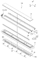
次に、下側イメージセンサユニット10Aおよび上側イメージセンサユニット10Bの構成について説明する。下側イメージセンサユニット10Aおよび上側イメージセンサユニット10Bは同一構成であるので、ここでは下側イメージセンサユニット10Aを取り上げて説明する。図2は下側イメージセンサユニット10Aの分解斜視図である。図3は図2に示す下側イメージセンサユニット10Aのうち、長手方向における一方側を拡大した斜視図である。下側イメージセンサユニット10Aは概して長方体に形成され、その長手方向が主走査方向となり、これに直交する副走査方向は紙幣Sの搬送方向Fとなる。
Next, the configuration of the lower
下側イメージセンサユニット10Aは、カバーガラス13、フレーム14、導光ユニット20、集光体38、センサ基板40、イメージセンサ45、光源部50などを備えている。これらの構成部材のうち、導光ユニット20および光源部50は照明装置として機能する。また、上述した構成部材のうち、カバーガラス13、フレーム14、導光ユニット20、センサ基板40およびイメージセンサ45は、読み取る紙幣Sの主走査方向の幅寸法に応じた長さに形成される。
カバーガラス13はフレーム14内に塵が侵入するのを防止するものである。カバーガラス13は略平板状であって、フレーム14を上側から覆うように、例えば両面テープなどを用いて固定される。なお、カバーガラス13はガラスに限られず、例えばアクリルやポリカーボネートなどの透明な樹脂材料が適用できる。
The lower
The
フレーム14は、下側イメージセンサユニット10Aの各構成部材を収容する収容部材である。フレーム14は、主走査方向に長い略直方体であり、内部には各構成部材を位置決めして支持できるように形成される。図1に示すように、フレーム14の略中央には、集光体38を収容する集光体収容部15が主走査方向に形成される。また、フレーム14には集光体収容部15を挟んだ両側に導光ユニット20を収容する導光収容部16が形成される。また、フレーム14の下面には、センサ基板40を配置するための基板収容部17が主走査方向に亘ってフレーム14の外側から凹状に形成される。フレーム14には、例えばポリカーボネートなどの樹脂材料が適用できる。
The
導光ユニット20は、長手方向の一方側の入射面および長手方向の他方側の入射面から入射された光源部50の光を原稿Sに導く。本実施形態の導光ユニット20は、第1の反射光用導光部(第1の導光部)21aと、第2の反射光用導光部(第2の導光部)21bと、透過光用導光部31とを有し、それぞれが並列に配置されている。
第1の反射光用導光部21aおよび第2の反射光用導光部21bは、図1に示す集光体38の光軸Z1を中心に線対称な略同一の構成であり、ここでは第1の反射光用導光部21aについて説明する。
The
The first reflective
図3に示すように、第1の反射光用導光部21aは導光体22と導光保持部材26とを有している。導光体22は、光源部50からの光を反射用光として紙幣Sに出射する。導光体22は、例えばアクリル系の透明な樹脂材料により形成され、主走査方向に長い棒状に形成される。導光体22は、長手方向における一方側の端部に入射面23aが形成され、他方側の端部に入射面23bが形成される。入射面23a、23bは、主走査方向に対して直交し、光源部50からの光が入射される。
As shown in FIG. 3, the first reflected
また、導光体22には、紙幣Sと対面する面に導光体22内に入射された光を紙幣Sに向かって出射させる出射面24が形成される。また、導光体22は、出射面24以外の主走査方向に沿った面が入射面23a、23bから入射された光を反射させて導光体22の長手方向に伝搬させる反射面として機能する。
In addition, the
導光保持部材26は導光体22を長手方向に亘って保持する。導光保持部材26は、主走査方向に沿って導光体22と略同一の長さに形成される。図1に示すように、導光保持部材26は、集光体38が配置される側を開口した断面略C字状に形成される。
導光保持部材26は、導光体22の出射面24の一部を上側から覆うことにより、紙幣Sに出射させる光の方向を規制する。また、導光保持部材26の内周面は、導光体22に入射された光を導光体22の出射面24側に反射させる反射面として機能する。
The light
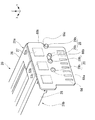
The light
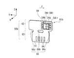
図4は、第1の反射光用導光部21aおよび第2の反射光用導光部21bの長手方向における一方側の端部の周辺を示す斜視図である。図4に示すように、導光保持部材26の長手方向における一方側の端部は、上側に板状の庇部27が一体で形成され、下側に位置合わせ部28が一体で形成される。庇部27は、導光体22の入射面23aと、光源部50との間から光源部50からの光が漏れないように遮蔽する。位置合わせ部28は、光源部50側に向かって平行に突出する、例えば複数(2つ)の円柱状の突起29aである。位置合わせ部28は、後述する第1の回路基板60aの被位置合わせ部65に接続されることで、導光保持部材26を介して導光体22と光源部50とが位置決めされる。
なお、導光保持部材26の長手方向における他方側の端部も、同様に庇部27と、位置合わせ部28としての突起29bが形成される。
FIG. 4 is a perspective view showing the periphery of one end in the longitudinal direction of the first reflected
Note that a
図3に示すように、透過光用導光部31は、導光体32と導光保持部材36とを有している。導光体32は、光源部50からの光を透過用光として紙幣Sに出射する。導光体32は、例えばアクリル系の透明な樹脂材料により形成され、主走査方向に長い棒状に形成される。導光体32は、長手方向における一方側の端部に入射面33aが形成され、他方側の端部に入射面33bが形成される。入射面33a、33bは、主走査方向に対して直交し、光源部50からの光が入射される。
As shown in FIG. 3, the transmitted
また、導光体32には、紙幣Sと対面する面に導光体32内に入射された光を紙幣Sに向かって出射させる出射面34が形成される。また、導光体32は、出射面34以外の主走査方向に沿った面が入射面33a、33bから入射された光を反射させて導光体32内の長手方向に伝搬させる反射面として機能する。
Further, the
導光保持部材36は導光体32を長手方向に亘って保持する。導光保持部材36は、主走査方向に沿って導光体32と略同一の長さに形成される。図1に示すように、導光保持部材36は、上側を開口した断面略C字状に形成される。
また、第1の反射光用導光部21aの導光体22、第2の反射光用導光部21bの導光体22および透過光用導光部31の導光体32は、フレーム14内で副走査方向に並列して配置される。
The light
Further, the
集光体38は、紙幣Sからの反射光および紙幣Sからの透過光をイメージセンサ45上に結像する光学部材である。集光体38は、例えば複数の正立等倍結像型の結像素子(ロッドレンズ)が主走査方向に直線状に配列されるロッドレンズアレイが適用できる。なお、集光体38は、イメージセンサ45上に結像できればよく、上述した構成に限定されない。集光体38には各種マイクロレンズアレイなど、従来公知の各種集光機能を有する光学部材が適用できる。
The
センサ基板40は、主走査方向に長い平板状に形成される。センサ基板40の実装面41は、上下方向に対して直交する。センサ基板40の実装面41上には、光源部50を発光させたり、イメージセンサ45を駆動させたりするための駆動回路などが実装される。また、センサ基板40の長手方向における一方側の端部には第1の回路基板60aが挿入される接続部としての接続孔42aが形成され、他方側の端部には第2の回路基板60bが挿入される接続部としての接続孔42bが形成される。接続孔42a、42bは副走査方向に長い長孔状である。
The
イメージセンサ45は、センサ基板40に実装され、集光体38の下側に配置される。イメージセンサ45は、下側イメージセンサユニット10Aの読み取りの解像度に応じた複数の光電変換素子から構成されるイメージセンサIC46の所定数を実装面41上に主走査方向に直線状に配列して実装される。イメージセンサ45は、紙幣Sからの反射光および透過光が集光体38によって結像された光を受光して電気信号に変換する。なお、イメージセンサ45は、紙幣Sからの反射光および透過光を電気信号に変換できるものであればよく、上述した構成に限定されない。イメージセンサIC46には、従来公知の各種イメージセンサICが適用できる。
The
光源部50は、光を発光することで導光ユニット20を介して紙幣Sに光を出射する。光源部50は、導光ユニット20の長手方向における一方側の端部に配置される一方側光源部51aと他方側の端部に配置される他方側光源部51bを有している。
図5Aは、一方側光源部51aの構成を示す斜視図である。一方側光源部51aは、第1の回路基板60aの同一の実装面61に実装される複数の光源52(52a、52b、52c)を有している。光源52には、表面に発光素子としてのLEDチップ54が実装される、いわゆるトップビュータイプの表面実装型のLEDパッケージが適用できる。表面実装型のLEDパッケージは汎用されているために、下側イメージセンサユニット10Aに適用することでコストを削減することができる。
複数の光源52(52a、52b、52c)は発光面を主走査方向に指向させた状態で、副走査方向(搬送方向F)に沿って並列して実装される。
The
FIG. 5A is a perspective view illustrating a configuration of the one-side
The plurality of light sources 52 (52a, 52b, 52c) are mounted in parallel along the sub-scanning direction (conveying direction F) with the light emitting surface oriented in the main scanning direction.
一方側光源部51aのうち、搬送方向Fの上流側に実装された光源は、第1の反射光用導光部21aの導光体22の入射面23aに対面して配置される第1の反射光用光源52aである。ここで、第1の反射光用光源52aは、第1の光源の一例に相当する。
第1の反射光用光源52aは、複数(例えば4つ)のLEDチップ54r、54g、54b、54irが透明樹脂によって封止された状態で配置されている。LEDチップ54r、54g、54bは可視光として、それぞれ赤、緑、青(以下、RGBともいう)の発光波長を発光する。また、LEDチップ54irは赤外光(以下、IRともいう)の発光波長を発光する。なお、赤外光などの不可視光の発光波長を発光させるのは、不可視インクによって印刷された紙幣Sの画像を読み取るためである。
The light source mounted on the upstream side in the transport direction F in the one-side
The first reflected
また、一方側光源部51aのうち、中央に実装された光源は、第2の反射光用導光部21bの導光体22の入射面23aに対面して配置される第2の反射光用光源52bである。ここで、第2の反射光用光源52bは、第4の光源の一例に相当する。
第2の反射光用光源52bは、LEDチップ54uvが透明樹脂によって封止された状態で配置されている。LEDチップ54uvは、紫外光(以下、UVともいう)の発光波長を発光する。
また、一方側光源部51aのうち、搬送方向Fの下流側に実装された光源は、透過光用導光部31の導光体32の入射面33aに対面して配置される透過光用光源52cである。透過光用光源52cは、LEDチップ54uvが透明樹脂によって封止された状態で配置されている。
In addition, the light source mounted in the center of the one-side
The second reflected
The light source mounted on the downstream side in the transport direction F in the one-side
第1の回路基板60aは、平板状に形成され、上側が複数の光源52が実装される実装部62であり、下側が上述したセンサ基板40の接続孔42aに接続される被接続部63である。実装部62の実装面61には、予め複数の光源52を所定の位置に半田付けなどによって実装される。被接続部63には、センサ基板40と電気的に接続するための複数(例えば8つ)の外部接続用パッド64が搬送方向Fに所定の間隔で形成される。なお、被接続部63には図示しない回路パターンが形成され、各光源52と外部接続用パッド64とを電気的に接続している。また、被接続部63には、被位置合わせ部65が形成される。被位置合わせ部65は、導光保持部材26の突起29aが挿入される挿入孔66a、66bと切欠き部66cとを有している。
The
一方、図5Bは、他方側光源部51bの構成を示す斜視図である。他方側光源部51bは、第2の回路基板60bの同一の実装面61に実装される複数の光源53(53a、53b、53c)を有している。他方側光源部51bは、一方側光源部51aと同様に、複数の光源53(53a、53b、53c)が発光面を主走査方向に指向させた状態で、副走査方向(搬送方向F)に沿って並列して実装される。
On the other hand, FIG. 5B is a perspective view showing a configuration of the other-side
他方側光源部51bのうち、搬送方向Fの上流側に実装された光源は、第1の反射光用導光部21aの導光体22の入射面23bに対面して配置される第1の反射光用光源53aである。ここで、第1の反射光用光源53aは、第3の光源の一例に相当する。
第1の反射光用光源53aは、LEDチップ54uvが透明樹脂によって封止された状態で配置されている。
また、他方側光源部51bのうち、中央に実装された光源は、第2の反射光用導光部21bの導光体22の入射面23bに対面して配置される第2の反射光用光源53bである。ここで、第2の反射光用光源53bは、第2の光源の一例に相当する。
第2の反射光用光源53bは、複数(例えば4つ)のLEDチップ54r、54g、54b、54irが透明樹脂によって封止された状態で配置されている。
また、他方側光源部51bのうち、搬送方向Fの下流側に実装された光源は、透過光用導光部31の導光体32の入射面33bに対面して配置される透過光用光源53cである。透過光用光源53cは、複数(例えば4つ)のLEDチップ54r、54g、54b、54irが透明樹脂によって封止された状態で配置されている。
The light source mounted on the upstream side in the transport direction F in the other
The first reflected
In addition, the light source mounted in the center of the other
The second reflected
In addition, the light source mounted on the downstream side in the transport direction F among the other-side
第2の回路基板60bは、平板状に形成され、上側が複数の光源53が実装される実装部62であり、下側が上述したセンサ基板40の接続孔42bに接続される被接続部63である。第2の回路基板60bの外形は、第1の回路基板60aの外形に対して鏡面対称である。すなわち、第2の回路基板60bの外形と第1の回路基板60aとは、図5Aに示す第1の回路基板60aの中心線Cvに対して線対称な形状であり、同一の構成は同一符号を付して、その説明を省略する。
The
したがって、第1の反射光用導光部21aの長手方向における両端部に配置される、第1の反射光用光源52aおよび第1の反射光用光源53aによって、第1の反射光用導光部21aには入射面23a、23bを介して赤、緑、青、赤外光および紫外光が入射される。
同様に、第2の反射光用導光部21bの長手方向における両端部に配置される、第2の反射光用光源52bおよび第2の反射光用光源53bによって、第2の反射光用導光部21bには入射面23a、23bを介して赤、緑、青、赤外光および紫外光が入射される。
同様に、透過光用導光部31の長手方向における両端部に配置される、透過光用光源52cおよび透過光用光源53cによって、透過光用導光部31には入射面33a、33bを介して赤、緑、青、赤外光および紫外光が入射される。
Therefore, the first light guide for reflected light is provided by the first light source for reflected light 52a and the first light source for reflected light 53a arranged at both ends in the longitudinal direction of the first light guide portion for reflected light 21a. Red, green, blue, infrared light and ultraviolet light are incident on the
Similarly, the second reflected
Similarly, the transmitted
次に、上述したように構成される画像読取部11の基本動作について説明する。画像読取部11は搬送ローラ101A、101Bおよび102A、102Bにより所定の搬送速度で搬送方向Fに搬送される紙幣Sに対し、第1の反射光用光源52a、53aおよび第2の反射光用光源52b、53bのLEDチップ54r、54g、54b、54ir、54uvをそれぞれ順次、点灯駆動させる。第1の反射光用光源52a、53aおよび第2の反射光用光源52b、53bから発光された光はそれぞれの入射面23a、23bから第1の反射光用導光部21aおよび第2の反射光用導光部21bの各導光体22内に入射する。入射した光は第1の反射光用導光部21aおよび第2の反射光用導光部21bの各導光体22の出射面24から、図1において代表的に示される矢印L1のように紙幣Sの読取位置O1を指向して反射用光として出射される。反射用光は集光体38を挟んだ2方向から紙幣Sの一方の面(下面)に対して、主走査方向に亘ってライン状に均一に照射される。
反射用光は紙幣Sによって反射されることで反射光として、集光体38を介してイメージセンサ45上に結像される。この結像された反射光は、イメージセンサ45により電気信号に変換された後、図示しない信号処理部において処理される。
Next, the basic operation of the
The reflection light is reflected by the banknote S and is imaged on the
このようにしてRGB、IR、UV全ての反射光を1走査ライン分読み取ることで、紙幣Sの主走査方向における1走査ラインの読取動作を完了する。1走査ラインの読取動作終了後、紙幣Sの副走査方向への移動に伴い、上述と同様に次の1走査ライン分の読取動作が行われる。このように紙幣Sを搬送方向Fに搬送しながら1走査ライン分ずつ読取動作を繰り返すことで、紙幣Sの全面が順次走査されて反射光による画像情報の読み取りが実施される。
なお、上側イメージセンサユニット10Bの画像読取部11についても他方の面(上面)に対して同様に実施される。
In this way, the reading operation of one scanning line in the main scanning direction of the banknote S is completed by reading all reflected light of RGB, IR, and UV for one scanning line. After the reading operation for one scanning line is completed, the reading operation for the next one scanning line is performed in the same manner as described above as the bill S moves in the sub-scanning direction. Thus, by repeating the reading operation for each scanning line while transporting the banknote S in the transport direction F, the entire surface of the banknote S is sequentially scanned, and image information is read by reflected light.
Note that the
次に、上述したように構成される透過光用照明部12の動作について説明する。透過光用照明部12は、搬送ローラ101A、101Bおよび102A、102Bにより所定の搬送速度で搬送方向Fに搬送される紙幣Sに対し、透過光用光源52c、53cのLEDチップ54r、54g、54b、54ir、54uvを順次、点灯駆動させる。透過光用光源52c、53cから発光された光はそれぞれの入射面33a、33bから透過光用導光部31内に入射する。入射した光は透過光用導光部31の出射面34から、図1において代表される矢印L2のように紙幣Sの読取位置O2を指向して透過用光として出射される。透過用光は紙幣Sの一方の面(下面)に対して、主走査方向に亘ってライン状に均一に照射される。
透過用光は紙幣Sを透過することで透過光として、上側イメージセンサユニット10Bの集光体38を介してイメージセンサ45上に結像される。この結像された透過光は、上側イメージセンサユニット10Bのイメージセンサ45より電気信号に変換された後、図示しない信号処理部において処理される。
Next, the operation of the transmitted
The light for transmission passes through the banknote S, and forms an image on the
このようにしてRGB、IR、UV全ての透過光を1走査ライン分読み取ることで、紙幣Sの主走査方向における1走査ラインの読取動作を完了する。1走査ラインの読取動作終了後、紙幣Sの副走査方向への移動に伴い、上述と同様に次の1走査ライン分の読取動作が行われる。このように紙幣Sを搬送方向Fに搬送しながら1走査ライン分ずつ読取動作を繰り返すことで、紙幣Sの全面が順次走査されて透過光による画像情報の読み取りが実施される。
なお、上側イメージセンサユニット10Bの透過光用照明部12についても他方の面(上面)に対して同様に実施される。
In this way, the reading operation of one scanning line in the main scanning direction of the banknote S is completed by reading all transmitted light of RGB, IR, and UV for one scanning line. After the reading operation for one scanning line is completed, the reading operation for the next one scanning line is performed in the same manner as described above as the bill S moves in the sub-scanning direction. In this way, by repeating the reading operation for each scanning line while transporting the banknote S in the transport direction F, the entire surface of the banknote S is sequentially scanned, and image information is read by transmitted light.
The transmitted
次に、上述したように構成されるイメージセンサユニット部10の組み立て方法について説明する。下側イメージセンサユニット10Aおよび上側イメージセンサユニット10Bは略同一の構成であり、ここでは下側イメージセンサユニット10Aについて説明する。
ここで、本実施形態では、寸法精度や熱源の位置によって、第1の反射光用導光部21aおよび第2の反射光用導光部21bが異なる長さに伸縮した場合でも、第1の回路基板60aおよび第2の回路基板60bが傾斜しないような組み立て方法を採用している。
まず、下側イメージセンサユニット10Aを構成する構成部材を用意する。このとき、第1の回路基板60aおよび第2の回路基板60bには、予め図5Aおよび図5Bに示すように複数の光源52、53を所定の位置に実装する。また、センサ基板40には、予めイメージセンサ45、駆動回路などを所定の位置に実装する。
Next, a method for assembling the
Here, in this embodiment, even when the first reflected
First, constituent members constituting the lower
次に、導光体22を導光保持部材26に保持させて、第1の反射光用導光部21aおよび第2の反射光用導光部21bを構成する。同様に、導光体32を導光保持部材36に保持させて、透過光用導光部31を構成する。
次に、図4に示すように、第1の反射光用導光部21aと第2の反射光用導光部21bとを互いに対面させた状態で維持する。この状態から、各導光保持部材26の長手方向における一方側に形成された位置合わせ部28と、第1の回路基板60aの被位置合わせ部65とを接続させることで位置決めする。具体的には、各位置合わせ部28の突起29aを挿入孔66a、66b、切欠き部66cに挿入する。なお、挿入孔66bには、2つの突起29aが挿入される。
Next, the
Next, as shown in FIG. 4, the first reflected
したがって、第1の反射光用光源52aが第1の反射光用導光部21aの導光体22の入射面23aに精度よく対面し、第2の反射光用光源52bが第2の反射光用導光部21bの導光体22の入射面23aに精度よく対面する。
Therefore, the first reflected
ここで、本実施形態では、第1の回路基板60aは、第1の反射光用導光部21aに対して結合され、第2の反射光用導光部21bに対して主走査方向に沿ってスライド可能に接続される。
図6は、導光ユニット20と第1の回路基板60aとが接続される状態を示す斜視図である。ここでは、第1の反射光用導光部21aの一方側の各突起29aは、それぞれ挿入孔66bおよび切欠き部66cに挿入された後に先端をかしめることで、第1の反射光用導光部21aと第1の回路基板60aとを結合する。かしめには突起29aの先端を熱で溶融させる熱かしめを用いることができる。第1の反射光用導光部21aの一方側の各突起29aは、第1の回路基板60aと結合される結合突起の一例に相当する。
一方、第2の反射光用導光部21bの一方側の各突起29aは、それぞれ挿入孔66aおよび挿入孔66bに挿入したままにする。したがって、第1の回路基板60aは、第2の反射光用導光部21bの長手方向に沿ってスライド可能に接続される。第2の反射光用導光部21bの一方側の突起29aは、第1の回路基板60aを主走査方向にスライド可能に案内する案内突起の一例に相当する。
Here, in the present embodiment, the
FIG. 6 is a perspective view showing a state where the
On the other hand, the
同様に、各導光保持部材26の長手方向における他方側に形成された位置合わせ部28と、第2の回路基板60bの被位置合わせ部65とを接続させることで位置決めする。
したがって、第1の反射光用光源53aが第1の反射光用導光部21aの入射面23bに精度よく対面し、第2の反射光用光源53bが第2の反射光用導光部21bの入射面23bに精度よく対面する。
Similarly, the positioning is performed by connecting the
Therefore, the first reflected
本実施形態では、第2の回路基板60bは、第1の反射光用導光部21aに対して主走査方向に沿ってスライド可能に接続され、第2の反射光用導光部21bに対して結合される。
図7は、導光ユニット20と第2の回路基板60bとを接続した状態を示す斜視図である。ここでは、第1の反射光用導光部21aの他方側の各突起29bは、それぞれ挿入孔66bおよび切欠き部66cに挿入したままにする。したがって、第2の回路基板60bは、第1の反射光用導光部21aの長手方向に沿ってスライド可能に接続される。第1の反射光用導光部21aの他方側の突起29bは、第2の回路基板60bを主走査方向にスライド可能に案内する案内突起の一例に相当する。
一方、第2の反射光用導光部21bの他方側の各突起29bは、それぞれ挿入孔66aおよび挿入孔66bに挿入された後に先端をかしめることで、第2の反射光用導光部21bと第2の回路基板60bとを結合する。かしめには突起29bの先端を熱で溶融させる熱かしめを用いることができる。第2の反射光用導光部21bの他方側の各突起29bは、第2の回路基板60bと結合される結合突起の一例に相当する。
In the present embodiment, the
FIG. 7 is a perspective view showing a state in which the
On the other hand, each
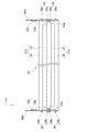
図8は、導光ユニット20と、第1の回路基板60aおよび第2の回路基板60bとを接続した状態を上側から見た平面図である。
図8に示すように、第1の反射光用導光部21aは、一方側が第1の回路基板60aにかしめられることで結合され、他方側が第2の回路基板60bに対してかしめられていないことから相対的にスライド可能である。また、第2の反射光用導光部21bは、一方側が第1の回路基板60aに対してかしめられていないことから相対的にスライド可能であり、他方側が第2の回路基板60bに対してかしめられることで結合される。
FIG. 8 is a plan view of a state in which the
As shown in FIG. 8, the first reflected
次に、集光体38をフレーム14の上側から集光体収容部15に収容する。更に、第1の回路基板60aおよび第2の回路基板60bが接続された、第1の反射光用導光部21aおよび第2の反射光用導光部21bをフレーム14の上側から導光収容部16に収容する。同様に、透過光用導光部31をフレーム14の上側から導光収容部16に収容する。その後、カバーガラス13をフレーム14の上側から覆うように、フレーム14の上面に固定する。
Next, the
次に、カバーガラス13が下面になるようにフレーム14を上下反転させた後、上下反転させたセンサ基板40を基板収容部17に収容する。このとき、センサ基板40の長手方向における一方側に形成された接続孔42aにフレーム14から突出されている第1の回路基板60aの被接続部63を挿入する。また、センサ基板40の長手方向における他方側に形成された接続孔42bにフレーム14から突出されている第2の回路基板60bの被接続部63を挿入する。したがって、第1の回路基板60aおよび第2の回路基板60bがセンサ基板40の長手方向の端部に接続される。
Next, the
その後、接続孔42a、42bからセンサ基板40の下面から露出された第1の回路基板60a、第2の回路基板60bの外部接続用パッド64を、センサ基板40にそれぞれ半田付けする。次に、基板収容部17に収容されたセンサ基板40を、例えば熱かしめにより基板収容部17内に固定することで、下側イメージセンサユニット10Aが製造される。
Thereafter, the
このように、本実施形態の第1の反射光用導光部21aは、長手方向の一方側の入射面23aに第1の反射光用光源52aが対面して配置され、第1の回路基板60aを結合すると共に第2の回路基板60bを第1の反射光用導光部21aの長手方向に沿ってスライド可能に接続する。一方、第2の反射光用導光部21bは、長手方向の他方側の入射面23bに第2の反射光用光源53bが対面して配置され、第2の回路基板60bを結合すると共に第1の回路基板60aを第1の反射光用導光部21bの長手方向に沿ってスライド可能に接続する。
As described above, in the first reflected
ここで、熱源からの位置により、例えば第1の反射光用導光部21aが第2の反射光用導光部21bよりも伸長した場合を想定する。仮に、第2の反射光用導光部21bが第1の回路基板60aと第2の回路基板60bとの両方に結合されていると、第1の回路基板60aおよび第2の回路基板60bは第2の反射光用導光部21bの伸縮に追随して中心に向かって引っ張られ副走査方向に対して傾斜してしまう。本実施形態では、第1の回路基板60aが第2の反射光用導光部21bに対して追随せず、第2の反射光用導光部21bと第1の回路基板60aとが伸縮方向に相対的にスライドする。したがって、第1の回路基板60aおよび第2の回路基板60bが中心に向かって引っ張られることがないため、第1の回路基板60aおよび第2の回路基板60bの傾斜を防止することができる。したがって、第1の回路基板60aおよび第2の回路基板60bに実装された各光源52、53の傾斜も防止することができるので、各光源52、53から第1の反射光用導光部21aおよび第2の反射光用導光部21bに入射される光量が低下することを防止することができる。
また、ここでは、第1の反射光用導光部21aが第2の反射光用導光部21bよりも伸長した場合を想定したが、第2の反射光用導光部21bが第1の反射光用導光部21aよりも伸長した場合でも各光源52、53から入射される光量が低下することを防止することができる。
Here, it is assumed that, for example, the first reflected
In addition, here, it is assumed that the first reflected
なお、上述した実施形態に限られず、第1の反射光用導光部21aまたは第2の反射光用導光部21bは一方側で第1の回路基板60aに結合されている場合、他方側で第2の回路基板60bとスライド可能に接続されていればよい。あるいは、第1の反射光用導光部21aまたは第2の反射光用導光部21bは一方側で第1の回路基板60aにスライド可能に接続されている場合、他方側で第2の回路基板60bに結合されていればよい。
The first reflected
ここで、本実施形態の変形例について図9を参照して説明する。
図9は、導光ユニット20と、第1の回路基板60aおよび第2の回路基板60bとを接続した状態を上側から見た平面図である。図8と異なり、第2の反射光用導光部21aは、一方側が第1の回路基板60aにかしめられることで結合され、他方側が第2の回路基板60bに対してかしめられていないことからスライド可能である。
すなわち、第1の回路基板60aは第1の反射光用導光部21aおよび第2の反射光用導光部21bの何れにも結合され、第2の回路基板60bは第1の反射光用導光部21aおよび第2の反射光用導光部21bの何れにもスライド可能である。
このように、各反射光用導光部において、第1の回路基板60aおよび第2の回路基板60bの何れか一方に結合され、他方にスライド可能であればよい。
Here, a modification of the present embodiment will be described with reference to FIG.
FIG. 9 is a plan view of a state in which the
That is, the
As described above, in each reflected light guide unit, it is only necessary to be coupled to one of the
(第2の実施形態)
第2の実施形態では、第1の回路基板82aおよび第2の回路基板82bが単数の光源を実装すると共に、透過光用導光部31を省略する場合について説明する。なお、第1の実施形態と同様の構成は同一符号を付して、その説明を省略する。
図10は、第2の実施形態のイメージセンサユニット80を示す断面図である。ここでは、透過光を読み取る必要がないので、紙幣Sの上側には上側イメージセンサユニットが配置されない。図10に示すようにイメージセンサユニット80は、第1の実施形態の透過光用導光部31を省略した構成である。すなわち、イメージセンサユニット80は、第1の反射光用導光部21aと、第2の反射光用導光部21bとの2つの導光部を有している。
(Second Embodiment)
In the second embodiment, a case will be described in which the
FIG. 10 is a sectional view showing the
図11Aは、第1の反射光用導光部21aおよび第2の反射光用導光部21bの長手方向における一方側の端部に配置され、第1の回路基板82aに実装される一方側光源部81aを示す斜視図である。図11Aに示すように、第1の回路基板82aには、実装面61に、光源83のみが実装される。光源83は第1の反射光用導光部21aの入射面23aに対面する。
FIG. 11A shows one side mounted on the
図11Bは、第1の反射光用導光部21aおよび第2の反射光用導光部21bの長手方向における他方側の端部に配置され、第2の回路基板82bに実装される他方側光源部81bを示す斜視図である。図11Bに示すように、第2の回路基板82bには、実装面61に、光源84のみが実装される。光源84は第2の反射光用導光部21aの入射面23bに対面する。
FIG. 11B shows the other side mounted on the
図12は、導光ユニット20と、第1の回路基板82aおよび第2の回路基板82bとを接続した状態を上側から見た平面図である。
図12に示すように、第1の反射光用導光部21aは、一方側が第1の回路基板82aにかしめられることで結合され、他方側が第2の回路基板82bに対してかしめられていないことから相対的にスライド可能である。また、第2の反射光用導光部21bは、一方側が第1の回路基板82aに対してかしめられていないことから相対的にスライド可能であり、他方側が第2の回路基板82bに対してかしめられることで結合される。
FIG. 12 is a plan view of the state in which the
As shown in FIG. 12, the first reflected
したがって、本実施形態でも第1の実施形態と同様に、第1の反射光用導光部21aおよび第2の反射光用導光部21bがそれぞれ伸縮して長さが異なった場合でも、第1の回路基板82aおよび第2の回路基板82bが副走査方向に対して傾斜することを防止される。したがって、第1の回路基板82aおよび第2の回路基板82bに実装された各光源83、84から第1の反射光用導光部21aおよび第2の反射光用導光部21bに入射される光量が低下することを防止することができる。
Therefore, even in the present embodiment, as in the first embodiment, even when the first reflected
なお、本実施形態のように、第1の回路基板82aに光源83のみが実装される場合、光源83と光源83が対面する第1の反射光用導光部21aとの間に隙間が生じないように、第1の反射光用導光部21aと第1の回路基板82aとを結合することが好ましい。同様に、第2の回路基板82bに光源84のみが実装される場合、光源84と光源84が対面する第2の反射光用導光部21bとの間に隙間が生じないように、第2の反射光用導光部21bと第2の回路基板82bとを結合することが好ましい。
When only the
以上、本発明の好ましい実施形態について説明したが、本発明はこれらの実施形態に限定されず、その要旨の範囲内で種々の変形および変更が可能である。
上述した各実施形態では、2つの導光部(第1の反射光用導光部21a、第2の反射光用導光部21b)を第1の回路基板60a、82aおよび第2の回路基板60b、82bに接続する場合について説明したが、この場合に限られない。3つ以上の導光部を第1の回路基板60aおよび第2の回路基板60bに接続してもよい。この場合、追加した導光部も、第1の回路基板60aおよび第2の回路基板60bの何れか一方を結合し、他方をスライド可能に接続する。
As mentioned above, although preferable embodiment of this invention was described, this invention is not limited to these embodiment, A various deformation | transformation and change are possible within the range of the summary.
In each of the above-described embodiments, the two light guides (the first reflected
また、第1の実施形態では、第1の反射光用導光部21aの長手方向における一方側にRGB、IRを発光する第1の反射光用光源52aを配置し、他方側にUVを発光する第1の反射光用光源53aを配置した。また、第2の反射光用導光部21bの長手方向における一方側にUVを発光する第2の反射光用光源52bを配置し、他方側にRGB、IRを発光する第2の反射光用光源53bを配置する場合について説明した。しかしながら、仕様に応じた発光波長の光(ここでは、RGB、IR、UV)を第1の反射光用導光部21aまたは第2の反射光用導光部21bを介して紙幣Sに出射できればよく、上述した配置に限定されない。同様に、第2の実施形態でも、第1の反射光用導光部21aまたは第2の反射光用導光部21bは、上述した光源83、84に限定されない。
また、IR、UVを出射させる必要がない場合には、IR、UVを発光させる発光素子を除外した光源や、IR、UVを発光させる発光素子をRGBを発光させる発光素子に替えた光源を用いることができる。
In the first embodiment, the first reflected
When there is no need to emit IR and UV, a light source that excludes light emitting elements that emit IR and UV, or a light source that replaces light emitting elements that emit IR and UV with light emitting elements that emit RGB light is used. be able to.
また、上述した第1の実施形態では、下側イメージセンサユニット10Aおよび上側イメージセンサユニット10Bは、図1に示す中心線Ocに対して対称な同一構成である場合について説明したが、この場合に限られない。すなわち、下側イメージセンサユニット10Aおよび上側イメージセンサユニット10Bは、同一構成でなくてもよい。例えば、透過光用照明部12は片側のみ有していてもよい。
In the first embodiment described above, the case where the lower
また、第1の反射光用導光部21aおよび第2の反射光用導光部21bは、導光体22と、導光保持部材26とを有する場合について説明したが、この場合に限られず、導光体22のみで構成してもよい。この場合には、導光体22自体に、位置決め部28を形成することができる。
また、各反射光用導光部と回路基板とは熱かしめで結合する場合に限られず、接着剤で固定する場合など、他の方法で結合されていてもよい。
Moreover, although the case where the first reflected
Further, each light guide for reflected light and the circuit board are not limited to the case of being joined by heat caulking, and may be joined by other methods such as fixing with an adhesive.
10:イメージセンサユニット部 10A:下側イメージセンサユニット 10B:上側イメージセンサユニット 14:フレーム 21a:第1の反射光用導光部 21b:第2の反射光用導光部 22:導光体 23a、23b:入射面 26:導光保持部材 29a、29b:突起 31:透過光用導光部 32:導光体 33a、33b:入射面 36:導光保持部材 38:集光体 40:センサ基板 45:イメージセンサ 51a:一方側光源部 51b:他方側光源部 52a、52b:第1の反射用光源 53a、53b:第2の反射用光源 52c、53c:透過光用光源 60a:第1の回路基板 60b:第2の回路基板 61:実装面 63:被接続部 66a、66b:挿入孔 66c:切欠き部 80:イメージセンサユニット 81a:一方側光源部 81b:他方側光源部 82a:第1の回路基板 82b:第2の回路基板 83:光源 84:光源 101A、101B、102A、102B:搬送ローラ(移送部) 103:比較部 104:記憶部 100:画像読取装置(紙葉類識別装置)
10:
Claims (14)
第2の光源と、
前記第1の光源を実装する第1の回路基板と、
前記第2の光源を実装する第2の回路基板と、
長手方向の一方側に前記第1の回路基板が配置され、長手方向の他方側に前記第2の回路基板が配置され、前記第1の光源および前記第2の光源からの光を被照明体に導く導光ユニットと、を有する照明装置であって、
前記導光ユニットは、
並列して配置される、第1の導光部と、第2の導光部と、を有し、
前記第1の導光部は、長手方向の一方側の入射面に前記第1の光源が対面して配置され、前記第1の回路基板を結合すると共に前記第2の回路基板を前記第1の導光部の長手方向に沿ってスライド可能に接続し、
前記第2の導光部は、長手方向の他方側の入射面に前記第2の光源が対面して配置され、前記第1の回路基板および前記第2の回路基板のうち一方を結合すると共に他方を前記第2の導光部の長手方向に沿ってスライド可能に接続することを特徴とする照明装置。 A first light source;
A second light source;
A first circuit board on which the first light source is mounted;
A second circuit board on which the second light source is mounted;
The first circuit board is disposed on one side in the longitudinal direction, the second circuit board is disposed on the other side in the longitudinal direction, and the light from the first light source and the second light source is illuminated. A light guide unit that leads to a lighting device,
The light guide unit is:
Having a first light guide part and a second light guide part arranged in parallel;
The first light guide unit is disposed so that the first light source faces an incident surface on one side in a longitudinal direction, and the first circuit board is coupled to the first circuit board and the second circuit board is disposed to the first light guide unit. Slidably connected along the longitudinal direction of the light guide,
The second light guide unit is disposed with the second light source facing the incident surface on the other side in the longitudinal direction, and couples one of the first circuit board and the second circuit board. The other is slidably connected along the longitudinal direction of the second light guide.
棒状であって、前記入射面および前記入射面から入射された光を前記被照明体に向かって出射する出射面が形成された導光体と、
前記導光体を長手方向に亘って保持する導光保持部材と、を有することを特徴とする請求項1に記載の照明装置。 Each of the first light guide and the second light guide is
A light guide having a rod-like shape and formed with an exit surface for emitting the light incident from the entrance surface and the entrance surface toward the illuminated body;
The lighting device according to claim 1, further comprising: a light guide holding member that holds the light guide body in a longitudinal direction.
前記第2の回路基板は、前記案内突起が挿入される挿入孔を有し、
前記案内突起を前記挿入孔に挿入することで前記第2の回路基板が前記第1の導光部の長手方向に沿ってスライド可能に接続されることを特徴とする請求項1または2に記載の照明装置。 The first light guide unit has a guide projection that protrudes in parallel with the longitudinal direction of the first light guide unit on the other side in the longitudinal direction.
The second circuit board has an insertion hole into which the guide protrusion is inserted,
The said 2nd circuit board is slidably connected along the longitudinal direction of the said 1st light guide part by inserting the said guide protrusion in the said insertion hole, The Claim 1 or 2 characterized by the above-mentioned. Lighting equipment.
前記第1の回路基板は、前記結合突起が挿入される挿入孔を有し、
前記結合突起を前記挿入孔に挿入し、前記結合突起の先端をかしめることで、または、接着剤で固定されることで、前記第1の回路基板が前記第1の導光部に結合されることを特徴とする請求項1ないし3の何れか1項に記載の照明装置。 The first light guide has a coupling protrusion parallel to the longitudinal direction of the first light guide on one side in the longitudinal direction,
The first circuit board has an insertion hole into which the coupling protrusion is inserted,
The first circuit board is coupled to the first light guide unit by inserting the coupling projection into the insertion hole and caulking the tip of the coupling projection or by fixing with an adhesive. The illumination device according to claim 1, wherein the illumination device is a light source.
前記第1の回路基板および前記第2の回路基板のうち前記他方は、前記案内突起が挿入される挿入孔を有し、
前記案内突起を前記挿入孔に挿入することで前記他方が前記第2の導光部の長手方向に沿ってスライド可能に接続されることを特徴とする請求項1ないし4の何れか1項に記載の照明装置。 The second light guide part has a guide projection parallel to the longitudinal direction of the second light guide part on one side or the other side in the longitudinal direction,
The other of the first circuit board and the second circuit board has an insertion hole into which the guide protrusion is inserted,
The said other side is slidably connected along the longitudinal direction of a said 2nd light guide part by inserting the said guide protrusion in the said insertion hole, The any one of Claim 1 thru | or 4 characterized by the above-mentioned. The lighting device described.
前記第1の回路基板および前記第2の回路基板のうち前記一方は、前記結合突起が挿入される挿入孔を有し、
前記結合突起を前記挿入孔に挿入し、前記結合突起の先端をかしめることで、または、接着剤で固定されることで、前記一方が前記第2の導光部に結合されることを特徴とする請求項1ないし5の何れか1項に記載の照明装置。 The second light guide part has a coupling protrusion parallel to the longitudinal direction of the second light guide part on one side or the other side in the longitudinal direction,
The one of the first circuit board and the second circuit board has an insertion hole into which the coupling protrusion is inserted,
The one is coupled to the second light guide unit by inserting the coupling projection into the insertion hole and caulking the tip of the coupling projection or by fixing with an adhesive. The illumination device according to any one of claims 1 to 5.
前記第2の回路基板は、前記第2の光源と第3の光源が実装され、
前記第1の導光部は、長手方向の両端に前記入射面を有し、長手方向の一方側の前記入射面に前記第1の光源が対面して配置され、長手方向の他方側の前記入射面に前記第3の光源が対面して配置され、
前記第2の導光部は、長手方向の両端に前記入射面を有し、長手方向の他方側の前記入射面に前記第2の光源が対面して配置され、長手方向の一方側の前記入射面に前記第4の光源が対面して配置される
ことを特徴とする請求項1ないし6の何れか1項に記載の照明装置。 The first circuit board is mounted with the first light source and the fourth light source,
The second circuit board is mounted with the second light source and the third light source,
The first light guide unit has the incident surfaces at both ends in the longitudinal direction, the first light source is arranged to face the incident surface on one side in the longitudinal direction, and the first light guide unit on the other side in the longitudinal direction. The third light source is disposed facing the incident surface,
The second light guide unit has the incident surfaces at both ends in the longitudinal direction, the second light source is disposed to face the incident surface on the other side in the longitudinal direction, and the second light source is disposed on the one side in the longitudinal direction. The lighting device according to any one of claims 1 to 6, wherein the fourth light source is arranged to face the incident surface.
第2の光源と、
第3の光源と、
第4の光源と、
前記第1の光源と第4の光源とを実装する第1の回路基板と、
前記第2の光源と第3の光源とを実装する第2の回路基板と、
長手方向の一方側に前記第1の回路基板が配置され、長手方向の他方側に前記第2の回路基板が配置され、前記第1の光源、前記第2の光源、前記第3の光源、および前記第4の光源からの光を被照明体に導く導光ユニットと、を有する照明装置であって、
前記導光ユニットは、
並列して配置される、第1の導光部と、第2の導光部と、を有し、
前記第1の導光部および前記第2の導光部はそれぞれ、棒状であって、入射面から入射された光を前記被照明体に向かって出射する出射面が形成された導光体と、前記導光体を長手方向に亘って保持する導光保持部材と、を有し、かつ、長手方向の一方側の入射面に前記第1の光源が対面して配置され、前記第1の回路基板を結合すると共に前記第2の回路基板を前記第1の導光部の長手方向に沿ってスライド可能に接続する
ことを特徴とする照明装置。 A first light source;
A second light source;
A third light source;
A fourth light source;
A first circuit board on which the first light source and the fourth light source are mounted;
A second circuit board for mounting the second light source and the third light source;
The first circuit board is disposed on one side in the longitudinal direction, the second circuit board is disposed on the other side in the longitudinal direction, and the first light source, the second light source, the third light source, And a light guide unit that guides light from the fourth light source to the body to be illuminated,
The light guide unit is:
Having a first light guide part and a second light guide part arranged in parallel;
The first light guide part and the second light guide part each have a rod shape, and a light guide body formed with an exit surface that emits light incident from the entrance surface toward the illuminated body; A light guide holding member that holds the light guide body in the longitudinal direction, and the first light source is disposed to face the incident surface on one side in the longitudinal direction, and the first light source A lighting device, wherein a circuit board is coupled and the second circuit board is slidably connected along a longitudinal direction of the first light guide.
前記第2の回路基板は、前記案内突起が挿入される挿入孔を有し、
前記案内突起を前記挿入孔に挿入することで前記第2の回路基板が長手方向に沿ってスライド可能に接続されることを特徴とする請求項8に記載の照明装置。 Each of the first light guide part and the second light guide part has a guide protrusion that protrudes in parallel to the longitudinal direction on the other side in the longitudinal direction,
The second circuit board has an insertion hole into which the guide protrusion is inserted,
The lighting device according to claim 8, wherein the second circuit board is slidably connected along a longitudinal direction by inserting the guide protrusion into the insertion hole.
前記第1の回路基板は、前記結合突起が挿入される挿入孔を有し、
前記結合突起を前記挿入孔に挿入し、前記結合突起の先端をかしめることで、または、接着剤で固定されることで、前記第1の回路基板が前記第1の導光部および前記第2の導光部に結合されることを特徴とする請求項8または9に記載の照明装置。 Each of the first light guide part and the second light guide part has a coupling protrusion parallel to the longitudinal direction on one side in the longitudinal direction,
The first circuit board has an insertion hole into which the coupling protrusion is inserted,
By inserting the coupling protrusion into the insertion hole and caulking the tip of the coupling protrusion, or by fixing with an adhesive, the first circuit board is connected to the first light guide unit and the first The illumination device according to claim 8, wherein the illumination device is coupled to the two light guide units.
前記第2の光源と前記第3の光源のうち、一方が紫外光の発光波長を発光し、他方が紫外光を含まない発光波長を発光する
ことを特徴とする請求項7ないし10の何れか1項に記載の照明装置。 One of the first light source and the fourth light source emits an emission wavelength of ultraviolet light, and the other emits an emission wavelength not containing ultraviolet light,
One of the second light source and the third light source emits an emission wavelength of ultraviolet light, and the other emits an emission wavelength not containing ultraviolet light. The lighting device according to item 1.
前記被照明体からの光を電気信号へと変換するイメージセンサと、
前記イメージセンサを実装するセンサ基板と、
を有することを特徴とするイメージセンサユニット。 The lighting device according to any one of claims 1 to 11,
An image sensor that converts light from the illuminated body into an electrical signal;
A sensor substrate on which the image sensor is mounted;
An image sensor unit comprising:
前記イメージセンサユニットと前記被照明体とを相対的に移送させる移送部と、
を有することを特徴とする画像読取装置。 An image sensor unit according to claim 12,
A transfer unit that relatively transfers the image sensor unit and the object to be illuminated;
An image reading apparatus comprising:
前記被照明体としての紙葉類を移送させる移送部と、
前記紙葉類を識別する基準となる基準データを記憶する記憶部と、
前記イメージセンサユニットに読み取られた画像情報と、前記記憶部に記憶されている前記基準データとを比較して前記紙葉類を識別する比較部と、
を有することを特徴とする紙葉類識別装置。 An image sensor unit according to claim 12,
A transfer unit for transferring paper sheets as the object to be illuminated;
A storage unit for storing reference data serving as a reference for identifying the paper sheet;
A comparison unit that compares the image information read by the image sensor unit with the reference data stored in the storage unit to identify the paper sheet;
A paper sheet identification device comprising:
Priority Applications (2)
| Application Number | Priority Date | Filing Date | Title |
|---|---|---|---|
| JP2014233733A JP2016100633A (en) | 2014-11-18 | 2014-11-18 | Illumination apparatus, image sensor unit, image reading apparatus, and paper sheet identification apparatus |
| PCT/JP2015/082314 WO2016080412A1 (en) | 2014-11-18 | 2015-11-17 | Illumination device, image sensor unit, image reading device, and paper sheet identification device |
Applications Claiming Priority (1)
| Application Number | Priority Date | Filing Date | Title |
|---|---|---|---|
| JP2014233733A JP2016100633A (en) | 2014-11-18 | 2014-11-18 | Illumination apparatus, image sensor unit, image reading apparatus, and paper sheet identification apparatus |
Publications (1)
| Publication Number | Publication Date |
|---|---|
| JP2016100633A true JP2016100633A (en) | 2016-05-30 |
Family
ID=56013947
Family Applications (1)
| Application Number | Title | Priority Date | Filing Date |
|---|---|---|---|
| JP2014233733A Pending JP2016100633A (en) | 2014-11-18 | 2014-11-18 | Illumination apparatus, image sensor unit, image reading apparatus, and paper sheet identification apparatus |
Country Status (2)
| Country | Link |
|---|---|
| JP (1) | JP2016100633A (en) |
| WO (1) | WO2016080412A1 (en) |
Families Citing this family (1)
| Publication number | Priority date | Publication date | Assignee | Title |
|---|---|---|---|---|
| US11233917B2 (en) * | 2018-07-05 | 2022-01-25 | Mitsubishi Electric Corporation | Lighting device and image reading device |
Family Cites Families (4)
| Publication number | Priority date | Publication date | Assignee | Title |
|---|---|---|---|---|
| JPH10247412A (en) * | 1997-03-03 | 1998-09-14 | Omron Corp | Surface light source device |
| JP6291707B2 (en) * | 2012-08-10 | 2018-03-14 | 三菱電機株式会社 | Contact image sensor, output correction device for contact image sensor, and output correction method for contact image sensor |
| JP5989475B2 (en) * | 2012-09-19 | 2016-09-07 | 株式会社東芝 | Image reading apparatus and paper sheet processing apparatus |
| JP5879293B2 (en) * | 2013-03-28 | 2016-03-08 | 京セラドキュメントソリューションズ株式会社 | Illumination device, and image reading apparatus and image forming apparatus provided with the same |
-
2014
- 2014-11-18 JP JP2014233733A patent/JP2016100633A/en active Pending
-
2015
- 2015-11-17 WO PCT/JP2015/082314 patent/WO2016080412A1/en active Application Filing
Also Published As
| Publication number | Publication date |
|---|---|
| WO2016080412A1 (en) | 2016-05-26 |
Similar Documents
| Publication | Publication Date | Title |
|---|---|---|
| JP5897090B2 (en) | Image sensor unit, image reading device, and paper sheet identification device | |
| JP5384707B2 (en) | Image sensor unit and image reading apparatus using the same | |
| WO2014087614A1 (en) | Image read-in device | |
| WO2013022060A1 (en) | Image sensor unit and image reading device utilizing same | |
| US9838559B2 (en) | Illumination apparatus, image sensor unit and image reading apparatus | |
| JP2015073264A (en) | Illumination device, image sensor unit, image reading device and image formation device | |
| JP5943139B2 (en) | Light guide and image reading apparatus | |
| US9363406B2 (en) | Illumination apparatus and paper sheet distinguishing apparatus | |
| JP6207359B2 (en) | Illumination device, image sensor unit, and paper sheet identification device | |
| WO2016080412A1 (en) | Illumination device, image sensor unit, image reading device, and paper sheet identification device | |
| JP2014068338A (en) | Luminaire, image sensor unit and paper sheet identification device | |
| JP2016005130A (en) | Image sensor unit, image reading device, and paper sheet identification device | |
| US11765298B2 (en) | Image sensor unit | |
| JP5897087B2 (en) | Cover member, method for manufacturing cover member, image sensor unit, image reading device, and paper sheet identification device | |
| JP6594562B2 (en) | Image reading device | |
| CN112352416B (en) | Illumination device and image reading apparatus | |
| JP2010045565A (en) | Image sensor module | |
| JP2016082248A (en) | Image sensor unit, image reading device, paper sheet identification device, and method of manufacturing image sensor unit | |
| JP2016127540A (en) | Image sensor unit, image reading apparatus, and paper sheet identification apparatus | |
| JPWO2016194493A1 (en) | Image sensor unit, paper sheet identification device, image reading device | |
| JP5917579B2 (en) | Image sensor unit and image reading apparatus | |
| JPWO2020174855A1 (en) | Lighting device and image reader | |
| JP2017225083A (en) | Image sensor unit, paper identification device, image reading device, and image forming apparatus | |
| JP2017192125A (en) | Method of manufacturing sensor unit and reading device | |
| JP2008135903A (en) | Image reader |