JP2016059043A - Antenna assembly and electronic device comprising antenna assembly - Google Patents
Antenna assembly and electronic device comprising antenna assembly Download PDFInfo
- Publication number
- JP2016059043A JP2016059043A JP2015174318A JP2015174318A JP2016059043A JP 2016059043 A JP2016059043 A JP 2016059043A JP 2015174318 A JP2015174318 A JP 2015174318A JP 2015174318 A JP2015174318 A JP 2015174318A JP 2016059043 A JP2016059043 A JP 2016059043A
- Authority
- JP
- Japan
- Prior art keywords
- antenna assembly
- ground
- radiating
- circuit board
- signal
- Prior art date
- Legal status (The legal status is an assumption and is not a legal conclusion. Google has not performed a legal analysis and makes no representation as to the accuracy of the status listed.)
- Withdrawn
Links
Images


Classifications
-
- H—ELECTRICITY
- H01—ELECTRIC ELEMENTS
- H01Q—ANTENNAS, i.e. RADIO AERIALS
- H01Q1/00—Details of, or arrangements associated with, antennas
- H01Q1/12—Supports; Mounting means
- H01Q1/22—Supports; Mounting means by structural association with other equipment or articles
- H01Q1/24—Supports; Mounting means by structural association with other equipment or articles with receiving set
- H01Q1/241—Supports; Mounting means by structural association with other equipment or articles with receiving set used in mobile communications, e.g. GSM
- H01Q1/242—Supports; Mounting means by structural association with other equipment or articles with receiving set used in mobile communications, e.g. GSM specially adapted for hand-held use
- H01Q1/243—Supports; Mounting means by structural association with other equipment or articles with receiving set used in mobile communications, e.g. GSM specially adapted for hand-held use with built-in antennas
-
- H—ELECTRICITY
- H01—ELECTRIC ELEMENTS
- H01Q—ANTENNAS, i.e. RADIO AERIALS
- H01Q9/00—Electrically-short antennas having dimensions not more than twice the operating wavelength and consisting of conductive active radiating elements
- H01Q9/04—Resonant antennas
- H01Q9/16—Resonant antennas with feed intermediate between the extremities of the antenna, e.g. centre-fed dipole
- H01Q9/20—Two collinear substantially straight active elements; Substantially straight single active elements
-
- H—ELECTRICITY
- H01—ELECTRIC ELEMENTS
- H01Q—ANTENNAS, i.e. RADIO AERIALS
- H01Q1/00—Details of, or arrangements associated with, antennas
- H01Q1/48—Earthing means; Earth screens; Counterpoises
-
- H—ELECTRICITY
- H01—ELECTRIC ELEMENTS
- H01Q—ANTENNAS, i.e. RADIO AERIALS
- H01Q1/00—Details of, or arrangements associated with, antennas
- H01Q1/52—Means for reducing coupling between antennas; Means for reducing coupling between an antenna and another structure
- H01Q1/526—Electromagnetic shields
-
- H—ELECTRICITY
- H01—ELECTRIC ELEMENTS
- H01Q—ANTENNAS, i.e. RADIO AERIALS
- H01Q9/00—Electrically-short antennas having dimensions not more than twice the operating wavelength and consisting of conductive active radiating elements
- H01Q9/04—Resonant antennas
- H01Q9/30—Resonant antennas with feed to end of elongated active element, e.g. unipole
- H01Q9/42—Resonant antennas with feed to end of elongated active element, e.g. unipole with folded element, the folded parts being spaced apart a small fraction of the operating wavelength
Abstract
Description
本発明は、アンテナ・アセンブリおよびアンテナ・アセンブリを有する無線電子装置に関する。 The present invention relates to an antenna assembly and a wireless electronic device having the antenna assembly.
携帯電話、タブレット、セットトップ・ボックス、およびゲートウェイ装置などの無線電子装置では、ますます多くの電子部品が狭小化される空間に収められている。 In wireless electronic devices such as mobile phones, tablets, set-top boxes, and gateway devices, more and more electronic components are contained in a narrow space.
図10には、セットトップ・ボックス11内の電子部品の配置の一例が示されている。図に示されているように、回路基板の前面側は、表示装置1、赤外線センサ2、一群のLED3、一群の制御用押しボタン4、SDカード・リーダ5、およびUSBコネクタ6のような多数の電子部品よって完全に占められている。この電子部品は全てその機能と用途のために回路基板の前面端部に沿って一列に並べられている。
FIG. 10 shows an example of the arrangement of electronic components in the set top box 11. As shown in the figure, the front side of the circuit board has a number of display devices 1,
このような無線装置が有する機能的に重要な構成要素は電波の送受信用のアンテナである。アンテナを配置する最適な場所は無線装置の前面部である。しかしながら、無線装置の前面部にある他の多くの電子部品が電波の放射に対して障害物を形成し、アンテナの性能を損なうことになる。更に、或る構成では、アンテナの適切な接地をもたらすために広いグランド(接地)クリアランス領域を回路基板上に設ける必要がある。他の電子部品があるので、回路基板の前面側にアンテナのグランドクリアランス領域のための必要なスペースを見つけることはますます困難になっている。 A functionally important component of such a wireless device is an antenna for transmitting and receiving radio waves. The best place to place the antenna is on the front of the radio device. However, many other electronic components on the front side of the wireless device form an obstacle to radio wave radiation and impair the performance of the antenna. In addition, some configurations require a large ground clearance area on the circuit board to provide proper grounding of the antenna. Since there are other electronic components, it is becoming increasingly difficult to find the necessary space for the antenna ground clearance area on the front side of the circuit board.
本発明は上述の問題を念頭において発明されたものである。 The present invention has been invented with the above problems in mind.
本発明の第1の態様は、回路基板上に装着可能なアンテナ・アセンブリであって、放射部とその放射部に供給する伝送部とを備え、この伝送部は回路基板に接続可能な信号供給素子および接地素子を備え、この接地素子は信号供給素子と並んで長手方向に延伸する第1の接地部分と、この第1の接地部分から横方向に延伸する拡張接地部分とを含み、この拡張接地部分は、折曲されその信号供給素子および第1の接地部分の向こう側に延伸してその信号供給素子から離間された接地面を形成し、上記拡張接地部分が回路基板の接地接続部に接続可能である、上記アンテナ・アセンブリを提供する。 A first aspect of the present invention is an antenna assembly that can be mounted on a circuit board, and includes a radiating section and a transmission section that supplies the radiating section. The transmission section is a signal supply that can be connected to the circuit board. And a grounding element including a first grounding portion extending longitudinally alongside the signal providing element and an extended grounding portion extending laterally from the first grounding portion. The ground portion is bent and extends beyond the signal supply element and the first ground portion to form a ground plane spaced from the signal supply element, and the extended ground portion serves as a ground connection portion of the circuit board. The antenna assembly is connectable.
一実施形態において、上記第1の接地部分および拡張接地部分は単一の接地部を形成してなる。 In one embodiment, the first ground portion and the extended ground portion form a single ground portion.
一実施形態において、上記信号供給素子および第1の接地部分は互いに平行に延伸してなる。 In one embodiment, the signal supply element and the first ground portion extend in parallel to each other.
一実施形態において、信号供給素子はマイクロストリップ・モードで動作する。 In one embodiment, the signal supply element operates in a microstrip mode.
一実施形態において、信号供給素子は接地導体を有するコプレーナ導波路によって信号を供給される。 In one embodiment, the signal supply element is supplied with a signal by a coplanar waveguide having a ground conductor.
一実施形態において、拡張接地部分は折曲され信号供給素子の両側に接地面を形成してなる。 In one embodiment, the extended ground portion is bent to form ground planes on both sides of the signal supply element.
一実施形態によれば、上記信号供給素子を回路基板に接続するための伝送線接続部が設けられ、上記拡張接地部分において、その伝送線接続部に面する拡張接地部分の箇所に開口部が形成されてなる。 According to one embodiment, a transmission line connecting portion for connecting the signal supply element to the circuit board is provided, and an opening is provided at the extended ground portion facing the transmission line connecting portion in the extended ground portion. Formed.
一実施形態において、上記放射部は逆Fアンテナを有する。 In one embodiment, the radiating section has an inverted F antenna.
一実施形態において、上記放射部は、上記伝送部の第1の接地部分から延伸する接地素子と、上記伝送部の信号供給素子から延伸する信号素子と、その接地素子および信号素子に対して垂直に延伸する放射素子と、を有する。 In one embodiment, the radiating section includes a ground element extending from a first ground portion of the transmission section, a signal element extending from a signal supply element of the transmission section, and a perpendicular to the ground element and the signal element. And a radiating element extending in the direction.
一実施形態において、上記放射素子はその長手方向の軸に沿って折曲されてなる。 In one embodiment, the radiating element is bent along its longitudinal axis.
一実施形態において、上記放射素子はモノポール型アンテナを有する。 In one embodiment, the radiating element has a monopole antenna.
一実施形態において、上記拡張接地部分は、上記放射部の接地素子および信号素子に平行に延伸するように、別の軸に沿って折曲されてなる。 In one embodiment, the extended ground portion is bent along another axis so as to extend parallel to the ground element and the signal element of the radiating portion.
一実施形態において、上記拡張接地部分は、上記伝送部の信号供給素子および第1の接地部分に対して上記放射部と反対側に位置する。 In one embodiment, the extended ground portion is located on the opposite side of the radiating portion with respect to the signal supply element and the first ground portion of the transmission unit.
一実施形態において、上記拡張接地部分は、上記伝送部の信号供給素子および第1の接地部分に対して、上記放射部と同じ側に位置する。 In one embodiment, the extended grounding part is located on the same side as the radiating part with respect to the signal supply element and the first grounding part of the transmission part.
一実施形態において、上記放射素子はモノポールである。別の実施形態において、上記放射素子はダイポールである。 In one embodiment, the radiating element is a monopole. In another embodiment, the radiating element is a dipole.
一実施形態において、上記伝送部は、上記放射部のインピーダンスを適応化するように構成されている。例えば、その放射部のインピーダンスは、その伝送部の入力インピーダンスと整合するように適応化されている。一実施形態において、伝送部の高さは4分の1波長に設定される。 In one embodiment, the transmission unit is configured to adapt the impedance of the radiating unit. For example, the impedance of the radiating part is adapted to match the input impedance of the transmission part. In one embodiment, the height of the transmission unit is set to a quarter wavelength.
本発明の別の態様は、回路基板上に装着可能なアンテナ・アセンブリであって、放射部とその放射部に供給する伝送部とを備え、この伝送部は回路基板に接続可能な信号供給素子および接地素子を備え、この接地素子は、信号供給素子と並んで延伸する第1の接地部分と、その信号供給素子と第1の接地部分とを越えて延伸しその信号供給素子から離間された接地面とを含み、この接地面が回路基板の接地接続部に接続可能である、上記アンテナ・アセンブリを提供する。 Another aspect of the present invention is an antenna assembly that can be mounted on a circuit board, and includes a radiation part and a transmission part that supplies the radiation part, and the transmission part is a signal supply element that can be connected to the circuit board. And a grounding element, the grounding element extending alongside the signal supply element, and extending beyond the signal supply element and the first grounding part and spaced apart from the signal supply element And a ground plane, the ground plane being connectable to a ground connection on a circuit board.
上記第1の接地部分および接地面は、単一の接地部を形成してもよい。 The first ground portion and the ground plane may form a single ground portion.
本発明の第2の態様は、電子通信装置であって、回路基板と、この回路基板上に装着された上記のアンテナ・アセンブリと、を備え、このアンテナ・アセンブリが、伝送部の信号供給素子と第1の接地部分とが回路基板の表面から遠ざかって延伸するように装着される、上記電子通信装置を提供する。 According to a second aspect of the present invention, there is provided an electronic communication device comprising a circuit board and the antenna assembly mounted on the circuit board, wherein the antenna assembly is a signal supply element of a transmission unit. And the first grounding portion is mounted so as to extend away from the surface of the circuit board.
一実施形態において、回路基板の前面側には少なくとも1つの電子部品が設けられており、上記放射部は、上記伝送部から電子部品を越えて電子部品の前方へ延伸し電子通信装置から外側に向くように配置され、その伝送部は電子部品の後方に配置される。 In one embodiment, at least one electronic component is provided on the front side of the circuit board, and the radiating portion extends from the transmission portion to the front of the electronic component beyond the electronic component and outward from the electronic communication device. The transmission part is arranged behind the electronic component.
一実施形態において、上記少なくとも1つの電子部品は、表示板、LED、赤外線センサ、制御装置、およびUSBコネクタのうちの少なくとも1つを含む。 In one embodiment, the at least one electronic component includes at least one of a display board, an LED, an infrared sensor, a control device, and a USB connector.
一実施形態において、回路基板は、電子部品のないクリアランス領域を含み、そのクリアランス領域がアンテナ・アセンブリの後方に配置される。 In one embodiment, the circuit board includes a clearance area that is free of electronic components, and the clearance area is located behind the antenna assembly.
一実施形態において、上記電子通信装置はゲートウェイ装置又はセットトップ・ボックスである。 In one embodiment, the electronic communication device is a gateway device or a set top box.
本発明の更なる態様は、回路基板上に装着可能なアンテナ・アセンブリであって、放射部と、該放射部に信号を供給する伝送部と、を備え、該伝送部が、回路基板に接続可能な信号供給素子と接地素子とを備え、該接地素子が拡張接地部分を備えており、該拡張接地部分が、接地素子から延伸し、更に信号供給素子と該接地素子とを越えて延伸して、信号供給素子から離間された、回路基板の接地接続部に接続可能な接地面を形成するように、接地素子から離れて折り曲げられている、アンテナ・アセンブリを提供する。 According to still another aspect of the present invention, there is provided an antenna assembly that can be mounted on a circuit board, comprising: a radiation part; and a transmission part that supplies a signal to the radiation part, and the transmission part is connected to the circuit board. A possible signal supply element and a grounding element, the grounding element having an extended grounding part, the extended grounding part extending from the grounding element and further extending beyond the signal supplying element and the grounding element. Thus, an antenna assembly is provided that is bent away from the ground element to form a ground plane that is spaced from the signal supply element and connectable to a ground connection of the circuit board.
上記の図面を参照して、本発明の実施形態を、単に例としてのみ、説明する。
図1は、本発明の第1の実施形態に従うアンテナ・アセンブリの概略的な図である。アンテナ・アセンブリ10は、無線周波数信号を放射する放射部100とアンテナ・アセンブリ10が設置されたプリント回路基板(PCB)の供給線から放射部100に信号を供給する伝送部200とを含む。
Embodiments of the present invention will now be described by way of example only with reference to the above drawings.
FIG. 1 is a schematic view of an antenna assembly according to a first embodiment of the present invention. The
伝送部200は、PCBから放射部100に信号を供給するための信号ストリップ210の形態の信号供給素子とPCBの接地接続部に接続可能な接地ストリップ220を含む接地素子とを有する。信号ストリップ210および接地ストリップ220は、互いに平行に延伸するように構成されている。接地ストリップ220は、拡張接地素子の形態の拡張接地部分によって延伸された第1の接地部分を形成している。この拡張接地素子は、接地ストリップ220の一方の側から横方向に延伸し、約180°の角度で屈曲して接地面230を形成しており、接地面230は接地ストリップ220および信号ストリップ210の主面に対して平行でかつ離間されている。接地面230はPCBの接地接続部に接続可能である。この構成において、信号ストリップ210は接地面230によってもたらされる有限の接地面を有するマイクロストリップ・モードにある。
The
開口部236は、接地面230内に信号ストリップ210とPCBとの接続部に面する接地面230の部分に設けられている。これによって接地面230とPCBの供給線との電気的な接触を回避できる。信号ストリップ210には、PCBの信号供給線の対応する接続部に接続するためのピン211が設けられている。接地ストリップ220には、PCBの接地面上の対応する接続部に接続するためのピン221が設けられており、拡張接地面230には、PCBの接地面上の対応する接続部に接続するためのピン231が設けられている。
The
放射部100は、伝送部の信号ストリップ210から延伸した信号ストリップ110と伝送部の接地ストリップ220から延伸した接地ストリップ120とを含む。信号ストリップ110および接地ストリップ120は、伝送部の信号ストリップ210および接地ストリップ220に対して約90°の角度で曲げられている。放射ストリップ140が、信号ストリップ110の端部および接地ストリップ120の端部に接続して、IFA型アンテナ(逆Fアンテナ)を形成している。放射ストリップ140は、その長手方向の軸に沿って約90°の角度で折り曲げられている。このような構成によって、アンテナの入力インピーダンスの整合を最適化できる。
The radiating
伝送部200はインピーダンス整合線を兼ねてもよい。伝送部200は放射部100のインピーダンスを自己の入力インピーダンスに適応化してもよい。特定の一実施形態において伝送部の高さは4分の1波長に対応してもよい。伝送部の高さは信号ストリップ210および接地ストリップ220の長さによって決まる。
The
図2には、PCB基板300上に装着された図1のアンテナ・アセンブリが概略的に例示されている。
FIG. 2 schematically illustrates the antenna assembly of FIG. 1 mounted on a
アンテナ・アセンブリ10の伝送部200の信号ストリップ210および接地ストリップ220はPCB基板300の表面から延伸している。それによって、アンテナ・アセンブリ10の放射部100はPCB基板300の表面から一定の高さに保持され、その高さは伝送部200の信号ストリップ210および接地ストリップ220の長さに依存する。この高さでは障害物がないので、放射部100はPCB基板300上に伝送部200の前方に装着される電子部品よりも上方に配置することが可能になり、この高さがないと、この電子部品が放射ストリップ140の放射に対する障害物と成り得る。信号ストリップ110および接地ストリップ120が伝送部200の信号ストリップ210および接地ストリップ220から垂直に延伸することによって、放射ストリップ140が電子部品を越えて延伸することが可能になり、それによって放射ストリップ140の前方に障害物のないゾーンがもたらされる。
The
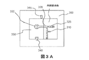
図3Aはアンテナ・アセンブリ10が装着されたPCB300の表面を概略的に例示し、図3BはPCB基板上に装着されたアンテナ・アセンブリ10を概略的に例示する。PCB300は、信号を供給する供給ポート310と伝送部200の信号供給ピン211を受け入れる信号供給コネクタ330に供給ポート310を接続する供給線320とを含む。第1の接地ピン・コネクタ340は接地ストリップ220の接地ピン221に接続するために設けられており、第2の接地ピン・コネクタ345は接地面230の接地ピン231に接続するために設けられている。第1の接地ピン・コネクタ340および第2の接地ピン・コネクタ345はPCB300の接地面に接続されている。インピーダンス整合部品325が供給線320上に設けられている。電子部品を装着するための接続部が設けられていないクリアランス領域350が信号供給コネクタ330の周りに設けられている。接地面230内の開口部236が、信号供給コネクタ330との位置が合うように設けられている。
3A schematically illustrates the surface of the
図4Aおよび図4Bは、図2のPCB基板300の前面側に表示パネル410が装着されたPCB基板300を概略的に例示する。アンテナ・アセンブリ10は、表示パネル410に対して、伝送部200が表示パネル410の後方に配置され、放射部100が表示パネル410の前方に配置されるように、配置されている。伝送部200の信号ストリップ210および接地ストリップ220の長さがもたらす高さでは障害物がないので、アンテナ・アセンブリ10のアンテナ部100は表示パネル410の上方を越えて配置することが可能になり、信号ストリップ110および接地ストリップ120が伝送部200に対して延伸する向きが垂直になっているので、アンテナ・アセンブリ10の放射素子140は表示パネル410の前方に配置することが可能になる。
4A and 4B schematically illustrate the
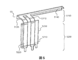
図5は、本発明の第2の実施形態に係るアンテナ・アセンブリ50の概略的な図である。アンテナ・アセンブリ50は、無線周波数信号を放射する放射部5100とアンテナ・アセンブリ50が装着されたプリント回路基板(PCB)の供給線から放射部5100に信号を供給する伝送部5200とを含む。第2の実施形態のアンテナ・アセンブリ50が第1の実施形態のアンテナ・アセンブリ10と異なる点は、伝送部の接地面5230が、信号供給ストリップ5210および接地ストリップ5220に対して、信号供給ストリップ5210に対する放射部5100の放射ストリップ5140と同じ側に位置していることである。
FIG. 5 is a schematic view of an
図6は、本発明の第3の実施形態に係るアンテナ・アセンブリ60の概略的な図である。アンテナ・アセンブリ60は、無線周波数信号を放射する放射部6100とアンテナ・アセンブリ60が装着されたプリント回路基板(PCB)の供給線から放射部6100に信号を供給する伝送部6200とを含む。第3の実施形態のアンテナ・アセンブリ60が第2の実施形態のアンテナ・アセンブリ50と異なる点は、伝送部6200の接地面6230の一部が折り曲げられて、接地面6230の主要部分から、アンテナ・アセンブリ60の放射部6100の信号ストリップ6110および接地ストリップ6120に平行に放射部6100の放射ストリップ6140に向かって延伸していることである。
FIG. 6 is a schematic view of an
図7は、本発明の第4の実施形態に係るアンテナ・アセンブリ70の概略的な図である。アンテナ・アセンブリ70は、無線周波数信号を放射する放射部7100とアンテナ・アセンブリ70が装着されたプリント回路基板(PCB)の供給線から放射部7100に信号を供給する伝送部7200とを含む。第4の実施形態のアンテナ・アセンブリ70が第1の実施形態のアンテナ・アセンブリ10と異なる点は、伝送部7200の接地面7230に2つの接地コネクタ・ピン7231および7232が設けられており、信号ストリップ7210は、より幅広であり、並びに少し曲げられていてもよいことである。これによって、アセンブリがより頑強にすることが可能になる。接地コネクタ・ピン7231と7232は曲げられてもよく、それによって、アンテナ・アセンブリをPCB上に装着する際、並びに、例えば半田付けによってPCBに固定する際に、アンテナ・アセンブリをより確実に保持できる。
FIG. 7 is a schematic view of an
図8Aおよび8Bは、本発明の第5の実施形態に係るアンテナ・アセンブリ80の概略的な図である。本発明のこの実施形態において、アンテナ・アセンブリは、接地導体を有するコプレーナ導波路(CPWG)によって信号が供給される。アンテナ・アセンブリ80は、無線周波数信号を放射する放射部8100と信号ストリップ8210によってCPWGから放射部8100に信号を供給する伝送部8200とを含む。本発明のこの実施形態において、伝送部8200は接地素子および信号ストリップ8210を含む。この接地素子は複数の第1の接地面部分を含み、複数の第1の接地面部分の各々は、信号ストリップ8210の各々の側端から離間され、その側端から離れる方向に延伸して折り返されて第1の接地面部分に平行な第2の接地面8230を形成している。第2の接地面8230は、信号ストリップ8210の主面と第1の接地面部分の主面とに対向しており、この主面から離間されている。接地素子には、PCBの接地部に接続するための4つの接続部812が設けられている。
8A and 8B are schematic views of an
放射部8100は、伝送部の信号ストリップ8210から延伸する信号ストリップ8110と伝送部の接地面8230から延伸する接地ストリップ8120とを含む。信号ストリップ8110および接地ストリップ8120が、伝送部の信号線ストリップ8210および接地面8230に対して約90°の角度で曲げられている。放射ストリップ8140が、信号ストリップ8110の端部および接地ストリップ8120の端部に接続して、IFA型アンテナを形成している。放射ストリップ8140は、その長手方向の軸に沿って約90°の角度で折り曲げられている。
図9は、本発明の実施形態のうちの任意の実施形態に係る3つのアンテナ・アセンブリ910、920および930が装着されたPCB9300を有する電子装置900の俯瞰図である。第1のアンテナ・アセンブリ910は、ディスプレイ940の後方でPCB9300に接続され、アンテナ・アセンブリ910の伝送部がディスプレイ940の後方に配置され、放射素子915がディスプレイ940の上方および前方に配置されるようになっている。第2のアンテナ・アセンブリ920は、複数のLED945のセットの後方でPCB9300に接続され、アンテナ・アセンブリ920の伝送部が複数のLED945のセットの後方に配置され、放射素子925が複数のLED945のセットの上方および前方に配置されるようになっている。第3のアンテナ・アセンブリ930は、複数の複数の押しボタン948のセットの後方でPCB9300に接続され、アンテナ・アセンブリ930の伝送部が複数の押しボタン948のセットの後方に配置され、放射素子935が複数の押しボタン948のセットの上方および前方に配置されるようになっている。
FIG. 9 is an overhead view of an
本発明の実施形態によって、PCB上のグランドクリアランス領域の面積を激減させることが可能になり、他の部品の集積化のためのスペースを広く空けることができる。本発明の実施形態に従うアンテナ・アセンブリを実装することによって、主要基板の前面側に配置された様々な任意の障害物、例えば複数のLEDおよび機械式押しボタンの障害物のようなもの、表示板、または、その他のプラスチック製および金属製のパーツを避けることができ、それによりアンテナの放射性能を改善できる。 According to the embodiment of the present invention, the area of the ground clearance region on the PCB can be drastically reduced, and a space for integrating other components can be widened. By mounting the antenna assembly according to the embodiment of the present invention, various arbitrary obstacles arranged on the front side of the main board, such as obstacles of a plurality of LEDs and mechanical push buttons, a display board Or other plastic and metal parts can be avoided, thereby improving the radiation performance of the antenna.
更に、本発明の実施形態に係るアンテナ・アセンブリは、通常の製造技術を用いて、例えば打抜き加工処理によって、低コストで製造できる。 Furthermore, the antenna assembly according to the embodiment of the present invention can be manufactured at a low cost by using a normal manufacturing technique, for example, by a punching process.
また、本発明の実施形態に係るアンテナ・アセンブリは、PCBの縁端部分だけではなく、PCBの内側部分のRF送信機出力部の近くに配置でき、それによって、単一の金属製パーツとしてアンテナ・アセンブリと一体化される伝送線によって挿入損失を低減できる。この一体化される伝送線はインピーダンス整合線としても機能でき、プリント伝送線や集中定数素子(インダクタ、キャパシタ)を用いて主要基板上にインピーダンス整合をもたらす必要性を回避できる。 In addition, the antenna assembly according to the embodiment of the present invention can be arranged not only at the edge portion of the PCB but also near the RF transmitter output of the inner portion of the PCB, thereby making the antenna as a single metal part. -Insertion loss can be reduced by the transmission line integrated with the assembly. This integrated transmission line can also function as an impedance matching line, avoiding the need to provide impedance matching on the main board using printed transmission lines or lumped elements (inductors, capacitors).
本発明の実施形態に係るアンテナ・アセンブリは、モノポールとしても、ダイポールとしても動作可能である。 The antenna assembly according to the embodiment of the present invention can operate as a monopole or a dipole.
以上、本発明を特定の実施形態について説明したが、本発明は、これらの特定の実施形態には限定されず、本発明の範囲内に在る種々の変更は当業者に明らかであろう。 Although the present invention has been described above with reference to specific embodiments, the present invention is not limited to these specific embodiments, and various modifications within the scope of the present invention will be apparent to those skilled in the art.
例えば、上述の例をセットトップ・ボックスについて説明したが、本発明が、アンテナを用いたその他の任意の無線電子通信装置に適用できることは理解されるであろう。 For example, while the above example has been described for a set-top box, it will be understood that the present invention is applicable to any other wireless electronic communication device using an antenna.
上述の、例としてのみに示された、特許請求の範囲の請求項のみによって特定される本発明の範囲を限定する意図のない実施例を参照すれば、当業者には、多数の更なる変更および変形が自ずと示唆されるであろう。特に、相異なる実施形態から得られる相異なる特徴を、もし適切であれば、交換してもよい。 Many further modifications will occur to those skilled in the art with reference to the above-described examples, which are given by way of example only and are not intended to limit the scope of the invention, which is specified only by the claims. And deformation will naturally be suggested. In particular, different features obtained from different embodiments may be interchanged if appropriate.
開口部236は、接地面230内に信号ストリップ210とPCBとの接続部に面する接地面230の部分に設けられている。これによって接地面230とPCBの供給線との電気的な接触を回避できる。信号ストリップ210には、PCBの供給線の対応する接続部に接続するためのピン211が設けられている。接地ストリップ220には、PCBの接地面上の対応する接続部に接続するためのピン221が設けられており、拡張接地面230には、PCBの接地面上の対応する接続部に接続するためのピン231が設けられている。
The
図4Aおよび図4Bは、図2のPCB基板300の前面側に表示パネル410が装着されたPCB基板300を概略的に例示する。アンテナ・アセンブリ10は、表示パネル410に対して、伝送部200が表示パネル410の後方に配置され、放射部100が表示パネル410の前方に配置されるように、配置されている。伝送部200の信号ストリップ210および接地ストリップ220の長さがもたらす高さでは障害物がないので、アンテナ・アセンブリ10の放射部100は表示パネル410の上方を越えて配置することが可能になり、信号ストリップ110および接地ストリップ120が伝送部200に対して延伸する向きが垂直になっているので、アンテナ・アセンブリ10の放射素子140は表示パネル410の前方に配置することが可能になる。
4A and 4B schematically illustrate the
Claims (17)
放射部と、
該放射部に供給する伝送部であって、該伝送部が前記回路基板に接続可能な信号供給素子と接地素子とを有する、該伝送部と、
を備え、
前記接地素子は、前記信号供給素子と並んで長手方向に延伸する第1の接地部分と該第1の接地部分から横方向に延伸する拡張接地部分とを含み、該拡張接地部分は、折曲され前記信号供給素子および前記第1の接地部分の向こう側に延伸して前記信号供給素子から離間された接地面を形成し、該拡張接地部分が前記回路基板の接地接続部に接続可能である、前記アンテナ・アセンブリ。 An antenna assembly that can be mounted on a circuit board,
A radiation part;
A transmission unit for supplying to the radiating unit, the transmission unit including a signal supply element connectable to the circuit board and a ground element; and
With
The ground element includes a first ground part extending in a longitudinal direction along with the signal supply element, and an extended ground part extending in a lateral direction from the first ground part, and the extended ground part is bent. And extending to the other side of the signal supply element and the first ground portion to form a ground plane spaced from the signal supply element, and the extended ground portion can be connected to a ground connection portion of the circuit board. The antenna assembly.
回路基板と、該回路基板上に装着された請求項1〜12のうちのいずれか一項に記載のアンテナ・アセンブリと、を備え、
前記アンテナ・アセンブリが、前記伝送部の前記信号供給素子と前記接地素子の前記第1の接地部分とが前記回路基板の表面から遠ざかって延伸するように装着される、前記電子通信装置。 An electronic communication device,
A circuit board and the antenna assembly according to any one of claims 1 to 12 mounted on the circuit board,
The electronic communication device, wherein the antenna assembly is mounted such that the signal supply element of the transmission unit and the first grounding portion of the grounding element extend away from the surface of the circuit board.
Applications Claiming Priority (4)
| Application Number | Priority Date | Filing Date | Title |
|---|---|---|---|
| EP14306372.5 | 2014-09-05 | ||
| EP14306372.5A EP2993729A1 (en) | 2014-09-05 | 2014-09-05 | Antenna assembly and electronic device comprising said antenna assembly |
| EP14306755.1A EP3016204A1 (en) | 2014-11-03 | 2014-11-03 | Antenna assembly and electronic device comprising said antenna assembly |
| EP14306755.1 | 2014-11-03 |
Publications (2)
| Publication Number | Publication Date |
|---|---|
| JP2016059043A true JP2016059043A (en) | 2016-04-21 |
| JP2016059043A5 JP2016059043A5 (en) | 2018-10-04 |
Family
ID=53871991
Family Applications (1)
| Application Number | Title | Priority Date | Filing Date |
|---|---|---|---|
| JP2015174318A Withdrawn JP2016059043A (en) | 2014-09-05 | 2015-09-04 | Antenna assembly and electronic device comprising antenna assembly |
Country Status (7)
| Country | Link |
|---|---|
| US (1) | US20160072189A1 (en) |
| EP (1) | EP2993731A1 (en) |
| JP (1) | JP2016059043A (en) |
| KR (1) | KR20160029688A (en) |
| CN (1) | CN105406166A (en) |
| AU (1) | AU2015215891A1 (en) |
| HK (1) | HK1222477A1 (en) |
Families Citing this family (7)
| Publication number | Priority date | Publication date | Assignee | Title |
|---|---|---|---|---|
| EP3240105A1 (en) * | 2016-04-25 | 2017-11-01 | Thomson Licensing | Apparatus including the antenna device |
| EP3264522A1 (en) * | 2016-06-30 | 2018-01-03 | Thomson Licensing | Antenna on smart card and interconnection device |
| EP3264872A1 (en) | 2016-06-30 | 2018-01-03 | Thomson Licensing | Radio frequency interconnection device |
| JP2018074263A (en) * | 2016-10-25 | 2018-05-10 | 旭硝子株式会社 | Vehicle antenna and window pane with antenna |
| EP3336963A1 (en) * | 2016-12-16 | 2018-06-20 | Thomson Licensing | Edge mount low-profile radio frequency antenna |
| CN108448230B (en) * | 2018-01-25 | 2020-12-15 | 瑞声科技(南京)有限公司 | Antenna system and communication terminal |
| CN113241524A (en) * | 2021-04-16 | 2021-08-10 | 深圳市玛雅通讯设备有限公司 | Antenna embedded in screen internal structure, design method and application thereof |
Family Cites Families (11)
| Publication number | Priority date | Publication date | Assignee | Title |
|---|---|---|---|---|
| US5184143A (en) * | 1989-06-01 | 1993-02-02 | Motorola, Inc. | Low profile antenna |
| SE516474C2 (en) * | 1999-11-19 | 2002-01-22 | Allgon Ab | Antenna device and communication device comprising such an antenna device |
| JP2002151928A (en) * | 2000-11-08 | 2002-05-24 | Toshiba Corp | Antenna, and electronic equipment incorporating the antenna |
| WO2004102733A2 (en) * | 2003-05-09 | 2004-11-25 | Etenna Coporation | Multiband antenna with parasitically-coupled resonators |
| US7623079B2 (en) * | 2004-06-30 | 2009-11-24 | Denso Corporation | Vehicle antenna, monitor display device having vehicle antenna, an method of forming vehicle antenna |
| US7450072B2 (en) * | 2006-03-28 | 2008-11-11 | Qualcomm Incorporated | Modified inverted-F antenna for wireless communication |
| CN201156585Y (en) * | 2008-01-24 | 2008-11-26 | 速码波科技股份有限公司 | Short circuit type monopolar antenna |
| TWI390796B (en) * | 2008-09-09 | 2013-03-21 | Arcadyan Technology Corp | Solid dual band antenna device |
| US8144072B2 (en) * | 2009-08-04 | 2012-03-27 | Auden Techno Corp. | Multi-band antenna for notebook computer |
| CN201528044U (en) * | 2009-11-19 | 2010-07-14 | 纬创资通股份有限公司 | Antenna module and circuit board employing same |
| CN102938494B (en) * | 2011-08-15 | 2016-08-10 | 智易科技股份有限公司 | Dual-band antenna |
-
2015
- 2015-08-20 AU AU2015215891A patent/AU2015215891A1/en not_active Abandoned
- 2015-08-24 EP EP15182093.3A patent/EP2993731A1/en not_active Withdrawn
- 2015-08-28 CN CN201510541292.4A patent/CN105406166A/en not_active Withdrawn
- 2015-09-02 KR KR1020150124212A patent/KR20160029688A/en unknown
- 2015-09-04 JP JP2015174318A patent/JP2016059043A/en not_active Withdrawn
- 2015-09-04 US US14/845,630 patent/US20160072189A1/en not_active Abandoned
-
2016
- 2016-09-09 HK HK16110733.3A patent/HK1222477A1/en unknown
Also Published As
| Publication number | Publication date |
|---|---|
| US20160072189A1 (en) | 2016-03-10 |
| CN105406166A (en) | 2016-03-16 |
| EP2993731A1 (en) | 2016-03-09 |
| AU2015215891A1 (en) | 2016-03-24 |
| HK1222477A1 (en) | 2017-06-30 |
| KR20160029688A (en) | 2016-03-15 |
Similar Documents
| Publication | Publication Date | Title |
|---|---|---|
| JP2016059043A (en) | Antenna assembly and electronic device comprising antenna assembly | |
| US10673142B2 (en) | Antenna module | |
| US9252475B2 (en) | Adaptor for connecting a microstrip line to a waveguide using a conductive patch and a stub hole | |
| US9214733B2 (en) | Antenna device | |
| CN106532275B (en) | Antenna device | |
| US9825350B2 (en) | Assembly of circuit boards and electronic device comprising said assembly | |
| US9748660B2 (en) | Antenna with multiple feed points | |
| US20120146876A1 (en) | Surface mount device antenna module | |
| JP2015023394A (en) | Wireless module | |
| US8593368B2 (en) | Multi-band antenna and electronic apparatus having the same | |
| US9231307B2 (en) | Monopole antenna | |
| TWI458176B (en) | Flexographic printing antenna | |
| US20060176218A1 (en) | Gain-adjustable antenna | |
| EP3016204A1 (en) | Antenna assembly and electronic device comprising said antenna assembly | |
| TWI572094B (en) | Antenna structure | |
| EP2993729A1 (en) | Antenna assembly and electronic device comprising said antenna assembly | |
| EP3425728A1 (en) | Connector assembly | |
| TWI770851B (en) | Antenna device | |
| JP7247614B2 (en) | Antenna device and wireless communication device | |
| US20160079673A1 (en) | Chip Antenna Module | |
| TWI626787B (en) | Antenna structure and wireless communication device with same | |
| KR101626940B1 (en) | Antenna structure | |
| JP2011233282A (en) | Connector for wireless antenna | |
| US20170229780A1 (en) | Planar printed antenna and system | |
| BR102015021486A2 (en) | ANTENNA AND ELECTRONIC DEVICE ASSEMBLY UNDERSTANDING THE ANTENNA ASSEMBLY |
Legal Events
| Date | Code | Title | Description |
|---|---|---|---|
| RD03 | Notification of appointment of power of attorney |
Free format text: JAPANESE INTERMEDIATE CODE: A7423 Effective date: 20160603 |
|
| RD04 | Notification of resignation of power of attorney |
Free format text: JAPANESE INTERMEDIATE CODE: A7424 Effective date: 20160610 |
|
| A521 | Request for written amendment filed |
Free format text: JAPANESE INTERMEDIATE CODE: A523 Effective date: 20180820 |
|
| A621 | Written request for application examination |
Free format text: JAPANESE INTERMEDIATE CODE: A621 Effective date: 20180820 |
|
| A761 | Written withdrawal of application |
Free format text: JAPANESE INTERMEDIATE CODE: A761 Effective date: 20190118 |