EP2993731A1 - Antenna assembly and electronic device comprising said antenna assembly - Google Patents
Antenna assembly and electronic device comprising said antenna assembly Download PDFInfo
- Publication number
- EP2993731A1 EP2993731A1 EP15182093.3A EP15182093A EP2993731A1 EP 2993731 A1 EP2993731 A1 EP 2993731A1 EP 15182093 A EP15182093 A EP 15182093A EP 2993731 A1 EP2993731 A1 EP 2993731A1
- Authority
- EP
- European Patent Office
- Prior art keywords
- ground
- antenna assembly
- circuit board
- radiating
- ground portion
- Prior art date
- Legal status (The legal status is an assumption and is not a legal conclusion. Google has not performed a legal analysis and makes no representation as to the accuracy of the status listed.)
- Withdrawn
Links
Images


Classifications
-
- H—ELECTRICITY
- H01—ELECTRIC ELEMENTS
- H01Q—ANTENNAS, i.e. RADIO AERIALS
- H01Q9/00—Electrically-short antennas having dimensions not more than twice the operating wavelength and consisting of conductive active radiating elements
- H01Q9/04—Resonant antennas
- H01Q9/16—Resonant antennas with feed intermediate between the extremities of the antenna, e.g. centre-fed dipole
- H01Q9/20—Two collinear substantially straight active elements; Substantially straight single active elements
-
- H—ELECTRICITY
- H01—ELECTRIC ELEMENTS
- H01Q—ANTENNAS, i.e. RADIO AERIALS
- H01Q1/00—Details of, or arrangements associated with, antennas
- H01Q1/12—Supports; Mounting means
- H01Q1/22—Supports; Mounting means by structural association with other equipment or articles
- H01Q1/24—Supports; Mounting means by structural association with other equipment or articles with receiving set
- H01Q1/241—Supports; Mounting means by structural association with other equipment or articles with receiving set used in mobile communications, e.g. GSM
- H01Q1/242—Supports; Mounting means by structural association with other equipment or articles with receiving set used in mobile communications, e.g. GSM specially adapted for hand-held use
- H01Q1/243—Supports; Mounting means by structural association with other equipment or articles with receiving set used in mobile communications, e.g. GSM specially adapted for hand-held use with built-in antennas
-
- H—ELECTRICITY
- H01—ELECTRIC ELEMENTS
- H01Q—ANTENNAS, i.e. RADIO AERIALS
- H01Q1/00—Details of, or arrangements associated with, antennas
- H01Q1/48—Earthing means; Earth screens; Counterpoises
-
- H—ELECTRICITY
- H01—ELECTRIC ELEMENTS
- H01Q—ANTENNAS, i.e. RADIO AERIALS
- H01Q1/00—Details of, or arrangements associated with, antennas
- H01Q1/52—Means for reducing coupling between antennas; Means for reducing coupling between an antenna and another structure
- H01Q1/526—Electromagnetic shields
-
- H—ELECTRICITY
- H01—ELECTRIC ELEMENTS
- H01Q—ANTENNAS, i.e. RADIO AERIALS
- H01Q9/00—Electrically-short antennas having dimensions not more than twice the operating wavelength and consisting of conductive active radiating elements
- H01Q9/04—Resonant antennas
- H01Q9/30—Resonant antennas with feed to end of elongated active element, e.g. unipole
- H01Q9/42—Resonant antennas with feed to end of elongated active element, e.g. unipole with folded element, the folded parts being spaced apart a small fraction of the operating wavelength
Landscapes
- Engineering & Computer Science (AREA)
- Computer Networks & Wireless Communication (AREA)
- Physics & Mathematics (AREA)
- Electromagnetism (AREA)
- Support Of Aerials (AREA)
- Details Of Aerials (AREA)
- Waveguide Aerials (AREA)
Abstract
Description
- The present invention relates to an antenna assembly and a wireless electronic device comprising said antenna assembly.
- Electronic wireless devices including mobile telephones, tablets set-top boxes and gateway devices contain an increasing number of electronic components in an increasingly reduced space.
-
Figure 10 shows an example of a configuration of electronic components in a set-top box 11. As illustrated, the front side of the circuit board is fully occupied by many electronic components, such as a display device 1, an infra-red sensor 2, a group ofLEDS 3, a group of control push-buttons 4, a SD-card reader 5, andUSB connectors 6. All of these electronic components are aligned along the front edge of the circuit board due to their functionality and usage. - An important functional element of such wireless devices is the antenna for transmission and reception of radio frequency waves. The optimum place for positioning an antenna is at the front of the wireless device. However, the presence of the many other electronic components at the front of a wireless device creates obstacles to the radiation of radio waves and impairs the performance of the antenna. Moreover, in some configurations large areas of ground clearance need to be provided on the circuit board to provide appropriate grounding of the antenna. Because of the presence of the other electronic components it is becoming increasingly difficult to find the required space for ground clearance of antennas at the front side of the circuit board.
- The present invention has been devised with the foregoing in mind.
- A first aspect of the invention provides an antenna assembly mountable on a circuit board, the antenna assembly comprising: a radiating part; a transmission part for feeding the radiating part, the transmission part comprising a signal feed element and a ground element connectable to the circuit board; wherein the ground element comprises a first ground portion extending in a longitudinal direction alongside the signal feed element and an extension ground portion extending laterally from the first ground portion, the extension ground portion being folded to form a ground plane extending over both the signal feed element and the first ground portion and spaced apart from the signal feed element, the extension ground portion being connectable to a ground connection of the circuit board.
- In an embodiment the first ground portion and the extension ground portion are formed as a single grounding unit.
- In an embodiment, the signal feed element and the first ground portion extend parallel to one another.
- In an embodiment, the signal feed element operates in a microstrip mode.
- In an embodiment, the signal feed element is fed by a coplanar waveguide with ground.
- In an embodiment the extension ground element is folded to provide a ground plane on each side of the signal feed element.
- In an embodiment, a transmission line interface is provided for connecting the signal feed element to the circuit board, wherein an aperture is defined in the extension ground portion at the part of the extension ground portion facing towards the transmission line interface.
- In an embodiment, the radiating element comprises an Inverted F Antenna.
- In an embodiment, the radiating part comprises a ground element extending from the first ground portion of the transmission part and a signal element extending from the signal feed element of the transmission part and a radiating element extending perpendicularly to the ground element and the signal element.
- In an embodiment, the radiating element is folded along its longitudinal axis.
- In an embodiment, the radiating element comprises a monopole type antenna
- In an embodiment, the extension ground portion is folded along a further axis such that it extends parallel to the ground element and the signal element of the radiating element.
- In an embodiment, the ground extension portion is located on an opposite side of the signal feed element and the first ground portion of the transmission part, to the radiating element.
- In an embodiment, the ground extension portion is located on the same side of the signal feed element and the first ground portion of the transmission part, as the radiating element.
- In an embodiment the radiating element is a monopole. In another embodiment the radiating element is a dipole.
In an embodiment the transmission part is configured to adapt the impedance of the radiating part. For example, the impedance of the radiating part is adapted to match the input impedance of the transmission part. In one embodiment the height of the transmission part is set to a quarter wavelength. - Another aspect of the invention provides an antenna assembly mountable on a circuit board, the antenna assembly comprising: a radiating part; a transmission part for feeding the radiating part, the transmission part comprising a signal feed element and a ground element connectable to the circuit board; wherein: the ground element comprises a first ground portion extending alongside the signal feed element and a ground plane extending over both the signal feed element and the first ground portion and spaced apart from the signal feed element, the ground plane being connectable to a ground connection of the circuit board.
- The first ground portion and the ground plane may be formed as a single grounding unit.
- A second aspect of the invention provides an electronic communication device comprising a circuit board and an antenna assembly according to any preceding claim mounted on the circuit board, the antenna assembly being mounted such that the a signal feed element and a first ground portion of the transmission part extend away from the surface of the circuit board.
- In an embodiment, the circuit board is provided with at least one electronic component at the front of the circuit board and the radiating part is arranged to extend from the transmission part beyond the electronic component to the front of the electronic component and to face outwards from the electronic communication device, the transmission part being disposed behind the electronic component.
- In an embodiment, the electronic comprises at least one of a display board, an LED, an infra-red sensor, a control unit, and a USB connector.
- In an embodiment, the circuit board comprises a clearance area devoid of electronic components, the clearance area being disposed behind the antenna assembly.
- In an embodiment, the electronic communication device is a gateway device or a set top box.
- A further aspect of the invention provides an antenna assembly mountable on a circuit board, the antenna assembly comprising: a radiating part; a transmission part for feeding the radiating part, the transmission part comprising a signal feed element and a ground element connectable to the circuit board; wherein the ground element comprises an extension ground element, folded away from the ground element such that it extends from the ground element over the signal feed element and the ground element to form a ground plane spaced apart from the signal feed element and connectable to a ground connection of the circuit board.
- Embodiments of the invention will now be described, by way of example only, and with reference to the following drawings in which:
-
FIG. 1 is a schematic diagram of an antenna assembly according to a first embodiment of the invention; -
FIG. 2 is a schematic diagram of the antenna assembly ofFIG. 1 mounted on a PCB; -
FIG. 3A is a planar view of a PCB on which the antenna assembly ofFIG. 1 is mounted; -
FIG. 3B is a perspective view of the antenna assembly ofFIG. 1 mounted on the PCB ofFIG. 3A ; -
FIG. 4A is a perspective view of a PCB, having a display panel, on which the antenna assembly ofFIG. 1 is mounted; -
FIG. 4B is another perspective view of the PCB, having a display panel, on which the antenna assembly ofFIG. 1 is mounted; -
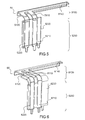
FIG. 5 is a schematic diagram of an antenna assembly according to a second embodiment of the invention; -
FIG. 6 is a schematic diagram of an antenna assembly according to a third embodiment of the invention; -
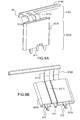
FIG. 7 is a schematic diagram of an antenna assembly according to a fourth embodiment of the invention; -
FIG. 8A and 8B are schematic diagram of an antenna assembly according to a fifth embodiment of the invention; -
FIG. 9 is a perspective view of an electronic device provided with a plurality of antenna assemblies in accordance with embodiments of the invention; and -
FIG. 10 is a perspective view of an example of a wireless electronic device. -
Figure 1 is a schematic diagram of an antenna assembly according to a first embodiment of the invention. Theantenna assembly 10 comprises aradiating part 100 for radiating radio frequency signals and atransmission part 200 for feeding signals from a feed line of a printed circuit board (PCB) on which theantenna assembly 10 is mounted to theradiating part 100. - The
transmission part 200 comprises a signal feed element in the form of asignal strip 210 for feeding signals from the PCB to theradiating part 100 and a ground element comprisingground strip 220 connectable to a ground connection of the PCB. Thesignal strip 210 and theground strip 220 are arranged to extend parallel to one another. Theground strip 220 forms a first ground portion extended by an extension ground portion in the form of extension ground element. The extension ground element extends laterally from one side of theground strip 220 and is curved through an angle of approximately 180° to form aground plane 230 parallel to and spaced apart from the main surfaces of theground strip 220 and thesignal element 210. Theground plane 230 is connectable to a ground connection of the PCB. In this configuration thesignal strip 210 is in a microstrip mode with a finite ground plane provided byground plane 230. - An
aperture 236 is defined in theground plane 230 at the part of theground plane 230 facing the interface between thesignal strip 210 and the PCB. This enables electrical contact between theground plane 230 and the feeding line of the PCB to be avoided. Thesignal strip 210 is provided with apin 211 for connecting to a corresponding connection on the signal feeding line of the PCB. Theground strip 220 is provided with apin 221 for connecting to a corresponding connection on the ground plane of the PCB, and theextension ground plane 230 is provided with apin 231 for connecting to a corresponding connection on the ground plane of the PCB. - The radiating
part 100 comprises asignal strip 110 extending from thesignal strip 210 of the transmitting part, and aground strip 120 extending from theground strip 220 of the transmitting part. Thesignal strip 110 and theground strip 120 are bent at an angle of approximately 90° to thesignal strip 210 and the ground strip of the transmitting part. A radiatingstrip 140 connects the ends of thesignal strip 110 and theground strip 120 to form an IFA type antenna. The radiatingstrip 140 is folded along its longitudinal axis by an angle of approximately 90°. Such a configuration enables the antenna input impedance matching to be optimized. - The
transmission part 200 may also serve as an impedance matching line. Thetransmission part 200 may adapt the impedance of theantenna part 100 to its input impedance. In one particular embodiment the height of the transmission part may correspond to a quarter wavelength. The height of the transmission part is determined by the length of thesignal strip 210 andground strip 220. -
Figure 2 schematically illustrates the antenna assembly ofFigure 1 mounted on aPCB board 300. - The
signal strip 210 and theground strip 220 of thetransmission part 200 of theantenna assembly 10 extend from the surface of thePCB board 300. The radiatingpart 100 of theantenna assembly 200 is thereby raised a height above the surface of thePCB board 300, the height being dependent upon the length of thesignal strip 210 and theground strip 220 of thetransmission part 200. The clearing height enables the radiatingpart 100 to be disposed above an electronic component fitted on thePCB board 300 in front of thetransmission part 200 which would otherwise act as an obstacle to radiation of theradiating strip 140. The extension of thesignal strip 110 and theground strip 120 at a right angle from thesignal strip 210 and theground strip 220 of thetransmission part 200 enables theradiating strip 140 to extend beyond the electronic component thereby providing an obstacle free zone in front of theradiating strip 140. -
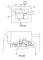
Figure 3A schematically illustrates the surface of thePCB 300 where theantenna assembly 10 is mounted, andFigure 3B schematically illustrates theantenna assembly 10 mounted on the PCB board. ThePCB 300 comprises a feedingport 310 for feeding the signal, afeed line 320 for connecting the feedingport 310 to thesignal feed connector 330 for receiving thesignal feed pin 211 of thetransmission part 200. A firstground pin connector 340 is provided for connecting with theground pin 221 of theground strip 220, and a secondground pin connector 345 is provided for connecting with theground pin 231 of theground plane 230. The firstground pin connector 340 and the secondground pin connector 345 are connected to a ground plane of thePCB 300.Impedance matching components 325 are provided on thefeed line 320. Aclearance area 350 devoid of connections for mounting electronic components is provided around thesignal feed connector 330.Aperture 236 in theground plane 230 is aligned with thesignal feed connector 330. -
Figures 4A and 4B schematically illustrate thePCB board 300 ofFigure 2 fitted with adisplay panel 410 at the front side of thePCB board 300. Theantenna assembly 10 is arranged with respect to thedisplay panel 410 such that thetransmission part 200 is disposed behind thedisplay panel 410 and theantenna part 100 is disposed in front of thedisplay panel 410. The clearance height provided by the length of thesignal feed strip 210 and theground strip 220 of thetransmission part 200 enables theantenna part 100 of theantenna assembly 10 to be disposed over thedisplay panel 410, and the orientation of thesignal strip 110 and theground strip 210 extending perpendicularly to thetransmission part 100 enables the radiatingelement 140 of theantenna part 10 to be disposed in front of thedisplay panel 410. -
Figure 5 is a schematic diagram of anantenna assembly 50 according to a second embodiment of the invention. Theantenna assembly 50 comprises aradiating part 5100 for radiating radio frequency signals and atransmission part 5200 for feeding signals from a feed line of a printed circuit board (PCB) on which theantenna assembly 50 is mounted to theradiating part 5100. Theantenna assembly 50 of the second embodiment differs to theantenna assembly 10 of the first embodiment in that theground plane 5230 of the transmission part is located on the same side of thesignal feed strip 5210 and theground strip 5220 as theradiating element 5140 of theradiating part 5100 relative to thesignal feed strip 5210.. -
Figure 6 is a schematic diagram of anantenna assembly 60 according to a third embodiment of the invention. Theantenna assembly 60 comprises aradiating part 6100 for radiating radio frequency signals and atransmission part 6200 for feeding signals from a feed line of a printed circuit board (PCB) on which theantenna assembly 60 is mounted to theradiating part 6100. Theantenna assembly 60 of the third embodiment differs to theantenna assembly 50 of the second embodiment in that part of theground plane 6230 of thetransmission part 6200 is bent to extend away from the main part of theground plane 6230 parallel to thesignal strip 6110 andground strip 6120 of theradiating part 6100 of theantenna assembly 60 towards the radiatingelement 6140 of theradiating part 6100. -
Figure 7 is a schematic diagram of anantenna assembly 70 according to a fourth embodiment of the invention. Theantenna assembly 70 comprises aradiating part 7100 for radiating radio frequency signals and atransmission part 7200 for feeding signals from a feed line of a printed circuit board (PCB) on which theantenna assembly 70 is mounted to theradiating part 7100. Theantenna assembly 70 of the fourth embodiment differs to theantenna assembly 10 of the first embodiment in that theground plane 7230 of thetransmission part 7200 is provided with two ground connector pins 7231 and 7232, and in that the signal feed strip 7210 is wider, and may be slightly bent. This enables a more rigid assembly to be provided. Ground connector pins 7231 and 7232 may be bent to ensure better hold of the antenna when it is being mounted on the PCB and when it is being fixed to the PCB, for example by soldering. -
Figure 8A and 8B are schematic diagrams of anantenna assembly 80 according to a fifth embodiment of the invention. In this embodiment of the invention the antenna assembly is fed by a coplanar waveguide with ground (CPWG). Theantenna assembly 80 comprises aradiating part 8100 for radiating radio frequency signals and atransmission part 8200 for feeding signals from a CPWG to theradiating part 8100 by afeed line strip 8210. In this embodiment of the invention thetransmission part 8200 comprises a ground element and afeed line strip 8210. The ground element comprises first ground plane portions each extending in a direction away from and spaced apart from respective side edges of thefeed line strip 8210 and folded to form asecond ground plane 8230 parallel to the first ground plane portions. Thesecond ground plane 8230 faces towards and is spaced apart from major surface of thefeed line strip 8210 and the major surfaces of the first ground plane portions. The ground element is provided with fourconnections 812 for connection to a ground of the PCB - The radiating
part 8100 comprises asignal strip 8110 extending from thesignal strip 8210 of the transmitting part, and aground strip 8120 extending from theground plane 8230 of the transmitting part. Thesignal strip 8110 and theground strip 8120 are bent at an angle of approximately 90° to thefeed line strip 8210 and theground plane 8230 of the transmitting part. Aradiating strip 8140 connects the ends of thesignal strip 8110 and theground strip 8120 to form an IFA type antenna. Theradiating strip 8140 is folded along its longitudinal axis by an angle of approximately 90°. -
Figure 9 is a perspective view of anelectronic device 900 having aPCB 9300, on which are mounted threeantenna assemblies first antenna assembly 910 is connected to thePCB 9300 behind adisplay 940 such that the transmission part of theantenna assembly 910 is located behind the display and theradiating element 915 is disposed above and in front of thedisplay 940. Thesecond antenna assembly 920 is connected to thePCB 9300 behind a set of LEDs 945 such that the transmission part of theantenna assembly 920 is located behind the set of LEDs 945 and theradiating element 925 is disposed above and in front of the set of LEDs 945. Thethird antenna assembly 930 is connected to thePCB 9300 behind a set ofpush buttons 948 such that the transmission part of theantenna assembly 930 is located behind the set ofpush buttons 948 and theradiating element 935 is disposed above and in front of the set ofpush buttons 948 . - Embodiments of the invention enable the ground clearance surface area on the PCB to be drastically reduced, freeing more space for the integration of other components. Any obstructions and obstacles placed in the front side of a main board, such as a barrier of LEDS and mechanical push-buttons, a display board or other plastic and metal parts, can be by-passed implementing an antenna assembly according to embodiments of the invention enabling thus an improved radiation performance of the antenna.
- Moreover the antenna assembly according to embodiments of the invention can be manufactured at reduced cost, using common manufacturing technologies, for example by stamping process.
- In addition an antenna assembly according to embodiments of the invention can be placed not only at the edge of a PCB but towards the inner part of the PCB, close to RF transceiver output, thereby reducing insertion losses by virtue of the transmission line being integrated with the antenna assembly in a single metal part. The integrated transmission line may also serve as an impedance matching line, avoiding the need to provide impedance matching on the main board using printed transmission line or lumped components (inductors, capacitors).
- The antenna assembly according to embodiments of the invention may operate as a monopole or a dipole.
- Although the present invention has been described hereinabove with reference to specific embodiments, the present invention is not limited to the specific embodiments, and modifications will be apparent to a skilled person in the art which lie within the scope of the present invention.
- For instance, while the foregoing examples have been described with respect to a set top box it will be appreciated that the invention may be applied to any other wireless electronic communication device employing an antenna.
- Many further modifications and variations will suggest themselves to those versed in the art upon making reference to the foregoing illustrative embodiments, which are given by way of example only and which are not intended to limit the scope of the invention, that being determined solely by the appended claims. In particular the different features from different embodiments may be interchanged, where appropriate.
Claims (17)
- An antenna assembly mountable on a circuit board, the antenna assembly comprising:a radiating part;a transmission part for feeding the radiating part, the transmission part comprising a signal feed element and a ground element connectable to the circuit board; wherein:the ground element comprises a first ground portion extending in a longitudinal direction alongside the signal feed element and an extension ground portion extending laterally from the first ground portion, the extension ground portion being folded to form a ground plane extending over both the signal feed element and the first ground portion and spaced apart from the signal feed element, the extension ground portion being connectable to a ground connection of the circuit board.
- An antenna assembly according to claim 1, wherein the first ground portion and the extension ground portion are formed as a single grounding unit.
- An antenna assembly according to claim 1 or 2, wherein the signal feed element and the first ground portion extend parallel to one another.
- An antenna assembly according to any preceding claim, wherein the signal feed element operates in a microstrip mode.
- An antenna assembly according to any preceding claim, comprising a transmission line interface for connecting the signal feed element to the circuit board, wherein an aperture is defined in the extension ground portion at the part of the extension ground portion facing towards the transmission line interface.
- An antenna assembly according to any preceding claim, wherein the radiating element comprises an Inverted F Antenna.
- An antenna assembly according to claim 6, wherein the radiating part comprises a ground element extending from the first ground portion of the transmission part and a signal element extending from the signal feed element of the transmission part and a radiating element extending perpendicularly to the ground element and the signal element.
- An antenna assembly according to claim 7, wherein the radiating element is folded along its longitudinal axis
- An antenna assembly according to any one of claims 1 to 5, wherein the radiating element comprises a monopole type antenna
- An antenna assembly according to any preceding claim, wherein the extension ground portion is folded along a further axis such that it extends parallel to the ground element and the signal element of the radiating element.
- An antenna assembly according to any preceding claim, wherein the ground extension portion is located on an opposite side of the signal feed element and the first ground portion of the transmission part, to the radiating element.
- An antenna assembly according to any preceding claim, wherein the ground extension portion is located on the same side of the signal feed element and the first ground portion of the transmission part, as the radiating element.
- An electronic communication device comprising:a circuit board and an antenna assembly according to any preceding claim mounted on the circuit board, the antenna assembly being mounted such that the a signal feed element anda first ground portion of a ground element of the transmission part extend away from the surface of the circuit board.
- An electronic communication device according to claim 13 wherein the circuit board is provided with at least one electronic component at the front of the circuit board and the radiating part is arranged to extend from the transmission part beyond the electronic component to the front of the electronic component and to face outwards from the electronic communication device, the transmission part being disposed behind the electronic component.
- An electronic communication device according to claim 14 wherein the at least one electronic component comprises at least one of a display board, an LED, an infra-red sensor, a control unit, and a USB connector.
- An electronic communication device according to any one of claims 13 to 15 wherein the circuit board comprises a clearance area devoid of electronic components, the clearance area being disposed behind the antenna assembly.
- An electronic communication device according to any one of claims 13 to 16 wherein the electronic communication device is a gateway device or a set top box.
Priority Applications (1)
| Application Number | Priority Date | Filing Date | Title |
|---|---|---|---|
| EP15182093.3A EP2993731A1 (en) | 2014-09-05 | 2015-08-24 | Antenna assembly and electronic device comprising said antenna assembly |
Applications Claiming Priority (3)
| Application Number | Priority Date | Filing Date | Title |
|---|---|---|---|
| EP14306372.5A EP2993729A1 (en) | 2014-09-05 | 2014-09-05 | Antenna assembly and electronic device comprising said antenna assembly |
| EP14306755.1A EP3016204A1 (en) | 2014-11-03 | 2014-11-03 | Antenna assembly and electronic device comprising said antenna assembly |
| EP15182093.3A EP2993731A1 (en) | 2014-09-05 | 2015-08-24 | Antenna assembly and electronic device comprising said antenna assembly |
Publications (1)
| Publication Number | Publication Date |
|---|---|
| EP2993731A1 true EP2993731A1 (en) | 2016-03-09 |
Family
ID=53871991
Family Applications (1)
| Application Number | Title | Priority Date | Filing Date |
|---|---|---|---|
| EP15182093.3A Withdrawn EP2993731A1 (en) | 2014-09-05 | 2015-08-24 | Antenna assembly and electronic device comprising said antenna assembly |
Country Status (7)
| Country | Link |
|---|---|
| US (1) | US20160072189A1 (en) |
| EP (1) | EP2993731A1 (en) |
| JP (1) | JP2016059043A (en) |
| KR (1) | KR20160029688A (en) |
| CN (1) | CN105406166A (en) |
| AU (1) | AU2015215891A1 (en) |
| HK (1) | HK1222477A1 (en) |
Cited By (3)
| Publication number | Priority date | Publication date | Assignee | Title |
|---|---|---|---|---|
| EP3264522A1 (en) * | 2016-06-30 | 2018-01-03 | Thomson Licensing | Antenna on smart card and interconnection device |
| EP3316396A1 (en) * | 2016-10-25 | 2018-05-02 | Asahi Glass Company, Limited | Vehicle antenna and window glass |
| EP3336963A1 (en) * | 2016-12-16 | 2018-06-20 | Thomson Licensing | Edge mount low-profile radio frequency antenna |
Families Citing this family (4)
| Publication number | Priority date | Publication date | Assignee | Title |
|---|---|---|---|---|
| EP3240105A1 (en) * | 2016-04-25 | 2017-11-01 | Thomson Licensing | Apparatus including the antenna device |
| EP3264872A1 (en) | 2016-06-30 | 2018-01-03 | Thomson Licensing | Radio frequency interconnection device |
| CN108448230B (en) * | 2018-01-25 | 2020-12-15 | 瑞声科技(南京)有限公司 | Antenna system and communication terminal |
| CN113241524A (en) * | 2021-04-16 | 2021-08-10 | 深圳市玛雅通讯设备有限公司 | Antenna embedded in screen internal structure, design method and application thereof |
Citations (2)
| Publication number | Priority date | Publication date | Assignee | Title |
|---|---|---|---|---|
| US5184143A (en) * | 1989-06-01 | 1993-02-02 | Motorola, Inc. | Low profile antenna |
| US20110032170A1 (en) * | 2009-08-04 | 2011-02-10 | Chi-Ming Chiang | Multi-band antenna for notebook computer |
Family Cites Families (9)
| Publication number | Priority date | Publication date | Assignee | Title |
|---|---|---|---|---|
| SE516474C2 (en) * | 1999-11-19 | 2002-01-22 | Allgon Ab | Antenna device and communication device comprising such an antenna device |
| JP2002151928A (en) * | 2000-11-08 | 2002-05-24 | Toshiba Corp | Antenna, and electronic equipment incorporating the antenna |
| WO2004102733A2 (en) * | 2003-05-09 | 2004-11-25 | Etenna Coporation | Multiband antenna with parasitically-coupled resonators |
| US7623079B2 (en) * | 2004-06-30 | 2009-11-24 | Denso Corporation | Vehicle antenna, monitor display device having vehicle antenna, an method of forming vehicle antenna |
| US7450072B2 (en) * | 2006-03-28 | 2008-11-11 | Qualcomm Incorporated | Modified inverted-F antenna for wireless communication |
| CN201156585Y (en) * | 2008-01-24 | 2008-11-26 | 速码波科技股份有限公司 | Short circuit type monopolar antenna |
| TWI390796B (en) * | 2008-09-09 | 2013-03-21 | Arcadyan Technology Corp | Solid dual band antenna device |
| CN201528044U (en) * | 2009-11-19 | 2010-07-14 | 纬创资通股份有限公司 | Antenna module and circuit board employing same |
| CN102938494B (en) * | 2011-08-15 | 2016-08-10 | 智易科技股份有限公司 | Dual-band antenna |
-
2015
- 2015-08-20 AU AU2015215891A patent/AU2015215891A1/en not_active Abandoned
- 2015-08-24 EP EP15182093.3A patent/EP2993731A1/en not_active Withdrawn
- 2015-08-28 CN CN201510541292.4A patent/CN105406166A/en not_active Withdrawn
- 2015-09-02 KR KR1020150124212A patent/KR20160029688A/en unknown
- 2015-09-04 JP JP2015174318A patent/JP2016059043A/en not_active Withdrawn
- 2015-09-04 US US14/845,630 patent/US20160072189A1/en not_active Abandoned
-
2016
- 2016-09-09 HK HK16110733.3A patent/HK1222477A1/en unknown
Patent Citations (2)
| Publication number | Priority date | Publication date | Assignee | Title |
|---|---|---|---|---|
| US5184143A (en) * | 1989-06-01 | 1993-02-02 | Motorola, Inc. | Low profile antenna |
| US20110032170A1 (en) * | 2009-08-04 | 2011-02-10 | Chi-Ming Chiang | Multi-band antenna for notebook computer |
Cited By (3)
| Publication number | Priority date | Publication date | Assignee | Title |
|---|---|---|---|---|
| EP3264522A1 (en) * | 2016-06-30 | 2018-01-03 | Thomson Licensing | Antenna on smart card and interconnection device |
| EP3316396A1 (en) * | 2016-10-25 | 2018-05-02 | Asahi Glass Company, Limited | Vehicle antenna and window glass |
| EP3336963A1 (en) * | 2016-12-16 | 2018-06-20 | Thomson Licensing | Edge mount low-profile radio frequency antenna |
Also Published As
| Publication number | Publication date |
|---|---|
| US20160072189A1 (en) | 2016-03-10 |
| CN105406166A (en) | 2016-03-16 |
| AU2015215891A1 (en) | 2016-03-24 |
| JP2016059043A (en) | 2016-04-21 |
| HK1222477A1 (en) | 2017-06-30 |
| KR20160029688A (en) | 2016-03-15 |
Similar Documents
| Publication | Publication Date | Title |
|---|---|---|
| EP2993731A1 (en) | Antenna assembly and electronic device comprising said antenna assembly | |
| US9590304B2 (en) | Broadband antenna | |
| US7248224B2 (en) | Antenna device having radiation characteristics suitable for ultrawideband communications | |
| EP3032645B1 (en) | An assembly of circuit boards and electronic device comprising said assembly | |
| EP2565983A2 (en) | Antenna device and electronic apparatus including antenna device | |
| CN109698406A (en) | Multi-antenna module and mobile terminal | |
| US9653794B2 (en) | Broadband antenna and wireless communication device employing same | |
| CN106532275B (en) | Antenna device | |
| US9960479B2 (en) | Antenna device and electronic device | |
| CN108281754A (en) | Multi-antenna device | |
| JP2016105584A (en) | Antenna device, radio communication device and rader device | |
| CN105789820B (en) | Antenna structure and wireless communication device with same | |
| US8593368B2 (en) | Multi-band antenna and electronic apparatus having the same | |
| US9806411B2 (en) | Antenna with high isolation | |
| US9698469B2 (en) | Antenna structure and wireless communication device using the same | |
| US7286086B2 (en) | Gain-adjustable antenna | |
| US10923816B2 (en) | Antenna system of mobile terminal and mobile terminal | |
| US20080094303A1 (en) | Planer inverted-F antenna device | |
| EP3016204A1 (en) | Antenna assembly and electronic device comprising said antenna assembly | |
| KR20070049715A (en) | Small-sized microstrip antenna | |
| EP2037532A1 (en) | Flat dual-band antenna | |
| US20090262027A1 (en) | Dual-Band Antenna | |
| EP2993729A1 (en) | Antenna assembly and electronic device comprising said antenna assembly | |
| US20160079673A1 (en) | Chip Antenna Module | |
| US20150364825A1 (en) | Dual-band three-dimensional antenna |
Legal Events
| Date | Code | Title | Description |
|---|---|---|---|
| PUAI | Public reference made under article 153(3) epc to a published international application that has entered the european phase |
Free format text: ORIGINAL CODE: 0009012 |
|
| AK | Designated contracting states |
Kind code of ref document: A1 Designated state(s): AL AT BE BG CH CY CZ DE DK EE ES FI FR GB GR HR HU IE IS IT LI LT LU LV MC MK MT NL NO PL PT RO RS SE SI SK SM TR |
|
| AX | Request for extension of the european patent |
Extension state: BA ME |
|
| 17P | Request for examination filed |
Effective date: 20160907 |
|
| RBV | Designated contracting states (corrected) |
Designated state(s): AL AT BE BG CH CY CZ DE DK EE ES FI FR GB GR HR HU IE IS IT LI LT LU LV MC MK MT NL NO PL PT RO RS SE SI SK SM TR |
|
| REG | Reference to a national code |
Ref country code: HK Ref legal event code: DE Ref document number: 1222477 Country of ref document: HK |
|
| 17Q | First examination report despatched |
Effective date: 20190617 |
|
| STAA | Information on the status of an ep patent application or granted ep patent |
Free format text: STATUS: THE APPLICATION HAS BEEN WITHDRAWN |
|
| 18W | Application withdrawn |
Effective date: 20190717 |
|
| REG | Reference to a national code |
Ref country code: HK Ref legal event code: WD Ref document number: 1222477 Country of ref document: HK |