JP2015536624A - Dielectric waveguide filter with direct coupling and alternative cross coupling - Google Patents
Dielectric waveguide filter with direct coupling and alternative cross coupling Download PDFInfo
- Publication number
- JP2015536624A JP2015536624A JP2015545172A JP2015545172A JP2015536624A JP 2015536624 A JP2015536624 A JP 2015536624A JP 2015545172 A JP2015545172 A JP 2015545172A JP 2015545172 A JP2015545172 A JP 2015545172A JP 2015536624 A JP2015536624 A JP 2015536624A
- Authority
- JP
- Japan
- Prior art keywords
- block
- dielectric material
- dielectric
- waveguide filter
- resonators
- Prior art date
- Legal status (The legal status is an assumption and is not a legal conclusion. Google has not performed a legal analysis and makes no representation as to the accuracy of the status listed.)
- Pending
Links
Images


Classifications
-
- H—ELECTRICITY
- H01—ELECTRIC ELEMENTS
- H01P—WAVEGUIDES; RESONATORS, LINES, OR OTHER DEVICES OF THE WAVEGUIDE TYPE
- H01P1/00—Auxiliary devices
- H01P1/20—Frequency-selective devices, e.g. filters
- H01P1/207—Hollow waveguide filters
- H01P1/208—Cascaded cavities; Cascaded resonators inside a hollow waveguide structure
- H01P1/2088—Integrated in a substrate
-
- H—ELECTRICITY
- H01—ELECTRIC ELEMENTS
- H01P—WAVEGUIDES; RESONATORS, LINES, OR OTHER DEVICES OF THE WAVEGUIDE TYPE
- H01P1/00—Auxiliary devices
- H01P1/20—Frequency-selective devices, e.g. filters
- H01P1/2002—Dielectric waveguide filters
-
- H—ELECTRICITY
- H01—ELECTRIC ELEMENTS
- H01P—WAVEGUIDES; RESONATORS, LINES, OR OTHER DEVICES OF THE WAVEGUIDE TYPE
- H01P1/00—Auxiliary devices
- H01P1/20—Frequency-selective devices, e.g. filters
- H01P1/207—Hollow waveguide filters
- H01P1/209—Hollow waveguide filters comprising one or more branching arms or cavities wholly outside the main waveguide
-
- H—ELECTRICITY
- H01—ELECTRIC ELEMENTS
- H01P—WAVEGUIDES; RESONATORS, LINES, OR OTHER DEVICES OF THE WAVEGUIDE TYPE
- H01P7/00—Resonators of the waveguide type
- H01P7/10—Dielectric resonators
Landscapes
- Control Of Motors That Do Not Use Commutators (AREA)
Abstract
導電性材料の外層で覆われた誘電材料のブロックを備える誘電体導波管フィルタを提供する。複数の積層共振器は、誘電材料のブロック内の1つまたは複数のスロット、および積層共振器を分離する導電性材料の内層により、誘電材料のブロック内に画定される。導電性材料の内層内の第1および第2のRF信号伝送ウィンドウは、積層共振器の間に直接結合および交差結合のRF信号伝送の両方を提供する。一実施形態では、導波管フィルタは、それぞれが導電性材料の外層で覆われた誘電材料の分離したブロックからなり、それぞれは、複数の共振器を画定し、積層された関係で一緒に結合された、1つまたは複数のスロットを含む。【選択図】図1A dielectric waveguide filter comprising a block of dielectric material covered with an outer layer of conductive material is provided. The plurality of stacked resonators are defined within the block of dielectric material by one or more slots in the block of dielectric material and an inner layer of conductive material separating the stacked resonators. First and second RF signal transmission windows in the inner layer of conductive material provide both direct and cross-coupled RF signal transmission between the stacked resonators. In one embodiment, the waveguide filter consists of separate blocks of dielectric material each covered with an outer layer of conductive material, each defining a plurality of resonators coupled together in a stacked relationship One or more slots. [Selection] Figure 1
Description
関連出願および同時係属出願の相互参照
本出願は、2012年11月28日に出願された米国特許仮出願第61/730,615号の出願日および開示の利益を主張し、それらの内容全体が、本明細書に引用された参考文献のすべてを参照により本明細書に組み込まれる。
This application claims the filing date and benefit of US Provisional Application No. 61 / 730,615 filed Nov. 28, 2012, the entire contents of which are incorporated herein by reference. All of the references cited herein are hereby incorporated by reference.
また本出願は、2011年5月9日に「帯域幅を調整するための構造および方法を有する誘電体導波管フィルタ」という名称で出願された米国特許出願第13/103,712号、2011年12月3日に「直接結合および代替交差結合を有する誘電体導波管フィルタ」と言う名称で出願された米国特許出願第13/373,862号、ならびに2012年8月2日に「調整された誘電体導波管フィルタおよび調整方法」という名称で出願された米国特許出願第13/564,822号の出願日および開示の利益を主張し、本出願はそれらの一部継続出願であり、それらの内容全体が、本明細書に引用された参考文献のすべてを参照により本明細書に組み込まれる。 This application is also filed on May 9, 2011, under US patent application Ser. No. 13 / 103,712, 2011, filed under the title “Dielectric Waveguide Filter with Structure and Method for Tuning Bandwidth”. US patent application Ser. No. 13 / 373,862 filed on Dec. 3, 2012 under the name “Dielectric Waveguide Filter with Direct Coupling and Alternative Cross Coupling”, and “Regulation” on Aug. 2, 2012. Claims the benefit of the filing date and disclosure of US patent application Ser. No. 13 / 564,822 filed under the title of “Dielectric Waveguide Filters and Tuning Methods”, which is a continuation-in-part of those applications. The entire contents of which are hereby incorporated by reference in their entirety.
本発明は、一般に誘電体導波管フィルタに関し、より詳細には、直接結合および代替交差結合を有する誘電体導波管フィルタに関する。 The present invention relates generally to dielectric waveguide filters, and more particularly to dielectric waveguide filters having direct coupling and alternative cross coupling.
本発明は、Heineらによる米国特許第5,926,079号に開示されたタイプの誘電体導波管フィルタに関し、複数の共振器はモノブロックの長さに沿って長手方向に離間され、また複数のスロット/ノッチは、モノブロックの長さに沿って長手方向に離間され、複数の共振器間に複数の橋を画定し、これは複数の共振器間に直接誘導/容量結合を提供する。 The present invention relates to a dielectric waveguide filter of the type disclosed in US Pat. No. 5,926,079 by Heine et al., Wherein a plurality of resonators are spaced longitudinally along the length of the monoblock, and The plurality of slots / notches are spaced longitudinally along the length of the monoblock and define a plurality of bridges between the plurality of resonators, which provide direct inductive / capacitive coupling between the plurality of resonators. .
Heineらによる米国特許第5,926,079号に開示されたタイプの導波管フィルタの減衰特性は、導波管フィルタの一端または両端に配置された追加の共振器の形でゼロの組込みを通して増加されることが可能である。しかし追加の共振器の組込みに関連した不利益は、追加の共振器の組込みによりフィルタの長さも増加し、これは一部の適用では、例えば顧客のマザーボード上の空間制限に起因して望ましくないまたは可能でないことがあるということである。 The attenuation characteristics of a waveguide filter of the type disclosed in US Pat. No. 5,926,079 by Heine et al. Is achieved through the incorporation of zero in the form of an additional resonator located at one or both ends of the waveguide filter. It can be increased. However, the disadvantages associated with incorporating additional resonators also increase the length of the filter with the incorporation of additional resonators, which is undesirable in some applications due to space limitations on the customer's motherboard, for example. Or it may not be possible.
またフィルタの減衰特性も、例えばVangalaらによる米国特許第7,714,680号に開示されたような共振器を直接結合および交差結合の両方によって増加されることが可能である。米国特許第7,714,680号は、各金属化パターンにより一部が生成された共振器の誘導直接結合および四交差結合の両方を伴うモノブロックフィルタを開示し、各金属化パターンは、フィルタの頂面上に画定され、共振器の貫通孔の選択された貫通孔の間に延在して共振器の開示された直接結合および交差結合を提供する。 The attenuation characteristics of the filter can also be increased by both direct and cross coupling resonators such as disclosed in US Pat. No. 7,714,680 by Vangala et al. U.S. Pat. No. 7,714,680 discloses a monoblock filter with both inductive direct coupling and four-cross coupling of resonators partially created by each metallization pattern, each metallization pattern being a filter Defined between the top surfaces of the resonators and extending between selected through holes of the resonator through holes to provide the disclosed direct and cross coupling of the resonators.
Vangalaらによる米国特許第7,714,680号に開示され、金属化パターンの頂面からなるタイプの直接結合および交差結合は、スロットのみを含み頂面の金属化パターンがない、Heineらによる米国特許第5,926,079号に開示されたタイプの導波管フィルタには適用できない。 US Pat. No. 7,714,680 to Vangala et al., The type of direct and cross-bonding consisting of the top surface of the metallization pattern is the United States by Heine et al., Which contains only slots and no metallization pattern on the top surface. It cannot be applied to a waveguide filter of the type disclosed in Japanese Patent No. 5,926,079.
したがって本発明は、導波管フィルタの長さが増加することなく、またはフィルタの頂面上に金属化パターンを使用することなく、導波管フィルタの減衰特性の増加が可能な、直接結合および恣意的に交差結合した共振器を備える誘電体導波管フィルタに関する。 Therefore, the present invention provides a direct coupling and increase in the attenuation characteristics of the waveguide filter without increasing the length of the waveguide filter or without using a metallization pattern on the top surface of the filter. The present invention relates to a dielectric waveguide filter comprising an arbitrarily cross-coupled resonator.
本発明は、導電性材料の外層で覆われた複数の外面を含む誘電材料のブロックと、誘電材料のブロックの中に延在する1つまたは複数のスロットおよび複数の積層共振器を分離する導電性材料の内層により、誘電材料のブロック内に画定された複数の積層共振器と、誘電材料のブロック上に画定された少なくとも第1のRF信号入力/出力電極と、導電性材料の内層内に画定され、複数の積層共振器間にRF信号を伝送するための直通経路を画定する、第1のRF信号伝送ウィンドウとを備える、誘電体導波管フィルタに関する。 The present invention provides a block of dielectric material that includes a plurality of outer surfaces covered with an outer layer of conductive material and one or more slots that extend into the block of dielectric material and a plurality of stacked resonators. An inner layer of conductive material includes a plurality of stacked resonators defined in the block of dielectric material, at least a first RF signal input / output electrode defined on the block of dielectric material, and an inner layer of conductive material. A dielectric waveguide filter comprising: a first RF signal transmission window defined and defining a direct path for transmitting an RF signal between a plurality of stacked resonators.
一実施形態では、第1および第2のスロットは、誘電材料のブロックの1つまたは複数の外面の中に延在し、誘電材料のブロックを少なくとも第1および第2の積層共振器ならびに第3および第4の積層共振器に分離し、第1のRF信号伝送ウィンドウは、第1の積層共振器と第2の積層共振器との間の導電性材料の前記内層内に画定され、第2のRF信号伝送ウィンドウは、導電性材料の内層内に画定され、第3の積層共振器と第4の積層共振器との間にRF信号を前記伝送するための間接経路を画定する。 In one embodiment, the first and second slots extend into one or more outer surfaces of the block of dielectric material and pass the block of dielectric material to at least the first and second stacked resonators and the third. And a first RF signal transmission window is defined in the inner layer of conductive material between the first and second stacked resonators, and The RF signal transmission window is defined in the inner layer of conductive material and defines an indirect path for transmitting the RF signal between the third and fourth stacked resonators.
一実施形態では、第2のRF信号入力/出力電極は、第1のRF信号入力/出力電極が誘電体導波管フィルタを通るRF信号を伝送するための概ね長円形状の直接経路を画定する関係に対して、誘電材料のブロック内に画定される。 In one embodiment, the second RF signal input / output electrode defines a generally oval direct path for the first RF signal input / output electrode to transmit the RF signal through the dielectric waveguide filter. Are defined within a block of dielectric material.
一実施形態では、誘電材料のブロックは長手軸を画定し、第1および第2のRF信号入力/出力電極は、誘電材料のブロックを通って延在するそれぞれの第1および第2の貫通孔によって画定され、第1および第2のスロットならびに第1および第2の貫通孔は、長手軸の方向に対して横方向に延在し、第1および第2の貫通孔は、導電性材料の内層の対向する側面上に正反対の方向に同一線上の関係で配置される。 In one embodiment, the block of dielectric material defines a longitudinal axis, and the first and second RF signal input / output electrodes are each first and second through-holes extending through the block of dielectric material. The first and second slots and the first and second through holes extend transversely to the direction of the longitudinal axis, and the first and second through holes are formed of the conductive material. Arranged on opposite side surfaces of the inner layer in the same direction in the opposite direction.
一実施形態では、誘電材料のブロックは、誘電材料の第1および第2の分離したブロックからなり、それぞれは、導電性材料の外層で覆われた複数の外面を含み、誘電材料の第1および第2の分離したブロックが互いに積層される際に導電性材料の内層を画定し、第1のスロットは、誘電材料の第1のブロック内に画定され、誘電材料の第1のブロックを第1および第3の共振器に分離し、第2のスロットは、誘電材料の第2のブロック内に画定され、誘電材料の第2のブロックを第2および第4の共振器に分離し、それぞれの第1および第2のRF信号伝送ウィンドウは、誘電材料のそれぞれの第1および第2のブロックの外面を覆う、導電性材料の層内のそれぞれのウィンドウによって画定される。 In one embodiment, the block of dielectric material comprises first and second separate blocks of dielectric material, each including a plurality of outer surfaces covered with an outer layer of conductive material, wherein the first and second layers of dielectric material An inner layer of conductive material is defined when the second separate blocks are stacked together, a first slot is defined in the first block of dielectric material, and the first block of dielectric material is first in the first block. And a second resonator, wherein a second slot is defined in the second block of dielectric material, and separates the second block of dielectric material into second and fourth resonators, respectively. The first and second RF signal transmission windows are defined by respective windows in the layer of conductive material covering the outer surface of the respective first and second blocks of dielectric material.
また本発明は、導電性材料の層で覆われた複数の外面、ならびに1つまたは複数の外面の中に延在し、誘電材料の第1のブロックを少なくとも第1および第2の共振器に分離する少なくとも第1のスロットを含む、誘電材料の第1のブロックと、誘電材料の第1のブロックの一端に画定された第1のRF信号入力/出力電極と、導電性材料の層で覆われた複数の外面、ならびに1つまたは複数の外面の中に延在し、誘電材料の第2のブロックを少なくとも第3および第4の共振器に分離する、少なくとも第2のスロットを含む、誘電材料の第2のブロックであって、誘電材料の第2のブロックは、誘電材料の第1のブロック上に積層される関係であり、第1および第4の共振器は互いに積層され、第2および第3の共振器は互いに積層され、第1の直接の概ね長円形状のRF信号伝送経路は、導波管フィルタを通って画定される、誘電材料の第2のブロックとを備える、誘電体導波管フィルタに関する。 The invention also includes a plurality of outer surfaces covered with a layer of conductive material, and extending into the one or more outer surfaces, wherein the first block of dielectric material is at least the first and second resonators. A first block of dielectric material including at least a first slot to separate, a first RF signal input / output electrode defined at one end of the first block of dielectric material, and a layer of conductive material. A plurality of external surfaces, and at least a second slot extending into the one or more external surfaces and separating the second block of dielectric material into at least third and fourth resonators. A second block of material, wherein the second block of dielectric material is stacked on the first block of dielectric material, the first and fourth resonators are stacked on each other, and the second block And the third resonator are stacked on each other, RF signal transmission path 1 direct substantially oval shape is defined through the waveguide filter, and a second block of dielectric material, relates to a dielectric waveguide filter.
一実施形態では、第1の直接RF信号伝送経路は、第2の積層共振器と第3の積層共振器との間に配置された第1のRF信号伝送ウィンドウにより部分的に画定される。 In one embodiment, the first direct RF signal transmission path is defined in part by a first RF signal transmission window disposed between the second and third stacked resonators.
一実施形態では、第1の直接RF信号伝送ウィンドウは、誘電材料のそれぞれの第1および第2のブロックの外面を覆う、導電性材料の層内のそれぞれの第1および第2のウィンドウによって画定される。 In one embodiment, the first direct RF signal transmission window is defined by respective first and second windows in the layer of conductive material covering the outer surface of the respective first and second blocks of dielectric material. Is done.
一実施形態では、第2のRF信号伝送ウィンドウは、第1の共振器と第4の共振器との間にRF信号を伝送するための間接経路を提供するために、第1の積層共振器と第4の積層共振器との間に配置される。 In one embodiment, the second RF signal transmission window includes a first stacked resonator to provide an indirect path for transmitting an RF signal between the first resonator and the fourth resonator. And the fourth laminated resonator.
一実施形態では、第2のRF信号伝送ウィンドウは、誘電材料のそれぞれの第1および第2のブロックの外面を覆う、導電性材料の層内のそれぞれの第3および第4のウィンドウによって画定される。 In one embodiment, the second RF signal transmission window is defined by respective third and fourth windows in the layer of conductive material covering the outer surface of the respective first and second blocks of dielectric material. The
一実施形態では、第2のRF信号入力/出力電極は、誘電材料の第2のブロックの一端に画定され、誘電材料の第1のブロックの一端に画定された第1のRF信号入力/出力電極に正反対の方向の関係で位置付けられ、第1および第2のRF信号入力/出力電極は、誘電材料のそれぞれの第1および第2のブロックを通って延在するそれぞれの第1および第2の貫通孔によって画定される。 In one embodiment, the second RF signal input / output electrode is defined at one end of the second block of dielectric material and the first RF signal input / output defined at one end of the first block of dielectric material. Positioned diametrically opposite the electrodes, the first and second RF signal input / output electrodes are respectively first and second extending through respective first and second blocks of dielectric material. Defined by the through hole.
一実施形態では、それぞれの第1および第2の段部は、誘電材料の第1および第2のブロックのそれぞれの一端に画定され、それぞれの第1および第2の貫通孔は、それぞれの第1および第2の段部を通って延在する。 In one embodiment, each first and second step is defined at one end of each of the first and second blocks of dielectric material, and each first and second through-hole is a respective first. Extending through the first and second steps.
本発明は、さらに第1の長手軸を画定し、導電性材料の層で覆われた複数の外面、誘電材料の第1のブロック内に画定され、第1の長手軸の方向と反対の方向に延在し、誘電材料の第1のブロックを第1の長手軸に沿って延在する第1の複数の共振器に分離する第1の複数のスロット、ならびに誘電材料の第1のブロックの一端に画定された第1の段部を含む、誘電材料の第1のブロックと、誘電材料の第1のブロックの段部内に画定された第1のRF信号入力/出力貫通孔と、導電性材料の第1のブロックに対して着座された誘電材料の第2のブロックであって、誘電材料の第2のブロックは、第2の長手軸を画定し、導電性材料の層で覆われた複数の外面、誘電材料の第2のブロック内に画定され、第2の長手軸の方向と反対の方向に延在し、誘電材料の第2のブロックを第2の長手軸に沿って延在する第2の複数の共振器に分離する、第2の複数のスロット、ならびに誘電材料の第2のブロックの一端に画定された第2の段部を含む、誘電材料の第2のブロックと、誘電材料の第2のブロックの段部内に画定された第2のRF信号入力/出力貫通孔と、第1および第2のRF信号入力/出力貫通孔と誘電材料の第1および第2のブロック内の複数の共振器の組合せによって画定された、第1の直接RF信号伝送経路とを備える、誘電体導波管フィルタに関する。 The present invention further defines a first longitudinal axis, a plurality of outer surfaces covered with a layer of conductive material, defined in a first block of dielectric material, and in a direction opposite to the direction of the first longitudinal axis A first plurality of slots extending to and separating a first block of dielectric material into a first plurality of resonators extending along a first longitudinal axis; and a first block of dielectric material A first block of dielectric material including a first step defined at one end; a first RF signal input / output through hole defined in the step of the first block of dielectric material; A second block of dielectric material seated against the first block of material, wherein the second block of dielectric material defines a second longitudinal axis and is covered with a layer of conductive material A plurality of outer surfaces, defined in a second block of dielectric material, extending in a direction opposite to the direction of the second longitudinal axis. A second plurality of slots separating the second block of dielectric material into a second plurality of resonators extending along a second longitudinal axis, and at one end of the second block of dielectric material A second block of dielectric material including a defined second step; a second RF signal input / output through hole defined in the step of the second block of dielectric material; A dielectric waveguide comprising two RF signal input / output through holes and a first direct RF signal transmission path defined by a combination of a plurality of resonators in the first and second blocks of dielectric material Regarding filters.
一実施形態では、第1の直接RF信号伝送経路は、誘電材料の第1のブロック内の第1の複数の共振器の第1の共振器と誘電材料の第2のブロック内の第2の複数の共振器の第1の共振器との間に配置された、第1の直接RF信号伝送手段により部分的に画定される。 In one embodiment, the first direct RF signal transmission path includes a first resonator in the first plurality of resonators in the first block of dielectric material and a second in the second block of dielectric material. Defined in part by a first direct RF signal transmission means disposed between the first resonator of the plurality of resonators.
一実施形態では、第1の直接RF信号伝送手段は、誘電材料のそれぞれの第1および第2のブロックの外面を覆う導電性材料の層内に画定された、それぞれの第1および第2のウィンドウによって画定される。 In one embodiment, the first direct RF signal transmission means is each first and second defined in a layer of conductive material overlying the outer surface of each first and second block of dielectric material. Defined by the window.
一実施形態では、第1の直接RF信号伝送手段は、誘電材料の第1のブロック内の第1の複数の共振器の第2の共振器から、誘電材料の第2のブロック内の第2の複数の共振器の第2の共振器に、RF信号を伝送するための第1の間接結合経路を画定する。 In one embodiment, the first direct RF signal transmission means includes a second resonator in the second block of dielectric material from a second resonator of the first plurality of resonators in the first block of dielectric material. A first indirect coupling path for transmitting an RF signal is defined in the second resonator of the plurality of resonators.
一実施形態では、第1の間接RF信号伝送線手段は、誘電材料のそれぞれの第1および第2のブロックの複数の外面を覆う、導電性材料の層内に画定されたそれぞれの第3および第4のウィンドウによって画定される。 In one embodiment, the first indirect RF signal transmission line means has a respective third and defined in a layer of conductive material covering a plurality of outer surfaces of the respective first and second blocks of dielectric material. Defined by a fourth window.
一実施形態では、第1の直接RF信号伝送経路は、概ね長円形状である。 In one embodiment, the first direct RF signal transmission path is generally oval shaped.
本発明の他の利点および特徴は、本発明の好ましい実施形態の以下の詳述、添付図面、および添付の特許請求の範囲からより容易に明らかになろう。 Other advantages and features of the present invention will become more readily apparent from the following detailed description of the preferred embodiments of the invention, the accompanying drawings, and the appended claims.
本発明のこれらの特徴および他の特徴は、以下の添付図面の以下の説明によって最も良く理解されることが可能である。 These and other features of the present invention can be best understood by the following description of the accompanying drawings.
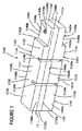
図1、2、および3は、本発明による直接結合および代替交差結合/間接結合の特徴ならびに特性の両方を組み込む、導波管フィルタ1100を示す。
1, 2, and 3 illustrate a
示された実施形態では、導波管フィルタ1100は、導波管フィルタ1100を形成するように積層された関係で一緒に結合された、誘電材料1101および1103の1対の分離した概ね平行六面体形状のモノブロックから作成される。
In the illustrated embodiment, the
底部モノブロック1101は、例えばセラミックなどの誘電材料の適切な中実ブロックまたはコアからなり、対向する長手方向の水平外面1102aおよび1104a、水平外面1102aおよび1104aに垂直な関係で配置され、水平外面1102aと1104aとの間に延在する、対向する長手方向側面の垂直外面1106aおよび1108a、ならびに長手方向の水平外面1102aおよび1104aならびに長手方向の垂直外面1102aおよび1102bに概ね垂直な関係で配置され、長手方向の水平外面1102aと1104aおよび長手方向の垂直外面1102aと1102bとの間に延在する、対向する横方向端側面の垂直外端面1110aおよび1112aを含む。
The
したがって示された実施形態では、それぞれの面1102a、1104a、1106a、および1108aは、モノブロック1101の長手軸L1(図3)と同じ方向に延在し、それぞれの端面1110aおよび1112aは、モノブロック1101の長手軸L1の方向に横または垂直方向に延在する。
Thus, in the illustrated embodiment, each
また頂部モノブロック1103も、例えばセラミックなどの誘電材料の適切な中実ブロックまたはコアからなり、対向する長手方向の水平外面1102bおよび1104b、水平外面1102bおよび1104bに垂直な関係で配置され、水平外面1102bと1104bとの間に延在する、対向する長手方向側面の垂直外面1106bおよび1108b、ならびに水平外面1102bおよび1104bならびに長手方向側面の垂直外面1106bおよび1108bに垂直な関係で配置され、水平外面1102bと1104bおよび長手方向側面の垂直外面1106bと1108bとの間に延在する、対向する横方向端側面の垂直外面1110bおよび1112bを含む。
The
したがって示された実施形態では、それぞれの面1102b、1104b、1106b、および1108bは、モノブロック1103の長手軸L2(図3)と同じ方向に延在し、それぞれの面1110bおよび1112bは、モノブロック1103の長手軸L2の方向に横または垂直方向に延在する。
Thus, in the illustrated embodiment, each
モノブロック1101および1103は、それぞれの第1および第2の複数の共振部(空洞またはセルまたは共振器とも呼ばれる)1114、1116、および1118、ならびに1120、1121、および1122を含み、これらはそれぞれのモノブロック1101および1103の長手軸L1およびL2の長さに沿って長手方向に離間され、それぞれのモノブロック1101および1103の長手軸L1およびL2と同一線上にかつ同じ方向に延在し、垂直外面1106aの中に切り込まれた、またより具体的にはモノブロック1101の面1102a、1104a、および1106aの中に切り込まれた、モノブロック1101内の複数の(またより具体的には図1、2、および3の実施形態では1対の)離間された概して平行な垂直切込みまたはスロット1124a、ならびに垂直外面1106bの中に切り込まれた、またより具体的にはモノブロック1103の面1102b、1104b、および1106bの中に切り込まれた、モノブロック1103内の1対の離間された概して平行な垂直切込みまたはスロット1124bによって互いに離間される。
したがって示された実施形態では、それぞれの垂直切込みまたはスロット1124aおよび1124bは、それぞれのモノブロック1101およびb1103の長手軸L1およびL2の方向に概して横または垂直方向に延在する。
Thus, in the illustrated embodiment, each vertical cut or
図3に示されたように、底部モノブロック1101内の一方の切込み1124aは、共振器1114と共振器1116との間にRF信号を通過および伝送するために、モノブロック1101上に第1の橋またはスルーウェイまたは通路1128を画定する一方で、モノブロック1101内の他方の切込み1124aは、共振器1116と共振器1118との間にRF信号を通過および伝送するために、モノブロック1101上に第2の橋またはスルーウェイまたは通路1130を画定する。
As shown in FIG. 3, one
同様に、また図3にも示されたように、モノブロック1103内の一方の切込み1124bは、共振器1122と共振器1121との間にRF信号を通過および伝送するために、モノブロック1103上に第1の橋またはスルーウェイまたは通路1134を画定する一方で、モノブロック1103内の他方の切込み1124bは、共振器1121と共振器1120との間にRF信号を通過および伝送するために、モノブロック1103上に第2の橋またはスルーウェイまたは通路を画定する。
Similarly, as also shown in FIG. 3, one
モノブロック1101、またより具体的にはモノブロック1101の端部共振器1114は、示された実施形態では、長手面1102aの概ねL字形状の窪んだ、もしくは溝の付いた、もしくは肩が付いた、もしくは刻み目のある領域または部分、対向する側面1106aおよび1108a、ならびにそこから誘電セラミック材料が取り除かれたまたは誘電セラミック材料がないモノブロック1101の側端面1112aを備える、端段部1136aをさらに備え画定する。
The
同様にモノブロック1103、またより具体的にはモノブロック1103の端部共振器1122は、示された実施形態では、長手面1104bの概ねL字形状の窪んだ、もしくは溝の付いた、もしくは肩が付いた、もしくは刻み目のある領域または部分、対向する側面1106bおよび1108b、ならびにそこから誘電材料が取り除かれたまたは誘電材料がないモノブロック1103の側端面1112bを備える、端段部1136bをさらに備え画定する。
Similarly, the
言い換えれば、示された実施形態では、それぞれの段部1136aおよび1136bは、それぞれのモノブロック1101および1103の残余部の高さまたは厚さより小さい高さまたは厚さを有する、それぞれのモノブロック1101および1103の端部または領域内に、それぞれのモノブロック1101および1103の端部または領域によって画定される。
In other words, in the illustrated embodiment, each
さらに示された実施形態では、それぞれの端段部1136aおよび1136bは、それぞれのモノブロック1101および1103の上に画定されたそれぞれの端部共振器1114および1122の概ねL字形状の窪んだ、もしくは刻み目のある部分を備え、これは、それぞれのモノブロック1101および1103の面1102aおよび1104bに配置された、またはそれぞれのモノブロック1101および1103の面1102aおよび1104bの内方に方向付けられ、それぞれのモノブロック1101および1103の面1102aおよび1104bから離間され、それぞれのモノブロック1101および1103の面1102aおよび1104bに平行な、それぞれの第1の概ね水平な面1140aおよび1140b、ならびにそれぞれのモノブロック1101および1103のそれぞれの側端面1110aおよび1112aならびに1110bおよび1112bに配置された、またはそれぞれのモノブロック1101および1103のそれぞれの側端面1110aおよび1112aならびに1110bおよび1112bの内方に方向付けられ、それぞれのモノブロック1101および1103のそれぞれの側端面1110aおよび1112aならびに1110bおよび1112bから離間され、それぞれのモノブロック1101および1103のそれぞれの側端面1110aおよび1112aならびに1110bおよび1112bに平行な、それぞれの第2の概ね垂直な面または壁1142aおよび1142bを含む。
In a further illustrated embodiment, each
さらに、また本明細書に示されていない、または詳細に説明されていないが、端段部1136aおよび1136bも、それぞれのモノブロック1101および1103の残余部の高さまたは厚さより大きい高さまたは厚さを有する、それぞれのモノブロック1101および1103の外方に延在する端部または領域によって画定されることが可能であることが理解される。
Further, although not shown or described in detail herein,
加えてモノブロック1101および1103は、それぞれが電気RF信号入力/出力電極を備え、これらは示された実施形態では、それぞれの円筒形状の貫通孔1146aおよび1146b(図2および3)の形であり、これらはそれぞれのモノブロック1101および1103の本体を通って延在し、またより具体的には、そのそれぞれの段部1136aおよび1136bを通って、さらにより具体的には、それぞれの段部1136aおよび1136bの面1140aと1140bとの間、ならびにそれぞれのモノブロック1101および1103の面1104aと1102bとの間にあり、かつそれぞれの段部1136aおよび1136bのそれぞれの面1140aおよび1140b、ならびにそれぞれのモノブロック1101および1103のそれぞれの面1104aおよび1102bに概ね垂直な関係で、それぞれのモノブロック1101および1103の中に画定されたそれぞれの端部共振器1114および1122の本体を通って延在する。
In addition, the
さらにより具体的には、それぞれの入力/出力貫通孔1146aおよび1146bは、それぞれのモノブロック1101および1103のそれぞれの横側端面1112aおよび1112bから離間され、それぞれのモノブロック1101および1103のそれぞれの横側端面1112aおよび1112bに概ね平行であり、それぞれの段面1140aおよび1140b内に配置され、それぞれの段面1140aおよび1140bで終了するそれぞれの概ね円形の開口1147aおよび1147b、ならびにそれぞれのブロック面1104aおよび1102b(図3)で終了するそれぞれの対向する開口1148aおよび1148bを画定する。
Even more specifically, the respective input / output through
またそれぞれのRF信号入力/出力貫通孔1146aおよび1146bも、それぞれの段壁または面1142aおよび1142bから概ね離間され、それぞれの段壁または面1142aおよび1142bに平行な関係で、またそれぞれのモノブロック1101および1103の長手軸に概ね垂直または横方向である関係で、それぞれのモノブロック1101および1103の内側に配置され、それぞれのモノブロック1101および1103の内側に位置付けられ、それぞれのモノブロック1101および1103の内側を通って延在する。
Also, the respective RF signal input / output through
モノブロック1101の外面1102a、1104a、1106a、1108a、1110a、および1112aのすべて、切込み1124aを画定するモノブロック1101の外面、ならびにRF信号入力/出力貫通孔1146aを画定するモノブロック1101の内側円筒面は、例えば銀などの適切な導電性材料で覆われる。但し、面1140a上にあり、貫通孔1146aにより面1140a内に画定された開口1147aを包囲するリング形状領域1170a(図2および3)を含む、以下により詳細に説明される領域を除く。
All of the
同様に、モノブロック1103の外面1102b、1104b、1106b、1110b、および1112bのすべて、切込み1124bを画定するモノブロック1103の外面、ならびにRF信号入力/出力貫通孔1146bを画定するモノブロック1103の内側円筒面も、例えば銀などの適切な導電性材料で覆われる。但し、面1140b上にあり、貫通孔1146bにより面1140b内に画定された開口1147bを包囲するリング形状領域1170b(図1、2および3)を含む、以下により詳細に説明される領域を除く。
Similarly, all of the
一層さらにモノブロック1101および1103は、それぞれの貫通孔1146aおよび1146bによりそれぞれの面1140aおよび1140b内に画定された、それぞれの開口1147aおよび1147bから外方に突出するそれぞれのRF信号入力/出力コネクタ1400を備える。
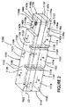
図1および2に示されたように、分離したモノブロック1101および1103は、上に置き当接し積層された関係で互いに結合され積層されて、分離したモノブロック1101および1103が、より具体的には、それらの各共振器が、以下により詳細に説明されるように互いに対して上に置き当接し積層された関係で配置される手法で、導波管フィルタ1100を画定し形成する。
As shown in FIGS. 1 and 2, the separated
具体的には、モノブロック1101および1103は互いに対して結合された関係であり、図1、2、および3に示されたように、頂部モノブロック1103の長手方向の水平外面1102bは、底部モノブロック1101の長手方向の水平外面1104a上に着座され当接される。
Specifically,
さらにより具体的には、モノブロック1101および1103は互いに対して積層された関係であり、モノブロック1101の水平面1104aは、モノブロック1103の水平面1102bに当接され、導波管フィルタ1100の内側の長さおよび幅に延在する導電性材料の中心内層1150(図1および2)は、モノブロック1101の面1104aとモノブロック1103の面1102bに挟まれ、それぞれのモノブロック1101および1103の外面1104aおよび1102bの長さおよび幅を覆う導電性材料の層によって画定され、モノブロック1101の長手方向側面の垂直外面1106aは、モノブロック1103の長手方向側面の垂直外面1106bと同一線上に位置合わせされ、モノブロック1101のスロット1124aは、モノブロック1103上のスロット1124bと同一線上に位置合わせされ、モノブロック1101の対向する長手方向側面の垂直外面1108aは、モノブロック1103の長手方向側面の垂直外面1108bと同一平面に位置合わせされ、モノブロック1101の横方向側面の垂直外面1110aは、モノブロック1103の横方向端側面の垂直外面1110bと同一平面に位置合わせされ、モノブロック1101の対向する横方向端側面の垂直外面1112aは、モノブロック1103の対向する横方向端側面の垂直外面1112bと同一平面に位置合わせされる。
Even more specifically, the
したがって図1および2に示されたような関係では、それぞれのモノブロック1101および1103上のそれぞれの端段部1136aおよび1136bは、対向し当接し積層された関係で配置され、それぞれのモノブロック1101および1103上のそれぞれの共振器1114および1122は、対向し当接し積層された関係で配置され、それぞれのモノブロック1101および1103上のそれぞれの共振器1116および1121は、対向し当接し積層された関係で配置され、それぞれのモノブロック1101および1103上のそれぞれの共振器1118および1120は、対向し当接し積層された関係で配置される。
Therefore, in the relationship as shown in FIGS. 1 and 2, the respective
したがって、また図2に示されたように、導波管フィルタ1100は、長手軸L3を画定する誘電材料の概ね平行六面体形状のブロックであり、それぞれのモノブロック1101および1103のそれぞれの外面1102aおよび1102bに対応し、長手軸L3と同じ方向に、長手軸L3の上下に、また長手軸L3に概ね平行に延在する、対向し離間された平行な底部および頂部の長手方向の水平外面1102および1104と、それぞれのモノブロック1101および1103のそれぞれの面1104aおよび1102b上の導電性材料の層に対応し、長手軸L3と概ね水平な同一平面の関係で、さらに底部および頂部の長手方向の水平外面1102および1104から離間され、底部および頂部の長手方向の水平外面1102および1104に概ね平行である関係で、導波管フィルタ1100の内側の全長および幅を通って延在する、導電性材料の中心内層1150と、それぞれのモノブロック1101および1103のそれぞれが垂直な同一平面に位置合わせされた面1106aおよび1106bならびに1108aおよび1108bに対応し、長手軸L3と同じ方向に、長手軸L3と反対側に、また長手軸L3に概ね平行に延在する、対向し離間された平行な側面の垂直外面1106および1108と、それぞれのモノブロック1101および1103の垂直に同一平面に位置合わせされた面1110aおよび1110bならびに1112aおよび1112bに対応し、長手軸L3に横または垂直な方向に延在し、長手軸L3と交差する、対向し離間された平行な端側垂直外面1110および1112と、それぞれのモノブロック1101および1103内の垂直な同一線上に位置合わせされた切込みまたはスロット1124aおよび1124bに対応し、長手方向の垂直外面1106から導波管フィルタ1100の中に、また導波管フィルタ1100の本体の中に入る関係で、長手軸L3に横または垂直な方向に延在し、底部および頂部の長手方向の水平面1102および1104内のそれぞれの孔または切取り部内で終了する、導波管フィルタ1100内の1対の離間された平行な切込みまたはスロット1124と、共振器1114および1122と一体化され、示された実施形態では、導波管フィルタ1100の残余部の厚さまたは高さより小さい厚さまたは高さを有する、端部または領域1136とを含む。
Thus, and also as shown in FIG. 2, the
示された実施形態では、端部または領域1136は、長手軸L3の下に配置され、長手軸L3から離間され、導波管フィルタ1100の底部外面1102の内方に延在し、導波管フィルタ1100の底部外面1102から離間され、導波管フィルタ1100の底部外面1102に平行な外面1140aを含む、モノブロック1101内に画定された段部1136aに対応する第1の概ねL字形状の段部または肩部1136aと、長手軸L3の上に配置され、長手軸L3から離間され、導波管フィルタ1100の頂部外面1104の内方に延在し、導波管フィルタ1100の底部外面1104から離間され、導波管フィルタ1100の底部外面1104に平行な外面1140bを含む、モノブロック1103内の段部1136bに対応する、正反対の方向の第2の概ねL字形状の段部または肩部1136bとを画定する。
In the illustrated embodiment, the end or
モノブロック1101内に画定された貫通孔1146aに対応する概ね円筒形状の貫通孔1146aは、長手軸L3に横に垂直な方向に長手軸L3の下にある関係で、段面1140a内に画定された概ね円筒形状の開口1147aと導電性材料の中心層1150との間を、端部1136を通って延在する。
A generally cylindrical through
モノブロック1103内の貫通孔1146bに対応する概ね円筒形状の貫通孔1146bは、貫通孔1146bと同一線にあり貫通孔1146bと正反対の方向の関係で、長手軸L3に横に垂直な方向に長手軸L3の上にある関係で、段面1140b内に画定された概ね円筒形状の開口1147bと導電性材料の中心層1150との間を、端部1136を通って延在する。
A substantially cylindrical through
したがって示された実施形態では、貫通孔1146aおよび1146bは、導電性材料の中心層1150および導波管フィルタ1100の長手軸L3の対向する側面上に正反対の方向に同一線上の関係で、導電性材料の中心層1150および導波管フィルタ1100の長手軸L3に概ね垂直な関係で配置される。
Thus, in the illustrated embodiment, the through-
したがって図2の実施形態では、導波管フィルタ1100のそれぞれの外面1102、1104、1106、1108、1110、1112、それぞれの切込み/スロット1124を画定する導波管フィルタ1100の内面、ならびにそれぞれの貫通孔1146aおよび1146bを画定する導波管フィルタ1100の内面は、導電性材料の層で覆われるまたは被覆される。但し、端部1136のそれぞれの段面1140aおよび1140b内のそれぞれの貫通孔1146aおよび1146bによって画定された、それぞれの開口1147aおよび1147bを包囲する、それぞれの円形またはリング形状の領域1170aおよび1170b1151を除く。
Thus, in the embodiment of FIG. 2, each
導波管フィルタ1100は、第1の内側または内部RF信号伝送ウィンドウまたは手段または結合部1622(図2および3)をさらに備え、これは示された実施形態では、長手軸L3に横方向に延在し、長手軸L3と交差する長方形の形状であり、これは導波管フィルタ1100のそれぞれの共振器1118と1120との間、より具体的には、導波管フィルタ1100を画定するために一緒に結合された、それぞれのモノブロック1101および1103のそれぞれの共振器1118と1120との間に、RF信号を伝送するための直接誘導経路またはウィンドウまたは結合部を提供する。
The
示された実施形態では、ウィンドウ1622は、導電性材料の中心層1150内に画定され、共振器1118と1120との間に配置された中心層1150の領域内に形成された、概ね長方形形状の孔または隙間または開口またはウィンドウを備える。より具体的には、ウィンドウ1622は、それぞれのモノブロック1101および1103のそれぞれの外面1104aおよび1102bを覆い、それぞれの共振器1118および1120の領域においてその上に配置された、導電性材料の層内に形成された、それぞれの概ね長方形形状の孔または隙間または開口またはウィンドウ1622aおよび1622bによって画定される。ウィンドウ1622aおよび1622bは、モノブロック1101および1103が一緒に結合されて導電性材料の中心層1150およびその中にウィンドウ1622を画定する際に、互いに位置合わせされる。
In the illustrated embodiment, the
言い換えると、ウィンドウ1622は、モノブロック1101および1103が一緒に結合される際に互いに位置合わせされると、内側RF信号伝送ウィンドウ1622を画定する、それぞれのモノブロック1101および1103のそれぞれの外面1104aおよび1102b上の誘電材料のそれぞれの概ね長方形形状の領域1622aおよび1622bによって画定される。
In other words, the
この実施形態によれば、共振器1118と1120との間の導波管フィルタ1100の内側に配置されたウィンドウ1622により、導波管フィルタ1100の共振器1118から共振器1120の中にRF信号の内部または内側直接誘導通過または伝送が可能になる。
According to this embodiment, a
加えて導波管フィルタ1100は、共振器1116と1121との間の導波管フィルタ1100の内側に配置された、第1の間接または交差結合内側または内部容量性RF信号伝送ウィンドウまたは手段または結合部1722を備え、これは示された実施形態では、長手軸L3およびウィンドウ1622と同じ方向に、長手軸L3およびウィンドウ1622と同一線上に延在する長方形の形状であり、導波管フィルタ1100のそれぞれの共振器1116と1121との間に、またより具体的には、一緒に結合されたそれぞれのモノブロック1101および1103の共振器1116と1121との間にRF伝送信号を伝送して導波管フィルタ1100を画定する。
In addition, the
示された実施形態では、ウィンドウ1722は、導電性材料の中心層1150内に画定され、共振器1116と1121との間に配置された中心層1150の領域内に形成された、概ね長方形形状の孔または隙間または開口またはウィンドウを備える。したがって、ウィンドウ1722は、それぞれのモノブロック1101および1103のそれぞれの外面1104aおよび1102bを覆い、それぞれの共振器1116および1121の領域内に配置された、導電性材料の層内に形成された、それぞれの概ね長方形形状の孔または隙間または開口またはウィンドウ1722aおよび1722bによって画定される。ウィンドウ1722aおよび1722bは、導電性材料の中心層1150およびその中のウィンドウ1722を画定するために、モノブロック1101および1103が一緒に結合される際に、互いに位置合わせされる。
In the illustrated embodiment, the
言い換えると、ウィンドウ1722は、モノブロック1101および1103が一緒に結合される際に互いに位置合わせされると、内側RF信号伝送ウィンドウ1722を画定する、それぞれのモノブロック1101および1103のそれぞれの外面1104aおよび1102b上に導電性材料のそれぞれの概ね長方形形状の領域1722aおよび1722bによって画定される。
In other words, the
本発明によれば、導波管フィルタ1100は、以下に説明されるように、図2に矢印dで概ね示された、RF信号のための第1の磁気または誘導の概ね長円形状の直接結合RF信号伝送経路を画定する。
In accordance with the present invention, the
まずRF信号は、モノブロック1101内の貫通孔1146aがRF信号入力貫通孔を画定する実施形態では、コネクタ1400および貫通孔1146aの中に伝送される。その後RF信号は、端部1136、より具体的には、モノブロック1101上の端段部1136aの中に、次いでモノブロック1101内の共振器1114の中に、次いでRF信号伝送橋または経路1128を介してモノブロック1101内の共振器1116の中に、次いでRF信号伝送橋または経路1130を介してモノブロック1101内の共振器1118の中に伝送される。
First, the RF signal is transmitted into the
その後、RF信号は、モノブロック1101からモノブロック1103の中に、またより具体的には、モノブロック1101内の共振器1118から共振器1118と1120との間の導波管フィルタ1100の内側に配置された内側容量性RF信号伝送ウィンドウ1622を介して、モノブロック1103内の共振器1120の中に伝送される。
The RF signal is then passed from
その後、RF信号は、RF信号伝送橋または経路1132を介してモノブロック1103内の共振器1121の中に、次いでRF信号伝送橋または経路1134を介してモノブロック1103内の共振器1122の中に、次いでモノブロック1103内の端部1136の中に、またより具体的にはモノブロック1103の段部1136bの中に伝送され、次いでモノブロック1103内の貫通孔1146bがRF信号出力貫通孔を画定する実施形態では、貫通孔1146b、およびモノブロック1103の端部1136内のコネクタ1400を通って出る。
The RF signal is then routed into the
本発明のこの実施形態によれば、導波管フィルタ1100も、図2に矢印cで概ね示されたRF信号のための代替または間接または交差結合RF信号伝送経路を画定し提供する。
In accordance with this embodiment of the invention,
具体的には、交差結合または間接容量性RF信号伝送経路cは、共振器1116と1121との間に配置された内側RF信号伝送手段またはウィンドウ1722によって画定され生成され、これにより直接RF信号のわずかな部分の伝送を、モノブロック1101の共振器1116を通ってモノブロック1103の共振器1121の中に直接伝送できる。
Specifically, a cross-coupled or indirect capacitive RF signal transmission path c is defined and generated by an inner RF signal transmission means or
本発明によれば、またRF信号伝送ウィンドウ1622の領域または大きさが、RF信号伝送ウィンドウ1722の領域または大きさより大きい図3に示されたように、それぞれのモノブロック1101および1103のそれぞれの共振器1118と1120との間にあり、それぞれのモノブロック1101および1103のそれぞれの共振器1118および1120を相互連結させる内部RF信号伝送ウィンドウ1622は、導波管フィルタ1100のそれぞれのモノブロック1101および1103のそれぞれの共振器1116と1121との間にあり、それぞれのモノブロック1101および1103のそれぞれの共振器1116および1121を相互連結させる内部RF信号伝送ウィンドウ1722によって生成され画定された間接容量性交差結合より強い誘導直接RF信号結合を生成するように設計され/大きさにされる。
In accordance with the present invention, and as shown in FIG. 3, the region or size of the RF
図4は、高性能誘電体導波管フィルタ1100の計算された周波数応答を示すグラフであり、これは示された実施形態では、以下の性能特性からなり、以下の性能特性を含む。すなわち、モノブロック1103および1103は、それぞれ誘電率が約37以上の高品質のC14セラミック材料からなり、モノブロック1101および1103は、それぞれおよそ長さ2インチ、幅0.5インチ、高さ1.1インチであり、帯域幅は中心周波数の5パーセント(%)以下であり、許容入力は200ワット(W)以下であり、共振器は約1000〜2000の範囲のQを有し、挿入損失は約マイナス2dB(−2dB)であり、阻止帯域減衰量は約マイナス70dB(−70dB)であり、帯域幅は約40〜100メガヘルツ(MHz)の範囲であり、中心周波数は約2ギガヘルツ(GHz)である。
FIG. 4 is a graph illustrating the calculated frequency response of the high performance
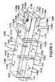
図5は、本発明による誘電体導波管フィルタ2100の別の実施形態であり、これは以下に論じられる1点以外はすべて誘電体導波管フィルタ1100の構造、要素、および機能と同一であり、したがって図1〜3において導波管フィルタ1100の様々な要素を示すために使用された番号は、図5に示された導波管フィルタ2100における同じ要素を同定し示すために使用されており、したがって導波管フィルタ1100の各要素の構造および機能の前の説明は、参照により本明細書に組み込まれ、このような説明が本明細書で完全に説明されたかのように、導波管フィルタ2100に関して図5に同定された各要素に関して本明細書に適用し繰り返される。
FIG. 5 is another embodiment of a
共振器1116と1121との間の導波管フィルタ1100の内側に配置された長方形形状の間接または交差結合の内側または内部容量性RF信号伝送ウィンドウまたは手段または結合部1722が、共振器1116と1121との間の導波管フィルタ2100の内側に配置された、丸みを帯びたまたは円形形状の間接または交差結合の内側または内部容量性RF信号伝送ウィンドウまたは手段または結合部2722を備える、図5に示された導波管フィルタ2100に置換されたという点において、図5に示された導波管フィルタ2100は図1〜3に示された導波管フィルタ1100と異なる。
A rectangular indirect or cross-coupled inner or internal capacitive RF signal transmission window or means or
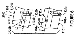
示された実施形態では、ウィンドウ2722は、導電性材料の中心内層1150を画定する導電性材料または金属材料の概ね丸みを帯びたまたは円形形状の領域または部分またはパッチまたはパッドを備え、これは概ねリング形状の領域2723によって囲まれ、概ねリング形状の領域2723は、導電性材料の中心内層1150の導電性材料の残余部から導電性材料2722のウィンドウまたはパッチを隔離し、共振器1116と1121との間に配置された中心層1150の領域内に形成された導電性材料(すなわち誘電材料の領域)を欠く。
In the illustrated embodiment, the window 2722 comprises a generally rounded or circular shaped region or portion or patch or pad of conductive or metallic material that defines a central
したがって、また図6に示されたように、ウィンドウ2722は、それぞれのモノブロック1101および1103のそれぞれの外面1104aおよび1102b上の導電性材料のそれぞれの概ね円形形状の領域または部分またはパッチまたはパッド2722aおよび2722bによって画定され、これはそれぞれの外面1104aおよび1102bのそれぞれのリング形状の領域2723aおよび2723bによって囲まれ、それぞれのリング形状の領域2723aおよび2723bは、それぞれの外面1104aおよび1102bを覆う導電性材料の層の残余部から導電性材料2722aおよび2722bのそれぞれのウィンドウまたはパッチを隔離する、導電性材料(すなわち誘電材料の各領域)を欠く。それぞれのウィンドウ2722aおよび2722bは、それぞれの共振器1116および1121の領域内のそれぞれのモノブロック1101および1103のそれぞれの外面1104aおよび1102b上に配置される。
Thus, and also as shown in FIG. 6, the window 2722 has a respective generally circular shaped region or portion or patch or
ウィンドウ2722aおよび2722bは、モノブロック1101および1103が一緒に結合されて導電性材料の中心層1150およびその中のウィンドウ2722を画定する際に、互いに位置合わせされ連結される。
この実施形態では、交差結合または間接容量性RF信号伝送経路cは、共振器1116と1121との間に配置された、内側RF信号伝送手段またはウィンドウ2722によって画定され生成され、これにより直接RF信号のわずかな部分の伝送を、モノブロック1101の共振器1116を通ってモノブロック1103の共振器1121の中に直接伝送できる。
In this embodiment, the cross-coupled or indirect capacitive RF signal transmission path c is defined and generated by an inner RF signal transmission means or window 2722 disposed between the
本発明は示された実施形態を具体的に参照して教示されたが、本発明の精神および範囲から逸脱することなく形および詳細に変更を行うことができることが、当業者には認識されることが理解される。説明された実施形態は、あらゆる点で例示に過ぎず、限定するとみなされるべきではない。 While the invention has been taught with specific reference to the illustrated embodiments, those skilled in the art will recognize that changes can be made in form and detail without departing from the spirit and scope of the invention. It is understood. The described embodiments are merely exemplary in all respects and should not be construed as limiting.
例えば、これに限定されないが、導波管フィルタのウィンドウ、段部、貫通孔、および切込み/スロットを含む、導波管フィルタのいくつかの要素の構成、大きさ、形状、および場所は、導波管フィルタの特定の適用または所望の性能特性に依存して調節されてもよいことが理解される。 For example, but not limited to, the configuration, size, shape, and location of several elements of a waveguide filter, including, but not limited to, waveguide filter windows, steps, through-holes, and notches / slots, It is understood that the wave tube filter may be adjusted depending on the particular application or desired performance characteristics.
Claims (18)
導電性材料の外層で覆われた複数の外面を含む誘電材料のブロックと、
複数の積層共振器であって、前記誘電材料のブロックの中に延在する1つまたは複数のスロットおよび前記複数の積層共振器を分離する導電性材料の内層により、前記誘電材料のブロック内に画定された、複数の積層共振器と、
前記誘電材料のブロック上に画定された少なくとも第1のRF信号入力/出力電極と、
前記導電性材料の内層内に画定され、前記複数の積層共振器間にRF信号を伝送するための直通経路を画定する、第1のRF信号伝送ウィンドウと
を備える、誘電体導波管フィルタ。 A dielectric waveguide filter comprising:
A block of dielectric material comprising a plurality of outer surfaces covered with an outer layer of conductive material;
A plurality of stacked resonators, wherein one or more slots extending into the dielectric material block and an inner layer of conductive material separating the plurality of stacked resonators are within the block of dielectric material. A plurality of stacked resonators defined;
At least a first RF signal input / output electrode defined on the block of dielectric material;
A dielectric waveguide filter comprising: a first RF signal transmission window defined in an inner layer of the conductive material and defining a direct path for transmitting an RF signal between the plurality of stacked resonators.
誘電材料の第1のブロックであって、導電性材料の層で覆われた複数の外面、ならびに1つまたは複数の前記外面の中に延在し、前記誘電材料の第1のブロックを少なくとも第1および第2の共振器に分離する、少なくとも第1のスロットを含む、誘電材料の第1のブロックと、
前記誘電材料の第1のブロックの一端に画定された第1のRF信号入力/出力電極と、
誘電材料の第2のブロックであって、導電性材料の層で覆われた複数の外面、ならびに1つまたは複数の前記外面の中に延在し、前記誘電材料の第2のブロックを少なくとも第3および第4の共振器に分離する、少なくとも第2のスロットを含み、前記誘電材料の第2のブロックが、前記第1および第4の共振器が互いに積層され、前記第2および第3の共振器が互いに積層され、第1の概ね長円形状のRF信号の直接の伝送経路が、前記導波管フィルタを介して画定される関係で、前記誘電材料の第1のブロックに積層される、誘電材料の第2のブロックと
を備える、誘電体導波管フィルタ。 A dielectric waveguide filter comprising:
A first block of dielectric material extending into the plurality of outer surfaces covered with a layer of conductive material and one or more of the outer surfaces, wherein the first block of dielectric material is at least first A first block of dielectric material comprising at least a first slot that separates into a first and a second resonator;
A first RF signal input / output electrode defined at one end of the first block of dielectric material;
A second block of dielectric material extending into the plurality of outer surfaces covered with a layer of conductive material and one or more of the outer surfaces, wherein the second block of dielectric material is at least first At least a second slot separating the third and fourth resonators, wherein the second block of dielectric material is laminated to the first and fourth resonators, and the second and third resonators Resonators are stacked on top of each other and a first generally oval RF signal direct transmission path is stacked on the first block of dielectric material in a relationship defined through the waveguide filter. A dielectric waveguide filter comprising: a second block of dielectric material.
誘電材料の第1のブロックであって、第1の長手軸を画定し、導電性材料の層で覆われた複数の外面、前記誘電材料の第1のブロック内に画定され、前記第1の長手軸の方向と反対の方向に延在し、前記誘電材料の第1のブロックを前記第1の長手軸に沿って延在する第1の複数の共振器に分離する、第1の複数のスロット、ならびに前記誘電材料の第1のブロックの一端に画定された第1の段部を含む、誘電材料の第1のブロックと、
前記誘電材料の第1のブロックの前記段部内に画定された第1のRF信号入力/出力貫通孔と、
前記誘電性材料の第1のブロックに対して着座された誘電材料の第2のブロックであって、前記誘電材料の第2のブロックが、第2の長手軸を画定し、導電性材料の層で覆われた複数の外面、前記誘電材料の第2のブロック内に画定され、前記第2の長手軸の方向と反対の方向に延在し、前記誘電材料の第2のブロックを前記第2の長手軸に沿って延在する第2の複数の共振器に分離する、第2の複数のスロット、ならびに前記誘電材料の第2のブロックの一端に画定された第2の段部を含む、誘電材料の第2のブロックと、
前記誘電材料の第2のブロックの前記段部内に画定された第2のRF信号入力/出力貫通孔と、
前記第1および第2のRF信号入力/出力貫通孔と前記誘電材料の第1および第2のブロック内の前記複数の共振器の組合せによって画定された、第1の直接RF信号伝送経路と
を備える、誘電体導波管フィルタ。 A dielectric waveguide filter comprising:
A first block of dielectric material, defining a first longitudinal axis, a plurality of outer surfaces covered with a layer of conductive material, defined within the first block of dielectric material, A first plurality of resonators extending in a direction opposite to the direction of the longitudinal axis and separating the first block of dielectric material into a first plurality of resonators extending along the first longitudinal axis; A first block of dielectric material comprising a slot and a first step defined at one end of the first block of dielectric material;
A first RF signal input / output through hole defined in the step of the first block of dielectric material;
A second block of dielectric material seated against the first block of dielectric material, the second block of dielectric material defining a second longitudinal axis and a layer of conductive material A plurality of outer surfaces covered with a second block of dielectric material defined in the second block of dielectric material and extending in a direction opposite to the direction of the second longitudinal axis, wherein the second block of dielectric material is A second plurality of slots that separate into a second plurality of resonators extending along a longitudinal axis of the second material, and a second step defined at one end of the second block of dielectric material, A second block of dielectric material;
A second RF signal input / output through hole defined in the step of the second block of dielectric material;
A first direct RF signal transmission path defined by a combination of the first and second RF signal input / output through holes and the plurality of resonators in the first and second blocks of dielectric material; A dielectric waveguide filter comprising:
Applications Claiming Priority (5)
| Application Number | Priority Date | Filing Date | Title |
|---|---|---|---|
| US201261730615P | 2012-11-28 | 2012-11-28 | |
| US61/730,615 | 2012-11-28 | ||
| US14/088,471 | 2013-11-25 | ||
| US14/088,471 US9130255B2 (en) | 2011-05-09 | 2013-11-25 | Dielectric waveguide filter with direct coupling and alternative cross-coupling |
| PCT/US2013/071859 WO2014085383A1 (en) | 2012-11-28 | 2013-11-26 | Dielectric waveguide filter with direct coupling and alternative cross-coupling |
Related Child Applications (1)
| Application Number | Title | Priority Date | Filing Date |
|---|---|---|---|
| JP2018167603A Division JP6782745B2 (en) | 2012-11-28 | 2018-09-07 | Dielectric waveguide filter with direct coupling and alternative cross coupling |
Publications (2)
| Publication Number | Publication Date |
|---|---|
| JP2015536624A true JP2015536624A (en) | 2015-12-21 |
| JP2015536624A5 JP2015536624A5 (en) | 2017-01-05 |
Family
ID=49724701
Family Applications (2)
| Application Number | Title | Priority Date | Filing Date |
|---|---|---|---|
| JP2015545172A Pending JP2015536624A (en) | 2012-11-28 | 2013-11-26 | Dielectric waveguide filter with direct coupling and alternative cross coupling |
| JP2018167603A Active JP6782745B2 (en) | 2012-11-28 | 2018-09-07 | Dielectric waveguide filter with direct coupling and alternative cross coupling |
Family Applications After (1)
| Application Number | Title | Priority Date | Filing Date |
|---|---|---|---|
| JP2018167603A Active JP6782745B2 (en) | 2012-11-28 | 2018-09-07 | Dielectric waveguide filter with direct coupling and alternative cross coupling |
Country Status (7)
| Country | Link |
|---|---|
| JP (2) | JP2015536624A (en) |
| KR (1) | KR102244162B1 (en) |
| CN (1) | CN104871364B (en) |
| CA (1) | CA2892969A1 (en) |
| DE (1) | DE112013005683T5 (en) |
| GB (1) | GB2522587B (en) |
| WO (1) | WO2014085383A1 (en) |
Cited By (1)
| Publication number | Priority date | Publication date | Assignee | Title |
|---|---|---|---|---|
| WO2018029956A1 (en) * | 2016-08-10 | 2018-02-15 | 株式会社村田製作所 | Dielectric waveguide filter, high-frequency front-end circuit, massive mimo system, and method for manufacturing dielectric waveguide filter |
Families Citing this family (16)
| Publication number | Priority date | Publication date | Assignee | Title |
|---|---|---|---|---|
| KR102531806B1 (en) * | 2015-05-22 | 2023-05-16 | 시티에스 코포레이션 | Dielectric waveguide filters with direct coupling and alternating cross coupling |
| CN111342183B (en) * | 2015-07-01 | 2021-08-03 | Cts公司 | RF dielectric waveguide duplexer filter module |
| CN105356016A (en) * | 2015-11-18 | 2016-02-24 | 苏州艾福电子通讯股份有限公司 | Waveguide filter |
| KR20170112583A (en) * | 2016-03-31 | 2017-10-12 | 안종석 | Dielectric waveguide filter |
| KR101884984B1 (en) * | 2016-07-29 | 2018-08-02 | 쌍신전자통신주식회사 | Ceramic waveguide resonator filter |
| CN106910968A (en) * | 2017-04-25 | 2017-06-30 | 四川省韬光通信有限公司 | A kind of dielectric waveguide filter |
| KR101939056B1 (en) * | 2017-05-22 | 2019-01-16 | 안종석 | Dielectric waveguide filter |
| CN109449557B (en) * | 2018-11-01 | 2024-04-30 | 京信通信技术(广州)有限公司 | Dielectric resonator block, dielectric waveguide filter and coupling structure thereof |
| CN111384497A (en) * | 2018-12-29 | 2020-07-07 | 深圳市大富科技股份有限公司 | Dielectric filter and communication equipment |
| CN111384527A (en) * | 2018-12-31 | 2020-07-07 | 深圳市大富科技股份有限公司 | Dielectric filter, method for preparing dielectric filter and communication equipment |
| CN111384529A (en) * | 2018-12-31 | 2020-07-07 | 深圳市大富科技股份有限公司 | Dielectric filter, method for preparing dielectric filter and communication equipment |
| CN111384512A (en) * | 2018-12-31 | 2020-07-07 | 深圳市大富科技股份有限公司 | Dielectric filter, method for preparing dielectric filter and communication equipment |
| CN111384558A (en) * | 2018-12-31 | 2020-07-07 | 深圳市大富科技股份有限公司 | Dielectric filter, method for preparing dielectric filter and communication equipment |
| CN111384518A (en) * | 2018-12-31 | 2020-07-07 | 深圳市大富科技股份有限公司 | Dielectric filter, communication equipment, method for preparing dielectric block and dielectric filter |
| KR102319051B1 (en) * | 2019-01-08 | 2021-11-02 | 주식회사 케이엠더블유 | Waveguide filter |
| US11936086B2 (en) | 2019-09-20 | 2024-03-19 | Commscope Italy S.R.L. | Wide bandwidth folded metallized dielectric waveguide filters |
Citations (2)
| Publication number | Priority date | Publication date | Assignee | Title |
|---|---|---|---|---|
| JP2010028381A (en) * | 2008-07-17 | 2010-02-04 | Shimada Phys & Chem Ind Co Ltd | Polar band-pass filter |
| JP2011244451A (en) * | 2010-05-17 | 2011-12-01 | Cts Corp | Dielectric waveguide filter with structure and method for adjusting bandwidth |
Family Cites Families (7)
| Publication number | Priority date | Publication date | Assignee | Title |
|---|---|---|---|---|
| SE7604853L (en) * | 1975-05-01 | 1976-11-02 | Televerkets Centralfoervalt | BAND PASS FILTER |
| US4431977A (en) * | 1982-02-16 | 1984-02-14 | Motorola, Inc. | Ceramic bandpass filter |
| US5926079A (en) | 1996-12-05 | 1999-07-20 | Motorola Inc. | Ceramic waveguide filter with extracted pole |
| KR100651627B1 (en) * | 2005-11-25 | 2006-12-01 | 한국전자통신연구원 | Dielectric waveguide filter with cross coupling |
| US7714680B2 (en) | 2006-05-31 | 2010-05-11 | Cts Corporation | Ceramic monoblock filter with inductive direct-coupling and quadruplet cross-coupling |
| US9030279B2 (en) * | 2011-05-09 | 2015-05-12 | Cts Corporation | Dielectric waveguide filter with direct coupling and alternative cross-coupling |
| CN202159756U (en) * | 2011-08-09 | 2012-03-07 | 电子科技大学 | Quasi-elliptic function type planar integrated waveguide band-pass filter |
-
2013
- 2013-11-26 KR KR1020157014197A patent/KR102244162B1/en active IP Right Grant
- 2013-11-26 CN CN201380062168.9A patent/CN104871364B/en active Active
- 2013-11-26 DE DE112013005683.6T patent/DE112013005683T5/en active Pending
- 2013-11-26 WO PCT/US2013/071859 patent/WO2014085383A1/en active Application Filing
- 2013-11-26 GB GB1509253.9A patent/GB2522587B/en active Active
- 2013-11-26 CA CA2892969A patent/CA2892969A1/en not_active Abandoned
- 2013-11-26 JP JP2015545172A patent/JP2015536624A/en active Pending
-
2018
- 2018-09-07 JP JP2018167603A patent/JP6782745B2/en active Active
Patent Citations (2)
| Publication number | Priority date | Publication date | Assignee | Title |
|---|---|---|---|---|
| JP2010028381A (en) * | 2008-07-17 | 2010-02-04 | Shimada Phys & Chem Ind Co Ltd | Polar band-pass filter |
| JP2011244451A (en) * | 2010-05-17 | 2011-12-01 | Cts Corp | Dielectric waveguide filter with structure and method for adjusting bandwidth |
Cited By (1)
| Publication number | Priority date | Publication date | Assignee | Title |
|---|---|---|---|---|
| WO2018029956A1 (en) * | 2016-08-10 | 2018-02-15 | 株式会社村田製作所 | Dielectric waveguide filter, high-frequency front-end circuit, massive mimo system, and method for manufacturing dielectric waveguide filter |
Also Published As
| Publication number | Publication date |
|---|---|
| GB201509253D0 (en) | 2015-07-15 |
| DE112013005683T5 (en) | 2015-09-10 |
| JP6782745B2 (en) | 2020-11-11 |
| WO2014085383A1 (en) | 2014-06-05 |
| JP2019017084A (en) | 2019-01-31 |
| KR20150088809A (en) | 2015-08-03 |
| GB2522587B (en) | 2020-06-03 |
| CN104871364B (en) | 2019-04-09 |
| GB2522587A (en) | 2015-07-29 |
| CA2892969A1 (en) | 2014-06-05 |
| KR102244162B1 (en) | 2021-04-26 |
| CN104871364A (en) | 2015-08-26 |
Similar Documents
| Publication | Publication Date | Title |
|---|---|---|
| JP2019017084A (en) | Dielectric waveguide filter with direct coupling and alternative cross-coupling | |
| US9431690B2 (en) | Dielectric waveguide filter with direct coupling and alternative cross-coupling | |
| JP6487450B2 (en) | Dielectric waveguide filter with direct coupling and alternative cross coupling | |
| JP6078064B2 (en) | Dielectric waveguide filter with direct coupling and alternative cross coupling | |
| US9130256B2 (en) | Dielectric waveguide filter with direct coupling and alternative cross-coupling | |
| US9876262B2 (en) | Multi resonator non-adjacent coupling | |
| KR102531806B1 (en) | Dielectric waveguide filters with direct coupling and alternating cross coupling | |
| US10050321B2 (en) | Dielectric waveguide filter with direct coupling and alternative cross-coupling | |
| JP2015536624A5 (en) | ||
| JP4598024B2 (en) | Band stop filter | |
| WO2021106443A1 (en) | Dielectric resonator, dielectric filter, and multiplexer | |
| KR102579968B1 (en) | RF Dielectric Waveguide Duplexer Filter Module | |
| US11081769B2 (en) | RF dielectric waveguide duplexer filter module | |
| JP5989890B2 (en) | Dielectric filter, duplexer, and communication device | |
| US20220285808A1 (en) | Distributed constant filter, distributed constant line resonator, and multiplexer | |
| JP5297227B2 (en) | filter | |
| JP2010239461A (en) | Dual-mode band pass filter |
Legal Events
| Date | Code | Title | Description |
|---|---|---|---|
| A521 | Request for written amendment filed |
Free format text: JAPANESE INTERMEDIATE CODE: A523 Effective date: 20161116 |
|
| A621 | Written request for application examination |
Free format text: JAPANESE INTERMEDIATE CODE: A621 Effective date: 20161116 |
|
| A977 | Report on retrieval |
Free format text: JAPANESE INTERMEDIATE CODE: A971007 Effective date: 20171228 |
|
| A131 | Notification of reasons for refusal |
Free format text: JAPANESE INTERMEDIATE CODE: A131 Effective date: 20180116 |
|
| A02 | Decision of refusal |
Free format text: JAPANESE INTERMEDIATE CODE: A02 Effective date: 20180508 |