JP2015534100A - Variable refractive index light extraction layer and manufacturing method thereof - Google Patents
Variable refractive index light extraction layer and manufacturing method thereof Download PDFInfo
- Publication number
- JP2015534100A JP2015534100A JP2015528614A JP2015528614A JP2015534100A JP 2015534100 A JP2015534100 A JP 2015534100A JP 2015528614 A JP2015528614 A JP 2015528614A JP 2015528614 A JP2015528614 A JP 2015528614A JP 2015534100 A JP2015534100 A JP 2015534100A
- Authority
- JP
- Japan
- Prior art keywords
- layer
- light
- refractive index
- region
- extraction layer
- Prior art date
- Legal status (The legal status is an assumption and is not a legal conclusion. Google has not performed a legal analysis and makes no representation as to the accuracy of the status listed.)
- Granted
Links
Images


Classifications
-
- G—PHYSICS
- G02—OPTICS
- G02B—OPTICAL ELEMENTS, SYSTEMS OR APPARATUS
- G02B6/00—Light guides; Structural details of arrangements comprising light guides and other optical elements, e.g. couplings
- G02B6/0001—Light guides; Structural details of arrangements comprising light guides and other optical elements, e.g. couplings specially adapted for lighting devices or systems
- G02B6/0011—Light guides; Structural details of arrangements comprising light guides and other optical elements, e.g. couplings specially adapted for lighting devices or systems the light guides being planar or of plate-like form
- G02B6/0033—Means for improving the coupling-out of light from the light guide
- G02B6/0063—Means for improving the coupling-out of light from the light guide for extracting light out both the major surfaces of the light guide
-
- G—PHYSICS
- G02—OPTICS
- G02B—OPTICAL ELEMENTS, SYSTEMS OR APPARATUS
- G02B6/00—Light guides; Structural details of arrangements comprising light guides and other optical elements, e.g. couplings
- G02B6/0001—Light guides; Structural details of arrangements comprising light guides and other optical elements, e.g. couplings specially adapted for lighting devices or systems
- G02B6/0011—Light guides; Structural details of arrangements comprising light guides and other optical elements, e.g. couplings specially adapted for lighting devices or systems the light guides being planar or of plate-like form
- G02B6/0033—Means for improving the coupling-out of light from the light guide
- G02B6/0035—Means for improving the coupling-out of light from the light guide provided on the surface of the light guide or in the bulk of it
- G02B6/004—Scattering dots or dot-like elements, e.g. microbeads, scattering particles, nanoparticles
- G02B6/0043—Scattering dots or dot-like elements, e.g. microbeads, scattering particles, nanoparticles provided on the surface of the light guide
-
- G—PHYSICS
- G02—OPTICS
- G02B—OPTICAL ELEMENTS, SYSTEMS OR APPARATUS
- G02B6/00—Light guides; Structural details of arrangements comprising light guides and other optical elements, e.g. couplings
- G02B6/0001—Light guides; Structural details of arrangements comprising light guides and other optical elements, e.g. couplings specially adapted for lighting devices or systems
- G02B6/0005—Light guides; Structural details of arrangements comprising light guides and other optical elements, e.g. couplings specially adapted for lighting devices or systems the light guides being of the fibre type
- G02B6/0006—Coupling light into the fibre
-
- G—PHYSICS
- G02—OPTICS
- G02B—OPTICAL ELEMENTS, SYSTEMS OR APPARATUS
- G02B6/00—Light guides; Structural details of arrangements comprising light guides and other optical elements, e.g. couplings
- G02B6/0001—Light guides; Structural details of arrangements comprising light guides and other optical elements, e.g. couplings specially adapted for lighting devices or systems
- G02B6/0011—Light guides; Structural details of arrangements comprising light guides and other optical elements, e.g. couplings specially adapted for lighting devices or systems the light guides being planar or of plate-like form
- G02B6/0033—Means for improving the coupling-out of light from the light guide
- G02B6/005—Means for improving the coupling-out of light from the light guide provided by one optical element, or plurality thereof, placed on the light output side of the light guide
- G02B6/0055—Reflecting element, sheet or layer
-
- G—PHYSICS
- G02—OPTICS
- G02B—OPTICAL ELEMENTS, SYSTEMS OR APPARATUS
- G02B6/00—Light guides; Structural details of arrangements comprising light guides and other optical elements, e.g. couplings
- G02B6/0001—Light guides; Structural details of arrangements comprising light guides and other optical elements, e.g. couplings specially adapted for lighting devices or systems
- G02B6/0011—Light guides; Structural details of arrangements comprising light guides and other optical elements, e.g. couplings specially adapted for lighting devices or systems the light guides being planar or of plate-like form
- G02B6/0033—Means for improving the coupling-out of light from the light guide
- G02B6/0058—Means for improving the coupling-out of light from the light guide varying in density, size, shape or depth along the light guide
- G02B6/006—Means for improving the coupling-out of light from the light guide varying in density, size, shape or depth along the light guide to produce indicia, symbols, texts or the like
-
- G—PHYSICS
- G02—OPTICS
- G02B—OPTICAL ELEMENTS, SYSTEMS OR APPARATUS
- G02B6/00—Light guides; Structural details of arrangements comprising light guides and other optical elements, e.g. couplings
- G02B6/0001—Light guides; Structural details of arrangements comprising light guides and other optical elements, e.g. couplings specially adapted for lighting devices or systems
- G02B6/0011—Light guides; Structural details of arrangements comprising light guides and other optical elements, e.g. couplings specially adapted for lighting devices or systems the light guides being planar or of plate-like form
- G02B6/0065—Manufacturing aspects; Material aspects
Abstract
第1の材料を有した第1の領域及び第2の材料を含んだ第2の領域を包含する可変屈折率光抽出層が説明されるが、第1の領域は第2の領域よりも低い有効屈折率を有する。光学フィルム及びスタックは、フロントライト又はバックライトディスプレイ装置及び照明器具で可変屈折率光抽出層を使用することができる。A variable index light extraction layer is described that includes a first region with a first material and a second region with a second material, where the first region is lower than the second region Has an effective refractive index. Optical films and stacks can use variable index light extraction layers in frontlight or backlight display devices and luminaires.
Description
光抽出層は、種々の光学スタック、例えばディスプレイ、一般照明、又は他の照明用途、において有用である。これらの用途の多くで、光抽出層は光導体に光学的に連結される場合があり、その場合には、光抽出層は光導体から特定の角度範囲の光を選択的に抽出するために機能する。従来の光導体では、光導体内を輸送される光が光導体外へ向けられるように、抽出層は光散乱特性を有する。これらの光散乱特性は、場合により、光導体の面上に配置されるか又は光導体の面にエッチングされた拡散反射性プリント抽出ドット又は構造を含む。あいにく、これらの層の多くは、光学的に透明ではないか、又は著しく歪みがないとは言えないため、目視を困難にする。 The light extraction layer is useful in various optical stacks such as displays, general lighting, or other lighting applications. In many of these applications, the light extraction layer may be optically coupled to the light guide, in which case the light extraction layer is used to selectively extract light in a specific angular range from the light guide. Function. In conventional light guides, the extraction layer has light scattering properties so that light transported within the light guide is directed out of the light guide. These light scattering properties optionally include diffusely reflective print extraction dots or structures that are disposed on or etched into the surface of the light guide. Unfortunately, many of these layers are difficult to view because they are not optically transparent or not significantly distorted.
一態様では、本開示は可変屈折率光抽出層を説明する。可変屈折率光抽出層は、第1の物質を含む第1の領域及び第2の物質を含む第2の領域を有し、第1の物質はナノボイド化ポリマー材料であり、第2の物質はナノボイド化ポリマー材料ではない。第1の領域は第2の領域よりも低い有効屈折率を有し、層の第1及び第2の領域は、光導体に光学的に連結されるときに層が第1及び第2の領域の幾何学的配列に基づき光導体から光を選択的に抽出するように、配置される。 In one aspect, the present disclosure describes a variable index light extraction layer. The variable refractive index light extraction layer has a first region containing a first substance and a second region containing a second substance, wherein the first substance is a nanovoided polymer material, and the second substance is It is not a nanovoided polymeric material. The first region has a lower effective refractive index than the second region, and the first and second regions of the layer are the first and second regions when the layer is optically coupled to the light guide. Are arranged to selectively extract light from the light guide based on the geometrical arrangement.
別の態様では、本開示は、可変屈折率光抽出層を形成する方法を説明する。方法は、基材上に第1の物質を選択的にパターン化することと、第2の物質をオーバーコーティングして層を形成することと、を含み、前記層の第1の領域は、前記第1の物質が選択的に印刷されている区域に対応し、前記層の第2の領域は、少なくとも、前記第1の物質が選択的に印刷されている場所の間の区域に、対応する。第1の領域は第2の領域よりも低い有効屈折率を有し、第1の領域はナノボイド化ポリマー材料であり、第2の物質はナノボイド化ポリマー材料ではない。層の第1及び第2の領域は、層が第1及び第2の領域の幾何学的配列に基づき基材から導波モード光を選択的に抽出するように、配置される。 In another aspect, the present disclosure describes a method of forming a variable index light extraction layer. The method includes selectively patterning a first material on a substrate and overcoating a second material to form a layer, the first region of the layer comprising the first region The first material corresponds to an area where the first material is selectively printed, and the second region of the layer corresponds at least to the area between where the first material is selectively printed. . The first region has a lower effective refractive index than the second region, the first region is a nanovoided polymeric material and the second material is not a nanovoided polymeric material. The first and second regions of the layer are arranged such that the layer selectively extracts guided mode light from the substrate based on the geometric arrangement of the first and second regions.
本開示の実施形態は、第1の領域及び第2の領域を一般に含むことができる可変屈折率光抽出層を含む。第1の領域は第1の物質を含み、第2の領域は第2の物質を含む。第1の物質及び第2の物質は異なる特性を有することができ、例えば、第1の物質はナノボイド化ポリマー材料であることができ、第2の物質はナノボイド化ポリマー材料であることができない。同様に、第1の領域は、第2の領域とは異なる特性を有することができ、例えば、第1の領域は、第2の領域よりも低い有効屈折率を有することができる。高屈折率の光学的特性及び低屈折率の光学的特性の領域が光学層にわたり変化することができるため、光学層は可変屈折率光学層と呼ばれ得る。光導体に光学的に連結されるときに層が第1及び第2の領域の幾何学的配列に基づいて光導体から光を選択的に抽出するように、第1及び第2の領域が配置されるので、可変屈折率光学層は可変屈折率光抽出層と呼ばれ得る。 Embodiments of the present disclosure include a variable index light extraction layer that can generally include a first region and a second region. The first region includes a first material, and the second region includes a second material. The first material and the second material can have different properties, for example, the first material can be a nanovoided polymeric material and the second material cannot be a nanovoided polymeric material. Similarly, the first region can have different characteristics than the second region, for example, the first region can have a lower effective refractive index than the second region. The optical layer can be referred to as a variable index optical layer because the regions of high and low refractive optical properties can vary across the optical layer. The first and second regions are arranged such that the layer selectively extracts light from the light guide based on the geometric arrangement of the first and second regions when optically coupled to the light guide. Thus, the variable refractive index optical layer can be referred to as a variable refractive index light extraction layer.
可変屈折率光抽出層は、隣接する層内を超臨界角とは異なる角度で移動する導波モード光を抽出するように作用することができ、同時に、抽出層に入射する臨界未満の光に対して、全くは又はほとんど光を散乱させない。可変屈折率光抽出層は、隣接する層から光を抽出することによって、物品又は他のディスプレイ要素を照明してもよい。いくつかの実施形態では、可変屈折率光抽出層は、著しく又は機能的に光を散乱させる特性を有せず、結果として、反対側の像及び物体にほとんど歪みをもたらさない。可変光抽出層は、透明であり、すなわち照明あり及びなしの両方で、全く又はほとんどヘイズを示さず、かつ高い透明度を示す。これは、解像度又はコントラストの著しい低減のない、及び異なる領域により散乱又は回折された光によって生成される視認可能な光学アーチファクトのない、反射型ディスプレイ上の画像又はグラフィックを見ることを可能にする。 The variable refractive index light extraction layer can act to extract guided mode light that moves in an adjacent layer at an angle different from the supercritical angle, and at the same time, sub-critical light incident on the extraction layer. In contrast, no or little light is scattered. A variable index light extraction layer may illuminate an article or other display element by extracting light from an adjacent layer. In some embodiments, the variable index light extraction layer does not have the property of scattering light significantly or functionally, resulting in little distortion to the opposite image and object. The variable light extraction layer is transparent, i.e. shows no or little haze, both with and without illumination, and exhibits high transparency. This makes it possible to view images or graphics on a reflective display without a significant reduction in resolution or contrast and without visible optical artifacts generated by light scattered or diffracted by different regions.
いくつかの実施形態では、可変屈折率光抽出層は、1つ又は複数の光導体に光学的に連結できる。他の例示的な実施形態では、可変屈折率光抽出層は、更に、フィルム又は反射型ディスプレイなどの、反射性散乱要素に光学的に連結できる。反射型ディスプレイの実施形態では、可変屈折率光抽出層を介して見る観察者が、顕著なヘイズ又は歪みなしにディスプレイ(又は画像)のピクセルを目視可能であることが本開示の実施形態の利点である。光学的利点に加え、本開示の可変屈折率光抽出層は、高速かつ低費用の製造が可能な比較的単純なコーティング及び印刷技術によって生産できる。 In some embodiments, the variable index light extraction layer can be optically coupled to one or more light guides. In other exemplary embodiments, the variable index light extraction layer can be further optically coupled to a reflective scattering element, such as a film or a reflective display. Advantages of embodiments of the present disclosure that in reflective display embodiments, an observer viewing through the variable index light extraction layer can view the pixels of the display (or image) without noticeable haze or distortion It is. In addition to optical advantages, the variable index light extraction layers of the present disclosure can be produced by relatively simple coating and printing techniques that can be manufactured at high speed and low cost.
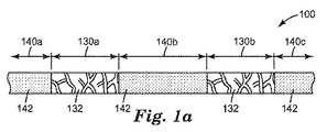
図1aは、可変屈折率光抽出層の断面立面図である。可変屈折率光抽出層100は、第1の材料132を含む第1の領域130a及び130b、並びに第2の材料142を含む第2の領域140a、140b及び140cを含む。
FIG. 1a is a sectional elevation view of a variable refractive index light extraction layer. The variable refractive index
第1の領域130a及び130b内に位置する第1の材料132は、任意の好適な材料であってもよく、任意の好適な方法により形成されてもよい。いくつかの実施形態では、第1の材料132は、低屈折率材料を含むことができる。例示的な低屈折率材料としては、例えば、本説明の他の箇所、及び2011年2月25日出願の米国特許出願第61/446740号、発明の名称「Front−Lit Reflective Display Device and Method of Front−Lighting Reflective Display」に説明される、ナノボイド化ポリマー材料を含む、ナノ多孔質材料を挙げることができる。他の実施形態では、低屈折率材料は、例えば、2012年3月30日に出願の米国特許出願第61/617,842号、発明の名称「Protective Coating for Low Index Material」に説明されるコーティングなどの、ヒュームドシリカ系低屈折コーティングであることができる。第1の領域のための材料の選択は、重量、耐久性、加工の要件(例えば、材料が硬化工程を必要とするかどうか)、多孔性、屈折率、又は(光学ヘイズ、透明度、及び透過率を含む)透過性などの、任意数の好適な因子を考慮することができる。低屈折率層がナノボイド化され、パターン化された低屈折率領域が小さくなるように設計されたいくつかの実施形態では、パターン化された低屈折率領域は、500nm程の大きさ、1μm程の大きさ、10μm程の大きさ、又は50μm程の大きさであってよい。
The
第2の領域140a、140b、及び140c内の第2の材料142は、任意の好適な材料であることができる。いくつかの実施形態では、第2の材料142は、ナノボイド化ポリマー材料ではない。第2の領域140a、140b、及び140cは、第1の領域130a及び130bとは異なる特性を有してもよく、例えば、第2の領域140a、140b、及び140cが、第1の領域130a及び130bよりも高い屈折率を有することができる。いくつかの実施形態では、これは、第1の材料132及び第2の材料142の異なる特性に起因してもよい。
The
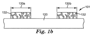
図1bは、低屈折率層の断面立面図である。低屈折率層101は、基材120、並びに第1の材料132を含んだ第1の領域130a及び130bを含む。基材120は、任意の好適な材料であってもよく、任意の好適な形状又はサイズであってもよい。図1bでは実質的に平面的なものとして示されるが、基材120は、いくつかの実施形態では、一次又は二次元に湾曲していることができる。いくつかの実施形態では、基材は環状であり、管状構造を形成することができる。基材120はまた、透明であってもよい。いくつかの実施形態では、基材120は、光導体であることができ、これは、基材が内部全反射(TIR)によって導波モード光を輸送することを意味する。光導体として、基材120はアクリル系光導体であってもよいし、又は基材120は、ポリカーボネート、ポリウレタン、又は任意の他の好適な材料から形成されてもよい。他の実施形態では、基材120は、ポリエチレンテレフタレート(PET)などのポリマーフィルムであることができる。基材120は、感圧接着剤を含む粘弾性光導体であってもよく、感圧接着剤は、適切な製造又は光学スタック内の隣接する層への接着を可能にすることができる。いくつかの実施形態では、基材120はまた、マイクロキャビティ化されポリエチレンテレフタレートなどの、反射性散乱要素であることができる。基材120は、その光学的特性、(反りに対する耐性若しくは可撓性などの)その物理的特性、又は任意のその他の好適な理由から選択できる。
FIG. 1b is a sectional elevation view of the low refractive index layer. The low
図1aに関連して説明されたように、第1の材料132は、低屈折率材料を含んでもよく、いくつかの場合には、第1の領域は、ナノボイド化ポリマー材料を含むことができる。第1の領域130a及び130bは、任意の好適な方法により基材120上に適用又はパターン化できる。いくつかの実施形態では、第1の領域130a及び130bは、基材上へ第1の材料132を選択的に印刷することによって、形成される。印刷としては、非インパクト式若しくはインパクト式印刷、又はデジタル若しくはアナログ印刷を挙げることができる。第1の領域130a及び130bは、フレキソ印刷により第1の材料132を選択的にパターン化することによって形成することができ、この場合には、低屈折率材料で充填された窪みを有するグラビアロールが、形状又はパターンの所望の配列を伴う刻印を有したフレキソ印刷ロールへ材料を転写させる。基材120の層が、刻印の上を通過して刻印と接触し、刻印が、第1の材料132を有したウェブを効果的に刻印又は印刷し、したがってフレキソ印刷ロールのパターンから基材120の面へ材料を転写させる。印刷としてはまた、輪転グラビア印刷、スクリーン印刷、インクジェット印刷、及びリソグラフ印刷を含む、他のプロセスを挙げることができる。熱転写、凹版、又はスプレー若しくはニードルダイコーティングが挙げられるがこれらに限定されない、選択的にパターン化する他の方法が、基材120上に第1の領域130a及び130bを作製する際に使用されてもよい。
As described in connection with FIG. 1a, the
いくつかの実施形態では、第1の領域130a及び130bは、第1の材料132の連続的な領域を堆積させ、次いで第1の材料の複数部を選択的に除去し、パターン化された第1の領域130a及び130bを残すことによって、形成される。第1の材料132の選択的な除去は、ウェットエッチング又はドライエッチング、反応性イオンエッチングと併用したフォトリソグラフィ、インプリント及びナノインプリントリソグラフィを含む、任意の好適な方法によって実行できる。
In some embodiments, the
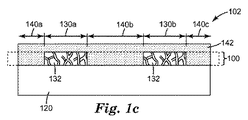
図1cは、図1bの低屈折率層に基づく別の可変屈折率光抽出層の断面立面図である。可変屈折率光抽出層102は、第1の材料132を含む第1の領域130a及び130b、並びに第2の材料142を含む第2の領域140a、140b及び140cを含む。可変屈折率領域100が強調され、第2の材料142のオーバーコーティングが、図1aに示されるように交互の第1及び第2の領域を作製できることを例示する。本説明では、「可変屈折率光抽出層」という用語は、交互の又はパターン化された第1及び第2の領域による領域を指すために使用され、領域が基材上にパターン化されるか否かは問わない。
FIG. 1c is a sectional elevation view of another variable index light extraction layer based on the low index layer of FIG. 1b. The variable refractive index
第2の材料142は、オーバーコートとして使用されるとき、任意好適な材料であってもよく、その物理的及び光学的特性により選択できる。いくつかの実施形態では、第2の材料142は、第1の材料132よりも高い屈折率を有することができる。第2の材料142はまた、溶融若しくはガラス転移温度、分子量、粘度、又は粘弾性などの、その物理的な特性により選択されてもよい。第2の材料142はまた、封止又は保護層としてのその特性により選択されてもよく、例えば、その透湿度、耐水性、又は耐引っかき性を考慮できる。いくつかの実施形態では、第2の材料142は、光学的に透明な接着剤若しくは感圧接着剤を含む粘弾性材料、高屈折率インク、ハードコート、ポリマー材料、又は硬化性樹脂であることができる。第2の材料142の屈折率は、光導体に連結されるときに所望の抽出効果を達成するために、選択又は修正されてもよい。いくつかの実施形態では、特に可変屈折率光抽出層102が光学スタックにおいて追加的なフィルムに取り付けられる場合に、第2の材料142が接着剤であることが有利であることができる。
The
第2の材料142は、他の箇所で述べられる印刷、パターン化、又はコーティングプロセスのうちのいずれかを含む、任意の好適な方法により低屈折率層上に適用されてもよい。第2の材料142はまた、低屈折率層上へ積層されてもよい。第2の材料142の粘度特性により、パターン化された第1の領域130a及び130bを有しなかった基材120上の区域に、すなわち、第2の領域140a、140b、及び140cにおよそ対応する第1の材料132の区域間に、材料を流し充填することが可能であることができる。
The
いくつかの実施形態では、第2の材料142は、基材とは反対の可変屈折率光抽出層の主面上に複数のマイクロ構造体を有することができる。複数のマイクロ構造体としては、レンズレット、プリズム、溝、又は任意の他の規則的若しくは不規則的な面構造を挙げることができる。いくつかの実施形態では、これらの複数のマイクロ構造体が、屈折により光を方向転換、再利用するか、又は転向させるために、形成又は選択できる。他の実施形態では、複数のマイクロ構造体は、回折により光を抽出するために、好適なサイズである。複数のマイクロ構造体は、エッチング、彫刻、エンボス加工、微細複製、並びにキャスト及び硬化プロセスを含む、任意の好適な方法によって形成できる。いくつかの実施形態では、回析又は屈折マイクロ構造体は、第2の材料142が適用されるのと同時に形成することができ、そのため可変屈折率光抽出層の製造を単純化し、その結果、複雑ではなく費用のかからないプロセスを提供できる。
In some embodiments, the
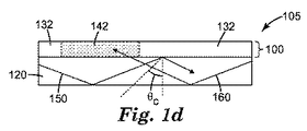
図1cの簡略化された図である図1dを参照すると、光線150及び160で表される光は、TIRによって隣接する層120内を輸送され続ける。この実施形態では、第1の材料132の屈折率は、示されるような臨界角θcを定める隣接する層の屈折率よりも、非常に低い屈折率となる。光線150で表される超臨界角で移動する光は、隣接する層120と第1の材料132との間の境界面に当たり、光線150のこの入射角はθcよりも大きく、その結果、境界面で反射し続ける光の実質的にすべてがもたらされる。
Referring to FIG. 1d, which is a simplified diagram of FIG. 1c, the light represented by
また、この実施形態では、第2の材料142の屈折率は、隣接する層120の屈折率とおよそ等しいか又は隣接する層120の屈折率よりも高い。この状況では、境界面に臨界角がなく、光線160で表される光は、隣接する層120と第2の材料142との間の境界面を通過し、したがって、隣接する層から層100内に抽出され続ける。
Also, in this embodiment, the refractive index of the
したがって、図1c及び図1dに示される実施形態に対しては、隣接する層において超臨界角で輸送され続ける光が、第1及び第2の領域の幾何学的配列に基づき、可変屈折率光抽出層によって選択的に抽出できるように、第1及び第2の領域は互いに対して配置される。いくつかの実施形態では、選択的な抽出は、例えば、一方の領域によるが他方の領域にはよらず、完全に又は部分的に抽出される光を含むことができる。可変屈折率光抽出層はまた、可変屈折率光抽出層の両側の上に2つの層又は光導体を含む、可変屈折率光抽出層に光学的に連結された2つ以上の層から光を抽出するように構成されることができる。いくつかの実施形態では、可変屈折率光抽出層は、2つ以上の側部から光を抽出するために、基材の2つ以上の側部に配置することができる。例えば、光導体として使用されるように設計された平面的な基材が、対向する主表面又は主面上に2つの可変屈折率抽出層を有することができる。別の例では、正方形の断面を有するロッドとして説明できる光導体が、その4つの主面上に可変光抽出層を有することができる。更に別の例では、円筒状のロッドである光導体が、その湾曲した表面を覆う可変光抽出層を有することができる。 Thus, for the embodiment shown in FIGS. 1c and 1d, the light that continues to be transported at supercritical angles in adjacent layers is based on the geometrical arrangement of the first and second regions, and the variable index light. The first and second regions are arranged relative to each other so that they can be selectively extracted by the extraction layer. In some embodiments, selective extraction can include, for example, light that is completely or partially extracted by one region but not the other. The variable index light extraction layer also includes light from two or more layers optically coupled to the variable index light extraction layer, including two layers or light guides on either side of the variable index light extraction layer. Can be configured to extract. In some embodiments, the variable index light extraction layer can be disposed on more than one side of the substrate to extract light from more than one side. For example, a planar substrate designed to be used as a light guide can have two variable refractive index extraction layers on opposing major surfaces or major surfaces. In another example, a light guide that can be described as a rod having a square cross-section can have a variable light extraction layer on its four major surfaces. In yet another example, the light guide, which is a cylindrical rod, can have a variable light extraction layer covering its curved surface.
図1eは、光が臨界角未満で隣接する層上に衝突している、光学フィルム105の概略断面図である。光線180及び190で表される光は、隣接する層120の表面170上に臨界角未満で衝突し、光は、層120及び100によって本質的に偏向することなく移動する。光線190で表される光は、第1の材料132を通過して移動し、光線180で表される光は第2の材料142を通過して移動する。可変屈折率光抽出層100の異なる領域を通過して移動する光の逸脱はほとんどない。これにより、低ヘイズ及び高透明度を有することができる、例示的な光学フィルム105などの、光学フィルムがもたらされ、その結果、この光学フィルムを介して見るとき、反対側の像の歪みはほとんどない。可変屈折率光抽出層は、所望の抽出された光パターンを生成するために、ランダム又は疑似ランダムな配列を含む、第1及び第2の領域の任意の幾何学的配列を有することができる。
FIG. 1e is a schematic cross-sectional view of the
一般に、可変屈折率光抽出層の屈折率分布は、層の所望の光学性能が得られる限り、どんな形で変化してもよい。図2は、層の横断面にわたって変化することができる屈折率を有する可変屈折率光抽出層を示す。屈折率分布は、平面視での層に対する、層の横断面にわたる距離に対応した、距離dのプロットを示す。図2は、d0に対応する層上のいずれかの初期位置で、層が、第1の領域に対応する第1の屈折率n1を有することを示す。層の横断面にわたって移動すると、層の屈折率が第2の領域の第2の屈折率に対応するn2へと急激に増加するd1に到達するまで、第1の屈折率n1が観察される。層の横断面にわたって移動し続けると、層の屈折率が第2の第1の領域を示すn1へ急激に減少するd2に到達するまで、第2の屈折率n2が観察される。 In general, the refractive index profile of the variable index light extraction layer may vary in any way as long as the desired optical performance of the layer is obtained. FIG. 2 shows a variable index light extraction layer having a refractive index that can vary across the cross section of the layer. The refractive index profile shows a plot of the distance d, corresponding to the distance across the cross section of the layer, for the layer in plan view. FIG. 2 shows that at any initial position on the layer corresponding to d 0 , the layer has a first refractive index n 1 corresponding to the first region. As it moves across the cross-section of the layer, the first refractive index n 1 is observed until it reaches d 1 where the refractive index of the layer increases rapidly to n 2 corresponding to the second refractive index of the second region. Is done. As it continues to move across the cross section of the layer, a second index of refraction n 2 is observed until it reaches d 2 where the index of refraction of the layer sharply decreases to n 1 representing the second first region.
低い及び高い屈折率をそれぞれ有した2つの隣接する第1及び第2の領域間の屈折率の変化は、多くの方法で変化することができる。例えば、屈折率の変化は、2つの隣接する領域間で、階段関数のように、急激であることができる。別の例に対しては、屈折率の変化は、単調であることができ、(第1の領域から第2の領域への又は第2の領域から第1の領域へのそれぞれの移動に応じて変化が観察されるかどうかに従い)屈折率は連続的に増加又は減少する。いくつかの場合には、隣接する第1及び第2の領域の第1及び第2屈折率は、階段及び単調関数のいくつかの組み合わせによって変化する。 The change in refractive index between two adjacent first and second regions having low and high refractive indices, respectively, can be varied in many ways. For example, the change in refractive index can be abrupt, like a step function, between two adjacent regions. For another example, the change in refractive index can be monotonic (in response to the respective movement from the first region to the second region or from the second region to the first region). The refractive index increases or decreases continuously (depending on whether a change is observed). In some cases, the first and second refractive indices of adjacent first and second regions vary with some combination of steps and monotonic functions.
可変光抽出層の第1の領域は、第2の領域の屈折率よりも低い屈折率を有する。例えば、第1の屈折率は、約1.4未満、約1.3未満、又は約1.2未満であることができる。第1の屈折率は、約1.15〜約1.45、約1.2〜約1.42、約1.2〜約1.40、又は約1.2〜約1.35であることができる。一般に、特定の第1及び第2の屈折率、並びに2つ屈折率間の特定の差は、以下に説明されるように可変屈折率光抽出層の所望の光学性能に左右される。第1及び第2の領域間の屈折率の差は、約0.03より大きい。いくつかの実施形態では、第1及び第2の領域間の屈折率の差は、0.05より大きく、0.1より大きく、0.2より大きく、又は0.25より大きい。 The first region of the variable light extraction layer has a refractive index lower than that of the second region. For example, the first refractive index can be less than about 1.4, less than about 1.3, or less than about 1.2. The first refractive index is about 1.15 to about 1.45, about 1.2 to about 1.42, about 1.2 to about 1.40, or about 1.2 to about 1.35. Can do. In general, the specific first and second refractive indices and the specific difference between the two refractive indices will depend on the desired optical performance of the variable refractive index light extraction layer as described below. The difference in refractive index between the first and second regions is greater than about 0.03. In some embodiments, the difference in refractive index between the first and second regions is greater than 0.05, greater than 0.1, greater than 0.2, or greater than 0.25.
ナノボイド化ポリマー材料は、結合剤内に分散した、複数の相互接続されたナノボイド又はナノボイドの網目構造を典型的に含む。複数の又は網目構造のナノボイドのうちの少なくとも一部は、中空トンネル又は中空トンネル様通路を介して、互いに接続される。ナノボイドは、必ずしもあらゆる物質及び/又は微粒子を含まないとは限らない。例えば、いくつかの場合には、ナノボイドは、例えば結合剤及び/又はナノ粒子を含む、1つ又は複数の小さな繊維様物体又はひも様物体を含むことができる。いくつかの開示された第1の領域は、それぞれの複数の又は網目構造のナノボイドが相互接続された、多重多数の相互接続されたナノボイド、又はナノボイドの多重網目構造を含む。いくつかの場合には、多重多数の相互接続されたナノボイドに加えて、開示された第1の領域は、ナノボイドがトンネルを介して他のナノボイドに接続されないことを意味する、閉じた又は非接続ナノボイドを僅かに含むことができる。 Nanovoided polymeric materials typically comprise a plurality of interconnected nanovoids or a network of nanovoids dispersed within a binder. At least some of the plurality or network of nanovoids are connected to each other via a hollow tunnel or a hollow tunnel-like passage. Nanovoids do not necessarily include all substances and / or microparticles. For example, in some cases, nanovoids can include one or more small fiber-like or string-like objects including, for example, binders and / or nanoparticles. Some disclosed first regions include multiple multiple interconnected nanovoids, or nanovoid multi-networks, each interconnected with a plurality or network of nanovoids. In some cases, in addition to multiple interconnected nanovoids, the disclosed first region is closed or disconnected, meaning that the nanovoids are not connected to other nanovoids through the tunnel A slight amount of nanovoids can be contained.
ナノボイド化ポリマー材料は、複数のナノボイドを含むことによりTIRを支援するように設計される。光学的に透明な(清澄及び非多孔質な)隣接する層内を移動する光が、高い多孔性を有する層に入射するとき、入射光の反射率は、垂直入射よりも、斜角で非常に高い。ほとんどヘイズを有しないナノボイド化された第1の領域の場合には、臨界角よりも大きい傾斜角での反射率は約100%に近い。このような場合に、入射光はTIRする。 Nanovoided polymeric materials are designed to support TIR by including multiple nanovoids. When light traveling in an optically transparent (clear and non-porous) adjacent layer is incident on a layer with high porosity, the reflectivity of the incident light is much more oblique and more oblique than normal incidence. Very expensive. In the case of the nanovoided first region having almost no haze, the reflectivity at an inclination angle larger than the critical angle is close to about 100%. In such a case, the incident light undergoes TIR.
開示された第1の領域内のナノボイドは、屈折率nv及び誘電率εvを有し、nv 2=εvであり、結合剤は、屈折率nb及び誘電率εbを有し、nb 2=εbである。一般に、ナノボイド化ポリマー材料の層と、層に入射するか又は層内を伝播する光などの、光との相互作用は、例えば、層の厚さ、結合剤の屈折率、ナノボイド又は細孔の屈折率、細孔の形状及びサイズ、細孔の空間分布、並びに光の波長などの、層の多くの特性に左右される。いくつかの場合には、ナノボイド化ポリマー材料の層に入射するか又はナノボイド化ポリマー材料の層内を伝播する光は、有効誘電率εeff及び有効屈折率neff「に出会う」か又は「を経験し」、この場合、neffは、ナノボイドの屈折率nv、結合剤の屈折率nb、及びナノボイドの多孔性又は体積分率「f」によって表わすことができる。このような場合、光が、単一、つまり独立したナノボイドの形状及び形体を解像することができないように、層は十分に厚く、ナノボイドは十分に小さい。このような場合、ナノボイドの少なくとも60%、又は70%、又は80%、又は90%といった、少なくとも大多数のナノボイドのサイズは、約λ/5以下、又は約λ/6以下、又は約λ/8以下、又は約λ/10以下、又は約λ/20以下であり、ここでλは光の波長である。 The disclosed nanovoids in the first region have a refractive index n v and a dielectric constant ε v and n v 2 = ε v and the binder has a refractive index n b and a dielectric constant ε b , N b 2 = ε b . In general, the interaction of a layer of nanovoided polymeric material with light, such as light incident on or propagating in the layer, is, for example, the thickness of the layer, the refractive index of the binder, the nanovoids or pores. It depends on many properties of the layer, such as refractive index, pore shape and size, pore spatial distribution, and light wavelength. In some cases, light incident on or propagating through a layer of nanovoided polymeric material may “see” the effective dielectric constant ε eff and the effective refractive index n eff. Experienced, where n eff can be represented by the refractive index n v of the nanovoid, the refractive index n b of the binder, and the porosity or volume fraction “f” of the nanovoid. In such a case, the layers are sufficiently thick and the nanovoids are small enough so that light cannot resolve the single, i.e., independent, nanovoid shape and shape. In such cases, the size of at least the majority of the nanovoids, such as at least 60%, or 70%, or 80%, or 90% of the nanovoids is about λ / 5 or less, or about λ / 6 or less, or about λ / 8 or less, or about λ / 10 or less, or about λ / 20 or less, where λ is the wavelength of light.
いくつかの実施形態では、可変光抽出層の開示された第1の領域に入射する光は、約380nm〜約750nm、又は約400nm〜約700nm、又は約420nm〜約680nmの範囲内であることができる可視光である。このような場合、ナノボイドの少なくとも60%、又は70%、又は80%、又は90%といった、少なくとも大多数のナノボイドのサイズが、約70nm以下、又は約60nm以下、又は約50nm以下、又は約40nm以下、又は約30nm以下、又は約20nm以下、又は約10nm以下である場合には、可変光抽出層の第1の領域は、有効屈折率を有し、複数のナノボイドを含む。 In some embodiments, the light incident on the disclosed first region of the variable light extraction layer is in the range of about 380 nm to about 750 nm, or about 400 nm to about 700 nm, or about 420 nm to about 680 nm. Visible light. In such cases, the size of at least the majority of the nanovoids, such as at least 60%, or 70%, or 80%, or 90% of the nanovoids, is about 70 nm or less, or about 60 nm or less, or about 50 nm or less, or about 40 nm. The first region of the variable light extraction layer has an effective refractive index and includes a plurality of nanovoids if less than or about 30 nm, or less than about 20 nm, or less than about 10 nm.
いくつかの場合には、領域が、ナノボイド及び結合剤の屈折率、並びにナノボイド又は細孔の体積分率又は多孔率によって表わすことができる有効屈折率を合理的に有することができるように、可変屈折率光抽出層の開示された第1の領域は十分に厚い。このような場合、第1の領域の厚さは、約100nm以上、又は約200nm以上、又は約500nm以上、又は約700nm以上、又は約1000nm以上である。 In some cases, the region is variable so that it can reasonably have an effective refractive index that can be represented by the refractive index of the nanovoids and binder, and the volume fraction or porosity of the nanovoids or pores. The disclosed first region of the refractive index light extraction layer is sufficiently thick. In such cases, the thickness of the first region is about 100 nm or more, or about 200 nm or more, or about 500 nm or more, or about 700 nm or more, or about 1000 nm or more.
開示された第1の領域内のナノボイドが十分に小さく、領域が十分に厚いとき、第1の領域は、以下のように表わすことができる有効誘電率εeffを有する。
εeff=f εv+(1−f)εb (1)
When the nanovoids in the disclosed first region are small enough and the region is thick enough, the first region has an effective dielectric constant ε eff that can be expressed as:
ε eff = f ε v + (1−f) ε b (1)
このような場合、第1の領域の有効屈折率neffは、以下のように表わすことができる。
neff 2=f nv 2+(1−f)nb 2 (2)
In such a case, the effective refractive index n eff of the first region can be expressed as follows.
n eff 2 = f n v 2 + (1−f) n b 2 (2)
細孔の屈折率と結合剤の屈折率との差が十分に小さいときなどの、いくつかの場合には、第1の領域の有効屈折率は、以下の式で近似できる。
neff=f nv+(1−f)nb (3)
In some cases, such as when the difference between the refractive index of the pores and the refractive index of the binder is sufficiently small, the effective refractive index of the first region can be approximated by:
n eff = f n v + (1−f) n b (3)
このような場合、第1の領域の有効屈折率は、ナノボイドの屈折率と結合剤の屈折率の体積加重平均である。例えば、約50%のボイドの体積分率を有する第1の領域及び約1.5の屈折率を有する結合剤は、約1.25の有効屈折率を有する。 In such a case, the effective refractive index of the first region is a volume weighted average of the refractive index of the nanovoid and the refractive index of the binder. For example, a first region having a void volume fraction of about 50% and a binder having a refractive index of about 1.5 has an effective refractive index of about 1.25.
図3は、結合剤内に実質的に均一に分散した、ナノボイドの網目構造又は複数の相互接続されたナノボイド、及び複数の粒子を含む、可変屈折率光抽出層の第1の領域の概略断面図である。第1の領域300は、結合剤310内に分散した複数の相互接続されたナノボイド320を含む。ナノボイド320は、相互接続されたナノボイド320A〜320Cを含む。第1及び第2の主要表面330及び332は、それぞれ、一方の表面から別の表面へ、又は領域の厚みを貫いて延在するトンネルを提供しても又は提供しなくてもよい表面細孔320D〜Gによって示されるように、多孔性である。ナノボイド320B及び320Cなどの、ナノボイドの一部は、第1の領域の内部にあり、表面へトンネルを作っても又作らなくてもよい。
FIG. 3 is a schematic cross section of a first region of a variable refractive index light extraction layer comprising a nanovoid network or a plurality of interconnected nanovoids and a plurality of particles substantially uniformly dispersed within a binder. FIG. The
ボイド320は、好適な組成物を、並びにコーティング、乾燥及び硬化などの製造条件を、選択することによって一般に制御できるサイズd1を有する。一般に、d1は、任意の所望の数値範囲内の任意の所望の値であることができる。例えば、いくつかの場合には、ナノボイドの少なくとも60%、又は70%、又は80%、又は90%、又は95%といった、少なくとも大多数のナノボイドが、所望の範囲内にあるサイズを有する。例えば、いくつかの場合には、ナノボイドの少なくとも60%、又は70%、又は80%、又は90%、又は95%といった、少なくとも大多数のナノボイドが、約500nm以下、又は400nm以下、又は約300nm以下、又は約200nm以下、又は約100nm以下、又は約70nm以下、又は約50nm以下のサイズを有する。いくつかの場合には、ほとんど又はまったく光の散乱なしに、領域の屈折率が変化するように、ナノボイドの一部は十分に小さいことができる。
結合剤310は、ポリマーなどの任意の材料を含むことができる。結合剤は、モノマーを含む重合性組成物から形成されたポリマーであってもよく、この場合、モノマーは、例えば、可視光、紫外線照射、電子ビーム照射などの化学線照射の使用、熱、及びこれらの組み合わせの使用、又は化学的に若しくは熱的に開始できる種々の従来のアニオン性、カチオン性、フリーラジカル性、若しくはその他の重合技術のうちのいずれかを使用して、硬化することがされる。重合は、溶媒重合、乳化重合、懸濁重合、バルク重合などを使用して実施できる。有用なモノマーには、約500g/モル未満の分子量を有した小分子、500g/モルより大きく約10,000g/モルまでの分子量を有したオリゴマー、及び10,000g/モルより大きく約100,000g/モルまでの分子量を有したポリマーが含まれる。
The
本開示の実施に好適な硬化性基の代表的な例としては、エポキシ基、エチレン性不飽和基、オレフィン炭素−炭素二重結合、アリルオキシ基、(メタ)アクリレート基、(メタ)アクリルアミド基、シアノエステル基、ビニルエーテル基、これらの組み合わせなどが挙げられる。モノマーは、単官能性又は多官能性であってもよく、重合の際に架橋された網目構造を形成することが可能であることができる。本明細書で使用するとき、(メタ)アクリレートはアクリレート及びメタクリレートを指し、(メタ)アクリルアミドはアクリルアミド及びメタクリルアミドを指す。 Representative examples of curable groups suitable for the practice of this disclosure include epoxy groups, ethylenically unsaturated groups, olefinic carbon-carbon double bonds, allyloxy groups, (meth) acrylate groups, (meth) acrylamide groups, Examples thereof include a cyanoester group, a vinyl ether group, and combinations thereof. Monomers can be monofunctional or polyfunctional and can be capable of forming a crosslinked network upon polymerization. As used herein, (meth) acrylate refers to acrylate and methacrylate, and (meth) acrylamide refers to acrylamide and methacrylamide.
有用なモノマーとしては、スチレン、α−メチルスチレン、置換スチレン、ビニルエステル、ビニルエーテル、N−ビニル−2−ピロリドン、(メタ)アクリルアミド、N−置換(メタ)アクリルアミド、オクチル(メタ)アクリレート、イソ−オクチル(メタ)アクリレート、ノニルフェノールエトキシレート(メタ)アクリレート、イソノニル(メタ)アクリレート、ジエチレングリコール(メタ)アクリレート、イソボルニル(メタ)アクリレート、2−(2−エトキシエトキシ)エチル(メタ)アクリレート、2−エチルヘキシル(メタ)アクリレート、ラウリル(メタ)アクリレート、ブタンエジオールモノ(メタ)アクリレート、ベータ−カルボキシエチル(メタ)アクリレート、イソブチル(メタ)アクリレート、脂環式エポキシド、α−エポキシド、2−ヒドロキシエチル(メタ)アクリレート、(メタ)アクリロニトリル、無水マレイン酸、イタコン酸、イソデシル(メタ)アクリレート、ドデシル(メタ)アクリレート、n−ブチル(メタ)アクリレート、メチル(メタ)アクリレート、ヘキシル(メタ)アクリレート、(メタ)アクリル酸、N−ビニルカプロラクタム、ステアリル(メタ)アクリレート、ヒドロキシ官能ポリカプロラクトンエステル(メタ)アクリレート、ヒドロキシエチル(メタ)アクリレート、ヒドロキシメチル(メタ)アクリレート、ヒドロキシプロピル(メタ)アクリレート、ヒドロキシイソプロピル(メタ)アクリレート、ヒドロキシブチル(メタ)アクリレート、ヒドロキシイソブチル(メタ)アクリレート、テトラヒドロフルフリル(メタ)アクリレート、これらの組み合わせなどが挙げられる。 Useful monomers include styrene, α-methylstyrene, substituted styrene, vinyl ester, vinyl ether, N-vinyl-2-pyrrolidone, (meth) acrylamide, N-substituted (meth) acrylamide, octyl (meth) acrylate, iso- Octyl (meth) acrylate, nonylphenol ethoxylate (meth) acrylate, isononyl (meth) acrylate, diethylene glycol (meth) acrylate, isobornyl (meth) acrylate, 2- (2-ethoxyethoxy) ethyl (meth) acrylate, 2-ethylhexyl ( (Meth) acrylate, lauryl (meth) acrylate, butaneediol mono (meth) acrylate, beta-carboxyethyl (meth) acrylate, isobutyl (meth) acrylate, alicyclic epoxy Sid, α-epoxide, 2-hydroxyethyl (meth) acrylate, (meth) acrylonitrile, maleic anhydride, itaconic acid, isodecyl (meth) acrylate, dodecyl (meth) acrylate, n-butyl (meth) acrylate, methyl (meth) ) Acrylate, hexyl (meth) acrylate, (meth) acrylic acid, N-vinylcaprolactam, stearyl (meth) acrylate, hydroxy-functional polycaprolactone ester (meth) acrylate, hydroxyethyl (meth) acrylate, hydroxymethyl (meth) acrylate, Hydroxypropyl (meth) acrylate, hydroxyisopropyl (meth) acrylate, hydroxybutyl (meth) acrylate, hydroxyisobutyl (meth) acrylate, tetrahydrofur Lil (meth) acrylate, combinations thereof, and the like.
官能性オリゴマー及びポリマーはまた、本明細書において「高分子量の成分又は種」と総称される場合がある。好適な高分子量の成分が、本開示の組成物に組み込むことができる。このような高分子量の成分は、粘度制御、硬化の際の低減した収縮、耐久性、可撓性、多孔性及び非多孔性基材への接着、屋外耐候性、及び/又は同様のものといった、利点を提供することができる。本開示の流体組成物に組み込まれるオリゴマー及び/又はポリマーの量は、結果として得られる組成物の用途、反応性希釈剤の性質、オリゴマー及び/又はポリマーの性質及び重量平均分子量などの要因に応じて、広範囲内で変化することができる。オリゴマー及び/又はポリマー自体は、直鎖状、分枝状、及び/又は環状であってもよい。分枝状オリゴマー及び/又はポリマーは、同等の分子量の直鎖状オリゴマー及び/又はポリマーよりも低い粘度を有する傾向にある。 Functional oligomers and polymers may also be collectively referred to herein as “high molecular weight components or species”. Any suitable high molecular weight component can be incorporated into the compositions of the present disclosure. Such high molecular weight components include viscosity control, reduced shrinkage upon curing, durability, flexibility, adhesion to porous and non-porous substrates, outdoor weather resistance, and / or the like Can provide benefits. The amount of oligomer and / or polymer incorporated into the fluid composition of the present disclosure depends on factors such as the use of the resulting composition, the nature of the reactive diluent, the nature of the oligomer and / or polymer and the weight average molecular weight. Can vary within a wide range. The oligomer and / or polymer itself may be linear, branched and / or cyclic. Branched oligomers and / or polymers tend to have lower viscosities than linear oligomers and / or polymers of comparable molecular weight.
例示的な重合性オリゴマー又はポリマーとしては、脂肪族ポリウレタン、アクリル、ポリエステル、ポリイミド、ポリアミド、エポキシポリマー、(スチレンのコポリマーを含む)ポリスチレン及び置換スチレン、シリコーン含有ポリマー、フッ素化ポリマー、これらの組み合わせなどが挙げられる。いくつかの用途に対して、ポリウレタン及びアクリレートオリゴマー及び/又はポリマーは、改善した耐久性及び耐候性特性を有することができる。このような材料はまた、放射線硬化性(メタ)アクリレート官能性モノマーから形成された反応性希釈剤に容易に溶解できる傾向にある。 Exemplary polymerizable oligomers or polymers include aliphatic polyurethanes, acrylics, polyesters, polyimides, polyamides, epoxy polymers, polystyrene and substituted styrenes (including copolymers of styrene), silicone-containing polymers, fluorinated polymers, combinations thereof, and the like Is mentioned. For some applications, polyurethane and acrylate oligomers and / or polymers can have improved durability and weathering properties. Such materials also tend to be readily soluble in reactive diluents formed from radiation curable (meth) acrylate functional monomers.
オリゴマー及び/又はポリマーの芳香族成分は、一般に、乏しい耐候性、及び/又は太陽光に対して乏しい抵抗力を有する傾向にあるので、芳香族成分は、5重量パーセント未満、好ましくは1重量パーセント未満に限定され得、本開示のオリゴマー及び/又はポリマー並びに反応性希釈剤から実質的に除外できる。したがって、直鎖状、分枝状及び/又は環状脂肪族及び/又は複素環式成分が、屋外用途で使用されるオリゴマー及び/又はポリマーを形成するのに好ましい。 Since aromatic components of oligomers and / or polymers generally tend to have poor weather resistance and / or poor resistance to sunlight, aromatic components are less than 5 weight percent, preferably 1 weight percent. And can be substantially excluded from the oligomers and / or polymers and reactive diluents of the present disclosure. Accordingly, linear, branched and / or cycloaliphatic and / or heterocyclic components are preferred to form oligomers and / or polymers used in outdoor applications.
本開示で使用するために好適な放射線硬化性オリゴマー及び/又はポリマーとしては、(メタ)アクリル化ウレタン(すなわちウレタン(メタ)アクリレート)、(メタ)アクリル化エポキシ(すなわちエポキシ(メタ)アクリレート)、(メタ)アクリル化ポリエステル(すなわちポリエステル(メタ)アクリレート)、(メタ)アクリル化(メタ)アクリル、(メタ)アクリル化シリコーン、(メタ)アクリル化ポリエーテル(すなわちポリエーテル(メタ)アクリレート)、ビニル(メタ)アクリレート、及び(メタ)アクリル化オイルが挙げられるが、これらに限定されない。 Suitable radiation curable oligomers and / or polymers for use in the present disclosure include (meth) acrylated urethane (ie urethane (meth) acrylate), (meth) acrylated epoxy (ie epoxy (meth) acrylate), (Meth) acrylated polyester (ie polyester (meth) acrylate), (meth) acrylated (meth) acrylic, (meth) acrylated silicone, (meth) acrylated polyether (ie polyether (meth) acrylate), vinyl Although (meth) acrylate and (meth) acrylated oil are mentioned, it is not limited to these.
ナノボイド化層300を強化するために有用である材料としては、高い引張強度及び高い伸度を有する樹脂、例えば、ペンシルベニア州エクストンのSartomer社から市販されるCN9893、CN902、CN9001、CN961、及びCN964;並びにニュージャージー州ウッドランドパークのCytecから市販されるEBECRYL 4833及びEb8804が挙げられる。好適な強化材料はまた、「硬質」オリゴマーアクリレートと「軟質」オリゴマーアクリレートとの組み合わせを含む。「硬質」アクリレートの例としては、(Cytecから市販の)EBECRYL 4866などのポリウレタンアクリレート、EBECRYL 838などのポリエステルアクリレート、並びにEBECRYL 600、EBECRYL 3200、及びEBECRYL 1608などの、エポキシアクリレート;並びに、(Sartomer社から市販の)CN2920、CN2261、及びCN9013が挙げられる。「軟質」アクリレートの例としては、Cytecから市販されるEBECRYL 8411;並びにSartomer社から市販されるCN959、CN9782、及びCN973が挙げられる。これらの材料は、総固形分(溶媒画分を除く)の5〜25重量%の範囲でコーティング配合物に添加されるときに、ナノボイド化構造化層の強化に有効である。
Materials that are useful for reinforcing the
ナノボイド化ポリマー材料は、粒子を含有しても又は含有しなくてもよい。粒子340は、任意の所望の数値範囲内の任意の所望の値であることができるサイズd2を有する。例えば、いくつかの場合には、粒子の少なくとも60%、又は70%、又は80%、又は90%、又は95%といった、少なくとも大多数の粒子が、所望の範囲内にあるサイズを有する。例えば、いくつかの場合には、粒子の少なくとも60%、又は70%、又は80%、又は90%、又は95%といった、少なくとも大多数の粒子が、約5μm以下、又は3μm以下、又は約2μm以下、又は約1ミクロン以下、又は約700nm以下、又は約500nm以下、又は約200nm以下、又は約100nm以下、又は約50nm以下のサイズを有する。
The nanovoided polymeric material may or may not contain particles.
いくつかの場合には、粒子340は、約5μm以下、又は約3μm以下、又は約2μm以下、又は約1μm以下、又は約700nm以下、又は約500nm以下、又は約200nm以下、又は約100nm以下、又は約50nm以下の平均粒径を有する。いくつかの場合には、ほとんど又はまったく光の散乱なしに、領域の屈折率が変化するように、粒子の一部が十分に小さくなることができる。
In some cases, the
いくつかの場合には、ほとんど又はまったく光の散乱なしに、領域の屈折率が変化するように、d1及び/又はd2が十分に小さくなる。このような場合、例えば、d1及び/又はd2は、約λ/5以下、又は約λ/6以下、又は約λ/8以下、又は約λ/10以下、又は約λ/20以下であり、ここでλは光の波長である。別の例としては、このような場合、d1及びd2は、約70nm以下、又は約60nm以下、又は約50nm以下、又は約40nm以下、又は約30nm以下、又は約20nm以下、又は約10nmである。 In some cases, d 1 and / or d 2 are sufficiently small so that the refractive index of the region changes with little or no light scattering. In such cases, for example, d 1 and / or d 2 is about λ / 5 or less, or about λ / 6 or less, or about λ / 8 or less, or about λ / 10 or less, or about λ / 20 or less. Where λ is the wavelength of the light. As another example, in such cases, d 1 and d 2 are about 70 nm or less, or about 60 nm or less, or about 50 nm or less, or about 40 nm or less, or about 30 nm or less, or about 20 nm or less, or about 10 nm. It is.
ナノボイド化ポリマー層で使用される粒子の他の特性としては、形状が挙げられる。粒子は、球形などの規則的な形状、又は不規則な形状を有することができる。粒子は、約1.5以上、又は約2以上、又は約3以上、又は約4以上、又は約5以上の平均アスペクト比を有して細長いことができる。いくつかの場合には、粒子は、(テキサス州ヒューストンのNissan Chemical USAから入手可能なSNOWTEX−PS粒子などの)真珠の首飾りの形態若しくは形状、又はヒュームドシリカなどの球形若しくは非晶質粒子の凝集した連鎖であることができる。 Another property of the particles used in the nanovoided polymer layer includes shape. The particles can have a regular shape, such as a sphere, or an irregular shape. The particles can be elongated with an average aspect ratio of about 1.5 or higher, or about 2 or higher, or about 3 or higher, or about 4 or higher, or about 5 or higher. In some cases, the particles are in the form or shape of a pearl necklace (such as SNOWTX-PS particles available from Nissan Chemical USA, Houston, Texas), or spherical or amorphous particles such as fumed silica. It can be an agglomerated chain.
ナノ粒子は、無機若しくは有機、又はこれらの組み合わせであることができる。いくつかの実施形態では、ナノ粒子は、多孔性粒子、中空粒子、中実粒子、又はこれらの組み合わせであることができる。好適な無機ナノ粒子の例としては、シリカ、並びにジルコニア、チタニア、セリア、アルミナ、酸化鉄、バナジア、酸化アンチモン、酸化スズ、アルミナ/シリカ、シリカ/ジルコニア、及びこれらの組み合わせなどの、金属酸化物が挙げられる。ナノ粒子は、ナノ粒子が結合剤に化学的及び/又は物理的に結合するように、表面修飾することができる。化学的結合の場合、表面修飾されたナノ粒子は、結合剤と化学的に反応する官能性を有する。一般に、表面修飾は、周知であり、先に引用された参照文献で説明されたような従来の材料及び技術を用いて実施できる。 The nanoparticles can be inorganic or organic, or a combination thereof. In some embodiments, the nanoparticles can be porous particles, hollow particles, solid particles, or combinations thereof. Examples of suitable inorganic nanoparticles include silica and metal oxides such as zirconia, titania, ceria, alumina, iron oxide, vanadia, antimony oxide, tin oxide, alumina / silica, silica / zirconia, and combinations thereof. Is mentioned. The nanoparticles can be surface modified such that the nanoparticles are chemically and / or physically bound to the binder. In the case of chemical bonding, the surface-modified nanoparticles have a functionality that chemically reacts with the binder. In general, surface modifications are well known and can be performed using conventional materials and techniques as described in the previously cited references.
結合剤とナノ粒子との重量比は、ナノボイド化ポリマー層の所望の特性に応じて、約30:70、40:60、50:50、55:45、60:40、70:30、80:20、又は90:10以上の範囲であることができる。ナノ粒子の重量%の好ましい範囲は、約10重量%〜約60重量%の範囲であり、使用されるナノ粒子の密度及び寸法に左右できる。 The weight ratio of binder to nanoparticles is about 30:70, 40:60, 50:50, 55:45, 60:40, 70:30, 80: depending on the desired properties of the nanovoided polymer layer. It can be in the range of 20, or 90:10 or more. A preferred range of weight percent of nanoparticles is in the range of about 10% to about 60% by weight and can depend on the density and size of the nanoparticles used.
ボイド320の網目構造及び粒子340の主な光学的効果が、有効屈折率に影響を及ぼすこと、及び散乱光を最小化することである場合には、ボイド320及び粒子340による光学層300の光学ヘイズは、約5%以下、又は約4%以下、又は約3.5%以下、又は約4%以下、又は約3%以下、又は約2.5%以下、又は約2%以下、又は約1.5%以下、又は約1%以下である。このような場合、光学層の有効媒質の有効屈折率は、約1.40以下、又は約1.35以下、又は約1.3以下、又は約1.25以下、又は約1.2以下、又は約1.15以下である。
If the main optical effect of the void 320 network and the
第1の領域300は、結合剤310及び粒子340に加えて、他の材料を有してもよい。例えば、第1の領域300は、ナノボイド化ポリマー材料が形成されている、基材の表面を湿潤させるのを助けるために、図3には明確に示されていないが、例えばカップリング剤などの1つ又は複数の添加剤を含むことができる。第1の領域300中の他の例示的な材料としては、1つ又は複数の光開始剤などの反応開始剤、帯電防止剤、紫外線吸収剤、及び剥離剤が挙げられる。
The
ナノボイド化ポリマー材料は、パターン化されるかどうかを問わず、層として典型的に形成される。ナノボイド化ポリマー材料の層を作製する方法は、例えば、国際公開第2010/120422(A1)号(Kolbら)及び同第2010/120468(A1)号(Kolbら)に説明される。一プロセスでは、最初に、溶媒に溶解されたナノ粒子などの複数の粒子及び重合性材料を含む溶液が調製され、こ場合、重合性材料は、例えば1つ又は複数のタイプのモノマーを含むことができる。次に、重合性材料が、例えば、熱又は光を適用することによって重合され、溶媒中に不溶性ポリマーマトリックスを形成する。いくつかの場合には、重合工程後、溶媒が重合性材料の一部を依然として含んでもよいが、低濃度である。次に、溶液を乾燥又は蒸発させることによって溶媒が除去され、ポリマー結合剤310内に分散したボイド320の網目構造又は複数のボイド320を含む第1の領域300がもたらされる。第1の領域は更に、ポリマー内に分散した複数の粒子340を含む。粒子は結合剤に結合され、この結合は物理的又は化学的であることができる。
Nanovoided polymeric materials are typically formed as layers, whether patterned or not. Methods for making layers of nanovoided polymeric materials are described, for example, in WO 2010/120422 (A1) (Kolb et al.) And 2010/120468 (A1) (Kolb et al.). In one process, a solution is first prepared comprising a plurality of particles, such as nanoparticles dissolved in a solvent, and a polymerizable material, where the polymerizable material includes, for example, one or more types of monomers. Can do. The polymerizable material is then polymerized, for example, by applying heat or light, to form an insoluble polymer matrix in the solvent. In some cases, after the polymerization step, the solvent may still contain some of the polymerizable material, but at a low concentration. The solvent is then removed by drying or evaporating the solution, resulting in a
一般に、ナノボイド化ポリマー層は、所望の多孔率又はボイド体積で形成されることができ、多孔率又はボイド体積は、可変屈折率光抽出層の第1の領域の所望の特性を左右することができる。例えば、第1の領域は、約20%〜約70%、約30%〜約70%、又は約40%〜約70%のボイド体積を有することができる。いくつかの場合には、ボイド体積は、約20%以上、又は約30%以上、又は約40%以上、又は約50%以上、又は約60%以上、又は約70%以上、又は約80%以上、又は約90%以上である。 In general, the nanovoided polymer layer can be formed with a desired porosity or void volume, which can affect the desired properties of the first region of the variable index light extraction layer. it can. For example, the first region can have a void volume of about 20% to about 70%, about 30% to about 70%, or about 40% to about 70%. In some cases, the void volume is about 20% or more, or about 30% or more, or about 40% or more, or about 50% or more, or about 60% or more, or about 70% or more, or about 80%. Or about 90% or more.
いくつかの実施形態では、第1の領域300は、低い光学ヘイズを有する。このような場合、光学層の光学ヘイズは、約10%以下、又は約7%以下、又は約5%以下、又は約4%以下、又は約3.5%以下、又は約4%以下、又は約3%以下、又は約2.5%以下、又は約2%以下、又は約1.5%以下、又は約1%以下である。第1の領域にわたるヘイズ変化は、約1%〜5%、約1%〜3%、約1%〜2%、又は1%未満の範囲であることができる。このような場合、光学フィルムは、約1.40以下、又は約1.35以下、又は約1.3以下、又は約1.2以下、又は約1.15以下、又は約1.1以下、又は約1.05以下である低減した有効屈折率を有することができる。光学層300に垂直に入射する光に対して、光学ヘイズは、本明細書で使用するとき、垂直方向から4度を超えるまで偏向する透過光と全透過光との比と定義される。本明細書において開示されるヘイズ値は、ASTM D1003に説明される手順に従い、HAZE−GARD PLUSヘイズメーター(BYK−Gardiner、メリーランド州シルバースプリング)を使用して測定された。
In some embodiments, the
いくつかの実施形態では、第1の領域300は、高い光学的透明度を有する。光学層300に垂直に入射する光に対して、光学的透明度は、本明細書で使用するとき、比(T1−T2)/(T1+T2)を指し、ここで、T1は垂直方向から1.6度と2度との間で偏向する透過光であり、T2は垂直方向から0度と0.7度との間にある透過光である。本明細書において開示される透明度値は、BYK−Gardinerから入手したHAZE−GARD PLUSヘイズメーターを使用して測定された。第1の領域300が高い光学的透明度を有する場合には、透明度は、約80%以上、又は約85%以上、又は約90%以上、又は約95%以上である。
In some embodiments, the
第1の領域300のナノボイド化ポリマー材料は、基材上へ先に説明された溶媒含有溶液をコーティング又はパターン化することによって、作製できる。多くの場合、基材は、ロールツーロールプロセスにおいて有用な任意のポリマー材料で形成できる。いくつかの実施形態では、基材層は、ほとんど又はまったくヘイズを有せず高い透明度を有する透明性であり、ポリエチレンテレフタレート(PET)、ポリカーボネート、アクリル、及びシクロオレフィンポリマーなどの、ポリマーで形成される。基材はまた、ガラス及び他の透明な無機材料などの、透明な基材を含んでもよい。基材はまた、拡散白色ポリマー基材、多層光学フィルム(例えば3Mから入手可能なESR)などの半鏡面基材ポリマー基材、金属半鏡面反射体、例えばツヤ消しアルミニウムなどの、反射性散乱基材又は材料を含んでもよい。いくつかの場合には、ナノボイド化ポリマー層300が別の基材、例えば接着層へ転写することができるように、基材は剥離ライナーを含むことができる。
The nanovoided polymeric material of the
第1及び第2の領域は、所望の方法で光を調整するために、可変屈折率光抽出層の横断面にわたり、互いに対して配置できる。例えば、第2の領域は、層の横断面にわたりパターンで配列された複数の第2の領域を含むことができる。別の例としては、第2の領域は、層の横断面にわたりランダムに配列された複数の第2の領域を含むことができる。第1又は第2の領域のどちらかが、層の横断面にわたる連続的な領域であってもよい。非連続的、すなわち複数の領域である第1又は第2の領域のために、密度が、層の横断面にわたる任意の方向で変化してもよい。例えば、第2の領域の密度が、層の横断面にわたり一次元又は二次元で変化することができる。これらの実施形態のうちのいくつかは、図4a〜4d、図5a、及び図5bで説明される。 The first and second regions can be positioned relative to each other across the cross section of the variable index light extraction layer to condition the light in a desired manner. For example, the second region can include a plurality of second regions arranged in a pattern across the cross section of the layer. As another example, the second region can include a plurality of second regions randomly arranged across the cross section of the layer. Either the first or second region may be a continuous region across the cross section of the layer. For a first or second region that is non-continuous, ie, multiple regions, the density may vary in any direction across the cross-section of the layer. For example, the density of the second region can vary in one or two dimensions across the cross section of the layer. Some of these embodiments are illustrated in Figures 4a-4d, 5a, and 5b.
可変屈折率光抽出層の最適な厚さは、層が設計され実行する機能により決定される。層の厚さは、ナノボイド化ポリマー材料の性質に左右される。超臨界光が可変屈折率光抽出層の対向側に配置された別の層から伝播している隣接する透明な基材の光学絶縁を、第1の領域が提供することができるように、可変屈折率光抽出層は十分に厚くなければならない。いくつかの場合には、可変屈折率光抽出層は、約500nmより大きい、又は約500nm〜約100μm、約500nm〜約8μm、約1ミクロン〜約5μm、若しくは約1μm〜約3μmの範囲の厚さを有する。 The optimum thickness of the variable index light extraction layer is determined by the function that the layer is designed and implemented. The layer thickness depends on the nature of the nanovoided polymeric material. Variable so that the first region can provide optical isolation of an adjacent transparent substrate in which supercritical light is propagating from another layer disposed on the opposite side of the variable index light extraction layer The refractive index light extraction layer must be sufficiently thick. In some cases, the variable index light extraction layer has a thickness greater than about 500 nm, or in the range of about 500 nm to about 100 μm, about 500 nm to about 8 μm, about 1 micron to about 5 μm, or about 1 μm to about 3 μm. Have
可変屈折率光抽出層はTIRを支援又は促進し、そのため、可変屈折率光抽出層の表面においてTIRを受ける光線のエバネセントテールが、層の厚さにわたり、光学的に結合せず、又は光学的にごく僅かしか結合しないように、層は十分に厚い。このような場合、可変屈折率光抽出層の厚さは、約0.5μm以上、約1μm以上、約1.1μm以上、約1.2μm以上、約1.3μm以上、約1.4μm以上、約1.5μm以上、約1.7μm以上、又は約2μm以上である。十分に厚い可変屈折率光抽出層は、層の厚さにわたり、光学モードのエバネセントテールの望ましくない光結合を防止又は低減することができる。 The variable refractive index light extraction layer supports or promotes TIR, so that the evanescent tail of the light subjected to TIR at the surface of the variable refractive index light extraction layer is not optically coupled or optically reflected over the thickness of the layer. The layer is sufficiently thick so that it only binds very slightly. In such a case, the thickness of the variable refractive index light extraction layer is about 0.5 μm or more, about 1 μm or more, about 1.1 μm or more, about 1.2 μm or more, about 1.3 μm or more, about 1.4 μm or more, It is about 1.5 μm or more, about 1.7 μm or more, or about 2 μm or more. A sufficiently thick variable index light extraction layer can prevent or reduce undesirable optical coupling of the evanescent tail of the optical mode over the thickness of the layer.
いくつかの場合には、可変屈折率光抽出層は、層のバルク特性として測定される低い光学ヘイズを有する。このような場合、可変屈折率光抽出層の光学ヘイズは、約10%以下、約7%以下、約5%以下、約4%以下、約3.5%以下、約4%以下、約3%以下、約2.5%以下、約2%以下、約1.5%以下、又は約1%以下である。このような場合、可変屈折率光抽出層は、約1.40以下、約1.35以下、約1.3以下、約1.2以下、約1.15以下、約1.1以下、又は約1.05以下である低減した有効屈折率を有することができる。光学ヘイズは、本明細書で使用するとき、所与の層の表面に垂直に入射する光に対する、垂直方向から4度超で偏向する透過光と全透過光との比と定義される。本明細書において開示されるヘイズ値は、ASTM D1003に説明される手順に従い、HAZE−GARD PLUSヘイズメーター(BYK−Gardiner、メリーランド州シルバースプリング)を使用して測定された。 In some cases, the variable index light extraction layer has a low optical haze measured as a bulk property of the layer. In such a case, the optical haze of the variable refractive index light extraction layer is about 10% or less, about 7% or less, about 5% or less, about 4% or less, about 3.5% or less, about 4% or less, about 3 % Or less, about 2.5% or less, about 2% or less, about 1.5% or less, or about 1% or less. In such a case, the variable refractive index light extraction layer is about 1.40 or less, about 1.35 or less, about 1.3 or less, about 1.2 or less, about 1.15 or less, about 1.1 or less, or It can have a reduced effective refractive index that is about 1.05 or less. Optical haze, as used herein, is defined as the ratio of transmitted light and total transmitted light that is deflected more than 4 degrees from the normal to the light incident normal to the surface of a given layer. The haze values disclosed herein were measured using a HAZE-GARD PLUS haze meter (BYK-Gardiner, Silver Spring, Md.) According to the procedure described in ASTM D1003.
いくつかの場合には、可変屈折率光抽出層は、高い光学的透明度を有する。光学的透明度は、本明細書で使用するとき、層に垂直に入射する光に対して定義され、比(T1−T2)/(T1+T2)を指し、ここで、T1は垂直方向から1.6度と2度との間で偏向する透過光であり、T2は垂直方向から0度と0.7度との間にある透過光である。本明細書において開示される透明度値は、BYK−Gardinerから入手したHaze−Gard Plusヘイズメーターを使用して測定された。可変屈折率光抽出層が高い光学的透明度を有する場合には、透明度は、約80%以上、約85%以上、約90%以上、又は約95%以上である。 In some cases, the variable index light extraction layer has high optical transparency. Optical transparency, as used herein, is defined for light incident normal to a layer and refers to the ratio (T 1 −T 2 ) / (T 1 + T 2 ), where T 1 is a transmitted light deflected between 1.6 degrees and 2 degrees from the vertical direction, T 2 is the transmitted light is between 0 degrees and 0.7 degrees from vertical. The transparency values disclosed herein were measured using a Haze-Gard Plus haze meter obtained from BYK-Gardiner. When the variable refractive index light extraction layer has high optical transparency, the transparency is about 80% or more, about 85% or more, about 90% or more, or about 95% or more.
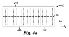
可変屈折率光抽出層は、層の横断面にわたるいくつかの所望の幾何学的配列で、互いに対して配置された第1及び第2の領域を含むことができ、結果として、層が所望の光学性能特性を提供する。図4aは、第1及び第2の領域の例示的な幾何学的配列を示す可変屈折率光抽出層の平面図である。可変屈折率光抽出層400は、層の平面図に確認されるように、層にわたって連続的な第1の領域410、及び破線を使用して示される矩形によって取り囲まれた別個の領域である第2の領域420を含む。先に記載したように、破線は、第1及び第2の領域のおよその位置を示すために、本開示の全体にわたって使用されるが、これらの破線は、領域間の何らかの種類の境界を説明するものではない。
The variable refractive index light extraction layer can include first and second regions disposed relative to one another in some desired geometric arrangement across the cross section of the layer so that the layer is as desired Provides optical performance characteristics. FIG. 4a is a plan view of the variable index light extraction layer showing an exemplary geometric arrangement of the first and second regions. The variable index
第2の領域420は、実質的に同じの長さ及び幅の矩形又はストライプとして成形され、層400の幅にわたって延在し、左から右に次第に数を増して配置される。第2の領域420は、いくつかの実施形態では少なくとも約0.03の差で、第1の領域410の屈折率よりも高い屈折率を有する。図4bは、可変屈折率光抽出層400の屈折率分布を示し、x軸は、図4aに示されるようないずれかの実質的に単一位置w1での層の長さ方向の位置dを識別する。屈折率分布は、第1及び第2の屈折率n1及びn2の間のそれぞれにパターンを含んだ、層400の屈折率の変化を示す。図4c及び図4dはそれぞれ、選択された光学的特性%透過率及び%透明度の分布を示し、両方の特性に対して、層の長さ方向で、実質的にほとんど変化が存在しない。
The
図5aは、第1及び第2の領域の例示的な幾何学的配列を示す別の可変屈折率光抽出層の平面図である。可変屈折率光抽出層500は、層の平面図に確認されるように層にわたる第1の領域510、及び破線を使用して示される円形によって取り囲まれた別個の領域である第2の領域520を含む。いくつかの実施形態では、第1及び第2の領域は、図5aとは逆にされてもよく、すなわち、第1の領域が形状により取り囲まれてもよい。パターンはまた、第2の領域520の密度がx及びy次元の両方で変化することができることを示す。
FIG. 5a is a plan view of another variable index light extraction layer showing an exemplary geometric arrangement of first and second regions. The variable index
図5bは、第1及び第2の領域の例示的な幾何学的配列を示す別の可変屈折率光抽出層の平面図である。可変屈折率光抽出層530は、層の平面図に確認されるように層にわたる第1の領域540、及び破線を使用して示されるような、形状、この場合にはハート形、によって取り囲まれた別個の領域である第2の領域550を含む。いくつかの実施形態では、第1及び第2の領域は、図5bとは逆にされてもよく、すなわち、第1の領域が形状により取り囲まれてもよい。高屈折率領域の幾何学的配列が、勾配の形で変化する必要がなく、隣接する透明な層からの超臨界光の画像対応抽出を提供するためにパターン化されてもよいことを、パターンは示す。
FIG. 5b is a plan view of another variable index light extraction layer showing an exemplary geometric arrangement of the first and second regions. The variable index
可変光抽出層の第1及び第2の領域の幾何学的配列は、隣接する透明な層内を伝播する超臨界光を抽出し、かつ可変屈折率光抽出層の対向側の別の層にパターンで、例えば実質的に均一な照明で、その光を送達するように、設計されてもよい。 The geometric arrangement of the first and second regions of the variable light extraction layer extracts supercritical light propagating in the adjacent transparent layer, and is separated into another layer opposite to the variable refractive index light extraction layer. It may be designed to deliver the light in a pattern, for example with substantially uniform illumination.
可変屈折率光抽出層は、基材上に配置されてもよい。基材としては、PCT出願米国特許出願公開第2011/021053号(Wolkら)に説明されるような層を製造するために使用される支持体を挙げることができる。いくつかの実施形態では、光学フィルムが、透明な基材上に配置された可変屈折率光抽出層を含む。本明細書で使用するとき、「透明な」は、実質的に光学的に透明で、並びに実質的に低ヘイズ及び非散乱であることを意味する。例示的な透明な基材は、光学フィルムの所望の特性に応じて、必要な光学的特性を有する。透明な基材には、ポリエステル、ポリ(メタ)アクリレート、ポリカーボネートなどの、ポリマー基材が挙げられる。いくつかの実施形態では、透明な基材は、以下に説明されるような光導体を含む。いくつかの実施形態では、光が、反射性散乱要素層650へ向かう前方向に散乱することができるように、透明な基材が、ある程度のヘイズを有し、若干の光散乱を提供することができる。
The variable refractive index light extraction layer may be disposed on the substrate. The substrate can include a support used to produce a layer as described in PCT application US 2011/021053 (Walk et al.). In some embodiments, the optical film includes a variable index light extraction layer disposed on a transparent substrate. As used herein, “transparent” means substantially optically transparent and substantially low haze and non-scattering. Exemplary transparent substrates have the necessary optical properties depending on the desired properties of the optical film. Transparent substrates include polymer substrates such as polyester, poly (meth) acrylate, polycarbonate and the like. In some embodiments, the transparent substrate comprises a light guide as described below. In some embodiments, the transparent substrate has some haze and provides some light scattering so that light can be scattered in the forward direction towards the reflective
図6は、装置によって照明される反射性散乱要素と組み合わせた可変屈折率光抽出層を含んだ、例示的な照明装置600の概略図である。照明装置600は、可変光抽出層630に隣接して配置された光導体610を含む。光導体は、可変屈折率光抽出層630の上表面625に、光学的に連結される(2つの表面の間に破線によって表示される)。単純化のために層の形態で示される反射性散乱要素650が、可変屈折率光抽出層の対向表面635に隣接する。反射性散乱要素は、可変屈折率光抽出層の下表面635に、光学的に連結される(2つの表面の間に破線によって表示される)。光源によって放射される光が光導体に入ることができるように、光源601が光導体610に光学的に連結される。いくつかの実施形態では、光学的な連結が生じるように、光導体610の下表面615と可変屈折率光抽出層630の上表面625との間にエアギャップが存在せず、かつ可変屈折率光抽出層630の下表面635と反射性散乱要素650の表面645との間にエアギャップが存在しない。
FIG. 6 is a schematic diagram of an
いくつかの実施形態では、光導体610は、可変屈折率光抽出層の第1の領域の屈折率と第2の領域の屈折率との中間の屈折率を有する。
In some embodiments, the
いくつかの実施形態では、可変光抽出層630は、反射性散乱要素650の表面645上に直接配置できる。光導体610は、いくつかの方法により、可変光抽出層の表面625に直接取り付けできる。以下に説明されるように、光導体610は、熱可塑性樹脂材料、例えばアクリルを含むことができ、これらの場合には、光導体は、可変屈折率抽出層の表面625上へ溶融樹脂をキャスティングすることによって形成できるか、又はインサート射出成形プロセスによって可変屈折率抽出層に取り付けできる。いくつかの場合には、光導体610は、可変屈折率抽出層の表面625に熱積層できるように、エラストマー材料を含む。いくつかの場合には、光導体610は、可変屈折率抽出層の表面625に直接積層できるように、感圧接着剤(PSA)を含む。光導体610が接着剤ではない場合には、可変屈折率光抽出層の表面625は、光学的に透明な接着剤を使用して光導体の表面615に接着することができる。光学的に透明な接着剤は、以下に説明される。
In some embodiments, the variable
光導体610は、任意の好適な材料(単数又は複数)を含むことができる。例えば、光導体としては、ガラス、ポリメチルメタクリレートを含むアクリレート、ポリカーボネート、ポリスチレン、スチレンメタクリレートコポリマー及びブレンド、シクロオレフィンポリマー(例えば、ケンタッキー州ルイビルのZEON Chemicals L.P.から入手可能なZEONEX及びZEONOR)、フルオロポリマー、ポリエステル(ポリエチレンテレフタレート(PET)、ポリエチレンナフタレート(PEN)、及びPET若しくはPEN又はその両方を含有するコポリマー)、ポリウレタン、エポキシ、ポリオレフィン(ポリエチレン、ポリプロピレン、ポリノルボルネン、アイソタクチック、アタクチック、及びシンジオタクチック立体異性体のポリオレフィン、並びにメタロセン重合によって生成されるポリオレフィン)を挙げることができる。いくつかの場合には、光導体は、エラストマー性ポリウレタン材料、並びにポリジアルキルシロキサン、シリコーンポリ尿素、及びシリコーンポリオキサミドを含むがこれらに限定されないシリコーン系ポリマーなどの、エラストマーであることができる。
The
いくつかの実施形態では、光導体は、国際公開第2010/005655(A2)号(Shermanら)において説明されるような、粘弾性光導体である。一般に、粘弾性光導体は、変形するときに弾性及び粘性挙動の両方を示す1つ又は複数の粘弾性材料を含む。弾性特性は、過渡的荷重が除去された後に元の形状に戻る材料の能力を指す。材料に対する弾性の1つの尺度は、材料がその長さの2倍に引き伸ばされ、続いて、引き伸ばされたときと同じ条件下に元に戻された(脱引き伸ばしさせた)後に残存する伸びに応じた、永久伸び値(tensile set value)と呼ばれる。材料が0%の永久伸び値を有する場合には、材料は弛緩の際に元の長さに戻り、永久伸び値が100%の場合には、弛緩の際に材料は元の長さの2倍になる。永久伸び値は、ASTM D412を使用して測定できる。有用な粘弾性材料は、約10%より大きい、約30%より大きい、若しくは約50%より大きい;又は約5〜約70%、約10〜約70%、約30〜約70%、若しくは約10〜約60%の永久伸び値を有することができる。 In some embodiments, the light guide is a viscoelastic light guide, as described in WO 2010/005655 (A2) (Sherman et al.). In general, viscoelastic lightguides include one or more viscoelastic materials that exhibit both elastic and viscous behavior when deformed. Elastic properties refer to the ability of a material to return to its original shape after a transient load is removed. One measure of elasticity for a material is a function of the elongation that remains after the material is stretched to twice its length and subsequently restored (destretched) under the same conditions as when stretched. It is also called the “tensile set value”. If the material has a permanent elongation value of 0%, the material will return to its original length upon relaxation, and if the permanent elongation value is 100%, the material will have an original length of 2 upon relaxation. Double. Permanent elongation values can be measured using ASTM D412. Useful viscoelastic materials are greater than about 10%, greater than about 30%, or greater than about 50%; or about 5 to about 70%, about 10 to about 70%, about 30 to about 70%, or about It can have a permanent elongation value of 10 to about 60%.
ニュートン流体である粘性材料は、応力が剪断勾配と共に直線的に増加することを述べたニュートンの法則に従う粘度特性を有する。剪断勾配が除去された際に、液体は形状を元に戻さない。有用な粘弾性材料の粘度特性としては、材料が分解しないような妥当な温度下での材料の流動性が挙げられる。 Viscous materials that are Newtonian fluids have viscosity properties that follow Newton's law, which states that stress increases linearly with shear gradient. When the shear gradient is removed, the liquid does not return to its original shape. Useful viscoelastic material viscosity characteristics include fluidity of the material at reasonable temperatures such that the material does not decompose.
粘弾性光導体は、粘弾性光導体及び光学物品が光学的に連結されるように、光導体からの光を抽出するべく設計された材料の少なくとも一部分、例えば光学物品、との十分な接触又は湿潤を容易にする特性を有することができる。次いで、光が粘弾性光導体から抽出できる。粘弾性光導体は、一般に、軟質、柔軟かつ可撓性である。したがって、粘弾性光導体は、十分な接触が得られるような弾性率(又は貯蔵弾性率G’)を、層が不必要に流れないような粘性係数(又は損失率G”)を、及び層の減衰の相対程度に対する減衰係数(G”/G’、tan D)を有することができる。有用な粘弾性材料は、0.1Gy/秒(10rad/秒)及び約20〜約22℃の温度で測定された、約300,000Pa未満の貯蔵弾性率G’を有することができる。材料の粘弾性特性は、例えば、ASTM D4065、D4440、及びD5279に従って、動的機械分析を使用して測定できる。 A viscoelastic lightguide is sufficient contact with at least a portion of a material designed to extract light from the lightguide, such as an optical article, such that the viscoelastic lightguide and the optical article are optically coupled. It can have properties that facilitate wetting. Light can then be extracted from the viscoelastic light guide. Viscoelastic light guides are generally soft, soft and flexible. Thus, the viscoelastic light guide has an elastic modulus (or storage elastic modulus G ′) that provides sufficient contact, a viscosity coefficient (or loss rate G ″) that prevents the layer from flowing unnecessarily, and a layer. Can have an attenuation coefficient (G ″ / G ′, tan D) for the relative degree of attenuation. Useful viscoelastic materials may have a storage modulus G 'of less than about 300,000 Pa measured at a temperature of 0.1 Gy / sec (10 rad / sec) and from about 20 to about 22 ° C. The viscoelastic properties of the material can be measured using dynamic mechanical analysis, for example, according to ASTM D4065, D4440, and D5279.
いくつかの実施形態では、粘弾性光導体は、ダルキスト基準線で説明されるような(Handbook of Pressure Sensitive Adhesive Technology,Second Ed.,D.Satas編、Van Nostrand Reinhold,ニューヨーク,1989年に説明されるような)、PSA層を含む。 In some embodiments, the viscoelastic lightguide is as described in the Dalquist baseline (Handbook of Pressure Sensitive Technology, Second Ed., Ed. D. Satas, Ed., Van Nostrand Reinhold, 198). Including a PSA layer.
粘弾性光導体は、特定の剥離力を有するか、又は少なくとも、特定の範囲内の剥離力を示すことができる。例えば、粘弾性光導体は、約50〜約3000g/in(0.02〜約1N/mm)、約300〜約3000g/in(0.1〜約1N/mm)、又は約500〜約3000g/in(0.2〜約1N/mm)の90度剥離力を有することができる。剥離力は、マサチューセッツ州マーシュフィールドのIMASSから入手可能な剥離試験機を使用して測定できる。 The viscoelastic light guide may have a specific peel force or at least exhibit a peel force within a specific range. For example, the viscoelastic light guide may be about 50 to about 3000 g / in (0.02 to about 1 N / mm), about 300 to about 3000 g / in (0.1 to about 1 N / mm), or about 500 to about 3000 g. 90 degree peel force of / in (0.2 to about 1 N / mm). Peel force can be measured using a peel tester available from IMASS, Marshfield, Massachusetts.
いくつかの実施形態では、粘弾性光導体は、可視光スペクトル(約400〜約700nm)の少なくとも一部分にわたって約80〜約100%、約90〜約100%、約95〜約100%、又は約98〜約100%の高い光透過率を有した光学的に透明な光導体を含む。いくつかの実施形態では、粘弾性光導体は、約5%未満、約3%未満、又は約1%未満のヘイズ値を有する。いくつかの実施形態では、粘弾性光導体は、約0.01%から約5%未満、約0.01%から約3%未満、又は約0.01%から約1%未満のヘイズ値を有する。透過状態におけるヘイズ値は、ASTM D1003に従ってヘイズメーターを使用して測定できる。 In some embodiments, the viscoelastic lightguide is about 80 to about 100%, about 90 to about 100%, about 95 to about 100%, or about about at least a portion of the visible light spectrum (about 400 to about 700 nm). It includes an optically transparent light guide having a high light transmission of 98 to about 100%. In some embodiments, the viscoelastic lightguide has a haze value of less than about 5%, less than about 3%, or less than about 1%. In some embodiments, the viscoelastic lightguide has a haze value of about 0.01% to less than about 5%, about 0.01% to less than about 3%, or about 0.01% to less than about 1%. Have. The haze value in the transmissive state can be measured using a haze meter according to ASTM D1003.
いくつかの実施形態では、粘弾性光導体は、高い光透過率及び低いヘイズ値を有した光学的に透明な光導体を含む。高い光透過率は、可視光スペクトル(約400〜約700nm)の少なくとも一部分にわたって、約90〜約100%、約95〜約100%、又は約99〜約100%であってもよく、ヘイズ値は、約0.01%から約5%未満、約0.01%から約3%未満、又は約0.01%から約1%未満であってもよい。粘弾性光導体はまた、約50〜約100%の光透過率を有してもよい。 In some embodiments, the viscoelastic lightguide comprises an optically clear lightguide having a high light transmission and a low haze value. The high light transmittance may be about 90 to about 100%, about 95 to about 100%, or about 99 to about 100% over at least a portion of the visible light spectrum (about 400 to about 700 nm), and has a haze value May be from about 0.01% to less than about 5%, from about 0.01% to less than about 3%, or from about 0.01% to less than about 1%. The viscoelastic light guide may also have a light transmission of about 50 to about 100%.
粘弾性光導体は、約1.3〜約2.6、1.4〜約1.7、又は約1.5〜約1.7の範囲の屈折率を有してもよい。粘弾性光導体のために選択される特定の屈折率又は屈折率の範囲は、照明装置の設計全体、及び装置が使用できる特定の用途に依存してよい。 The viscoelastic lightguide may have a refractive index in the range of about 1.3 to about 2.6, 1.4 to about 1.7, or about 1.5 to about 1.7. The particular refractive index or range of refractive indices selected for the viscoelastic light guide may depend on the overall design of the lighting device and the particular application that the device can use.
粘弾性光導体材料は、粘弾性光導体材料の屈折率を修正することができ又は粘弾性光導体材料の機械的特性に影響を及ぼすナノ粒子を含んでもよい。好適なナノ粒子は、粒子がかなり量の散乱を光導体材料に導入せずに所望の効果をもたらすような、サイズを有する。 The viscoelastic lightguide material may include nanoparticles that can modify the refractive index of the viscoelastic lightguide material or affect the mechanical properties of the viscoelastic lightguide material. Suitable nanoparticles have a size such that the particles provide the desired effect without introducing a significant amount of scattering into the light guide material.
粘弾性光導体は、少なくとも1つのポリマーを一般的に含む。粘弾性光導体は、少なくとも1つの感圧接着剤(PSA)を含んでもよい。PSAは、被着体を緊密に接着するために有用であり、(1)強力かつ恒久的な粘着性、(2)指圧以下での接着、(3)被着体上に留まるのに十分な能力、(4)被着体からきれいに除去可能な十分な凝集強度、などの特性を示す。感圧接着剤としてうまく機能することが見出された材料は、粘着性、引き剥がし粘着力、及び剪断保持力の所望のバランスをもたらす必要な粘弾性特性を示すように設計及び配合されたポリマーである。 Viscoelastic light guides typically comprise at least one polymer. The viscoelastic light guide may comprise at least one pressure sensitive adhesive (PSA). PSA is useful for intimately adhering adherends, (1) strong and permanent tack, (2) adhesion under finger pressure, (3) sufficient to remain on the adherend Properties such as ability and (4) sufficient cohesive strength that can be removed cleanly from the adherend. Materials that have been found to function well as pressure sensitive adhesives are polymers designed and formulated to exhibit the necessary viscoelastic properties that provide the desired balance of tack, peel adhesion, and shear retention It is.
有用なPSAは、先に引用されたShermanらの参照文献に詳細に説明される。有用なPSAとしては、モノマーのホモポリマーが約0度以下のTgを有する、少なくとも1つのモノエチレン性不飽和アルキル(メタ)アクリレートモノマーを含むモノマーAと、モノマーのホモポリマーがモノマーAのTgよりも高いTg、例えば少なくとも約10℃を有する、少なくとも1つのモノエチレン性不飽和フリーラジカル共重合性強化モノマーを含むモノマーBと、から誘導されるポリ(メタ)アクリレートPSAが挙げられる。本明細書で使用するとき、(メタ)アクリルは、アクリル種及びメタクリル種の両方を指し、(メタ)アクリレートに対してもまた同様である。 Useful PSAs are described in detail in the Sherman et al reference cited above. Useful PSAs include monomer A comprising at least one monoethylenically unsaturated alkyl (meth) acrylate monomer, wherein the monomer homopolymer has a Tg of about 0 degrees or less, and the monomer homopolymer is greater than the Tg of monomer A And poly (meth) acrylate PSA derived from monomer B containing at least one monoethylenically unsaturated free radical copolymerizable reinforcing monomer having a higher Tg, for example at least about 10 ° C. As used herein, (meth) acryl refers to both acrylic and methacrylic species, as well as to (meth) acrylates.
いくつかの実施形態では、粘弾性光導体は、天然ゴム系及び合成ゴム系PSA、熱可塑性エラストマー、粘着付与された熱可塑性エポキシ誘導体、ポリウレタン誘導体、ポリウレタンアクリレート誘導体、シリコーンPSA(ポリジオルガノシロキサン、ポリジオルガノシロキサンポリオキサミド、及びシリコーン尿素ブロックコポリマーなど)を含む。 In some embodiments, the viscoelastic lightguide comprises a natural rubber and synthetic rubber PSA, a thermoplastic elastomer, a tackified thermoplastic epoxy derivative, a polyurethane derivative, a polyurethane acrylate derivative, a silicone PSA (polydiorganosiloxane, polydioxysiloxane). Organosiloxane polyoxamide, and silicone urea block copolymer).
いくつかの実施形態では、粘弾性光導体は、例えば、3M社のVHB(商標)Acrylic Tape 4910F又は4918、並びに3M(商標)Optically Clear Laminating Adhesives(8140及び8180シリーズ)といった転写テープとして入手可能な透明アクリルPSAなどの、透明アクリルPSAを含む。 In some embodiments, the viscoelastic light guide is available as a transfer tape, such as 3M VHB ™ Acrylic Tape 4910F or 4918, and 3M ™ Optically Clear Laminating Adhesives (8140 and 8180 series). Includes transparent acrylic PSA, such as transparent acrylic PSA.
いくつかの実施形態では、粘弾性光導体は、ルイス酸−塩基対を形成するために接着剤マトリックス内に分散するブロックコポリマーを含む。いくつかの実施形態では、粘弾性光導体は、0度の角度で又はほぼ0度の角度で引き伸ばされるときに基材から除去できる、伸長剥離可能なPSAを含む。 In some embodiments, the viscoelastic lightguide comprises a block copolymer that is dispersed within the adhesive matrix to form a Lewis acid-base pair. In some embodiments, the viscoelastic lightguide comprises a stretch peelable PSA that can be removed from the substrate when stretched at an angle of 0 degrees or at an angle of approximately 0 degrees.
いくつかの実施形態では、光導体610は、外表面605上に、追加的なコーティング、又はコーティングを有した上層フィルムを含むことができる。追加のコーティング又はフィルムは、光導体の表面に対する任意の所望の特性のために設計できる。コーティングの例としては、例えば、ハードコート、反射防止コーティング、防汚コーティング、ツヤ消しコーティング、防曇コーティング、耐引っかきコーティング、プライバシーコーティング、又はこれらの組み合わせが挙げられる。強化された耐久性を提供するハードコート、防曇コーティング、及び耐引っかきコーティングのようなコーティングは、例えば、タッチスクリーンセンサ、ディスプレイスクリーン、グラフィック用途などの、用途において望ましい。プライバシーコーティングの例としては、例えば、ぼんやりとした視界をもたらすための不鮮明若しくは霞んだコーティング、又は視角を制限するためのルーバー付フィルムが挙げられる。コーティングがフィルムとして提供されるいくつかの場合には、光導体の屈折率よりも低い屈折率を有した接着剤でフィルムを光導体610の表面605に接着することが望ましい。代替的に、ナノボイド化層が、光導体610の上表面605と追加的な上層フィルムの下部との間に配置されてもよい。
In some embodiments, the
先に記載したように、光導体610は、光学的に透明な接着剤(OCA)を使用して、可変屈折率光抽出層630に接着できる。いくつかの実施形態では、OCAは、可視光スペクトル(約400〜約700nm)の少なくとも一部分にわたって約80〜約100%、約90〜約100%、約95〜約100%、若しくは約98〜約100%の高い光透過率、及び/又は約0.01%から約5%未満、約0.01%から約3%未満、若しくは約0.01%から約1%未満のヘイズ値を有したPSAを含む。
As described above, the
いくつかの実施形態では、有用なPSAは、ダルキスト基準線で説明されるような(Handbook of Pressure Sensitive Adhesive Technology,Second Ed.,D.Satas編、Van Nostrand Reinhold,ニューヨーク,1989年に説明されるような)、PSAを含む。PSAは、特定の剥離力を有するか、又は少なくとも、特定の範囲内の剥離力を示してもよい。例えば、PSAは、約10〜約3000g/in(0.004〜約1N/mm)、約300〜約3000g/in(0.1〜約1N/mm)、又は約500〜約3000g/in(0.2〜約1N/mm)の90度剥離力を有することができる。剥離力は、マサチューセッツ州マーシュフィールドのIMASSから入手可能な剥離試験機を使用して測定できる。 In some embodiments, useful PSA's are described in the Dalquist baseline (Handbook of Pressure Sensitive Technology, Second Ed., Edited by D. Satas, Van Nostrand Reinhold, 198). PSA). The PSA may have a specific peel force or at least exhibit a peel force within a specific range. For example, the PSA can be about 10 to about 3000 g / in (0.004 to about 1 N / mm), about 300 to about 3000 g / in (0.1 to about 1 N / mm), or about 500 to about 3000 g / in ( 90 degree peel force of 0.2 to about 1 N / mm). Peel force can be measured using a peel tester available from IMASS, Marshfield, Massachusetts.
OCAは、約1.3〜約2.6、1.4〜約1.7、又は約1.5〜約1.7の範囲の屈折率を有してもよい。OCAのために選択される特定の屈折率又は屈折率の範囲は、光導体及び可変屈折率光抽出層を含む光学フィルムの設計全体に左右される。一般に、OCAは、光導体の屈折率とおよそ等しいか又は光導体の屈折率よりも高く、可変屈折率光抽出層630の第1の領域の屈折率と第2の領域の屈折率との間の、屈折率を有しなければならない。
The OCA may have a refractive index in the range of about 1.3 to about 2.6, 1.4 to about 1.7, or about 1.5 to about 1.7. The particular index or range of indices selected for OCA depends on the overall design of the optical film including the light guide and the variable index light extraction layer. In general, OCA is approximately equal to or higher than the refractive index of the light guide, and is between the refractive index of the first region and the second region of the variable refractive index
OCAとして使用されるPSAは、粘弾性光導体のために先に説明された材料のうちのいずれかを含んでもよい。PSAである追加の例示的なOCAは、米国特許第7,005,394号(Ylitaloら)に説明されるような粘着付与された熱可塑性エポキシ、同3,718,712号(Tushaus)に説明されるようなポリウレタン、米国特許出願第2006/0216523号(Shusuke)に説明されるようなポリウレタンアクリレートを含む。いくつかの実施形態では、接着剤は、例えば、3M社のVHB(商標)Acrylic Tape 4910F及び4918、3M(商標)Optically Clear Laminating Adhesives(8140及び8180シリーズ)、並びに国際公開第2004/0202879号に説明される3M(商標)Optically Clear Laminating Adhesives(8171CL及び8172CL)といった転写テープとして入手可能な透明アクリルPSAなどの、透明アクリルPSAを含む。有用なOCAはまた、米国特許出願第2011/0039099号(Shermanら)に説明される。いくつかの実施形態では、OCAは、例えば米国特許出願第2007/0212535号(Shermanら)に説明されるような、光導体の表面への適用の際に空気放出を可能にするためにマイクロ構造体化接着表面を有したPSAを含むことができる。 The PSA used as the OCA may include any of the materials previously described for the viscoelastic light guide. An additional exemplary OCA that is a PSA is described in a tackified thermoplastic epoxy as described in US Pat. No. 7,005,394 (Ylitalo et al.), US Pat. No. 3,718,712 (Tushaus). Polyurethanes such as those described in US Patent Application Publication No. 2006/0216523 (Shusuke). In some embodiments, the adhesive is, for example, from 3M VHB (TM) Acrylic Tape 4910F and 4918, 3M (TM) Optically Clear Laminating Adhesives (8140 and 8180 series), and International Publication No. 2004/0202879. Transparent acrylic PSA, such as transparent acrylic PSA available as a transfer tape, such as the 3M ™ Optically Clear Laminating Adhesives (8171CL and 8172CL) described. Useful OCAs are also described in US Patent Application No. 2011/0039099 (Sherman et al.). In some embodiments, the OCA is microstructured to allow air release upon application to the surface of the light guide, as described, for example, in US Patent Application No. 2007/0212535 (Sherman et al.). A PSA having an integrated adhesive surface can be included.
接着剤は、伸長剥離可能なPSAを含んでもよい。伸長剥離可能なPSAは、0度の角度で又はほぼ0度の角度で引き伸ばされる場合に基材から除去できるPSAである。いくつかの実施形態では、接着剤、又は光学テープとして使用される伸長剥離可能なPSAは、1rad/秒(0.01Gy/秒)及び−17℃で測定されるとき、約10MPa未満、1rad/秒(0.01Gy/秒)及び−17℃で測定されるとき、約0.03〜約10MPaの剪断貯蔵弾性率を有する。伸長剥離可能なPSAは、分解、再加工、又はリサイクルが望ましい場合に、使用できる。 The adhesive may include a stretchable peelable PSA. Stretchable PSA is PSA that can be removed from a substrate when stretched at an angle of 0 degrees or at an angle of approximately 0 degrees. In some embodiments, the stretch-releasable PSA used as an adhesive or optical tape is less than about 10 MPa, 1 rad / second (0.01 Gy / second) and -17 ° C. when measured at −17 ° C. It has a shear storage modulus of about 0.03 to about 10 MPa when measured at seconds (0.01 Gy / sec) and −17 ° C. Stretchable PSA can be used where disassembly, rework, or recycling is desired.
いくつかの実施形態では、伸長剥離可能なPSAは、米国特許第6,569,521(B1)号(Sheridanら)又は米国特許仮出願第61/020423号(63934US002、Shermanら)及び同第61/036501号(64151US002、Determanら)に説明されるようなシリコーン系PSAを含むことができる。このようなシリコーン系PSAは、MQ粘着付与樹脂及びシリコーンポリマーの組成物を含む。例えば、伸長剥離可能なPSAは、MQ粘着付与樹脂、並びに尿素系シリコーンコポリマー、オキサミド系シリコーンコポリマー、アミド系シリコーンコポリマー、ウレタン系シリコーンコポリマー、及びこれらの混合物を含む群から選択されるエラストマーシリコーンポリマーを含むことができる。 In some embodiments, the stretch-peelable PSA is US Pat. No. 6,569,521 (B1) (Sheridan et al.) Or US Provisional Application No. 61/020423 (63934 US002, Sherman et al.) / 036501 (64151 US002, Determan et al.) Can include silicone-based PSA. Such silicone-based PSA includes a composition of MQ tackifying resin and silicone polymer. For example, the stretch peelable PSA comprises an MQ tackifying resin and an elastomeric silicone polymer selected from the group comprising urea-based silicone copolymers, oxamide-based silicone copolymers, amide-based silicone copolymers, urethane-based silicone copolymers, and mixtures thereof. Can be included.
いくつかの実施形態では、伸長剥離可能なPSAは、国際公開第2010/078346号(Yamanakaら)及び同2010/077541号(Tranら)に説明されるようなアクリレート系PSAを含むことができる。このようなアクリレート系のPSAは、アクリレート、無機粒子、及び架橋剤の組成物を含む。これらのPSAは、単層又は多層であることができる。 In some embodiments, the stretch peelable PSA can comprise an acrylate-based PSA as described in WO 2010/078346 (Yamanaka et al.) And 2010/077751 (Tran et al.). Such acrylate-based PSA includes a composition of acrylate, inorganic particles, and a crosslinker. These PSAs can be single layer or multilayer.
いくつかの実施形態では、接着層は、米国特許第7,862,898号(Shermanら)及び同第7,892,649号(Shermanら)に説明されるような多官能性エチレン性不飽和シロキサンポリマ−及び1つ又は複数のビニルモノマーの硬化反応生成物を含むことができる。 In some embodiments, the adhesive layer is a polyfunctional ethylenically unsaturated as described in US Pat. Nos. 7,862,898 (Sherman et al.) And 7,892,649 (Sherman et al.). A curing reaction product of a siloxane polymer and one or more vinyl monomers can be included.
いくつかの実施形態では、国際公開第2010/132176号(Shermanら)及び同2009/085662号(Shermanら)に説明されるような自己湿潤型接着剤の使用が、反射性散乱要素上への照明装置600の定置において有益である。
In some embodiments, the use of a self-wetting adhesive as described in WO 2010/132176 (Sherman et al.) And 2009/088562 (Sherman et al.) Can be used on reflective reflective elements. This is useful in the placement of the
例示的なPSAは、ポリエーテルセグメントを含むオリゴマー及び/又はモノマーから誘導されるポリマーを含み、そのポリマーの35〜85重量%が、ポリエーテルセグメントを含む。これらの接着剤は、米国特許出願第2007/0082969A1号(Malikら)に説明される。別の例示的なPSAは、フリーラジカル重合性ウレタン系又は尿素系オリゴマー及びフリーラジカル重合性セグメント化シロキサン系コポリマーの反応生成物を含み、これらの接着剤は、米国特許仮出願第61/410510号(Tapioら、代理人整理番号第67015US002号)に説明される。 Exemplary PSAs include polymers derived from oligomers and / or monomers containing polyether segments, and 35-85% by weight of the polymer contains polyether segments. These adhesives are described in US Patent Application No. 2007 / 0082969A1 (Malik et al.). Another exemplary PSA includes the reaction product of a free-radically polymerizable urethane-based or urea-based oligomer and a free-radically polymerizable segmented siloxane-based copolymer, and these adhesives are described in US Provisional Application No. 61/410510. (Tapio et al., Agent reference number 67015 US002).
PSAは、ナノ粒子、可塑剤、連鎖移動剤、開始剤、抗酸化剤、安定剤、粘度調整剤、及び帯電防止剤などの、1つ又は複数の添加剤を任意に含むことができる。 The PSA can optionally include one or more additives such as nanoparticles, plasticizers, chain transfer agents, initiators, antioxidants, stabilizers, viscosity modifiers, and antistatic agents.
いくつかの実施形態では、シール層が、可変屈折率光抽出層をもたらすために、パターン化されたナノボイド化低屈折率層を覆って配置される。シール層は、ナノボイド化層内への汚染物質の浸透を最小化するために使用できる。例えば、シール層がパターン化された屈折率領域を含む領域(図1cの可変屈折率領域100)と接着層との間にあるように、シール層が、パターン化された低屈折率領域を覆って低屈折率領域の間に配置されることができ、したがって、可変屈折率光抽出層を形成する。別の例としては、シール層が、パターン化された屈折率領域と光導体との間にあるように、可変屈折率光抽出層を形成するパターン化された低屈折率層を覆って配置されことができ、シール層が、光導体の屈折率とおよそ等しいか又は光導体の屈折率よりも高い屈折率を有する。
In some embodiments, a seal layer is disposed over the patterned nanovoided low index layer to provide a variable index light extraction layer. The seal layer can be used to minimize the penetration of contaminants into the nanovoided layer. For example, the seal layer covers the patterned low index region so that the seal layer is between the region including the patterned index region (
好適なシール層は感圧接着剤ポリマー及びコポリマーを含み、感圧接着剤ポリマー及びコポリマーは、アクリル又はアクリレート系、スチレンブタジエン、又はスチレンイソプレン型コポリマー熱可塑性樹脂、及びナノボイド化された第1の領域内への浸透が可能な低分子量種を有意な画分で含有していない場合の類似のポリマー、であることができる。他のポリマーシール層は、アクリル、アクリル−酢酸ビニル、コポリマー、ブロックコポリマー、EVAコポリマー、ポリアミド、ポリエステル、ポリエチレンポリマー及びコポリマー、ポリイソブチレン、ポリプロピレンポリマー及びコポリマー、ポリウレタンポリマー及びコポリマー、並びにサーリンプラスチック、酢酸ビニル、及びポリフッ化ビニリデンポリマーを含む他のポリマー、それらのアロイ、コポリマー、及び酸塩類を有する誘導体、を含む熱活性化接着剤ポリマーであることができる。これらの材料は、メルトコーティングによって塗布されるか、又は任意の好適なコーティング方法によってポリマーの水性又は溶媒系エマルジョン又は分散液からコーティングされ、直接フィルム積層によって積層されるか。シール層として有用な、好適なポリマー分散液の2つの例は、(オランダヘールレンのDSMから入手可能な)NEOCRYL A−614及びNEOPAC R−9699である。シール層はまた、樹脂成分がナノ多孔質低屈折率領域のナノボイドに浸透しないようにオーバーコーティング及び硬化できる硬化性樹脂系を含んでもよい。 Suitable seal layers include pressure sensitive adhesive polymers and copolymers, the pressure sensitive adhesive polymers and copolymers being acrylic or acrylate based, styrene butadiene, or styrene isoprene type copolymer thermoplastics, and a nanovoided first region. It can be a similar polymer if it does not contain a significant fraction of low molecular weight species that can penetrate into it. Other polymer sealing layers include acrylic, acrylic-vinyl acetate, copolymers, block copolymers, EVA copolymers, polyamides, polyesters, polyethylene polymers and copolymers, polyisobutylene, polypropylene polymers and copolymers, polyurethane polymers and copolymers, and Surlyn plastics, vinyl acetate And other polymers including polyvinylidene fluoride polymers, their alloys, copolymers, and derivatives with acid salts, can be heat-activated adhesive polymers. Are these materials applied by melt coating or are coated from an aqueous or solvent-based emulsion or dispersion of polymer by any suitable coating method and laminated directly by film lamination? Two examples of suitable polymer dispersions useful as seal layers are NEOCRYL A-614 and NEOPAC R-9699 (available from DSM, Heerlen, The Netherlands). The sealing layer may also include a curable resin system that can be overcoated and cured so that the resin component does not penetrate the nanovoids in the nanoporous low refractive index region.
光源は、光源からの光の少なくとも一部が光導体に入ることができるように、光導体に光学的に連結される。例えば、光源は、光源によって放射される光のうちの1%超、10%超、20%超、30%超、40%超、50%超、90%超、又は約100%が光導体に入るように、光導体に光学的に連結することができる。別の例としては、光源は、光源によって放射される光のうちの約1%〜約10%、約1%〜約20%、約1%〜約30%、約1%〜約40%、約1%〜約50%、約1%〜約100%、約1%〜約100%、約50%〜約100%、又は約1%〜約100%が光導体に入るように、光導体に光学的に連結できる。光源は、ランダムな又は特定の角度分布を有する光を放射することができる。 The light source is optically coupled to the light guide so that at least a portion of the light from the light source can enter the light guide. For example, the light source may have more than 1%, more than 10%, more than 20%, more than 30%, more than 40%, more than 50%, more than 90%, or about 100% of the light emitted by the light source in the light guide. It can be optically coupled to the light guide to enter. As another example, the light source is about 1% to about 10%, about 1% to about 20%, about 1% to about 30%, about 1% to about 40% of the light emitted by the light source, The light guide such that about 1% to about 50%, about 1% to about 100%, about 1% to about 100%, about 50% to about 100%, or about 1% to about 100% enter the light guide. Can be optically coupled to. The light source can emit light having a random or specific angular distribution.
光源は任意の好適な光源を含むことができる。例示的な光源としては、冷陰極蛍光ランプなどの線状光源、及び発光ダイオード(LED)などの点光源が挙げられる。例示的な光源としてはまた、有機発光デバイス(OLED)、白熱電球、蛍光灯、ハロゲンランプ、UV電球、赤外線源、近赤外線源、レーザ、又は化学光源が挙げられる。一般に、光源によって放射される光は、可視であっても又は不可視であってもよい。少なくとも1つの光源が使用できる。例えば、1〜約10,000個の光源が使用できる。光源は、光導体の縁又は縁の近傍に位置付けられたLEDの列を含んでもよい。光源は、LEDから放射された光が光導体を所望の区域全体にわたり連続的又は均一に照らすように回路上に配置されたLEDを含んでもよい。光源は、色が光導体内で混じり合うことができるように、異なる色の光を放射するLEDを含んでもよい。 The light source can include any suitable light source. Exemplary light sources include linear light sources such as cold cathode fluorescent lamps and point light sources such as light emitting diodes (LEDs). Exemplary light sources also include organic light emitting devices (OLEDs), incandescent bulbs, fluorescent lamps, halogen lamps, UV bulbs, infrared sources, near infrared sources, lasers, or chemical light sources. In general, the light emitted by the light source may be visible or invisible. At least one light source can be used. For example, from 1 to about 10,000 light sources can be used. The light source may include an array of LEDs positioned at or near the edge of the light guide. The light source may include an LED disposed on the circuit such that light emitted from the LED illuminates the light guide continuously or uniformly over the desired area. The light source may include LEDs that emit different colors of light so that the colors can mix within the light guide.
「LED」は、可視、紫外、又は赤外であるかどうかを問わず、光を放射するダイオードを指す。これには、従来のもの又は超高輝度のものであるかによらず、「LED」として市販されているインコヒーレントな封入又はカプセル化された半導体デバイスを含む。LEDが紫外線などの非可視光線を発する場合、及びLEDが可視光線を発するある特定の場合、LEDは蛍光体を含むようにパッケージ化され(あるいは遠隔配置された蛍光体を照射することができ)、短波長の光を長波長の可視光線に変え、特定の場合には白色光を発する装置を提供する。 “LED” refers to a diode that emits light, whether visible, ultraviolet, or infrared. This includes incoherent encapsulated or encapsulated semiconductor devices marketed as “LEDs”, whether conventional or ultra-bright. If the LED emits invisible light, such as ultraviolet light, and in certain cases where the LED emits visible light, the LED is packaged to contain a phosphor (or can illuminate a remotely located phosphor) Provide a device that converts short wavelength light into long wavelength visible light and emits white light in certain cases.
「LEDダイ」は、最も基本的な形態、すなわち半導体加工手順によって作製された個々の構成要素又はチップの形態のLEDである。構成要素又はチップは、デバイスに電圧を加えるための電力の適用に適した電気接点を含むことができる。構成要素又はチップの個々の層及びその他の機能的要素は、通常、ウェハスケールで形成された後、仕上がったウェハは個々の小片部に切られて、多数のLEDダイとなることができる。 An “LED die” is an LED in its most basic form, that is, in the form of individual components or chips made by a semiconductor processing procedure. The component or chip can include electrical contacts suitable for application of power to apply a voltage to the device. After individual layers of components or chips and other functional elements are typically formed on a wafer scale, the finished wafer can be cut into individual pieces to form multiple LED dies.
白色光の生成に用いられるかどうかに関わらず、多色光源はライトアセンブリにおいて様々な形態であってよく、光導体の出光エリア、つまり出光面の色及び光度の均一性に様々な影響を及ぼす。ある手法では、複数のLEDダイ(例えば、赤色、緑色、及び青色を発光するダイ)がリード線フレーム又はその他の基板に全て互いに隣接して実装され、1つのパッケージを形成するように単一の封入体材料で一緒に封入され、この場合、パッケージにはレンズ要素が1つだけ含まれていてもよい。このような光源は、いずれか1つの個別の色、又は同時にすべての色を発光するように制御可能である。別の手法では、1パッケージにつき1つのLEDダイと1色の発光色を提供する、個別にパッケージ化されたLEDを、所定のリサイクリングキャビティに一緒にまとめて配置してよく、この集合体には青/黄、赤/緑/青、赤/緑/青/白、又は赤/緑/青/シアン/黄などの異なる色を発光するパッケージ化LEDの組み合わせが含まれる。また、琥珀色LEDも用いてよい。また別の手法では、このような個別にパッケージ化された多色LEDを1つ又は複数の線、アレイ、又はその他のパターン内で位置決めされてもよい。 Regardless of whether it is used to generate white light, multicolor light sources may take a variety of forms in the light assembly and have different effects on the light exit area of the light guide, i.e., the color and intensity uniformity of the light exit surface. . In one approach, multiple LED dies (eg, red, green, and blue light emitting dies) are all mounted adjacent to each other on a lead frame or other substrate to form a single package. Encapsulated together with an encapsulant material, in which case the package may contain only one lens element. Such a light source can be controlled to emit any one individual color or all colors simultaneously. In another approach, individually packaged LEDs that provide one LED die and one emission color per package may be placed together in a predetermined recycling cavity, and the assembly Includes combinations of packaged LEDs that emit different colors such as blue / yellow, red / green / blue, red / green / blue / white, or red / green / blue / cyan / yellow. An amber LED may also be used. In another approach, such individually packaged multicolor LEDs may be positioned in one or more lines, arrays, or other patterns.
望ましい場合には、開示するバックライトに対する照明光源として、個別のLED光源の代わりに、又はLED光源に追加して、線状の冷陰極蛍光ランプ(CCFL)又は熱陰極蛍光ランプ(HCFL)などの別の可視光線発光体を使用してもよい。更に、例えば冷白色及び温白色を含む(CCFL/LED)、CCFL/HCFL、例えば異なるスペクトルを放射するものなどのハイブリッドシステムを使用することができる。発光体の組み合わせは、幅広く異なってもよく、LEDとCCFL、及び例えば多重CCFL、異なる色の多重CCFL、及びLEDとCCFLなどの多数を含むことが可能である。また光源には、レーザ、半導体レーザ、プラズマ光源、又は有機発光ダイオードが、単体又は他の種類の光源、例えばLEDとの組み合わせで含まれてよい。 If desired, such as a linear cold cathode fluorescent lamp (CCFL) or hot cathode fluorescent lamp (HCFL) as an illumination light source for the disclosed backlight, instead of or in addition to a separate LED light source Another visible light emitter may be used. In addition, hybrid systems can be used, including, for example, cold white and warm white (CCFL / LED), CCFL / HCFL, such as those emitting different spectra. The combinations of light emitters may vary widely and can include multiple LEDs and CCFLs, and multiple CCFLs, for example, different colors of multiple CCFLs, and LEDs and CCFLs. The light source may include a laser, a semiconductor laser, a plasma light source, or an organic light emitting diode alone or in combination with another type of light source, for example, an LED.
例えば、幾つかの用途では、個別の光源の列を、長い円筒形CCFLのような異なる光源と置き換えるか、又は長さに沿って光を放射し離れた能動素子(LEDダイやハロゲン電球など)に連結された線状面発光導光体と置き換え、また同様に他の光源列と置き換えることが望ましいことがある。このような線状表面発光導光体の例は、米国特許第5,845,038号(Lundinら)及び同第6,367,941号(Leaら)に開示されている。また、ファイバ結合レーザ・ダイオードや他の半導体発光体も既知であり、そのような場合、光ファイバ導波路の出力端は、開示されたリサイクリングキャビティ内の場所又は他の状況ではバックライトの出力エリアの後の場所に対する光源であると考えることができる。電球やLEDダイなどの活性要素から受け取った光を発する、レンズ、屈折体、狭い導光体などの小さな発光領域を有する他の受動光学構成要素についても、同じことが言える。このような受動構成要素の一例は、側面発光パッケージ化LEDのモールド封止材又はレンズである。例えばLuxeon(商標)LED(カリフォルニア州サンノゼのLumiledsから入手可能)、又は例えば米国特許第7,525,126号(Leatherdaleら)及び米国特許出願第2007/0257270号(Luら)に説明されるLEDなどの、任意の好適な側面発光LEDが、1つ又は複数の光源のために使用できる。 For example, in some applications, individual light source rows are replaced with different light sources, such as long cylindrical CCFLs, or active elements that emit light away along the length (such as LED dies and halogen bulbs). It may be desirable to replace a linear surface emitting light guide connected to the other, and similarly to another light source array. Examples of such linear surface emitting light guides are disclosed in US Pat. Nos. 5,845,038 (Lundin et al.) And 6,367,941 (Lea et al.). Fiber-coupled laser diodes and other semiconductor light emitters are also known, in which case the output end of the fiber optic waveguide is located within the disclosed recycling cavity or in other situations the output of the backlight. It can be considered as a light source for a location after the area. The same is true for other passive optical components with small light emitting areas such as lenses, refractive bodies, narrow light guides, etc. that emit light received from active elements such as bulbs and LED dies. An example of such a passive component is a mold encapsulant or lens for a side-emitting packaged LED. For example, Luxeon ™ LEDs (available from Lumileds, San Jose, Calif.), Or LEDs described, for example, in US Pat. No. 7,525,126 (Leatherdale et al.) And US Patent Application No. 2007/0257270 (Lu et al.). Any suitable side-emitting LED, such as, can be used for one or more light sources.
入射角が光導体の注入境界面の面法線に対して測定される場合に、光導体に入る光が、50度未満、40度未満、30度未満、20度未満、又は10度未満の角度で光導体と別の媒質との間の境界面に入射するように、光導体に入る光は、コリメートできる。以下を含むがこれらに限定されない、コリメート光をもたらす多くの方法が存在する:1.高度のコリメートレンズ有したLED光源(単数又は複数)を提供する;2.反射楔の内側に配置されたLED光源(単数又は複数)を提供する、このとき、楔は20度未満、15度未満、又は10度未満の内角を有する;3.所望の注入角に光をコリメートするように設計された複合放物集光器の略焦点にLED光源が配置された、LED光源(単数又は複数)を提供する;4.放射が光導体の平面に垂直で、光が、光導体内に注入される光をコリメートにするように設計された1/2放物面鏡に入射する、LED光源(単数又は複数)を提供する;5.光導体の表面に光を放射するように配置されたLED光源(単数又は複数)を提供し、光導体は、光が超臨界角においてだけ光導体に入ることができるような表層レリーフ構造を有する。 The light entering the light guide is less than 50 degrees, less than 40 degrees, less than 30 degrees, less than 20 degrees, or less than 10 degrees when the angle of incidence is measured relative to the surface normal of the injection interface of the light guide Light entering the light guide can be collimated so that it is incident on the interface between the light guide and another medium at an angle. There are many ways to produce collimated light including but not limited to: 1. provide LED light source (s) with advanced collimating lens; 2. Provide LED light source (s) disposed inside the reflective wedge, wherein the wedge has an interior angle of less than 20 degrees, less than 15 degrees, or less than 10 degrees; 3. providing the LED light source (s) with the LED light source positioned approximately at the focal point of a compound parabolic concentrator designed to collimate the light at the desired injection angle; Provide an LED light source (s) where the radiation is perpendicular to the plane of the light guide and the light is incident on a half paraboloid mirror designed to collimate the light injected into the light guide 5; An LED light source (s) arranged to emit light to the surface of the light guide is provided, the light guide having a surface relief structure that allows light to enter the light guide only at a supercritical angle .
一般に、反射性散乱要素650は、多種多様な材料、アセンブリ、及び/又は装置を含むことができる。一般に、反射性散乱要素650は、可変屈折率光抽出層630から送られる光を利用して抽出層及び光導体610の外表面605を介して光を逆に反射するように、設計される。所望の光分布が光導体610の外表面605を介して放射されるように、反射性散乱要素650が選択できる。いくつかの場合には、反射性散乱要素650に入射する光が実質的に完全拡散面(ランバート面)の光源に変換されるように、反射性散乱要素650は選択される。
In general, the
一般に、拡散又は半鏡面反射を示す場合、要素は反射性散乱要素とみなされる。拡散反射は、入射光線が鏡面反射の場合のように1つだけの角度ではなく多くの角度で反射するような、表面からの光の反射である。照明された理想拡散反射表面は、表面を取り囲む半球のすべての方向からの等しい輝度を有する(ランバート反射)。半鏡面は、入射光線が鏡面反射体の場合のように1つだけの角度ではなく複数の角度で反射するような、表面からの光の反射である。多くの場合、半鏡面反射体は主に前方散乱作用を有し、反射した光は、鏡面反射した角の周囲に拡がり、反射した光の少なくとも5%超が鏡面反射角を中央として2度円錐の外側にある。いくつかの場合には、任意の角度から入射する光の約50%超が、入射角を中央として2度円錐の外側に反射する。反射性散乱要素650のための好適な材料には、拡散反射性及び半鏡面反射性の材料並びに表面が挙げられる。本明細書において定義されるような反射散乱要素は、拡散反射又は半鏡面反射作用のどちらかを有する。拡散反射材料に対して、入射角を有する単一の入射光線は、鏡面反射の場合のように1つだけの角度ではなく多くの角度で反射する。照明された理想拡散反射表面は、表面を取り囲む半球のすべての方向からの等しい輝度を有する(ランバート反射)。一般に、拡散反射材料は、光線が前方向及び後方向の両方に散乱するように光を反射させる(後方散乱は、光が来た方向とは逆に向けられることを意味する)。半鏡面反射材料は、拡散反射を提供する材料であるが、単一の入射光線に対して、反射する光線は、狭い角度範囲内で反射される。一般に、半鏡面反射材料からの光反射は前方に向けられ、光のごく一部が、入射した方向へ後方反射する。本明細書において説明される本発明に関するいくつかの場合には、反射性散乱要素650は、反射した光の10%超が入射光の角度範囲によって定められる角度範囲外にあるように、光導体から送られる光に対する拡散反射を提供する。
In general, an element is considered a reflective scattering element if it exhibits diffuse or semi-specular reflection. Diffuse reflection is the reflection of light from a surface such that the incident light beam reflects at many angles rather than just one angle as in the case of specular reflection. The illuminated ideal diffuse reflective surface has equal brightness from all directions of the hemisphere surrounding the surface (Lambertian reflection). A semi-specular is a reflection of light from a surface such that incident light reflects at multiple angles rather than just one angle as in the case of a specular reflector. In many cases, the semi-specular reflector mainly has a forward scattering action, and the reflected light spreads around the specularly reflected corner, and at least 5% of the reflected light is a two-degree cone with the specular angle at the center. On the outside. In some cases, more than about 50% of light incident from any angle is reflected outside the two degree cone centered on the incident angle. Suitable materials for the
好適な反射性散乱要素は、例えば、石膏、白色紙、不織繊維マット及び布のような繊維性材料、無機充填された白色反射ポリマー(例えばポリエステル、ポリオレフィンなどの無機粒子充填ポリマー)、セラミック材料、結晶表面(例えば大理石、天然石英、又は石)、並びにボイド化ポリマー材料(例えば、溶媒誘起相分離及び熱誘起相分離などの相分離技術を使用して作製されたボイド化ポリマー材料)といった、任意の散乱材料を含む。任意のボイド化ポリマー材料が、反射性散乱要素として好適であることができる。いくつかの実施形態では、反射性散乱要素は、標識、マーキング、又は画像などの、グラフィックを含む。半鏡面反射性散乱材料の例としては、粗い反射金属表面、構造化鏡面反射表面、鏡面反射表面にわたり拡散コーティングを有した鏡面反射表面(例えば、表面上に拡散コーティングを有した多層光学フィルムを含む、3M社から入手可能なビキュイティ(商標)ESRなどの強化鏡面反射体)が挙げられる。いくつかの例としては、ツヤ消しアルミニウム及びクロム、エンボス加工、「ピーニング」、物理若しくは化学エッチング、又は表面粗さを付与する任意の他の方法によって修飾された金属表面が挙げられる。代替的に、拡散性コーティングが、鏡面反射体上に適用されるか又は自立要素として鏡面反射体にわたって定置できる。表面構造又は粗さを有するフィルムは、鏡面材料にわたって定置されるか、又は鏡面材料に積層することができる。反射性散乱要素は、インク、塗料、又はコーティングの形態をとることができる。デジタル印刷、シルクスクリーンなどの方法により作製される印刷されたグラフィックは、反射性散乱要素である。塗装された壁は、反射性散乱要素である。 Suitable reflective scattering elements include, for example, fibrous materials such as gypsum, white paper, nonwoven fiber mats and cloth, inorganic filled white reflective polymers (eg inorganic particle filled polymers such as polyester, polyolefins), ceramic materials , Crystalline surfaces (eg, marble, natural quartz, or stone), and voided polymeric materials (eg, voided polymeric materials made using phase separation techniques such as solvent-induced and thermally induced phase separation), Including any scattering material. Any voided polymeric material can be suitable as the reflective scattering element. In some embodiments, the reflective scattering element includes a graphic, such as a sign, marking, or image. Examples of semi-specular scattering materials include rough reflective metal surfaces, structured specular surfaces, specular surfaces with a diffuse coating across the specular surface (eg, multilayer optical films with a diffuse coating on the surface) Reinforced specular reflectors such as Vicuity ™ ESR available from 3M). Some examples include brushed aluminum and chromium, embossing, “peening”, physical or chemical etching, or metal surfaces modified by any other method of imparting surface roughness. Alternatively, a diffusive coating can be applied over the specular reflector or placed over the specular reflector as a self-supporting element. A film having a surface structure or roughness can be placed over or laminated to the specular material. The reflective scattering element can take the form of an ink, a paint, or a coating. Printed graphics made by methods such as digital printing, silk screen, etc. are reflective scattering elements. The painted wall is a reflective scattering element.
本開示では、反射性散乱要素はまた、表面反射が構造化鏡面反射表面を含む任意の形で鏡面反射から偏向する、任意の要素を含んでもよい。例えば、TIR表面反射を利用するプリズム、角錐、又は構造化表面が、反射性散乱要素としての使用に好適であることができる。反射性散乱要素がTIR反射によって有効となるいくつかの場合には、反射性散乱要素及び/又は光学スタック全体は、外部の光を透過することができる。金属コーティング、誘電体コーティング、又は多層反射体などの、反射表面又は層と組み合わせたプリズム、角錐、又は他の構造化表面もまた、反射性散乱要素としての使用に好適であることができる。反射表面又は層と組み合わせて使用される回析構造もまた、反射性散乱要素としての使用に好適であることができる。 In the present disclosure, the reflective scattering element may also include any element that deflects the specular reflection from the specular reflection in any manner that includes a structured specular reflective surface. For example, prisms, pyramids, or structured surfaces that utilize TIR surface reflection can be suitable for use as reflective scattering elements. In some cases where the reflective scattering element is enabled by TIR reflection, the reflective scattering element and / or the entire optical stack can transmit external light. A prism, pyramid, or other structured surface combined with a reflective surface or layer, such as a metal coating, dielectric coating, or multilayer reflector, can also be suitable for use as a reflective scattering element. A diffractive structure used in combination with a reflective surface or layer can also be suitable for use as a reflective scattering element.
先に述べたように、光導体610及び反射性散乱要素650は、可変屈折率光抽出層の、上表面625及び下表面635それぞれと、光学的に連結される。この光学的な連結は、多くの場合、可変屈折率光抽出層630と光導体610及び反射性散乱要素650との間にエアギャップが存在しないことを意味する。
As previously mentioned, the
図6に一般に示されるツーパスシステムは、照明反射型ディスプレイのために使用できる。反射型ディスプレイはそれ自体の光を生成しないため、暗い環境か又は低光環境で画像を読み取ることは困難か又は不可能である。ツーパスシステム、すなわち一般に、本開示の可変屈折率光抽出層のフロントライト用途は、透明で歪みのない前表面を介してディスプレイを目視するために、必要な照明を提供することができる。好適な反射型ディスプレイは、例えば2011年2月25日に出願の米国特許出願第61/446740号、発明の名称「Front−Lit Reflective Display Device and Method of Front−Lighting Reflective Display,」に説明される。 The two-pass system generally shown in FIG. 6 can be used for an illumination reflective display. Since reflective displays do not produce their own light, it is difficult or impossible to read an image in a dark or low light environment. A two-pass system, i.e., in general, the front-light application of the variable index light extraction layer of the present disclosure can provide the necessary illumination to view the display through a transparent, undistorted front surface. Suitable reflective displays are described, for example, in US patent application Ser. No. 61 / 446,740 filed Feb. 25, 2011, entitled “Front-Lit Reflective Display Device and Method of Front-Lighting Reflective Display”. .
本開示の可変屈折率光抽出層の他のツーパスシステム用途は、標識、ディスプレイ、又はグラフィックを照明することを含む。更に、ツーパスシステムは、ランプ、照明器具のために、又は建築用、自動車用、航空機用用途などの、一般的若しくは装飾的な照明のために、使用できる。ツーパスシステムはまた、バックライトシステムであるように構成されてもよく、例えば、本開示の可変屈折率光抽出層を使用したフィルムの出力表面が、反射性散乱要素、グラフィック、又はディスプレイを照明するために使用できる。好適な反射性散乱要素は、2011年2月25日に出願の米国特許出願第61/446712号、発明の名称「Illumination Article and Device for Front−Lighting Reflective Scattering Element,」に説明される。 Other two-pass system applications for the variable index light extraction layer of the present disclosure include illuminating signs, displays, or graphics. Furthermore, the two-pass system can be used for lamps, luminaires, or for general or decorative lighting, such as architectural, automotive, aircraft applications. The two-pass system may also be configured to be a backlight system, for example, the output surface of a film using the variable index light extraction layer of the present disclosure illuminates a reflective scattering element, graphic, or display. Can be used to Suitable reflective scattering elements are described in US patent application Ser. No. 61 / 446,712, filed Feb. 25, 2011, entitled “Illumination Article and Device for Front-Lighting Reflective Scattering Element,”.
図7は、反射性散乱要素と組み合わせて可変光抽出層を含んだ、例示的な光学スタック700の概略図である。この実施形態では、可変屈折率光抽出層730は、照明アセンブリに組み込まれる透明な基材740上に作製される。可変屈折率光抽出層730の表面725は光導体710に光学的に連結され、透明な基材740の下側742は反射性散乱要素750に光学的に連結される。好適な透明な基材は先に説明された。
FIG. 7 is a schematic diagram of an exemplary
多くの場合、可変屈折率光抽出層730と光導体710及び反射性散乱要素750との間の光学的な連結は、層の表面間にエアギャップが存在しないこと(すなわち、表面715と725との間にエアギャップが存在しなく、表面742と745との間にエアギャップが存在しないこと)を意味する。透明な基材740の表面742は、任意の手段を使用して、例えば光学的に透明な感圧接着剤を使用することによって、反射性散乱要素750の表面745に接着することができる。散乱光が主に反射性散乱要素750へと向かう前方向にある限り、透明な基材740は、ある程度のヘイズを有してもよく、若干の光散乱を提供することができる。
In many cases, the optical coupling between the variable index
図8は、図1a又は図1cの可変屈折率光抽出層を含む別の光学スタックの分解断面立面図である。表面845を有する光導体850は、光抽出フィルム830の第1の主表面835に光学的に連結される。いくつかの実施形態では、光導体850は、感圧又は光学的に透明な接着剤によって、光抽出フィルム830に貼付又は積層することができる。いくつかの実施形態では、接着剤は、顔料又は拡散要素を含有することができる。他の実施形態では、光抽出フィルム830は、光導体850上に直接形成することができ、すなわち、図1cの基材120自体が光導体850である。
FIG. 8 is an exploded cross-sectional elevation view of another optical stack including the variable index light extraction layer of FIG. 1a or 1c. A
光は、1つ又は複数の光源801によって光導体850内に注入される。先に詳細に説明された、任意の好適な光源又は光源の組み合わせが、使用できる。1つ又は複数の光源801が光導体850の外部にある場合には、好適な注入光学素子が使用できる。1つ又は複数の光源801及び光導体850の構成はエッジ照明式の実施形態を提示するが、1つ又は複数の光源801が光導体850の後ろに配置される直接照明式の実施形態が可能であり、かつ、いくつかの用途では好適又は好ましい場合がある。
Light is injected into the
光導体850とは反対側の光抽出フィルム830の第2の主表面825は、出力表面805を含む透過層810の表面815に光学的に連結される。透過層810は、光を方向転換、拡散又は散乱させる、任意の好適な要素又は要素の組み合わせであることができる。代替的に、透過層810は、システムの構成要素を保護するために、又は寸法安定性を追加するか若しくは反りを防止するために、単純に透明な基材であってもよい。好適な要素としては、プリズムフィルム、透明なポリマー材料、グラフィック、ディスプレイ、偏光子、転向フィルム、半透過フィルム、順散乱フィルム、(体積拡散体、部分拡散体、若しくは透過性拡散フィルムを含む)拡散体、又は所望の光学的効果を付与し、所望の画像若しくはパターンを生成し、若しくは出力表面805を介して所望の光学特性を有する光を配向することができる任意の他の要素が挙げられる。透過層810は、感圧接着剤を含む、任意の好適な方法又は材料を使用して光抽出フィルム830に取り付けできる。透過層の好適な構成及び構造は、例えば2011年5月13日に出願の米国特許出願第61/485881号、発明の名称「Back−Lit Transmissive Display Having Variable Index Light Extraction Layer」に説明される。
The second
図8に一般に示されるワンパスシステムは、種々の用途のために使用できる。システムの用途としては、ランプ若しくは照明器具のような一般的な照明、又は建築用、自動車用、若しくは航空機用用途、若しくは従来のディスプレイであるかどうかを問わず、液晶ディスプレイ、透過性液晶ディスプレイ、及び透明なディスプレイパネルなどのディスプレイのような、装飾的な照明を、提供することが挙げられる。ワンパスシステムはまた、標識、ディスプレイ、又は他のグラフィックを照明するために利用されてもよい。更なるアセンブリ及び用途は、例えば2011年2月25日に出願の米国特許出願第61/446740号、発明の名称「Front−Lit Reflective Display Device and Method of Front−Lighting Reflective Display,」に説明される。 The one-pass system generally shown in FIG. 8 can be used for a variety of applications. System applications include general lighting such as lamps or luminaires, liquid crystal displays, transmissive liquid crystal displays, whether they are architectural, automotive or aircraft applications, or conventional displays, And providing decorative lighting, such as a display such as a transparent display panel. The one-pass system may also be utilized to illuminate signs, displays, or other graphics. Further assemblies and uses are described, for example, in US patent application Ser. No. 61 / 446,740 filed Feb. 25, 2011, entitled “Front-Lit Reflective Display Device and Method of Front-Reflecting Display”. .
いくつかの実施形態では、図8はまた、ワンパス及びツーパスシステムのハイブリッドを表すことができる。特に、光のかなりの部分が、光抽出フィルム830を介して、例えば、体積拡散体、部分拡散体、透過性拡散フィルム、又は半透過フィルムを含む、透過フィルム810によって、反射、散乱、又は別の方法で逆に方向転換される実施形態では、光学スタック800は、ワンパス又はツーパスシステムの一方又は両方の用途のための特性を示すか又はその用途に好適である。
In some embodiments, FIG. 8 can also represent a hybrid of one-pass and two-pass systems. In particular, a significant portion of the light is reflected, scattered, or otherwise separated by the
図9aは、複数のマイクロ構造体を有した可変屈折率光抽出層の断面立面図である。可変屈折率光抽出層902は可変屈折率領域900を含み、これは、図1cの可変屈折率光抽出層102及び可変屈折率領域100と一致する。第1の材料932及び第2の材料942は、基材920上にパターン化され、第1及び第2の領域の幾何学的配列に基づいて光学的に連結された光導体から光を抽出することができる領域900を形成する。マイクロ構造体944は、基材とは反対側の可変光抽出層の主表面上に配置される。いくつかの実施形態では、マイクロ構造体944は、図9aに示されるように、第2の材料944上に直接形成される。他の実施形態では、基材とは反対側の可変光抽出層の主表面が、マイクロ構造体944を有したフィルム又は表面に光学的に連結される。マイクロ構造体は、屈折力を有しても又は回析力を有してもよいし、出る光に所望の特性を付与するように設計されてもよく、例えば、マイクロ構造体944は、光を拡散、回折、又は転向せることができる。
FIG. 9a is a sectional elevation view of a variable refractive index light extraction layer having a plurality of microstructures. The variable refractive index
図9bは、可変屈折率光抽出層及び反射性散乱要素を含む光学スタックの特定の構造の断面立面図である。光学スタック903は、第1の材料932及び第2の材料942を含んだ可変屈折率光抽出層900を含み、基材としても機能する光導体920が、1つ又は複数の光源901、接着剤945、及び反射性散乱要素955からの光を受けるために配置される。いくつかの実施形態では、第2の材料942自体が接着剤であることができ、別個の接着剤の必要性又は所望性の多くを排除することができる。反射性散乱要素955は、任意の好適な材料、更には、電気泳動ディスプレイパネル又はマイクロ空洞化されたポリエチレンテレフタレートを含んだ、反射型ディスプレイであることができる。
FIG. 9b is a cross-sectional elevation view of a particular structure of the optical stack including a variable index light extraction layer and a reflective scattering element. The
図9cは、可変屈折率光抽出層及び反射性散乱要素を含む光学スタックの別の構造の断面立面図である。光学スタック903には、第1の材料932及び第2の材料942を含んだ可変屈折率光抽出層900、1つ又は複数の光源901からの光を受けるように配置された光導体920、接着剤945、及び可変屈折率光抽出層900のための基材としても機能する、反射性散乱要素955が含まれる。いくつかの実施形態では、第2の材料942自体が接着剤であり得、別個の接着層の必要性又は所望性の多くを排除することができる。反射性散乱要素955は、任意の好適な材料、更には、電気泳動ディスプレイパネル又はマイクロ空洞化されたポリエチレンテレフタレートを含んだ、反射型ディスプレイであることができる。
FIG. 9c is a cross-sectional elevation view of another structure of the optical stack including a variable index light extraction layer and a reflective scattering element. The
図9dは、可変屈折率光抽出層及び反射性散乱要素を含む光学スタックの別の構造である。光学スタック903には、第1の材料932及び第2の材料942を含んだ可変屈折率光抽出層900、基材910、並びに1つ又は複数の光源901からの光を受けるために配置された光導体920、接着剤945、及び反射性散乱要素955が含まれる。反射性散乱要素955は、任意の好適な材料、更には、電気泳動ディスプレイパネル又はマイクロ空洞化されたポリエチレンテレフタレートを含んだ、反射型ディスプレイであることができる。
FIG. 9d is another structure of the optical stack that includes a variable index light extraction layer and a reflective scattering element. The
以下の材料を、受け取ったままの状態で使用した。 The following materials were used as received.

反応性ナノ粒子の調製
凝縮器及び温度計を備えた、2リットル三口フラスコ内で、960グラムのONDEO NALCO 2327シリカナノ粒子(公称20nmのシリカナノ粒子の40重量%水溶液、イリノイ州ネイパービルのNalcoから入手可能)及び400グラムの1−メトキシ−2−プロパノールを高速撹拌で混合した。撹拌溶液に、59.1グラムのSilquest A−174シラン(コネチカット州ウィルトンのGE Advanced Materialsから入手可能)を添加した。A−174シランを15〜20分にわたってゆっくりと添加し、得られた混合物を30分間撹拌した。
Reactive Nanoparticle Preparation 960 grams of ONDEO NALCO 2327 silica nanoparticles (40% by weight aqueous solution of 20 nm nominal silica nanoparticles, available from Nalco, Naperville, Ill.) In a 2 liter three neck flask equipped with a condenser and thermometer. ) And 400 grams of 1-methoxy-2-propanol were mixed with rapid stirring. To the stirring solution was added 59.1 grams of Silquest A-174 silane (available from GE Advanced Materials, Wilton, Conn.). A-174 silane was added slowly over 15-20 minutes and the resulting mixture was stirred for 30 minutes.
混合物を摂氏80℃で20時間加熱し、次いで室温に冷却した。40℃の水浴下でロータリーエバポレータを使用して、真空下で溶液から水及び1−メトキシ−2−プロパノールの一部を除去した。1−メトキシ−2−プロパノール中44.7重量% A−174改質シリカナノ粒子の、得られた濃縮された溶液は、青みがかった色合いを有する透明な分散液であった。 The mixture was heated at 80 ° C. for 20 hours and then cooled to room temperature. A portion of the water and 1-methoxy-2-propanol was removed from the solution under vacuum using a rotary evaporator under a 40 ° C. water bath. The resulting concentrated solution of 44.7 wt% A-174 modified silica nanoparticles in 1-methoxy-2-propanol was a clear dispersion with a bluish tint.
コーティング配合物1の調製
先の表に示される量に従って、以下の材料を、1リットル広口アンバー瓶に加えた:38.83gのCN 9893、155.50gのSR 444、58.25gの酢酸エチル、及び30.39gの1−メトキシ−2−プロパノール。瓶に封をして2時間振盪し、CN 9893を溶解させた(バッチは透明である)。この溶液は、Resin Premixと呼ばれる。
Preparation of Coating Formulation 1 According to the amounts shown in the previous table, the following materials were added to a 1 liter wide mouthed amber bottle: 38.83 g CN 9893, 155.50 g SR 444, 58.25 g ethyl acetate, And 30.39 g of 1-methoxy-2-propanol. The bottle was sealed and shaken for 2 hours to dissolve CN 9893 (batch is clear). This solution is called Resin Premix.
以下の材料を、2000mLポリ瓶に加えた:434.88gのA−174処理済みNALCO 2327及びResin Premix。バッチを2つの瓶の間で往復移動させることによって2つの成分を混合し、2000mL瓶内のバッチで移動を終了させた。2000mL瓶に、3.495gのIRGACURE 184及び1.151gのIRGACURE 819を添加した。溶液を30分間振盪し、光開始剤を溶解させた。得られたコーティング配合物は、溶媒中約54.4重量%固形分の半透明低粘度の分散液であった。 The following materials were added to a 2000 mL plastic bottle: 434.88 g of A-174 treated NALCO 2327 and Resin Premix. The two components were mixed by reciprocating the batch between two bottles and the transfer was terminated in a batch in a 2000 mL bottle. To a 2000 mL bottle, 3.495 g IRGACURE 184 and 1.151 g IRGACURE 819 were added. The solution was shaken for 30 minutes to dissolve the photoinitiator. The resulting coating formulation was a translucent low viscosity dispersion of about 54.4% solids in solvent.
コーティング配合物2の調製:
100gの上記貯蔵コーティング配合物を、エチルに対する1−メトキシ−2プロパノールの重量比4.61:1で、約40重量%固形分まで希釈した。IRGACURE 819の重量による総量が0.23%となるように、追加IRGACURE 819を溶液に添加した。
Preparation of coating formulation 2:
100 g of the above storage coating formulation was diluted to about 40 wt% solids with a weight ratio of 1-methoxy-2propanol to ethyl of 4.61: 1. Additional IRGACURE 819 was added to the solution so that the total weight by weight of IRGACURE 819 was 0.23%.
(実施例1):
ナノ多孔質のパターン化された低屈折率層のフレキソ印刷
15メートル/分の速さのフレキソ印刷プロセスを使用して50μm PETフィルム(デラウェア州ウィルミントンのDuPontから入手可能なMELINEX 617)上に印刷するために、上記コーティング配合物1を使用した。約4〜6ミクロンの湿潤厚さを目標として、コーティング溶液をアニロックスロール(約36.2bcm/in2(5.61bcm/cm2)にサイズ決定され、セルは三重螺旋構造形状で切削される)に適用した。次いで、コーティング溶液を、アニロックスロールからフレキソ印刷刻印(この例では、4インチ×14インチ(10.2センチメートル×35.6センチメートル)の面積を有する平坦な刻印)へ移動させた。次いで、直接接触を介して、一致した速度で移動するPET基材へ、フレキソ刻印上のコーティング溶液を転写させた。次いで、溶媒が依然として存在する印刷及びパターン化されたコーティング溶液を、UV硬化ユニットへ約10フィート(3メートル)進ませて、<200ppmの酸素を含む窒素雰囲気下で、385nmの波長及び約300mJ/cm2の線量のUV照射を使用して、部分的に硬化させた。UV硬化ユニットは、20個のLEDがウェブを横断し、8個のLEDがウェブ方向に配列され、LEDの配列がウェブの横方向にわたり互い違いにされた120個のLEDのアレイからなった(日亜からモデル# NCCU001で入手可能なUV LED)。次いで、部分的に硬化したコーティングを、窒素パージした雰囲気下、5メートルのオーブンで70℃で乾燥させ、最後に、236W/cm2のFUSION Hバルブ(メリーランド州ゲイザースバーグのFusion UV Systems,Inc.から入手可能)で硬化させた。得られたナノボイド化ポリマー層は、約3μmの厚さを有した。BYK Gardner HAZE−GARD PLUS(メリーランド州、コロンビア)を使用して測定して、透過率は>94%、ヘイズは<3%、透明度は>96%%であった。METRICON Prism Coupler(Metricon社、ニュージャージー州ペニントン)を使用して測定して、ナノボイド化層の屈折率は1.34と1.38との間であった。
(Example 1):
Flexographic Printing of Nanoporous Patterned Low Refractive Index Layers Printed on 50 μm PET film (MELINEX 617 available from DuPont, Wilmington, Del.) Using a flexographic printing process at 15 meters / minute. In order to do this, the above coating formulation 1 was used. Targeting a wet thickness of about 4-6 microns, the coating solution is anilox roll (sized to about 36.2 bcm / in 2 (5.61 bcm / cm 2 ) and the cell is cut in a triple helix configuration) Applied to. The coating solution was then transferred from the anilox roll to a flexographic stamp (in this example a flat stamp having an area of 4 inches × 14 inches (10.2 cm × 35.6 cm)). The coating solution on the flexographic imprint was then transferred via direct contact to a PET substrate moving at a consistent speed. The printed and patterned coating solution with the solvent still present is then advanced to a UV curing unit about 10 feet (3 meters) under a nitrogen atmosphere containing <200 ppm oxygen at a wavelength of 385 nm and about 300 mJ / using UV radiation dose of cm 2, and partially cured. The UV curing unit consisted of an array of 120 LEDs with 20 LEDs crossing the web, 8 LEDs arranged in the web direction, and the array of LEDs staggered across the web. UV LED available under model # NCCU001 from N.A.). The partially cured coating was then dried at 70 ° C. in a 5 meter oven under a nitrogen purged atmosphere, and finally a 236 W / cm 2 FUSION H bulb (Fusion UV Systems, Gaithersburg, MD). (Available from Inc.). The resulting nanovoided polymer layer had a thickness of about 3 μm. Transmittance was> 94%, haze was <3%, and transparency was> 96 %% as measured using BYK Gardner HAZE-GARD PLUS (Columbia, MD). The refractive index of the nanovoided layer was between 1.34 and 1.38 as measured using a METRICON Prism Coupler (Metricon, Pennington, NJ).
(実施例2)
ナノ多孔質のパターン化された低屈折率層のグラビア印刷
10メートル/分の速さで直接グラビア印刷プロセスを使用して50μm PETフィルム(デラウェア州ウィルミントンのDuPontから入手可能なMELINEX 617)上に印刷するために、コーティング配合物2を使用した。コーティング溶液を、パターン化されたグラビア印刷ロールに適用した。グラビアロールは、60度の角度で切削された六角形のセル及び200線/インチ(79線/センチメートル)の万線スクリーンを有した、8.0bcm/in2(1.2bcm/cm2)であり、Interflex Laser Engravers(サウスカロライナ州スパータンバーグ)によって製造された。コーティング溶液をグラビアロールに適用し、余分なインクをドクターブレードでパターン化されない領域から除去した。グラビアロール上の特性は、線が幅約1.5mmの線と連結した約3.5mm直径のダイヤモンド形状のパターンを含む一連の平行な線であった。線のアレイは、約6.5mmのピッチを有した。次いで、直接接触を介して、一致した速度で移動するPET基材へ、コーティング溶液を転写させた。次いで、溶媒が依然として存在する印刷及びパターン化されたコーティング溶液を、UV LED硬化ユニットへ約2フィート(0.5メートル)進ませて、<200ppmの酸素を含む窒素雰囲気下で、385nmの波長及び約300mJ/cm2の線量のUV照射を使用して、部分的に硬化させた(UV LED硬化ユニットは先の実施例1に記載された)。次いで、部分的に硬化したコーティングを、窒素パージした雰囲気下、5メートルのオーブンで90℃で乾燥させ、最後に、236W/cm2のFUSION Hバルブ(メリーランド州ゲイザースバーグのFusion UV Systems,Inc.から入手可能)で硬化させた。得られたパターン化されたナノボイド化ポリマー層は、約3μmの厚さを有した。パターン化されたナノ多孔質特性は、METRICON Prism Coupler(Metricon社、ニュージャージー州ペニントン)を使用して測定して、1.34及び1.38の屈折率を有した。
(Example 2)
Gravure printing of nanoporous patterned low index layer on 50 μm PET film (MELINEX 617 available from DuPont, Wilmington, Del.) Using direct gravure printing process at a speed of 10 meters / minute Coating formulation 2 was used for printing. The coating solution was applied to a patterned gravure printing roll. The gravure roll had 8.0 bcm / in 2 (1.2 bcm / cm 2 ) with a hexagonal cell cut at a 60 degree angle and a 200 line / inch (79 line / cm) line screen. And manufactured by Interflex Laser Engravers (Spartanburg, SC). The coating solution was applied to a gravure roll and excess ink was removed from the unpatterned area with a doctor blade. The characteristic on the gravure roll was a series of parallel lines including a diamond-shaped pattern of about 3.5 mm diameter with the lines connected to lines about 1.5 mm wide. The array of lines had a pitch of about 6.5 mm. The coating solution was then transferred via direct contact to a moving PET substrate at a consistent speed. The printed and patterned coating solution with the solvent still present is then advanced to the UV LED curing unit about 2 feet (0.5 meters) under a nitrogen atmosphere containing <200 ppm oxygen and a wavelength of 385 nm It was partially cured using UV irradiation at a dose of about 300 mJ / cm 2 (the UV LED curing unit was described in Example 1 above). The partially cured coating was then dried in a 5 meter oven at 90 ° C. under a nitrogen purged atmosphere, and finally a 236 W / cm 2 FUSION H bulb (Fusion UV Systems, Gaithersburg, MD). (Available from Inc.). The resulting patterned nanovoided polymer layer had a thickness of about 3 μm. The patterned nanoporous properties were measured using a METRICON Prism Coupler (Metricon, Pennington, NJ) and had refractive indices of 1.34 and 1.38.
(実施例3)
反射性散乱要素を有する光学装置の製造
図9dに説明された構成に対応する光学又は照明装置を、以下のプロセスを使用して作製した。実施例2による印刷及びパターン化された低屈折率層を、1ミルの接着剤(3M Optically Clear Adhesive 8171)によって、反射白色フィルム(マイクロ空洞化されたPET、アメリカのサンヨー社から入手可能なCRISPER 5mil K2323)に積層した。接着剤で、パターン化された低屈折率領域の間の空間を充填し、可変屈折率光抽出層を形成した。この積層されたフィルムを、更に、1ミルの接着剤(3M Optically Clear Adhesive 8171)の追加的な層を使用して、90mm×120mmのアクリル光導体に取り付けた。この構造では、印刷された低屈折率層は、光導体と反射白色フィルムとの間にあった。次いで、LEDの線状のアレイ(日本、徳島の日亜から入手可能なNichia,NCSL119T−H1)を使用してアクリル光導体の縁に光を注入し、PROMETRICカメラ(ワシントン州デュバルのRadiant Imaging,Inc.から入手可能)を使用して照明装置(光導体を介した視野)を評価したが、印刷されていない区域と印刷された区域との間のコントラストは、2:1より大きいコントラスト比を呈した。照明された装置の画像が、図10に示される。
(Example 3)
Fabrication of an optical device with reflective scattering elements An optical or illumination device corresponding to the configuration described in FIG. 9d was made using the following process. The printed and patterned low refractive index layer according to Example 2 was applied to a reflective white film (micro-cavity PET, CRISPER available from Sanyo, USA) with 1 mil adhesive (3M Optically Clear Adhesive 8171). 5 mil K2323). The space between the patterned low refractive index regions was filled with an adhesive to form a variable refractive index light extraction layer. This laminated film was further attached to a 90 mm × 120 mm acrylic light guide using an additional layer of 1 mil adhesive (3M Optically Clear Adhesive 8171). In this structure, the printed low refractive index layer was between the light guide and the reflective white film. A linear array of LEDs (Nichia, NCSL119T-H1 available from Nichia, Tokushima, Japan) was then used to inject light into the edges of the acrylic light guide and a PROMETRIC camera (Radiant Imaging, Duval, Washington, USA). Inc.) was used to evaluate the illuminating device (field of view through the light guide), but the contrast between the unprinted and printed areas has a contrast ratio greater than 2: 1. Presented. An image of the illuminated device is shown in FIG.
(実施例4)
透過性拡散フィルムを有する照明装置の製造
次いで、印刷及びパターン化された低屈折率層を、1ミルの接着剤(3M Optically Clear Adhesive 8171)によって、表面拡散フィルム(日本、東京の恵和株式会社から入手可能なKeiwa BS−42)に積層した。接着剤で、パターン化された低屈折率領域の間の空間を充填し、可変屈折率光抽出層を形成した。この積層されたフィルムを、更に、1ミルの接着剤(3M Optically Clear Adhesive 8171)の追加的な層を使用して、90mm×120mmのアクリル光導体に取り付けた。この構造では、印刷された低屈折率層は、光導体と表面拡散フィルムとの間にあった。次いで、LEDの線状のアレイ(日亜,NCSL119T−H1)を使用してアクリル光導体の縁に光を注入し、PROMETRICカメラ(ワシントン州デュバルのRadiant Imaging,Inc.から入手可能)を使用して照明装置(表面拡散体を介した視野)を評価したが、印刷されていない区域と印刷された区域との間のコントラストは、2:1より大きいコントラスト比を呈した。
Example 4
Manufacture of Illumination Device Having Transparent Diffusion Film The printed and patterned low refractive index layer was then applied to the surface diffusion film (Eiwa Co., Ltd., Tokyo, Japan) with 1 mil adhesive (3M Optically Clear Adhesive 8171). And laminated to Keiwa BS-42). The space between the patterned low refractive index regions was filled with an adhesive to form a variable refractive index light extraction layer. This laminated film was further attached to a 90 mm × 120 mm acrylic light guide using an additional layer of 1 mil adhesive (3M Optically Clear Adhesive 8171). In this structure, the printed low refractive index layer was between the light guide and the surface diffusion film. A linear array of LEDs (Nichia, NCSL119T-H1) was then used to inject light into the edges of the acrylic light guide, using a PROMETRIC camera (available from Radiant Imaging, Inc., Duval, Washington). The lighting device (field through the surface diffuser) was evaluated and the contrast between the unprinted area and the printed area exhibited a contrast ratio greater than 2: 1.
(実施例5)
複数ピッチ回析フィルムの製造
精密ダイヤモンド切削機を使用して、円筒状のツールの銅表面に、複製後に照明装置の回析面特性となる、螺旋形状の溝のパターンを切り込んだ。溝が、約1:1の高さ対ピッチ比の、断面で鋸歯状(非対称)プロファイルを有するように、ダイヤモンドを成形した。切り込みの間、螺旋の溝のピッチを、6つの特定の値(315nm、345nm、375nm、410nm、445nm、及び485nm)の間でサイクルさせ、互いに接するが互いに重ならない入れ子環状領域を形成する溝のパケットを生成した。それぞれの環状領域は一定のピッチの溝のパケットであり、6つの隣接する環状領域のそれぞれのセットが、溝のパケットの繰り返し群又はセットを形成した。螺旋パターンは、約8インチ(約20センチメートル)の全径を有した。6つのピッチの値のすべての総面積が同じであるように環状領域の半径方向の寸法又は幅を選択した。すなわち、溝付パターン全体の面積は約314cm2(πr2、r≒10cmの場合)であり、315nmのピッチを有した溝に対する総面積は約314/6≒52cm2であり、他の5つのピッチのそれぞれを有した溝に対する総面積もまた約52cm2であった。半径方向に測定したとき、環状領域は比較的狭く、その最大寸法は約150マイクロメートルであった。
(Example 5)
Multi-Pitch Diffraction Film Production Using a precision diamond cutter, a spiral groove pattern was cut into the copper surface of a cylindrical tool that would become the diffractive surface characteristics of the illuminator after replication. The diamond was shaped such that the grooves had a sawtooth (asymmetric) profile in cross-section with a height to pitch ratio of approximately 1: 1. During incision, the pitch of the spiral groove is cycled between six specific values (315 nm, 345 nm, 375 nm, 410 nm, 445 nm, and 485 nm) to form a nested annular region that touches each other but does not overlap each other. Generated a packet. Each annular region was a constant pitch groove packet and each set of six adjacent annular regions formed a repeating group or set of groove packets. The spiral pattern had an overall diameter of about 8 inches (about 20 centimeters). The radial size or width of the annular region was selected so that the total area of all six pitch values was the same. That is, the area of the entire grooved pattern is about 314 cm 2 (in the case of πr 2 , r≈10 cm), and the total area for the groove having a pitch of 315 nm is about 314 / 6≈52 cm 2 , The total area for the grooves with each of the pitches was also about 52 cm 2 . When measured in the radial direction, the annular region was relatively narrow and its maximum dimension was about 150 micrometers.
次いで、注型ー硬化技術を使用して、得られた銅製ツールの溝付面を薄い可撓性の光透過性フィルムに複製した。銅製ツールの溝付面を(当業者に一般に既知の)有機ホスホン酸剥離層でコーティングし、約5ミル(約125マイクロメートル)の厚さを有した透明なポリエチレンテレフタレート(PET)支持フィルムを使用してコーティングされた精密ツールにアクリレート樹脂組成物を注型することによって、この複製を行った。アクリレート樹脂組成物は、アクリレートモノマー(Cognisから入手可能な75重量%のPHOTOMER 6210、及びAldrich Chemical Co.から入手可能な25重量%の1,6−ヘキサンジオールジアクリレート)並びに光開始剤(Ciba Specialty Chemicalsの1重量%のDarocur 1173)を含んだ。次いで、樹脂組成物を、紫外光を使用して硬化させた。これにより、精密銅製ツールによる螺旋形状の溝のパターンのネガティブ又は反転版の形態(ネガティブ複製)で回析面特性を有した、厚さ約125ミクロンの微細複製された光学フィルムを得た。PET支持フィルムの屈折率は約1.49であり、硬化したアクリレート樹脂の屈折率は約1.5であった。微細複製された光学フィルムは、フィルムの面に垂直な角度で見たとき、僅かに青みがかった色調の透明な外観を有した。そのフィルムを介して物体を少ない歪みで視認することができた。 The grooved surface of the resulting copper tool was then replicated into a thin flexible light transmissive film using a cast-curing technique. The grooved surface of a copper tool is coated with an organic phosphonic acid release layer (commonly known to those skilled in the art) and a transparent polyethylene terephthalate (PET) support film having a thickness of about 5 mils (about 125 micrometers) is used. This replication was made by casting the acrylate resin composition on a precision tool coated in this way. The acrylate resin composition comprises an acrylate monomer (75 wt% PHOTOMER 6210 available from Cognis, and 25 wt% 1,6-hexanediol diacrylate available from Aldrich Chemical Co.) and a photoinitiator (Ciba Specialty). 1% by weight of Chemicals Darocur 1173). The resin composition was then cured using ultraviolet light. This yielded a finely replicated optical film of about 125 microns in thickness with diffraction surface characteristics in the form of a negative or inverted version of the spiral groove pattern (negative replication) with a precision copper tool. The refractive index of the PET support film was about 1.49, and the refractive index of the cured acrylate resin was about 1.5. The microreplicated optical film had a transparent appearance with a slight bluish hue when viewed at an angle perpendicular to the plane of the film. Through the film, the object could be seen with little distortion.
透過性光方向転換光学要素を有する光学装置の製造
矩形の中心が螺旋回析パターンの中心に対応する所に先に説明された回析フィルムの90m×120mmの区画を切り抜いた。先の実施例2に説明された印刷及びパターン化された低屈折率層を、1ミルの接着剤(3M Optically Clear Adhesive 8171)によって、回析フィルムの非構造化側に積層した。接着剤で、パターン化された低屈折率領域の間の空間を充填し、可変屈折率光抽出層を形成した。この積層されたフィルムを、更に、1ミルの接着剤(3M Optically Clear Adhesive 8171)の追加的な層を使用して、90mm×120mmのアクリル光導体に取り付けた。この構造では、印刷された低屈折率層は、光導体と回析フィルムの表面との間にあった。次いで、LEDの線状のアレイ(日亜,NCSL119T−H1)を使用してアクリル光導体の縁に光を注入し、PROMETRICカメラ(ワシントン州デュバル(98019)のRadiant Imaging,Inc.から入手可能)を使用して照明装置(表面回析フィルムを介した視野)を評価したが、印刷されていない区域と印刷された区域との間のコントラストは、2:1より大きいコントラスト比を示した。照明装置は、光が表面に投影され、実質的に白色の光が表面上で観察されるように、表面より上1フィートの距離に懸架された。
Manufacture of optical device with transmissive light redirecting optical element A 90
以下は、本開示による例示的な実施形態である。
項目1.可変屈折率光抽出層であって、
第1の物質を含む第1の領域及び第2の物質を含む第2の領域を有する層を含む可変屈折率光抽出層であって、
前記第1の物質がナノボイド化ポリマー材料であり、
前記第2の物質がナノボイド化ポリマー材料ではなく、
前記第1の領域が前記第2の領域よりも低い有効屈折率を有し、
前記層の前記第1及び第2の領域が、光導体に光学的に連結されるときに前記層が前記第1及び第2の領域の幾何学的配列に基づき前記光導体から光を選択的に抽出するように配置されている、可変屈折率光抽出層。
The following are exemplary embodiments according to this disclosure.
Item 1. A variable refractive index light extraction layer,
A variable refractive index light extraction layer comprising a layer having a first region containing a first material and a second region containing a second material,
The first substance is a nanovoided polymeric material;
The second substance is not a nanovoided polymeric material;
The first region has a lower effective refractive index than the second region;
When the first and second regions of the layer are optically coupled to a light guide, the layer selectively emits light from the light guide based on a geometric arrangement of the first and second regions. A variable refractive index light extraction layer, arranged to extract into
項目2.基材を更に含み、前記基材が前記層の主表面上に配置されている、項目1に記載の可変屈折率光抽出層。 Item 2. The variable refractive index light extraction layer according to item 1, further comprising a base material, wherein the base material is disposed on a main surface of the layer.
項目3.前記基材が光導体を含む、項目2に記載の可変屈折率光抽出層。 Item 3. Item 3. The variable refractive index light extraction layer according to Item 2, wherein the substrate includes a light guide.
項目4.前記光導体が接着剤を含む、項目3に記載の可変屈折率光抽出層。 Item 4. Item 4. The variable refractive index light extraction layer according to Item 3, wherein the light guide includes an adhesive.
項目5.前記基材が反射性散乱要素を含む、項目1に記載の可変屈折率光抽出層。 Item 5. Item 2. The variable refractive index light extraction layer according to Item 1, wherein the substrate includes a reflective scattering element.
項目6.前記層が、前記基材とは反対側の前記層の主表面上に配置された複数の光学マイクロ構造体を更に含む、項目2に記載の可変屈折率光抽出層。 Item 6. Item 3. The variable refractive index light extraction layer according to Item 2, wherein the layer further includes a plurality of optical microstructures disposed on the main surface of the layer opposite to the substrate.
項目7.前記複数の光学マイクロ構造体が第2の物質から形成される、項目6に記載の可変屈折率光抽出層。 Item 7. Item 7. The variable refractive index light extraction layer according to Item 6, wherein the plurality of optical microstructures are formed of a second substance.
項目8.前記複数の光学マイクロ構造体が回析表面を含む、項目6に記載の可変屈折率光抽出層。 Item 8. Item 7. The variable refractive index light extraction layer according to Item 6, wherein the plurality of optical microstructures includes a diffraction surface.
項目9.可変屈折率抽出層を形成する方法であって、
基材上に第1の物質をパターン化することと、第2の物質をオーバーコートして層を形成することと、を含む方法であり、
前記層の第1の領域は、前記第1の物質が選択的に印刷されている区域に対応し、前記層の第2の領域は、少なくとも、前記第1の物質が選択的に印刷されている場所の間の区域に対応し、
前記第1の領域が前記第2の領域よりも低い有効屈折率を有し、
前記第1の物質がナノボイド化ポリマー材料であり、
前記第2の物質がナノボイド化ポリマー材料ではなく、
前記層の前記第1及び第2の領域は、前記層が前記第1及び第2の領域の幾何学的配列に基づき前記基材から導波モード光を選択的に抽出するように配置される、方法。
Item 9. A method of forming a variable refractive index extraction layer,
Patterning a first material on a substrate and overcoating a second material to form a layer;
The first region of the layer corresponds to an area where the first material is selectively printed, and the second region of the layer is at least the first material selectively printed. Corresponding to the area between where
The first region has a lower effective refractive index than the second region;
The first substance is a nanovoided polymeric material;
The second substance is not a nanovoided polymeric material;
The first and second regions of the layer are arranged such that the layer selectively extracts guided mode light from the substrate based on a geometric arrangement of the first and second regions. ,Method.
項目10.前記基材とは反対側の前記層の主表面上に複数の光学マイクロ構造体を形成することを更に含む、項目9に記載の方法。 Item 10. 10. The method of item 9, further comprising forming a plurality of optical microstructures on the major surface of the layer opposite the substrate.
項目11.前記基材とは反対側の前記層の主表面の複数の光学マイクロ構造体を形成することが、注型及び硬化法を使用する、項目10に記載の方法。 Item 11. Item 11. The method of item 10, wherein forming the plurality of optical microstructures on the major surface of the layer opposite the substrate uses casting and curing methods.
項目12.前記複数の光学マイクロ構造体が回析表面である、項目10に記載の方法。 Item 12. Item 11. The method according to Item 10, wherein the plurality of optical microstructures are diffraction surfaces.
項目13.基材上に第1の物質をパターン化することが、フレキソ印刷を使用する、項目9に記載の方法。 Item 13. 10. The method of item 9, wherein patterning the first material on the substrate uses flexographic printing.
項目14.基材上に第1の物質をパターン化することが、間接グラビア印刷を使用する、項目9に記載の方法。 Item 14. 10. The method of item 9, wherein patterning the first material on the substrate uses indirect gravure printing.
項目15.基材上に第1の物質をパターン化することが、直接グラビア印刷を使用する、項目9に記載の方法。 Item 15. 10. The method of item 9, wherein patterning the first material on the substrate uses direct gravure printing.
項目16.基材上に第1の物質をパターン化することが、インクジェット印刷を使用する、項目9に記載の方法。 Item 16. 10. The method of item 9, wherein patterning the first material on the substrate uses ink jet printing.
本出願で引用されたすべての米国特許出願及び米国特許は、完全に記載されたものとして、参照により本明細書に組み込まれる。本発明は、先に記載された特定の実施例及び実施形態に限定されると考慮すべきではなく、このような実施形態は、本発明の様々な態様の説明を容易にするために詳細に記載される。むしろ、本発明は、添付の特許請求の範囲及びその等価物によって定義されるような本発明の範囲内に包含される様々な修正、等価プロセス、及び代替的装置を含む、本発明のすべての態様を網羅するものと理解すべきである。 All US patent applications and US patents cited in this application are hereby incorporated by reference as if fully set forth. The present invention should not be considered limited to the particular examples and embodiments described above, but such embodiments are described in detail to facilitate the description of various aspects of the invention. be written. Rather, the invention includes all modifications, equivalent processes, and alternative devices encompassed within the scope of the invention as defined by the appended claims and their equivalents. It should be understood as covering aspects.
Claims (10)
前記第1の物質がナノボイド化ポリマー材料であり、
前記第2の物質がナノボイド化ポリマー材料ではなく、
前記第1の領域が前記第2の領域よりも低い有効屈折率を有し、
前記層の前記第1及び第2の領域が、光導体に光学的に連結されるときに前記層が前記第1及び第2の領域の幾何学的配列に基づき前記光導体から光を選択的に抽出するように配置されている、可変屈折率光抽出層。 A variable refractive index light extraction layer comprising a layer having a first region containing a first material and a second region containing a second material,
The first substance is a nanovoided polymeric material;
The second substance is not a nanovoided polymeric material;
The first region has a lower effective refractive index than the second region;
When the first and second regions of the layer are optically coupled to a light guide, the layer selectively emits light from the light guide based on a geometric arrangement of the first and second regions. A variable refractive index light extraction layer, arranged to extract into
基材上に第1の物質をパターン化することと、第2の物質をオーバーコートして層を形成することと、を含む方法であり、
前記層の第1の領域は、前記第1の物質が選択的に印刷されている区域に対応し、前記層の第2の領域は、少なくとも、前記第1の物質が選択的に印刷されている場所の間の区域に対応し、
前記第1の領域が前記第2の領域よりも低い有効屈折率を有し、
前記第1の物質がナノボイド化ポリマー材料であり、
前記第2の物質がナノボイド化ポリマー材料ではなく、
前記層の前記第1及び第2の領域は、前記層が前記第1及び第2の領域の幾何学的配列に基づき前記基材から導波モード光を選択的に抽出するように配置される、方法。 A method of forming a variable refractive index extraction layer,
Patterning a first material on a substrate and overcoating a second material to form a layer;
The first region of the layer corresponds to an area where the first material is selectively printed, and the second region of the layer is at least the first material selectively printed. Corresponding to the area between where
The first region has a lower effective refractive index than the second region;
The first substance is a nanovoided polymeric material;
The second substance is not a nanovoided polymeric material;
The first and second regions of the layer are arranged such that the layer selectively extracts guided mode light from the substrate based on a geometric arrangement of the first and second regions. ,Method.
Applications Claiming Priority (3)
| Application Number | Priority Date | Filing Date | Title |
|---|---|---|---|
| US201261692753P | 2012-08-24 | 2012-08-24 | |
| US61/692,753 | 2012-08-24 | ||
| PCT/US2013/055954 WO2014031726A1 (en) | 2012-08-24 | 2013-08-21 | Variable index light extraction layer and method of making the same |
Publications (3)
| Publication Number | Publication Date |
|---|---|
| JP2015534100A true JP2015534100A (en) | 2015-11-26 |
| JP2015534100A5 JP2015534100A5 (en) | 2016-10-06 |
| JP6541571B2 JP6541571B2 (en) | 2019-07-10 |
Family
ID=49115581
Family Applications (1)
| Application Number | Title | Priority Date | Filing Date |
|---|---|---|---|
| JP2015528614A Active JP6541571B2 (en) | 2012-08-24 | 2013-08-21 | Variable refractive index light extraction layer and method of manufacturing the same |
Country Status (6)
| Country | Link |
|---|---|
| US (1) | US10139550B2 (en) |
| EP (1) | EP2888524A1 (en) |
| JP (1) | JP6541571B2 (en) |
| KR (1) | KR20150046204A (en) |
| CN (2) | CN104797882A (en) |
| WO (1) | WO2014031726A1 (en) |
Cited By (8)
| Publication number | Priority date | Publication date | Assignee | Title |
|---|---|---|---|---|
| JP2016538599A (en) * | 2014-03-26 | 2016-12-08 | エルジー・ケム・リミテッド | Polarizing member including local decoloring region, polarizing member roll, and method for producing single-wafer type polarizing member |
| WO2019026865A1 (en) * | 2017-08-04 | 2019-02-07 | 日東電工株式会社 | Light extraction member |
| JP2019194663A (en) * | 2017-08-04 | 2019-11-07 | 日東電工株式会社 | Light extraction member |
| KR20200014606A (en) * | 2018-08-01 | 2020-02-11 | 주식회사 이엠에스 | Uv curable ink of high refractive index for inkjet printing and method for preparing light extraction substrate for organic light emitting device using the same |
| JP2020521996A (en) * | 2017-05-05 | 2020-07-27 | スリーエム イノベイティブ プロパティズ カンパニー | Display device including polymer film |
| KR20200135317A (en) | 2018-03-22 | 2020-12-02 | 닛토덴코 가부시키가이샤 | Optical member and its manufacturing method |
| KR20230077734A (en) | 2020-09-29 | 2023-06-01 | 닛토덴코 가부시키가이샤 | Optical member, manufacturing method thereof, and light distribution element |
| WO2023140194A1 (en) * | 2022-01-20 | 2023-07-27 | 日東電工株式会社 | Optical member, method for producing same, and optical element |
Families Citing this family (18)
| Publication number | Priority date | Publication date | Assignee | Title |
|---|---|---|---|---|
| US9146342B2 (en) * | 2010-01-13 | 2015-09-29 | 3M Innovative Properties Company | Illumination device having viscoelastic lightguide |
| US9070312B2 (en) | 2013-11-05 | 2015-06-30 | 3M Innovative Properties Company | Hybrid self illuminated and actively back lit signage for printed graphics |
| CN104900812A (en) * | 2015-04-23 | 2015-09-09 | 京东方科技集团股份有限公司 | Film packaging structure, manufacture method thereof and display device |
| KR102415516B1 (en) * | 2015-11-20 | 2022-07-01 | 에스엘 주식회사 | Automotive lamp |
| US10083495B2 (en) * | 2016-07-15 | 2018-09-25 | Abl Ip Holding Llc | Multi-processor system and operations to drive display and lighting functions of a software configurable luminaire |
| DE102016011542A1 (en) * | 2016-09-23 | 2018-03-29 | Audi Ag | Lighting system for an interior module |
| US10206268B2 (en) | 2016-11-21 | 2019-02-12 | Abl Ip Holding Llc | Interlaced data architecture for a software configurable luminaire |
| EP3797322A4 (en) * | 2018-05-21 | 2022-01-12 | Nitto Denko Corporation | Improved light distribution element |
| KR102595085B1 (en) * | 2018-10-16 | 2023-10-27 | 삼성디스플레이 주식회사 | Light unit and display device comprising the same |
| US11243333B1 (en) * | 2018-10-24 | 2022-02-08 | Facebook Technologies, Llc | Nanovoided optical structures and corresponding systems and methods |
| US11526129B1 (en) | 2018-12-07 | 2022-12-13 | Meta Platforms Technologies, Llc | Nanovoided holographic structures and corresponding systems and methods |
| US11340386B1 (en) | 2018-12-07 | 2022-05-24 | Facebook Technologies, Llc | Index-gradient structures with nanovoided materials and corresponding systems and methods |
| CN109445173B (en) * | 2019-01-02 | 2021-01-22 | 京东方科技集团股份有限公司 | Peep-proof film, manufacturing method thereof and display module |
| DE102019204061B4 (en) * | 2019-03-25 | 2023-03-23 | Volkswagen Aktiengesellschaft | Component with at least one backlit surface |
| CN110082854B (en) | 2019-05-16 | 2020-12-01 | 京东方科技集团股份有限公司 | Backlight module, manufacturing method and driving method thereof, and display device |
| CN112198585B (en) * | 2020-09-01 | 2021-05-18 | 威海长和光导科技有限公司 | Single-mode step type polymer optical fiber and preparation method thereof |
| DE102020127717B4 (en) | 2020-10-21 | 2023-03-16 | Marelli Automotive Lighting Reutlingen (Germany) GmbH | Coated component with a base structure made of a transparent material |
| JP2023149499A (en) * | 2022-03-31 | 2023-10-13 | 日東電工株式会社 | Optical member and optical element |
Citations (3)
| Publication number | Priority date | Publication date | Assignee | Title |
|---|---|---|---|---|
| JP2003511727A (en) * | 1999-10-08 | 2003-03-25 | スリーエム イノベイティブ プロパティズ カンパニー | Light guide to which reflector is directly fixed and method of manufacturing the same |
| JP2010533932A (en) * | 2007-07-13 | 2010-10-28 | スリーエム イノベイティブ プロパティズ カンパニー | Light extraction film for organic light emitting diode display device |
| WO2011129848A1 (en) * | 2010-04-14 | 2011-10-20 | 3M Innovative Properties Company | Patterned gradient polymer film and method |
Family Cites Families (54)
| Publication number | Priority date | Publication date | Assignee | Title |
|---|---|---|---|---|
| US2042308A (en) | 1934-09-20 | 1936-05-26 | Morton Salt Co | Filter |
| FR1590694A (en) | 1968-09-20 | 1970-04-20 | ||
| US3718712A (en) | 1971-03-01 | 1973-02-27 | Minnesota Mining & Mfg | Pressure-sensitive adhesives based on cyclic terpene urethane resin |
| US4373282A (en) | 1979-12-26 | 1983-02-15 | Hughes Aircraft Company | Thin-panel illuminator for front-lit displays |
| US4751615A (en) | 1986-08-07 | 1988-06-14 | International Marketing Concepts, Inc. | Page light |
| US5396350A (en) | 1993-11-05 | 1995-03-07 | Alliedsignal Inc. | Backlighting apparatus employing an array of microprisms |
| US5839823A (en) | 1996-03-26 | 1998-11-24 | Alliedsignal Inc. | Back-coupled illumination system with light recycling |
| US5845038A (en) | 1997-01-28 | 1998-12-01 | Minnesota Mining And Manufacturing Company | Optical fiber illumination system |
| US7005394B1 (en) | 1998-07-10 | 2006-02-28 | 3M Innovative Properties Company | Tackified thermoplastic-epoxy pressure sensitive adhesives |
| AU750659B2 (en) | 1999-02-24 | 2002-07-25 | 3M Innovative Properties Company | Illumination device for producing predetermined intensity patterns |
| US6785049B1 (en) | 2000-01-31 | 2004-08-31 | 3M Innovative Properties Company | Illumination system for reflective displays |
| US6347874B1 (en) | 2000-02-16 | 2002-02-19 | 3M Innovative Properties Company | Wedge light extractor with risers |
| KR100806093B1 (en) | 2000-04-27 | 2008-02-21 | 가부시키가이샤 구라레 | Planar light source and display device using the same |
| US6569521B1 (en) | 2000-07-06 | 2003-05-27 | 3M Innovative Properties Company | Stretch releasing pressure sensitive adhesive tape and articles |
| AU2003260106A1 (en) | 2002-08-30 | 2004-03-19 | Chart Inc. | Liquid and compressed natural gas dispensing system |
| US7927703B2 (en) | 2003-04-11 | 2011-04-19 | 3M Innovative Properties Company | Adhesive blends, articles, and methods |
| US20060216523A1 (en) | 2003-08-19 | 2006-09-28 | Shunsuke Takaki | Pressure-sensitive adhesive tape and pressure-sensitive adhesive composition for medical adhesive tape |
| EP1684913A4 (en) | 2003-10-27 | 2007-08-08 | Adhesives Res Inc | Poly (alkylene oxide) polymer-based pressure sensitive adhesive and tapes formed therefrom |
| KR100654533B1 (en) | 2005-05-24 | 2006-12-06 | 엘지전자 주식회사 | Light emitting device hanving nano rod for light extraction and method for manufacturing the same |
| US7892649B2 (en) | 2005-09-08 | 2011-02-22 | 3M Innovative Properties Company | Microstructured adhesive article and articles made therefrom |
| US7862898B2 (en) | 2005-09-08 | 2011-01-04 | 3M Innovative Properties Company | Adhesive composition and articles made therefrom |
| US20070058391A1 (en) | 2005-09-14 | 2007-03-15 | Wilson Randall H | Light extraction layer |
| US9555602B2 (en) | 2006-03-10 | 2017-01-31 | 3M Innovative Properties Company | Method for preparing microstructured laminating adhesive articles |
| KR100813253B1 (en) | 2006-04-27 | 2008-03-13 | 삼성전자주식회사 | Highly efficient polarized light guide plate unit, backlight unit employing the same and display device employing the polarized light guide plate unit |
| US20070257270A1 (en) | 2006-05-02 | 2007-11-08 | 3M Innovative Properties Company | Led package with wedge-shaped optical element |
| US7525126B2 (en) | 2006-05-02 | 2009-04-28 | 3M Innovative Properties Company | LED package with converging optical element |
| KR100785025B1 (en) * | 2006-10-26 | 2007-12-12 | 삼성전자주식회사 | Double side illumination apparatus for a display device and dual display device employing the same |
| KR20090034608A (en) | 2007-10-04 | 2009-04-08 | 삼성전자주식회사 | All-in-one type light guide plate, backlighting apparatus employing the same |
| KR101503561B1 (en) | 2007-12-27 | 2015-03-17 | 쓰리엠 이노베이티브 프로퍼티즈 컴파니 | Urea-based pressure sensitive adhesives |
| JP2011509338A (en) | 2008-01-11 | 2011-03-24 | スリーエム イノベイティブ プロパティズ カンパニー | Stretchable optically transparent pressure sensitive adhesive |
| EP2250228B1 (en) | 2008-02-21 | 2014-10-08 | 3M Innovative Properties Company | Temporarily repositionable pressure sensitive adhesive blends |
| CN102015945B (en) | 2008-03-14 | 2017-12-15 | 3M创新有限公司 | Stretchable stripping adhesive tape |
| CN101981370B (en) * | 2008-04-04 | 2012-12-19 | 京瓷株式会社 | Light source device and display device equipped with the light source device |
| EP2313800A4 (en) | 2008-07-10 | 2014-03-19 | 3M Innovative Properties Co | Viscoelastic lightguide |
| US9285531B2 (en) | 2008-08-08 | 2016-03-15 | 3M Innovative Properties Company | Lightguide having a viscoelastic layer for managing light |
| US8870436B2 (en) | 2008-09-17 | 2014-10-28 | 3M Innovative Properties Company | Patterned adhesives for reflectors |
| CN102317820B (en) * | 2008-12-22 | 2013-11-20 | 3M创新有限公司 | MULTILAYER OPTICAL FILMS HAVING SIDE-BY-SIDE MIRROR/POLARIZER ZONEs |
| EP2379660A1 (en) | 2008-12-31 | 2011-10-26 | 3M Innovative Properties Company | Stretch releasable adhesive tape |
| US20110268929A1 (en) | 2008-12-31 | 2011-11-03 | Tran Thu-Van T | Stretch Releasable Adhesive Tape |
| CN102449508B (en) * | 2009-04-15 | 2014-12-17 | 3M创新有限公司 | Optical film |
| JP2012523959A (en) | 2009-04-15 | 2012-10-11 | スリーエム イノベイティブ プロパティズ カンパニー | Processes and equipment for coatings with fewer defects |
| WO2010120468A1 (en) | 2009-04-15 | 2010-10-21 | 3M Innovative Properties Company | Process and apparatus for a nanovoided article |
| US9296933B2 (en) | 2009-05-15 | 2016-03-29 | 3M Innovative Properties Company | Urethane-based pressure sensitive adhesives |
| EP2435866A1 (en) * | 2009-05-29 | 2012-04-04 | Qualcomm Mems Technologies, Inc. | Illumination devices for reflective displays |
| WO2010151563A1 (en) | 2009-06-25 | 2010-12-29 | 3M Innovative Properties Company | Light-activated antimicrobial article and method of use |
| EP3270049A3 (en) * | 2009-12-08 | 2018-04-18 | 3M Innovative Properties Co. | Optical constructions incorporating a light guide and low refractive index films |
| EP2523802A1 (en) | 2010-01-13 | 2012-11-21 | 3M Innovative Properties Company | Optical films with microstructured low refractive index nanovoided layers and methods therefor |
| US20130288052A1 (en) | 2010-11-05 | 2013-10-31 | 3M Innovative Properties Company | Silicone-modified adhesives with anti-slip properties |
| WO2012116215A1 (en) | 2011-02-25 | 2012-08-30 | 3M Innovative Properties Company | Illumination article and device for front-lighting reflective scattering element |
| WO2012116199A1 (en) | 2011-02-25 | 2012-08-30 | 3M Innovative Properties Company | Variable index light extraction layer and method of illuminating with same |
| WO2012116129A1 (en) | 2011-02-25 | 2012-08-30 | 3M Innovative Properties Company | Front-lit reflective display device |
| US8827532B2 (en) | 2011-04-22 | 2014-09-09 | 3M Innovative Properties Company | Light guides |
| WO2012158414A1 (en) | 2011-05-13 | 2012-11-22 | 3M Innovative Properties Company | Back-lit transmissive display having variable index light extraction layer |
| CN104507589B (en) | 2012-03-30 | 2017-02-22 | 3M创新有限公司 | Protective coating for low index material |
-
2013
- 2013-08-21 CN CN201380044349.9A patent/CN104797882A/en active Pending
- 2013-08-21 WO PCT/US2013/055954 patent/WO2014031726A1/en active Application Filing
- 2013-08-21 US US14/423,654 patent/US10139550B2/en active Active
- 2013-08-21 EP EP13756963.8A patent/EP2888524A1/en not_active Withdrawn
- 2013-08-21 CN CN202010824091.6A patent/CN111999793A/en not_active Withdrawn
- 2013-08-21 JP JP2015528614A patent/JP6541571B2/en active Active
- 2013-08-21 KR KR20157007011A patent/KR20150046204A/en not_active Application Discontinuation
Patent Citations (3)
| Publication number | Priority date | Publication date | Assignee | Title |
|---|---|---|---|---|
| JP2003511727A (en) * | 1999-10-08 | 2003-03-25 | スリーエム イノベイティブ プロパティズ カンパニー | Light guide to which reflector is directly fixed and method of manufacturing the same |
| JP2010533932A (en) * | 2007-07-13 | 2010-10-28 | スリーエム イノベイティブ プロパティズ カンパニー | Light extraction film for organic light emitting diode display device |
| WO2011129848A1 (en) * | 2010-04-14 | 2011-10-20 | 3M Innovative Properties Company | Patterned gradient polymer film and method |
Cited By (18)
| Publication number | Priority date | Publication date | Assignee | Title |
|---|---|---|---|---|
| US10436960B2 (en) | 2014-03-26 | 2019-10-08 | Lg Chem, Ltd. | Methods for manufacturing polarizing element, polarizing element roll and single sheet type polarizing element having local bleaching areas |
| JP2018088004A (en) * | 2014-03-26 | 2018-06-07 | エルジー・ケム・リミテッド | Polarizing member including local decolorized area, polarizing member roll, and method for manufacturing sheet type polarizing member |
| JP2016538599A (en) * | 2014-03-26 | 2016-12-08 | エルジー・ケム・リミテッド | Polarizing member including local decoloring region, polarizing member roll, and method for producing single-wafer type polarizing member |
| US10359553B2 (en) | 2014-03-26 | 2019-07-23 | Lg Chem, Ltd. | Method for manufacturing polarizer having locally depolarized area, and polarizer, polarizing plate and image display device manufactured by using same |
| US10429560B2 (en) | 2014-03-26 | 2019-10-01 | Lg Chem, Ltd. | Methods for manufacturing polarizing element, polarizing element roll and single sheet type polarizing element having local bleaching areas |
| JP2020521996A (en) * | 2017-05-05 | 2020-07-27 | スリーエム イノベイティブ プロパティズ カンパニー | Display device including polymer film |
| JP7285219B2 (en) | 2017-05-05 | 2023-06-01 | スリーエム イノベイティブ プロパティズ カンパニー | Display device containing polymer film |
| JP2019194663A (en) * | 2017-08-04 | 2019-11-07 | 日東電工株式会社 | Light extraction member |
| WO2019026865A1 (en) * | 2017-08-04 | 2019-02-07 | 日東電工株式会社 | Light extraction member |
| US11231543B2 (en) | 2017-08-04 | 2022-01-25 | Nitto Denko Corporation | Light extraction member |
| KR20200135317A (en) | 2018-03-22 | 2020-12-02 | 닛토덴코 가부시키가이샤 | Optical member and its manufacturing method |
| KR20200135338A (en) | 2018-03-22 | 2020-12-02 | 닛토덴코 가부시키가이샤 | Optical device |
| US11249238B2 (en) | 2018-03-22 | 2022-02-15 | Nitto Denko Corporation | Optical member and method for producing same |
| US11391880B2 (en) | 2018-03-22 | 2022-07-19 | Nitto Denko Corporation | Optical member and method for producing same |
| KR20200014606A (en) * | 2018-08-01 | 2020-02-11 | 주식회사 이엠에스 | Uv curable ink of high refractive index for inkjet printing and method for preparing light extraction substrate for organic light emitting device using the same |
| KR102145464B1 (en) * | 2018-08-01 | 2020-08-18 | 주식회사 이엠에스 | Uv curable ink of high refractive index for inkjet printing and method for preparing light extraction substrate for organic light emitting device using the same |
| KR20230077734A (en) | 2020-09-29 | 2023-06-01 | 닛토덴코 가부시키가이샤 | Optical member, manufacturing method thereof, and light distribution element |
| WO2023140194A1 (en) * | 2022-01-20 | 2023-07-27 | 日東電工株式会社 | Optical member, method for producing same, and optical element |
Also Published As
| Publication number | Publication date |
|---|---|
| EP2888524A1 (en) | 2015-07-01 |
| WO2014031726A1 (en) | 2014-02-27 |
| CN111999793A (en) | 2020-11-27 |
| CN104797882A (en) | 2015-07-22 |
| US10139550B2 (en) | 2018-11-27 |
| JP6541571B2 (en) | 2019-07-10 |
| US20150192728A1 (en) | 2015-07-09 |
| KR20150046204A (en) | 2015-04-29 |
Similar Documents
| Publication | Publication Date | Title |
|---|---|---|
| JP6541571B2 (en) | Variable refractive index light extraction layer and method of manufacturing the same | |
| EP2678736B1 (en) | Variable index light extraction layer for use in a front-lit reflective display device | |
| US10295724B2 (en) | Back-lit transmissive display having variable index light extraction layer | |
| US9851482B2 (en) | Retroreflective articles and devices having viscoelastic lightguide | |
| JP5695085B2 (en) | Lighting device with viscoelastic light guide | |
| WO2012116215A1 (en) | Illumination article and device for front-lighting reflective scattering element | |
| CN102754003B (en) | Illumination device having viscoelastic layer | |
| JP5681104B2 (en) | Retroreflective article and device having viscoelastic lightguide | |
| KR100447671B1 (en) | Optical seat and method for manufacturing the same | |
| WO2012116199A1 (en) | Variable index light extraction layer and method of illuminating with same | |
| CN102124384A (en) | Viscoelastic lightguide |
Legal Events
| Date | Code | Title | Description |
|---|---|---|---|
| A521 | Request for written amendment filed |
Free format text: JAPANESE INTERMEDIATE CODE: A523 Effective date: 20160819 |
|
| A621 | Written request for application examination |
Free format text: JAPANESE INTERMEDIATE CODE: A621 Effective date: 20160819 |
|
| A977 | Report on retrieval |
Free format text: JAPANESE INTERMEDIATE CODE: A971007 Effective date: 20170713 |
|
| A131 | Notification of reasons for refusal |
Free format text: JAPANESE INTERMEDIATE CODE: A131 Effective date: 20170829 |
|
| RD03 | Notification of appointment of power of attorney |
Free format text: JAPANESE INTERMEDIATE CODE: A7423 Effective date: 20170920 |
|
| RD04 | Notification of resignation of power of attorney |
Free format text: JAPANESE INTERMEDIATE CODE: A7424 Effective date: 20170927 |
|
| A521 | Request for written amendment filed |
Free format text: JAPANESE INTERMEDIATE CODE: A523 Effective date: 20171127 |
|
| A131 | Notification of reasons for refusal |
Free format text: JAPANESE INTERMEDIATE CODE: A131 Effective date: 20180508 |
|
| A601 | Written request for extension of time |
Free format text: JAPANESE INTERMEDIATE CODE: A601 Effective date: 20180808 |
|
| A521 | Request for written amendment filed |
Free format text: JAPANESE INTERMEDIATE CODE: A523 Effective date: 20181106 |
|
| TRDD | Decision of grant or rejection written | ||
| A01 | Written decision to grant a patent or to grant a registration (utility model) |
Free format text: JAPANESE INTERMEDIATE CODE: A01 Effective date: 20190514 |
|
| A61 | First payment of annual fees (during grant procedure) |
Free format text: JAPANESE INTERMEDIATE CODE: A61 Effective date: 20190611 |
|
| R150 | Certificate of patent or registration of utility model |
Ref document number: 6541571 Country of ref document: JP Free format text: JAPANESE INTERMEDIATE CODE: R150 |
|
| R250 | Receipt of annual fees |
Free format text: JAPANESE INTERMEDIATE CODE: R250 |