JP2015523742A - Multiple die face down stacking on two or more dies - Google Patents
Multiple die face down stacking on two or more dies Download PDFInfo
- Publication number
- JP2015523742A JP2015523742A JP2015525599A JP2015525599A JP2015523742A JP 2015523742 A JP2015523742 A JP 2015523742A JP 2015525599 A JP2015525599 A JP 2015525599A JP 2015525599 A JP2015525599 A JP 2015525599A JP 2015523742 A JP2015523742 A JP 2015523742A
- Authority
- JP
- Japan
- Prior art keywords
- microelectronic
- opening
- terminal
- edge
- microelectronic element
- Prior art date
- Legal status (The legal status is an assumption and is not a legal conclusion. Google has not performed a legal analysis and makes no representation as to the accuracy of the status listed.)
- Pending
Links
- 238000004377 microelectronic Methods 0.000 claims abstract description 608
- 230000002093 peripheral effect Effects 0.000 claims abstract description 272
- 239000000758 substrate Substances 0.000 claims abstract description 233
- 239000000463 material Substances 0.000 claims description 12
- 230000006870 function Effects 0.000 claims description 4
- 239000000565 sealant Substances 0.000 claims description 4
- 230000005055 memory storage Effects 0.000 claims description 3
- 229910000679 solder Inorganic materials 0.000 description 15
- 230000000712 assembly Effects 0.000 description 11
- 238000000429 assembly Methods 0.000 description 11
- 239000004065 semiconductor Substances 0.000 description 11
- 239000004020 conductor Substances 0.000 description 9
- 238000000034 method Methods 0.000 description 8
- 239000000853 adhesive Substances 0.000 description 7
- 230000001070 adhesive effect Effects 0.000 description 7
- 238000004519 manufacturing process Methods 0.000 description 6
- 239000002184 metal Substances 0.000 description 4
- 229910052751 metal Inorganic materials 0.000 description 4
- 125000006850 spacer group Chemical group 0.000 description 4
- 230000008901 benefit Effects 0.000 description 2
- 239000011230 binding agent Substances 0.000 description 2
- 239000008393 encapsulating agent Substances 0.000 description 2
- 230000008569 process Effects 0.000 description 2
- 229910052710 silicon Inorganic materials 0.000 description 2
- 239000010703 silicon Substances 0.000 description 2
- 230000007480 spreading Effects 0.000 description 2
- 238000003892 spreading Methods 0.000 description 2
- OKTJSMMVPCPJKN-UHFFFAOYSA-N Carbon Chemical compound [C] OKTJSMMVPCPJKN-UHFFFAOYSA-N 0.000 description 1
- RYGMFSIKBFXOCR-UHFFFAOYSA-N Copper Chemical compound [Cu] RYGMFSIKBFXOCR-UHFFFAOYSA-N 0.000 description 1
- 229910000881 Cu alloy Inorganic materials 0.000 description 1
- 239000004593 Epoxy Substances 0.000 description 1
- 238000013459 approach Methods 0.000 description 1
- 239000000919 ceramic Substances 0.000 description 1
- 230000008859 change Effects 0.000 description 1
- 239000002131 composite material Substances 0.000 description 1
- 229910052802 copper Inorganic materials 0.000 description 1
- 239000010949 copper Substances 0.000 description 1
- 230000001419 dependent effect Effects 0.000 description 1
- 125000003700 epoxy group Chemical group 0.000 description 1
- 239000011521 glass Substances 0.000 description 1
- PCHJSUWPFVWCPO-UHFFFAOYSA-N gold Chemical compound [Au] PCHJSUWPFVWCPO-UHFFFAOYSA-N 0.000 description 1
- 229910052737 gold Inorganic materials 0.000 description 1
- 239000010931 gold Substances 0.000 description 1
- 239000010439 graphite Substances 0.000 description 1
- 229910002804 graphite Inorganic materials 0.000 description 1
- 239000004519 grease Substances 0.000 description 1
- 230000017525 heat dissipation Effects 0.000 description 1
- 238000010438 heat treatment Methods 0.000 description 1
- 238000003384 imaging method Methods 0.000 description 1
- 229910010272 inorganic material Inorganic materials 0.000 description 1
- 239000011147 inorganic material Substances 0.000 description 1
- 238000009413 insulation Methods 0.000 description 1
- 230000007246 mechanism Effects 0.000 description 1
- 239000000155 melt Substances 0.000 description 1
- 150000002739 metals Chemical class 0.000 description 1
- 230000004048 modification Effects 0.000 description 1
- 238000012986 modification Methods 0.000 description 1
- 230000003287 optical effect Effects 0.000 description 1
- 229920000647 polyepoxide Polymers 0.000 description 1
- 230000009467 reduction Effects 0.000 description 1
- 239000003566 sealing material Substances 0.000 description 1
Images


Classifications
-
- H—ELECTRICITY
- H01—ELECTRIC ELEMENTS
- H01L—SEMICONDUCTOR DEVICES NOT COVERED BY CLASS H10
- H01L23/00—Details of semiconductor or other solid state devices
- H01L23/12—Mountings, e.g. non-detachable insulating substrates
- H01L23/13—Mountings, e.g. non-detachable insulating substrates characterised by the shape
-
- H—ELECTRICITY
- H01—ELECTRIC ELEMENTS
- H01L—SEMICONDUCTOR DEVICES NOT COVERED BY CLASS H10
- H01L23/00—Details of semiconductor or other solid state devices
- H01L23/48—Arrangements for conducting electric current to or from the solid state body in operation, e.g. leads, terminal arrangements ; Selection of materials therefor
- H01L23/488—Arrangements for conducting electric current to or from the solid state body in operation, e.g. leads, terminal arrangements ; Selection of materials therefor consisting of soldered or bonded constructions
- H01L23/498—Leads, i.e. metallisations or lead-frames on insulating substrates, e.g. chip carriers
- H01L23/49811—Additional leads joined to the metallisation on the insulating substrate, e.g. pins, bumps, wires, flat leads
- H01L23/49816—Spherical bumps on the substrate for external connection, e.g. ball grid arrays [BGA]
-
- H—ELECTRICITY
- H01—ELECTRIC ELEMENTS
- H01L—SEMICONDUCTOR DEVICES NOT COVERED BY CLASS H10
- H01L23/00—Details of semiconductor or other solid state devices
- H01L23/48—Arrangements for conducting electric current to or from the solid state body in operation, e.g. leads, terminal arrangements ; Selection of materials therefor
- H01L23/50—Arrangements for conducting electric current to or from the solid state body in operation, e.g. leads, terminal arrangements ; Selection of materials therefor for integrated circuit devices, e.g. power bus, number of leads
-
- H—ELECTRICITY
- H01—ELECTRIC ELEMENTS
- H01L—SEMICONDUCTOR DEVICES NOT COVERED BY CLASS H10
- H01L24/00—Arrangements for connecting or disconnecting semiconductor or solid-state bodies; Methods or apparatus related thereto
- H01L24/01—Means for bonding being attached to, or being formed on, the surface to be connected, e.g. chip-to-package, die-attach, "first-level" interconnects; Manufacturing methods related thereto
- H01L24/02—Bonding areas ; Manufacturing methods related thereto
- H01L24/04—Structure, shape, material or disposition of the bonding areas prior to the connecting process
- H01L24/06—Structure, shape, material or disposition of the bonding areas prior to the connecting process of a plurality of bonding areas
-
- H—ELECTRICITY
- H01—ELECTRIC ELEMENTS
- H01L—SEMICONDUCTOR DEVICES NOT COVERED BY CLASS H10
- H01L24/00—Arrangements for connecting or disconnecting semiconductor or solid-state bodies; Methods or apparatus related thereto
- H01L24/01—Means for bonding being attached to, or being formed on, the surface to be connected, e.g. chip-to-package, die-attach, "first-level" interconnects; Manufacturing methods related thereto
- H01L24/42—Wire connectors; Manufacturing methods related thereto
- H01L24/47—Structure, shape, material or disposition of the wire connectors after the connecting process
- H01L24/48—Structure, shape, material or disposition of the wire connectors after the connecting process of an individual wire connector
-
- H—ELECTRICITY
- H01—ELECTRIC ELEMENTS
- H01L—SEMICONDUCTOR DEVICES NOT COVERED BY CLASS H10
- H01L24/00—Arrangements for connecting or disconnecting semiconductor or solid-state bodies; Methods or apparatus related thereto
- H01L24/01—Means for bonding being attached to, or being formed on, the surface to be connected, e.g. chip-to-package, die-attach, "first-level" interconnects; Manufacturing methods related thereto
- H01L24/42—Wire connectors; Manufacturing methods related thereto
- H01L24/47—Structure, shape, material or disposition of the wire connectors after the connecting process
- H01L24/49—Structure, shape, material or disposition of the wire connectors after the connecting process of a plurality of wire connectors
-
- H—ELECTRICITY
- H01—ELECTRIC ELEMENTS
- H01L—SEMICONDUCTOR DEVICES NOT COVERED BY CLASS H10
- H01L25/00—Assemblies consisting of a plurality of individual semiconductor or other solid state devices ; Multistep manufacturing processes thereof
- H01L25/03—Assemblies consisting of a plurality of individual semiconductor or other solid state devices ; Multistep manufacturing processes thereof all the devices being of a type provided for in the same subgroup of groups H01L27/00 - H01L33/00, or in a single subclass of H10K, H10N, e.g. assemblies of rectifier diodes
- H01L25/04—Assemblies consisting of a plurality of individual semiconductor or other solid state devices ; Multistep manufacturing processes thereof all the devices being of a type provided for in the same subgroup of groups H01L27/00 - H01L33/00, or in a single subclass of H10K, H10N, e.g. assemblies of rectifier diodes the devices not having separate containers
- H01L25/065—Assemblies consisting of a plurality of individual semiconductor or other solid state devices ; Multistep manufacturing processes thereof all the devices being of a type provided for in the same subgroup of groups H01L27/00 - H01L33/00, or in a single subclass of H10K, H10N, e.g. assemblies of rectifier diodes the devices not having separate containers the devices being of a type provided for in group H01L27/00
- H01L25/0657—Stacked arrangements of devices
-
- H—ELECTRICITY
- H01—ELECTRIC ELEMENTS
- H01L—SEMICONDUCTOR DEVICES NOT COVERED BY CLASS H10
- H01L2224/00—Indexing scheme for arrangements for connecting or disconnecting semiconductor or solid-state bodies and methods related thereto as covered by H01L24/00
- H01L2224/01—Means for bonding being attached to, or being formed on, the surface to be connected, e.g. chip-to-package, die-attach, "first-level" interconnects; Manufacturing methods related thereto
- H01L2224/02—Bonding areas; Manufacturing methods related thereto
- H01L2224/04—Structure, shape, material or disposition of the bonding areas prior to the connecting process
- H01L2224/05—Structure, shape, material or disposition of the bonding areas prior to the connecting process of an individual bonding area
- H01L2224/0554—External layer
- H01L2224/0555—Shape
- H01L2224/05552—Shape in top view
- H01L2224/05555—Shape in top view being circular or elliptic
-
- H—ELECTRICITY
- H01—ELECTRIC ELEMENTS
- H01L—SEMICONDUCTOR DEVICES NOT COVERED BY CLASS H10
- H01L2224/00—Indexing scheme for arrangements for connecting or disconnecting semiconductor or solid-state bodies and methods related thereto as covered by H01L24/00
- H01L2224/01—Means for bonding being attached to, or being formed on, the surface to be connected, e.g. chip-to-package, die-attach, "first-level" interconnects; Manufacturing methods related thereto
- H01L2224/02—Bonding areas; Manufacturing methods related thereto
- H01L2224/04—Structure, shape, material or disposition of the bonding areas prior to the connecting process
- H01L2224/06—Structure, shape, material or disposition of the bonding areas prior to the connecting process of a plurality of bonding areas
- H01L2224/061—Disposition
- H01L2224/0612—Layout
- H01L2224/0613—Square or rectangular array
- H01L2224/06134—Square or rectangular array covering only portions of the surface to be connected
- H01L2224/06136—Covering only the central area of the surface to be connected, i.e. central arrangements
-
- H—ELECTRICITY
- H01—ELECTRIC ELEMENTS
- H01L—SEMICONDUCTOR DEVICES NOT COVERED BY CLASS H10
- H01L2224/00—Indexing scheme for arrangements for connecting or disconnecting semiconductor or solid-state bodies and methods related thereto as covered by H01L24/00
- H01L2224/01—Means for bonding being attached to, or being formed on, the surface to be connected, e.g. chip-to-package, die-attach, "first-level" interconnects; Manufacturing methods related thereto
- H01L2224/26—Layer connectors, e.g. plate connectors, solder or adhesive layers; Manufacturing methods related thereto
- H01L2224/31—Structure, shape, material or disposition of the layer connectors after the connecting process
- H01L2224/32—Structure, shape, material or disposition of the layer connectors after the connecting process of an individual layer connector
- H01L2224/321—Disposition
- H01L2224/32135—Disposition the layer connector connecting between different semiconductor or solid-state bodies, i.e. chip-to-chip
- H01L2224/32145—Disposition the layer connector connecting between different semiconductor or solid-state bodies, i.e. chip-to-chip the bodies being stacked
-
- H—ELECTRICITY
- H01—ELECTRIC ELEMENTS
- H01L—SEMICONDUCTOR DEVICES NOT COVERED BY CLASS H10
- H01L2224/00—Indexing scheme for arrangements for connecting or disconnecting semiconductor or solid-state bodies and methods related thereto as covered by H01L24/00
- H01L2224/01—Means for bonding being attached to, or being formed on, the surface to be connected, e.g. chip-to-package, die-attach, "first-level" interconnects; Manufacturing methods related thereto
- H01L2224/26—Layer connectors, e.g. plate connectors, solder or adhesive layers; Manufacturing methods related thereto
- H01L2224/31—Structure, shape, material or disposition of the layer connectors after the connecting process
- H01L2224/32—Structure, shape, material or disposition of the layer connectors after the connecting process of an individual layer connector
- H01L2224/321—Disposition
- H01L2224/32151—Disposition the layer connector connecting between a semiconductor or solid-state body and an item not being a semiconductor or solid-state body, e.g. chip-to-substrate, chip-to-passive
- H01L2224/32221—Disposition the layer connector connecting between a semiconductor or solid-state body and an item not being a semiconductor or solid-state body, e.g. chip-to-substrate, chip-to-passive the body and the item being stacked
- H01L2224/32225—Disposition the layer connector connecting between a semiconductor or solid-state body and an item not being a semiconductor or solid-state body, e.g. chip-to-substrate, chip-to-passive the body and the item being stacked the item being non-metallic, e.g. insulating substrate with or without metallisation
-
- H—ELECTRICITY
- H01—ELECTRIC ELEMENTS
- H01L—SEMICONDUCTOR DEVICES NOT COVERED BY CLASS H10
- H01L2224/00—Indexing scheme for arrangements for connecting or disconnecting semiconductor or solid-state bodies and methods related thereto as covered by H01L24/00
- H01L2224/01—Means for bonding being attached to, or being formed on, the surface to be connected, e.g. chip-to-package, die-attach, "first-level" interconnects; Manufacturing methods related thereto
- H01L2224/42—Wire connectors; Manufacturing methods related thereto
- H01L2224/47—Structure, shape, material or disposition of the wire connectors after the connecting process
- H01L2224/48—Structure, shape, material or disposition of the wire connectors after the connecting process of an individual wire connector
- H01L2224/4805—Shape
- H01L2224/4809—Loop shape
- H01L2224/48091—Arched
-
- H—ELECTRICITY
- H01—ELECTRIC ELEMENTS
- H01L—SEMICONDUCTOR DEVICES NOT COVERED BY CLASS H10
- H01L2224/00—Indexing scheme for arrangements for connecting or disconnecting semiconductor or solid-state bodies and methods related thereto as covered by H01L24/00
- H01L2224/01—Means for bonding being attached to, or being formed on, the surface to be connected, e.g. chip-to-package, die-attach, "first-level" interconnects; Manufacturing methods related thereto
- H01L2224/42—Wire connectors; Manufacturing methods related thereto
- H01L2224/47—Structure, shape, material or disposition of the wire connectors after the connecting process
- H01L2224/48—Structure, shape, material or disposition of the wire connectors after the connecting process of an individual wire connector
- H01L2224/481—Disposition
- H01L2224/48151—Connecting between a semiconductor or solid-state body and an item not being a semiconductor or solid-state body, e.g. chip-to-substrate, chip-to-passive
- H01L2224/48221—Connecting between a semiconductor or solid-state body and an item not being a semiconductor or solid-state body, e.g. chip-to-substrate, chip-to-passive the body and the item being stacked
- H01L2224/48225—Connecting between a semiconductor or solid-state body and an item not being a semiconductor or solid-state body, e.g. chip-to-substrate, chip-to-passive the body and the item being stacked the item being non-metallic, e.g. insulating substrate with or without metallisation
- H01L2224/4824—Connecting between the body and an opposite side of the item with respect to the body
-
- H—ELECTRICITY
- H01—ELECTRIC ELEMENTS
- H01L—SEMICONDUCTOR DEVICES NOT COVERED BY CLASS H10
- H01L2224/00—Indexing scheme for arrangements for connecting or disconnecting semiconductor or solid-state bodies and methods related thereto as covered by H01L24/00
- H01L2224/01—Means for bonding being attached to, or being formed on, the surface to be connected, e.g. chip-to-package, die-attach, "first-level" interconnects; Manufacturing methods related thereto
- H01L2224/42—Wire connectors; Manufacturing methods related thereto
- H01L2224/47—Structure, shape, material or disposition of the wire connectors after the connecting process
- H01L2224/49—Structure, shape, material or disposition of the wire connectors after the connecting process of a plurality of wire connectors
- H01L2224/4905—Shape
- H01L2224/4909—Loop shape arrangement
- H01L2224/49095—Loop shape arrangement parallel in plane
-
- H—ELECTRICITY
- H01—ELECTRIC ELEMENTS
- H01L—SEMICONDUCTOR DEVICES NOT COVERED BY CLASS H10
- H01L2224/00—Indexing scheme for arrangements for connecting or disconnecting semiconductor or solid-state bodies and methods related thereto as covered by H01L24/00
- H01L2224/01—Means for bonding being attached to, or being formed on, the surface to be connected, e.g. chip-to-package, die-attach, "first-level" interconnects; Manufacturing methods related thereto
- H01L2224/42—Wire connectors; Manufacturing methods related thereto
- H01L2224/47—Structure, shape, material or disposition of the wire connectors after the connecting process
- H01L2224/49—Structure, shape, material or disposition of the wire connectors after the connecting process of a plurality of wire connectors
- H01L2224/491—Disposition
- H01L2224/4912—Layout
- H01L2224/49175—Parallel arrangements
-
- H—ELECTRICITY
- H01—ELECTRIC ELEMENTS
- H01L—SEMICONDUCTOR DEVICES NOT COVERED BY CLASS H10
- H01L2224/00—Indexing scheme for arrangements for connecting or disconnecting semiconductor or solid-state bodies and methods related thereto as covered by H01L24/00
- H01L2224/73—Means for bonding being of different types provided for in two or more of groups H01L2224/10, H01L2224/18, H01L2224/26, H01L2224/34, H01L2224/42, H01L2224/50, H01L2224/63, H01L2224/71
- H01L2224/732—Location after the connecting process
- H01L2224/73201—Location after the connecting process on the same surface
- H01L2224/73215—Layer and wire connectors
-
- H—ELECTRICITY
- H01—ELECTRIC ELEMENTS
- H01L—SEMICONDUCTOR DEVICES NOT COVERED BY CLASS H10
- H01L24/00—Arrangements for connecting or disconnecting semiconductor or solid-state bodies; Methods or apparatus related thereto
- H01L24/01—Means for bonding being attached to, or being formed on, the surface to be connected, e.g. chip-to-package, die-attach, "first-level" interconnects; Manufacturing methods related thereto
- H01L24/02—Bonding areas ; Manufacturing methods related thereto
- H01L24/04—Structure, shape, material or disposition of the bonding areas prior to the connecting process
- H01L24/05—Structure, shape, material or disposition of the bonding areas prior to the connecting process of an individual bonding area
-
- H—ELECTRICITY
- H01—ELECTRIC ELEMENTS
- H01L—SEMICONDUCTOR DEVICES NOT COVERED BY CLASS H10
- H01L24/00—Arrangements for connecting or disconnecting semiconductor or solid-state bodies; Methods or apparatus related thereto
- H01L24/01—Means for bonding being attached to, or being formed on, the surface to be connected, e.g. chip-to-package, die-attach, "first-level" interconnects; Manufacturing methods related thereto
- H01L24/26—Layer connectors, e.g. plate connectors, solder or adhesive layers; Manufacturing methods related thereto
- H01L24/31—Structure, shape, material or disposition of the layer connectors after the connecting process
- H01L24/32—Structure, shape, material or disposition of the layer connectors after the connecting process of an individual layer connector
-
- H—ELECTRICITY
- H01—ELECTRIC ELEMENTS
- H01L—SEMICONDUCTOR DEVICES NOT COVERED BY CLASS H10
- H01L24/00—Arrangements for connecting or disconnecting semiconductor or solid-state bodies; Methods or apparatus related thereto
- H01L24/73—Means for bonding being of different types provided for in two or more of groups H01L24/10, H01L24/18, H01L24/26, H01L24/34, H01L24/42, H01L24/50, H01L24/63, H01L24/71
-
- H—ELECTRICITY
- H01—ELECTRIC ELEMENTS
- H01L—SEMICONDUCTOR DEVICES NOT COVERED BY CLASS H10
- H01L2924/00—Indexing scheme for arrangements or methods for connecting or disconnecting semiconductor or solid-state bodies as covered by H01L24/00
- H01L2924/0001—Technical content checked by a classifier
- H01L2924/00014—Technical content checked by a classifier the subject-matter covered by the group, the symbol of which is combined with the symbol of this group, being disclosed without further technical details
-
- H—ELECTRICITY
- H01—ELECTRIC ELEMENTS
- H01L—SEMICONDUCTOR DEVICES NOT COVERED BY CLASS H10
- H01L2924/00—Indexing scheme for arrangements or methods for connecting or disconnecting semiconductor or solid-state bodies as covered by H01L24/00
- H01L2924/15—Details of package parts other than the semiconductor or other solid state devices to be connected
- H01L2924/151—Die mounting substrate
- H01L2924/153—Connection portion
- H01L2924/1531—Connection portion the connection portion being formed only on the surface of the substrate opposite to the die mounting surface
- H01L2924/15311—Connection portion the connection portion being formed only on the surface of the substrate opposite to the die mounting surface being a ball array, e.g. BGA
-
- H—ELECTRICITY
- H01—ELECTRIC ELEMENTS
- H01L—SEMICONDUCTOR DEVICES NOT COVERED BY CLASS H10
- H01L2924/00—Indexing scheme for arrangements or methods for connecting or disconnecting semiconductor or solid-state bodies as covered by H01L24/00
- H01L2924/15—Details of package parts other than the semiconductor or other solid state devices to be connected
- H01L2924/181—Encapsulation
Landscapes
- Engineering & Computer Science (AREA)
- Microelectronics & Electronic Packaging (AREA)
- Power Engineering (AREA)
- Computer Hardware Design (AREA)
- Physics & Mathematics (AREA)
- Condensed Matter Physics & Semiconductors (AREA)
- General Physics & Mathematics (AREA)
- Internal Circuitry In Semiconductor Integrated Circuit Devices (AREA)
- Wire Bonding (AREA)
- Semiconductor Integrated Circuits (AREA)
Abstract
超小型電子アセンブリ100は、第1の横方向D1及び第2の横方向D2にそれぞれ広がりを有する、向かい合った第1の面104及び第2の面106と、第2の方向に沿った周縁部3と、第1の面と第2の面との間に広がりを有する第1の開口部116及び第2の開口部126と、周縁部と開口部のうちの1つとの間に広がりを有する第2の面における周辺領域P1とを有する基板102を備えたものとすることができる。また、アセンブリ100は、前面140と背面138との間の縁部146を有する第1の超小型電子素子136と、該第1の超小型電子素子の背面に面し、縁部を越えて突出した前面157を有する第2の超小型電子素子153とを備えたものとすることができる。さらに、アセンブリ100は、第2の面106において露出する複数の端子110も備えたものとすることができる。少なくとも1つの端子110aは周辺領域P1内に少なくとも部分的に配置されている。【選択図】図3The microelectronic assembly 100 includes a first surface 104 and a second surface 106 facing each other and extending in a first lateral direction D1 and a second lateral direction D2, respectively, and a peripheral portion along the second direction. 3 and a first opening 116 and a second opening 126 having an extension between the first surface and the second surface, and an extension between the peripheral edge and one of the openings. A substrate 102 having a peripheral region P1 on the second surface may be provided. The assembly 100 also has a first microelectronic element 136 having an edge 146 between the front surface 140 and the back surface 138, and faces the back surface of the first microelectronic element and projects beyond the edge. The second microelectronic element 153 having the front surface 157 may be provided. Further, the assembly 100 may also include a plurality of terminals 110 exposed at the second surface 106. At least one terminal 110a is at least partially arranged in the peripheral region P1. [Selection] Figure 3
Description
本発明は、下向きに積み重ねられた半導体チップを有する超小型電子アセンブリと、その製造方法とに関する。 The present invention relates to a microelectronic assembly having semiconductor chips stacked downward and a method of manufacturing the same.
[関連出願の相互参照]
本願は2013年1月15日出願の米国特許出願第13/741,890号の継続出願であり、その米国特許出願は2012年8月2日出願の米国特許出願第13/565,613号の継続出願であり、その米国特許出願は、2011年4月21日出願の米国仮特許出願第61/477,877号の出願日の利益を主張する、2011年11月29日出願の米国特許出願第13/306,300号の一部継続出願であり、これらの開示内容は引用することにより本明細書の一部をなすものとする。全て2011年4月21日出願であり、同一人が所有する米国仮特許出願第61/477,820号と同第61/477,883号と同第61/477,967号とは、引用することにより本明細書の一部をなすものとする。
[Cross-reference of related applications]
This application is a continuation of U.S. Patent Application No. 13 / 741,890, filed January 15, 2013, which is a continuation of U.S. Patent Application No. 13 / 565,613, filed Aug. 2, 2012. US patent application filed November 29, 2011, which is a continuation application and claims the benefit of the filing date of US Provisional Patent Application No. 61 / 477,877 filed April 21, 2011 No. 13 / 306,300, a continuation-in-part application, the disclosure of which is hereby incorporated by reference. All of which are filed on April 21, 2011, and US Provisional Patent Applications Nos. 61 / 477,820, 61 / 477,883 and 61 / 477,967 owned by the same person are cited. The contents of which are hereby incorporated by reference.
半導体チップは一般に、製造の際及び回路基板又は他の回路パネル等の外部基板に取り付ける際に該チップの取扱いを容易なものとするパッケージとして提供される。例えば、多くの半導体チップは、表面実装に適したパッケージとして提供される。この一般的なタイプの多くのパッケージが種々の用途に対して提案されている。最も一般的には、このようなパッケージは、誘電体上の、めっき又はエッチングされた金属構造体として形成された端子を有する、一般に「チップキャリア」と呼ばれる基板を有している。これらの端子は通常、チップキャリア自体に沿って広がりを有する薄いトレース等の機構と、チップのコンタクトと端子又はトレースとの間に広がりを有する微細なリード部又は配線とによって、チップ自体のコンタクトに接続される。表面実装処理においては、このパッケージは、パッケージ上の各端子が回路基板上の対応するコンタクトパッドと位置合わせされるように、回路基板上に配置される。端子とコンタクトパッドとの間には、はんだ又は他の結合剤が設けられる。はんだが溶けるか若しくは「リフロー」するように、あるいは結合剤が活性化するようにアセンブリを加熱することにより、パッケージを定位置に恒久的に結合することができる。 Semiconductor chips are generally provided as packages that facilitate the handling of the chips during manufacture and when attached to an external substrate such as a circuit board or other circuit panel. For example, many semiconductor chips are provided as packages suitable for surface mounting. Many packages of this general type have been proposed for various applications. Most commonly, such packages have a substrate, commonly referred to as a “chip carrier”, having terminals formed as a plated or etched metal structure on a dielectric. These terminals are usually connected to the chip's own contacts by a mechanism such as a thin trace extending along the chip carrier itself and a fine lead or wiring extending between the chip contact and the terminal or trace. Connected. In the surface mount process, the package is placed on the circuit board such that each terminal on the package is aligned with a corresponding contact pad on the circuit board. Solder or other binder is provided between the terminal and the contact pad. The package can be permanently bonded in place by heating the assembly so that the solder melts or "reflows" or the binder is activated.
多くのパッケージは、パッケージの端子に取り付けられた、直径が約0.1mm及び約0.8mm(5ミル及び30ミル)のはんだボール形態のはんだの塊を有している。底面から突出したはんだボールのアレイを有するパッケージは一般に、ボールグリッドアレイすなわち「BGA」パッケージと呼ばれる。ランドグリッドアレイすなわち「LGA」パッケージと呼ばれる別のパッケージは、はんだから形成された薄い層すなわちランドによって基板に固定される。このタイプのパッケージは非常に小型にすることができる。一般に、「チップスケールパッケージ」と呼ばれるパッケージは、該パッケージに組み込まれたデバイスの面積と等しいか又はそれよりも僅かにしか大きくない回路基板の面積を占める。これにより、アセンブリ全体のサイズが低減し、基板上の様々なデバイス間で短い相互接続を用いることが可能となり、ひいてはデバイス間の信号伝搬時間が限られたものとなり、そのためアセンブリの高速動作が容易になるという点でこれは有利である。 Many packages have a solder mass in the form of solder balls of about 0.1 mm and about 0.8 mm (5 mils and 30 mils) in diameter attached to the terminals of the package. A package having an array of solder balls protruding from the bottom surface is commonly referred to as a ball grid array or “BGA” package. Another package, called a land grid array or “LGA” package, is secured to the substrate by a thin layer or land formed from solder. This type of package can be very small. In general, a package called a “chip scale package” occupies an area of a circuit board that is equal to or slightly larger than the area of a device incorporated in the package. This reduces the overall size of the assembly and allows the use of short interconnections between the various devices on the board, thus limiting the signal propagation time between the devices, thus facilitating high speed operation of the assembly. This is advantageous in that
回路パネルの平面に垂直な方向の全体的な高さすなわち寸法が小さいチップパッケージを作ることも望ましい。このような薄い超小型電子パッケージによれば、パッケージが取り付けられた回路パネルを、隣接する構造体のすぐ近くに配置できるようになり、そして、該回路パネルを組み込んだ製品の全体的なサイズを図ることができる。単一のパッケージ内又はモジュール内に複数のチップを設けるために種々の手法が提案されている。従来の「マルチチップモジュール」では、複数のチップが単一のパッケージ基板に並べて取り付けられ、更に、そのパッケージ基板を回路パネルに取り付けることができる。この手法では、回路パネルにおいてチップが占める総面積の削減は限られている。総面積は、モジュール内の個々のチップの全表面積よりも依然として大きい。 It is also desirable to make a chip package with a small overall height or dimension in a direction perpendicular to the plane of the circuit panel. Such a thin microelectronic package allows the circuit panel to which the package is attached to be placed in close proximity to adjacent structures, and reduces the overall size of the product incorporating the circuit panel. Can be planned. Various approaches have been proposed for providing multiple chips in a single package or module. In the conventional “multi-chip module”, a plurality of chips are mounted side by side on a single package substrate, and the package substrate can be mounted on a circuit panel. With this technique, the reduction of the total area occupied by the chip in the circuit panel is limited. The total area is still larger than the total surface area of the individual chips in the module.
複数のチップを「スタック」構成、すなわち、複数のチップを積み重ねて配置する構成においてパッケージ化することも提案されている。スタック構成によれば、複数のチップを、チップの全面積よりも小さな面積の回路パネルのある領域に取り付けることができる。チップのスタック配置の例が、上記の米国特許第5,679,977号、米国特許第5,148,265号及び米国特許第5,347,159号のある実施形態において開示されており、これらの開示内容は、引用することにより本明細書の一部をなすものとする。また、複数チップが積み重ねられ、それらチップに関連する、いわゆる「配線フィルム」上の導体により相互に接続される構成が米国特許第4,941,033号に開示されており、その開示内容も引用することにより本明細書の一部をなすものとする。 It has also been proposed to package a plurality of chips in a “stack” configuration, ie a configuration in which a plurality of chips are stacked and arranged. According to the stack configuration, a plurality of chips can be attached to a region having a circuit panel having an area smaller than the total area of the chips. Examples of chip stacking are disclosed in certain embodiments of the above-mentioned US Pat. No. 5,679,977, US Pat. No. 5,148,265 and US Pat. No. 5,347,159. The disclosure content of which is hereby incorporated by reference. Further, a configuration in which a plurality of chips are stacked and connected to each other by conductors on a so-called “wiring film” related to these chips is disclosed in US Pat. No. 4,941,033. To form part of this specification.
本技術分野におけるこのような試みの一方で、チップの中央領域に実質的に位置するコンタクトを有するチップについてのマルチチップパッケージにおける更なる改善が求められている。複数のメモリチップといった複数の半導体チップは一般的に、1列又は2列の複数コンタクトが実質的にチップの中心軸に沿って位置するものとなるように構成される。 While such attempts in the art, there is a need for further improvements in multichip packages for chips having contacts that are substantially located in the central region of the chip. A plurality of semiconductor chips, such as a plurality of memory chips, are generally configured such that one or two rows of multiple contacts are located substantially along the central axis of the chip.
本発明の一態様によれば、超小型電子アセンブリは、第1の横方向及び第2の横方向にそれぞれ広がりを有する、向かい合った第1の面及び第2の面と、第1の面と第2の面との間において第2の方向に延びている周縁部と、第1の面と第2の面との間に広がりを有する第1の開口部及び第2の開口部と、周縁部と開口部のうちの1つとの間に広がりを有する第2の面における周辺領域とを有する基板を備えたものとすることができる。各開口部は、第1の方向に沿った長手の第1の寸法と、第2の方向に沿った、前記第1の寸法よりも小さな第2の寸法とを有するものとすることができる。 According to one aspect of the present invention, a microelectronic assembly includes: a first surface, a first surface and a second surface facing each other, each having a first lateral direction and a second lateral direction; A peripheral edge extending in the second direction between the second surface, a first opening and a second opening having a spread between the first surface and the second surface, and a peripheral edge And a substrate having a peripheral region on the second surface that extends between the portion and one of the openings. Each opening may have a first longitudinal dimension along a first direction and a second dimension smaller than the first dimension along a second direction.
超小型電子アセンブリは、第1の面に面する前面と、該前面にあり、第1の開口部と位置合わせされたボンドパッドと、前面の反対側に位置する背面と、前面と背面との間に延びている縁部とを有する第1の超小型電子素子をも備えることができる。また、超小型電子アセンブリは第2の超小型電子素子も備えることができる。第2の超小型電子素子は、第1の超小型電子素子の背面に面し、第1の超小型電子素子の縁部を越えて突出した前面と、第2の超小型電子素子の前面にあり、第2の開口部と位置合わせされたボンドパッドとを有する。 The microelectronic assembly includes a front surface facing a first surface, a bond pad on the front surface and aligned with the first opening, a back surface opposite the front surface, and a front surface and a back surface. A first microelectronic element having an edge extending therebetween may also be provided. The microelectronic assembly can also include a second microelectronic element. The second microelectronic element faces the back surface of the first microelectronic element, protrudes beyond the edge of the first microelectronic element, and on the front surface of the second microelectronic element. And has a bond pad aligned with the second opening.
また、超小型電子アセンブリは、第2の面において露出し、第1の超小型電子素子及び第2の超小型電子素子のボンドパッドと電気的に接続される複数の端子も備えることができる。これらの端子は、超小型電子アセンブリをそのアセンブリの外部にある少なくとも1つの構成要素に接続するように構成することができる。端子のうちの少なくとも1つは、第1の方向に沿って当該少なくとも1つの端子を通る直線が開口部のうちの少なくとも1つを通るか又はその上方を通るものとなるように、周辺領域内に少なくとも部分的に配置することができる。 The microelectronic assembly may also include a plurality of terminals exposed at the second surface and electrically connected to the bond pads of the first microelectronic element and the second microelectronic element. These terminals can be configured to connect the microelectronic assembly to at least one component external to the assembly. At least one of the terminals in the peripheral region such that a straight line passing through the at least one terminal along the first direction passes through or above at least one of the openings. At least partially.
一例では、周縁部は第1の周縁部とすることができ、周辺領域は第1の周辺領域とすることができ、端子のうちの少なくとも1つは第1の端子とすることができる。基板は、第1の周縁部の反対側に位置し、第1の面と第2の面との間において第2の方向に延びている第2の周縁部を有することができる。基板は、第2の周縁部と開口部のうちの1つとの間に広がりを有する第2の面における第2の周辺領域を有することができる。端子のうちの少なくとも1つは第2の端子とすることができ、第2の端子は、第1の方向に沿って当該第2の端子を通る直線が開口部のうちの少なくとも1つを通るか又はその上方を通るものとなるように、第2の周辺領域内に少なくとも部分的に配置される。 In one example, the peripheral portion can be a first peripheral portion, the peripheral region can be a first peripheral region, and at least one of the terminals can be a first terminal. The substrate may have a second peripheral edge located on the opposite side of the first peripheral edge and extending in the second direction between the first surface and the second surface. The substrate can have a second peripheral region on a second surface that extends between the second peripheral edge and one of the openings. At least one of the terminals may be a second terminal, and the second terminal has a straight line passing through the second terminal along the first direction passing through at least one of the openings. Or at least partially disposed within the second peripheral region so as to pass therethrough.
特定の実施形態では、周辺領域は第1の周辺領域とすることができ、開口部のうちの少なくとも1つは第1の開口部とすることができ、端子のうちの少なくとも1つは第1の端子とすることができる。基板は、周縁部と第2の開口部のうちの1つとの間に広がりを有する第2の面における第2の周辺領域を有することができる。端子のうちの少なくとも1つは第2の端子とすることができ、第2の端子は、第1の方向に沿って第2の端子を通る直線が第2の開口部を通るか又はその上方を通るものとなるように、第2の周辺領域内に少なくとも部分的に配置される。 In certain embodiments, the peripheral region can be a first peripheral region, at least one of the openings can be a first opening, and at least one of the terminals is a first. Terminal. The substrate can have a second peripheral region on a second surface that extends between the peripheral edge and one of the second openings. At least one of the terminals may be a second terminal, the second terminal having a straight line passing through the second terminal along the first direction passing through or above the second opening. It is at least partially disposed within the second peripheral region so as to pass through.
例示的な実施形態では、周縁部は第1の周縁部とすることができる。基板は、第1の周縁部の反対側に位置し、第1の面と第2の面との間において第2の方向に延びている第2の周縁部を有することができる。基板は、第2の周縁部と、第1の開口部及び第2の開口部の各々との間に広がりを有する第2の面における第3の周辺領域及び第4の周辺領域を有することができる。端子のうちの少なくとも1つは第3の端子とすることができる。第3の端子は、第1の方向に沿って当該第3の端子を通る直線が第1の開口部を通るか又はその上方を通るものとなるように、第3の周辺領域内に少なくとも部分的に配置される。端子のうちの少なくとも1つは第4の端子とすることができる。第4の端子は、第1の方向に沿って当該第4の端子を通る直線が第2の開口部を通るか又はその上方を通るものとなるように、第4の周辺領域内に少なくとも部分的に配置される。 In an exemplary embodiment, the peripheral edge may be the first peripheral edge. The substrate may have a second peripheral edge located on the opposite side of the first peripheral edge and extending in the second direction between the first surface and the second surface. The substrate may have a third peripheral region and a fourth peripheral region on the second surface having an extension between the second peripheral edge portion and each of the first opening portion and the second opening portion. it can. At least one of the terminals may be a third terminal. The third terminal is at least partially within the third peripheral region such that a straight line passing through the third terminal along the first direction passes through or above the first opening. Arranged. At least one of the terminals may be a fourth terminal. The fourth terminal is at least partially within the fourth peripheral region so that a straight line passing through the fourth terminal along the first direction passes through or above the second opening. Arranged.
1つの実施形態では、第1の超小型電子素子及び第2の超小型電子素子のボンドパッドは基板の導電性要素に電気的に接続することができる。特定の例では、第1の超小型電子素子のボンドパッドは、第1の開口部と位置合わせされた部分を有する第1のリード部によって導電性要素に電気的に接続することができる。第2の超小型電子素子のボンドパッドは、第2の開口部と位置合わせされる部分を有する第2のリード部によって導電性要素に電気的に接続することができる。一例では、第1のリード部が第1の開口部を通って延在しない場合があるか、又は第2のリード部が第2の開口部を通って延在しない場合があるかの少なくとも一方である。特定の実施形態では、第1の超小型電子素子のボンドパッドは、第1の開口部を通って延びている第1のワイヤボンド部によって導電性要素に電気的に接続することができる。第2の超小型電子素子のボンドパッドは、第2の開口部を通って延びている第2のワイヤボンド部によって導電性要素に電気的に接続することができる。1つの実施形態では、第1のワイヤボンド部は第1の開口部のみを通って延びている場合があり、第2のワイヤボンド部は第2の開口部のみを通って延びている場合がある。 In one embodiment, the bond pads of the first microelectronic element and the second microelectronic element can be electrically connected to the conductive elements of the substrate. In a particular example, the bond pad of the first microelectronic element can be electrically connected to the conductive element by a first lead having a portion aligned with the first opening. The bond pad of the second microelectronic element can be electrically connected to the conductive element by a second lead having a portion that is aligned with the second opening. In one example, the first lead may not extend through the first opening, or at least one of the second lead may not extend through the second opening. It is. In certain embodiments, the bond pad of the first microelectronic element can be electrically connected to the conductive element by a first wire bond extending through the first opening. The bond pad of the second microelectronic element can be electrically connected to the conductive element by a second wire bond extending through the second opening. In one embodiment, the first wire bond portion may extend only through the first opening, and the second wire bond portion may extend only through the second opening. is there.
特定の例では、第1の超小型電子素子の縁部は第1の縁部とすることができ、第1の超小型電子素子は第1の縁部の反対側に位置する第2の縁部を有することができる。第2の超小型電子素子は、向かい合った第1の縁部及び第2の縁部を有することができる。各超小型電子素子は、その超小型電子素子の前面の中央領域において第1の方向に広がりを有する5つ以上のボンドパッドの少なくとも1つの列を有することができる。各中央領域は、各々の第1の縁部と第2の縁部との間の距離の中央3分の1に延びたものとすることができる。1つの実施形態では、各超小型電子素子は、メモリ記憶アレイ機能を提供する能動デバイスの数を、他の任意の機能よりも多く有することができる。例示的な一実施形態では、第1の超小型電子素子は、該第1の超小型電子素子の前面と背面との間に延びている、縁部とその反対側に位置する縁部との間の幅を有することができる。第2の超小型電子素子は、該第2の超小型電子素子の前面と背面との間にそれぞれ広がりを有する、向かい合った縁部間に幅を有することができる。第1の超小型電子素子の幅は、第1の開口部の第2の寸法よりも大きくすることができ、第2の超小型電子素子の幅は、第2の開口部の第2の寸法よりも大きくすることができる。 In a particular example, the edge of the first microelectronic element can be a first edge, and the first microelectronic element is a second edge located opposite the first edge. Can have a part. The second microelectronic element can have a first edge and a second edge facing each other. Each microelectronic element can have at least one row of five or more bond pads extending in a first direction in the central region of the front surface of the microelectronic element. Each central region may extend to the center third of the distance between each first edge and the second edge. In one embodiment, each microelectronic element can have a greater number of active devices that provide a memory storage array function than any other function. In an exemplary embodiment, the first microelectronic element includes an edge and an opposite edge extending between the front and back surfaces of the first microelectronic element. Can have a width between. The second microelectronic element can have a width between opposite edges, each having a spread between the front and back surfaces of the second microelectronic element. The width of the first microelectronic element can be greater than the second dimension of the first opening, and the width of the second microelectronic element is the second dimension of the second opening. Can be larger.
1つの実施形態では、第1の開口部及び第2の開口部のうちの一方は、第1の開口部及び第2の開口部の他方よりも、周縁部に近い位置にまで延びたものとすることができる。特定の例では、基板は、第1の面と第2の面との間に広がりを有する第3の開口部及び第4の開口部を有することができる。第3の開口部及び第4の開口部はそれぞれ、第2の方向に沿った長手の第1の寸法と、該第1の寸法よりも小さな第1の方向に沿った第2の寸法とを有する。また、超小型電子アセンブリは、基板の第1の面に面する前面を各々が有する第3の超小型電子素子及び第4の超小型電子素子も含むことができる。第3の超小型電子素子及び第4の超小型電子素子はそれぞれ、当該超小型電子素子の前面にあり、第3の開口部及び第4の開口部の各々と位置合わせされたボンドパッドを有する。第3の超小型電子素子及び第4の超小型電子素子のボンドパッドは、基板の導電性要素に電気的に接続することができる。一例では、基板は周辺領域において第1の面と第2の面との間に広がりを有するアパーチャを含むことができる。アパーチャは、該アパーチャを通る封止材又はアンダーフィル材料を受け入れるように構成することができる。 In one embodiment, one of the first opening and the second opening extends to a position closer to the peripheral edge than the other of the first opening and the second opening. can do. In a particular example, the substrate can have a third opening and a fourth opening that extend between the first and second surfaces. Each of the third opening and the fourth opening has a first dimension in the longitudinal direction along the second direction, and a second dimension along the first direction smaller than the first dimension. Have. The microelectronic assembly can also include a third microelectronic element and a fourth microelectronic element, each having a front surface facing the first surface of the substrate. The third microelectronic element and the fourth microelectronic element are each in front of the microelectronic element and have bond pads aligned with each of the third opening and the fourth opening. . The bond pads of the third microelectronic element and the fourth microelectronic element can be electrically connected to the conductive elements of the substrate. In one example, the substrate can include an aperture having an extension between the first surface and the second surface in the peripheral region. The aperture may be configured to receive a sealant or underfill material that passes through the aperture.
本発明の別の態様によれば、超小型電子アセンブリが、それぞれ第1の横方向及び第2の横方向にそれぞれ延在する、対向する第1の面及び第2の面と、第1の面と第2の面との間に第2の方向に延在する周縁部と、第1の面と第2の面との間に延在する第1の開口部及び第2の開口部であって、第1の開口部は第2の開口部と周縁部との間に位置する、第1の開口部及び第2の開口部と、周縁部と第1の開口部との間に延在する第2の面の周辺領域とを有する基板を備えることができる。第1の開口部は、第1の方向に延在する長手の第1の寸法と、第1の寸法より小さな第2の方向の第2の寸法とを有することができる。第2の開口部は、第2の方向に延在する長手の第1の寸法と、第1の寸法より小さな第1の方向の第2の寸法とを有することができる。 In accordance with another aspect of the present invention, a microelectronic assembly includes first and second opposing surfaces respectively extending in a first lateral direction and a second lateral direction, respectively, A peripheral portion extending in a second direction between the surface and the second surface, and a first opening and a second opening extending between the first surface and the second surface. The first opening is located between the second opening and the peripheral edge, and extends between the first opening and the second opening, and the peripheral edge and the first opening. There can be provided a substrate having a peripheral area of the existing second surface. The first opening may have a first longitudinal dimension extending in the first direction and a second dimension in a second direction that is smaller than the first dimension. The second opening may have a first longitudinal dimension extending in the second direction and a second dimension in the first direction that is less than the first dimension.
超小型電子アセンブリは、第1の面に面する前面と、前面にあり、第1の開口部と位置合わせされるボンドパッドと、前面の反対に位置する背面と、前面と背面との間に延在する縁部とを有する第1の超小型電子素子も備えることができる。また、超小型電子アセンブリは第2の超小型電子素子も備えることができ、第2の超小型電子素子は、第1の超小型電子素子の背面に面し、第1の超小型電子素子の縁部を越えて突出する前面と、第2の超小型電子素子の前面にあり、第2の開口部と位置合わせされるボンドパッドとを有する。 The microelectronic assembly includes a front surface facing the first surface, a bond pad on the front surface and aligned with the first opening, a back surface opposite the front surface, and between the front and back surfaces. A first microelectronic element having an extended edge can also be provided. The microelectronic assembly may also include a second microelectronic element, the second microelectronic element facing the back surface of the first microelectronic element and the first microelectronic element. A front surface protruding beyond the edge and a bond pad positioned on the front surface of the second microelectronic element and aligned with the second opening.
また、超小型電子アセンブリは、第2の面において露出し、第1の超小型電子素子及び第2の超小型電子素子のボンドパッドと電気的に接続される複数の端子も備えることができる。これらの端子は、超小型電子アセンブリをこのアセンブリの外部にある少なくとも1つの構成要素に接続するように構成することができる。端子のうちの少なくとも1つは、第1の方向に延在し、少なくとも1つの端子を通り抜ける直線が、第1の開口部を通るか又はその上方を通るものとなるように、周辺領域内に少なくとも部分的に配置することができる。 The microelectronic assembly may also include a plurality of terminals exposed at the second surface and electrically connected to the bond pads of the first microelectronic element and the second microelectronic element. The terminals can be configured to connect the microelectronic assembly to at least one component external to the assembly. At least one of the terminals extends in the first direction and is within the peripheral region such that a straight line passing through the at least one terminal passes through or above the first opening. It can be at least partially arranged.
一例では、周縁部は第1の周縁部とすることができ、周辺領域は第1の周辺領域とすることができ、端子のうちの少なくとも1つは第1の端子とすることができる。基板は、第1の面と第2の面との間に第1の方向に延在する第2の周縁部を有することができ、基板は、第2の周縁部と第2の開口部との間に延在する第2の面の第2の周辺領域を有することができる。端子のうちの少なくとも1つは第2の端子とすることができ、第2の端子は、第2の方向に延在し、第2の端子を通る直線が第2の開口部を通るか又はその上方を通るものとなるように、第2の周辺領域内に少なくとも部分的に配置される。 In one example, the peripheral portion can be a first peripheral portion, the peripheral region can be a first peripheral region, and at least one of the terminals can be a first terminal. The substrate may have a second peripheral edge extending in the first direction between the first surface and the second surface, the substrate including the second peripheral edge, the second opening, A second peripheral region of the second surface extending between the first and second surfaces. At least one of the terminals may be a second terminal, the second terminal extending in a second direction and a straight line through the second terminal passing through the second opening or It is at least partially arranged in the second peripheral region so as to pass above it.
特定の実施形態では、基板は、第2の周縁部の反対に位置し、第1の面と第2の面との間に第1の方向に延在する第3の周縁部を有することができ、基板は第3の周縁部と第2の開口部との間に延在する第2の面の第3の周辺領域を有することができる。端子のうちの少なくとも1つは第3の端子であり、第3の端子は、第2の方向に延在し、第3の端子を通り抜ける直線が、第2の開口部を通り抜けるか又はその上方を通過するように、第3の周辺領域内に少なくとも部分的に配置される。 In certain embodiments, the substrate may have a third periphery located opposite the second periphery and extending in the first direction between the first surface and the second surface. The substrate may have a third peripheral region of a second surface extending between the third peripheral edge and the second opening. At least one of the terminals is a third terminal, the third terminal extends in the second direction, and a straight line passing through the third terminal passes through or above the second opening. Is disposed at least partially within the third peripheral region.
本発明のまた別の態様によれば、超小型電子アセンブリが、第1の横方向及び第2の横方向にそれぞれ延在する、対向する第1の面及び第2の面と、第1の面と第2の面との間に第1の方向に延在する周縁部と、第1の面と第2の面との間に延在し、第1の方向に延在する長手の第1の寸法と第1の寸法より小さな第2の方向の第2の寸法とを有する第1の開口部と、第1の面と第2の面との間に延在し、第2の方向に延在する長手の第1の寸法と第1の寸法より小さな第1の方向の第2の寸法とを有する第2の開口部と、周縁部と第2の開口部との間に延在する第2の面の周辺領域とを有する基板を備えることができる。 According to yet another aspect of the invention, a microelectronic assembly includes opposing first and second surfaces extending in a first lateral direction and a second lateral direction, respectively, A peripheral portion extending in a first direction between the surface and the second surface; a longitudinal first portion extending between the first surface and the second surface and extending in the first direction; A first opening having a dimension of 1 and a second dimension of a second direction smaller than the first dimension, and extending between the first surface and the second surface, the second direction A second opening having a first longitudinal dimension extending in the direction and a second dimension in a first direction smaller than the first dimension, and extending between the peripheral edge and the second opening. And a substrate having a peripheral region of the second surface.
超小型電子アセンブリは、第1の面に面する前面と、前面にあり、第1の開口部と位置合わせされるボンドパッドと、前面の反対に位置する背面と、前面と背面との間に延在する縁部とを有する第1の超小型電子素子も備えることができる。また、超小型電子アセンブリは第2の超小型電子素子も備えることができ、第2の超小型電子素子は、第1の超小型電子素子の背面に面し、第1の超小型電子素子の縁部を越えて突出する前面と、第2の超小型電子素子の前面にあり、第2の開口部と位置合わせされるボンドパッドとを有する。 The microelectronic assembly includes a front surface facing the first surface, a bond pad on the front surface and aligned with the first opening, a back surface opposite the front surface, and between the front and back surfaces. A first microelectronic element having an extended edge can also be provided. The microelectronic assembly may also include a second microelectronic element, the second microelectronic element facing the back surface of the first microelectronic element and the first microelectronic element. A front surface protruding beyond the edge and a bond pad positioned on the front surface of the second microelectronic element and aligned with the second opening.
また、超小型電子アセンブリは、第2の面において露出し、第1の超小型電子素子及び第2の超小型電子素子のボンドパッドと電気的に接続される複数の端子も備えることができる。これらの端子は、超小型電子アセンブリをこのアセンブリの外部にある少なくとも1つの構成要素に接続するように構成することができる。端子のうちの少なくとも1つは、第1の方向に延在し、少なくとも1つの端子を通り抜ける直線が、第2の開口部を通り抜けるか又はその上方を通過するように、周辺領域内に少なくとも部分的に配置することができる。 The microelectronic assembly may also include a plurality of terminals exposed at the second surface and electrically connected to the bond pads of the first microelectronic element and the second microelectronic element. The terminals can be configured to connect the microelectronic assembly to at least one component external to the assembly. At least one of the terminals extends in the first direction and at least partially within the peripheral region such that a straight line passing through the at least one terminal passes through or above the second opening. Can be arranged.
一例では、周縁部は第1の周縁部とすることができ、周辺領域は第1の周辺領域とすることができ、端子のうちの少なくとも1つは第1の端子とすることができる。基板は、第1の周縁部の反対に位置し、第1の面と第2の面との間に第1の方向に延在する第2の周縁部を有することができ、基板は、第2の周縁部と第2の開口部との間に延在する第2の面の第2の周辺領域を有することができる。端子のうちの少なくとも1つは第2の端子とすることができ、第2の端子は、第2の方向に延在し、第2の端子を通り抜ける直線が、第2の開口部を通り抜けるか又はその上方を通過するように、第2の周辺領域内に少なくとも部分的に配置される。 In one example, the peripheral portion can be a first peripheral portion, the peripheral region can be a first peripheral region, and at least one of the terminals can be a first terminal. The substrate may have a second peripheral edge that is located opposite the first peripheral edge and extends in a first direction between the first surface and the second surface. A second peripheral region of a second surface extending between the two peripheral portions and the second opening. At least one of the terminals can be a second terminal, wherein the second terminal extends in the second direction, and a straight line passing through the second terminal passes through the second opening. Alternatively, it is disposed at least partially within the second peripheral region so as to pass above.
特定の実施形態では、周辺領域は第1の周辺領域とすることができ、端子のうちの少なくとも1つは第1の端子とすることができ、第1の超小型電子素子の縁部は第1の縁部とすることができ、基板は、第1の面と第2の面との間に延在し、第2の方向に延在する長手の第1の寸法と、第1の寸法より小さな第1の方向の第2の寸法とを有する第3の開口部を有することができる。基板は、周縁部と第3の開口部との間に延在する第2の面の第2の周辺領域を有することができる。端子のうちの少なくとも1つは第2の端子とすることができ、第2の端子は、第2の方向に延在し、第2の端子を通り抜ける直線が、第3の開口部を通り抜けるか又はその上方を通過するように、第2の周辺領域内に少なくとも部分的に配置される。また、超小型電子アセンブリは第3の超小型電子素子も備えることができ、第3の超小型電子素子は、第1の超小型電子素子の背面に面し、第1の超小型電子素子の第1の縁部の反対に位置する第1の超小型電子素子の第2の縁部を越えて突出する前面と、第3の超小型電子素子の前面にあり、第3の開口部と位置合わせされるボンドパッドとを有する。 In certain embodiments, the peripheral region can be a first peripheral region, at least one of the terminals can be a first terminal, and the edge of the first microelectronic element is the first The substrate extends between the first surface and the second surface and extends in the second direction, and the first dimension. A third opening having a smaller second dimension in a first direction can be provided. The substrate can have a second peripheral region of a second surface extending between the peripheral edge and the third opening. At least one of the terminals can be a second terminal, wherein the second terminal extends in the second direction, and a straight line passing through the second terminal passes through the third opening. Alternatively, it is disposed at least partially within the second peripheral region so as to pass above. The microelectronic assembly may also include a third microelectronic element, the third microelectronic element facing the back surface of the first microelectronic element and the first microelectronic element. A front surface protruding beyond the second edge of the first microelectronic element located opposite to the first edge; a front surface of the third microelectronic element; and a position of the third opening And a bond pad to be mated.
例示的な実施形態では、第2の超小型電子素子及び第3の超小型電子素子の前面は単一の平面内に位置決めすることができる。1つの実施形態では、周縁部は第1の周縁部とすることができ、基板は、第1の周縁部の反対に位置し、第1の面と第2の面との間に第1の方向に延在する第2の周縁部を有することができ、基板は、第2の周縁部と第2の開口部及び第3の開口部それぞれとの間に延在する第2の面の第3の周辺領域及び第4の周辺領域を有することができる。端子のうちの少なくとも1つは第3の端子とすることができ、第3の端子は、第2の方向に延在し、第3の端子を通り抜ける直線が、第1の開口部を通り抜けるか又はその上方を通過するように、第3の周辺領域内に少なくとも部分的に配置される。端子のうちの少なくとも1つは第4の端子とすることができ、第4の端子は、第2の方向に延在し、第4の端子を通り抜ける直線が、第2の開口部を通り抜けるか又はその上方を通過するように、第4の周辺領域内に少なくとも部分的に配置される。 In an exemplary embodiment, the front surfaces of the second microelectronic element and the third microelectronic element can be positioned in a single plane. In one embodiment, the peripheral edge can be a first peripheral edge, and the substrate is located opposite the first peripheral edge and the first surface is between the first surface and the second surface. The substrate may have a second peripheral edge extending in the direction, and the substrate may have a second surface extending between the second peripheral edge and each of the second opening and the third opening. There may be three peripheral regions and a fourth peripheral region. At least one of the terminals can be a third terminal, the third terminal extending in the second direction, and whether a straight line passing through the third terminal passes through the first opening. Alternatively, it is disposed at least partially within the third peripheral region so as to pass above. At least one of the terminals can be a fourth terminal, the fourth terminal extending in the second direction, and whether a straight line passing through the fourth terminal passes through the second opening. Alternatively, it is disposed at least partially within the fourth peripheral region so as to pass therethrough.
特定の例では、基板は、第1の面と第2の面との間に延在し、第1の方向に延在する長手の第1の寸法と、第1の寸法より小さな第2の方向の第2の寸法とを有する第4の開口部を有することができる。超小型電子アセンブリは、第4の超小型電子素子の前面にあり、第4の開口部と位置合わせされるボンドパッドを有する第4の超小型電子素子も備えることができる。一例では、第2の超小型電子素子、第3の超小型電子素子及び第4の超小型電子素子はそれぞれ、対向する第1の縁部及び第2の縁部を有することができる。各超小型電子素子は、その超小型電子素子の前面の中央領域においてその超小型電子素子の第1の縁部及び第2の縁部に対して平行な方向に延在する5つ以上のボンドパッドの少なくとも1つの列を有することができる。各中央領域は、それぞれの第1の縁部と第2の縁部との間の距離の中央3分の1に延在することができる。 In a particular example, the substrate extends between the first surface and the second surface and has a first longitudinal dimension extending in the first direction and a second smaller than the first dimension. There may be a fourth opening having a second dimension in the direction. The microelectronic assembly can also include a fourth microelectronic element having a bond pad in front of the fourth microelectronic element and aligned with the fourth opening. In one example, the second microelectronic element, the third microelectronic element, and the fourth microelectronic element can each have opposing first and second edges. Each microelectronic element has five or more bonds extending in a direction parallel to the first edge and the second edge of the microelectronic element in a central region of the front surface of the microelectronic element. It can have at least one row of pads. Each central region may extend in the middle third of the distance between the respective first edge and second edge.
本発明の更に別の態様によれば、超小型電子アセンブリが、対向する上面及び底面をそれぞれ有する第1の誘電性要素及び第2の誘電性要素を有する基板を備えることができる。各面は第1の横方向及び第2の横方向に延在することができる。誘電性要素は、第1の横方向又は第2の横方向のうちの少なくとも一方において互いに離間して配置することができる。基板の第1の面が、両方の誘電性要素の上面を含むことができる。基板の第2の面が両方の誘電性要素の底面を含むことができる。また、基板は、第1の誘電性要素及び第2の誘電性要素の隣接し対向する縁部間の空所によって画定される第1の開口部であって、隣接し対向する縁部はそれぞれ第1の方向に延在する第1の寸法を有し、第1の開口部は第1の寸法より小さな第2の方向の第2の寸法を有する、第1の開口部と、第2の誘電性要素によって包囲される第2の開口部とを有することができる。 In accordance with yet another aspect of the invention, a microelectronic assembly can include a substrate having first and second dielectric elements having opposing top and bottom surfaces, respectively. Each surface can extend in a first lateral direction and a second lateral direction. The dielectric elements can be spaced apart from each other in at least one of the first lateral direction or the second lateral direction. The first surface of the substrate can include the top surfaces of both dielectric elements. The second side of the substrate can include the bottom surfaces of both dielectric elements. The substrate is a first opening defined by a space between adjacent opposing edges of the first dielectric element and the second dielectric element, wherein the adjacent opposing edges are each A first opening having a first dimension extending in a first direction, the first opening having a second dimension in a second direction that is smaller than the first dimension; And a second opening surrounded by the dielectric element.
超小型電子アセンブリは、第1の面に面する前面と、前面にあり、第1の開口部及び第2の開口部のうちの一方と位置合わせされるボンドパッドと、前面の反対に位置する背面と、前面と背面との間に延在する縁部とを有する第1の超小型電子素子も含むことができる。また、超小型電子アセンブリは第2の超小型電子素子も含むことができ、第2の超小型電子素子は、第1の超小型電子素子の背面に面し、第1の超小型電子素子の縁部から突出する前面と、第2の超小型電子素子の前面にあり、第1の開口部及び第2の開口部のうちの他方と位置合わせされるボンドパッドとを有する。また、超小型電子アセンブリは、第2の面において露出し、第1の超小型電子素子及び第2の超小型電子素子のボンドパッドと電気的に接続される複数の端子も含むことができる。端子は、超小型電子アセンブリをこのアセンブリの外部にある少なくとも1つの構成要素と接続するように構成することができる。 The microelectronic assembly is positioned opposite the front surface with a front surface facing the first surface, a bond pad on the front surface and aligned with one of the first opening and the second opening. A first microelectronic element having a back surface and an edge extending between the front surface and the back surface can also be included. The microelectronic assembly can also include a second microelectronic element, the second microelectronic element facing the back surface of the first microelectronic element and the first microelectronic element. A front surface protruding from the edge, and a bond pad positioned on the front surface of the second microelectronic element and aligned with the other of the first opening and the second opening. The microelectronic assembly can also include a plurality of terminals exposed at the second surface and electrically connected to the bond pads of the first microelectronic element and the second microelectronic element. The terminal can be configured to connect the microelectronic assembly with at least one component external to the assembly.
特定の実施形態では、第2の開口部は、第1の方向に延在する長手の第1の寸法と、第1の寸法より小さな第2の方向の第2の寸法とを有することができる。一例では、第2の開口部は、第2の方向に延在する長手の第1の寸法と、第1の寸法より小さな第1の方向の第2の寸法とを有することができる。例示的な実施形態では、基板は、第1の誘電性要素及び第2の誘電性要素の隣接し対向する縁部間に延在する誘電性領域も含むことができる。基板の第1の面は誘電性領域の上面を含むことができる。第2の面は誘電性領域の底面を含むことができる。特定の例では、誘電性領域は、基板の平面において、誘電性要素より高いヤング率を有することができる。 In certain embodiments, the second opening can have a first longitudinal dimension extending in the first direction and a second dimension in a second direction that is less than the first dimension. . In one example, the second opening can have a first longitudinal dimension extending in the second direction and a second dimension in the first direction that is less than the first dimension. In an exemplary embodiment, the substrate can also include a dielectric region extending between adjacent and opposing edges of the first dielectric element and the second dielectric element. The first surface of the substrate can include the top surface of the dielectric region. The second surface can include the bottom surface of the dielectric region. In a particular example, the dielectric region can have a higher Young's modulus in the plane of the substrate than the dielectric element.
1つの実施形態では、第1の超小型電子素子の前面にあるボンドパッドは、第1の開口部と位置合わせすることができ、第2の超小型電子素子の前面にあるボンドパッドは第2の開口部と位置合わせすることができる。特定の実施形態では、端子は第1の誘電性要素及び第2の誘電性要素それぞれの底面において露出する第1の端子及び第2の端子を含むことができる。第1の超小型電子素子のボンドパッドのうちの少なくとも幾つかは第1の端子及び第2の端子に電気的に接続することができる。一例では、第1の超小型電子素子の前面にあるボンドパッドは、第2の開口部と位置合わせすることができる。第2の超小型電子素子の前面にあるボンドパッドは第1の開口部と位置合わせすることができる。 In one embodiment, the bond pad on the front surface of the first microelectronic element can be aligned with the first opening and the bond pad on the front surface of the second microelectronic element is second. Can be aligned with the opening. In certain embodiments, the terminals can include a first terminal and a second terminal exposed at the bottom surfaces of the first dielectric element and the second dielectric element, respectively. At least some of the bond pads of the first microelectronic element can be electrically connected to the first terminal and the second terminal. In one example, the bond pad on the front surface of the first microelectronic element can be aligned with the second opening. The bond pad on the front surface of the second microelectronic element can be aligned with the first opening.
本発明の別の態様によれば、超小型電子アセンブリが、第1の横方向及び第2の横方向にそれぞれ延在する、対向する第1の面及び第2の面を有する基板を備えることができる。基板は、第1の横方向又は第2の横方向の少なくとも一方において互いに離間して配置される第1の誘電性要素及び第2の誘電性要素を有することができる。また、超小型電子アセンブリは、第1の面に面する前面と、前面にあるボンドパッドと、前面の反対に位置する背面と、前面と背面との間に延在する縁部とを有する第1の超小型電子素子も備えることができる。また、超小型電子アセンブリは第2の超小型電子素子も含むことができ、第2の超小型電子素子は、第1の超小型電子素子の背面に面し、第1の超小型電子素子の縁部から突出する前面と、第2の超小型電子素子の前面にあるボンドパッドとを有する。また、超小型電子アセンブリは、第2の面において露出し、第1の超小型電子素子及び第2の超小型電子素子のボンドパッドと電気的に接続される複数の端子も含むことができる。端子は、超小型電子アセンブリをアセンブリの外部にある少なくとも1つの構成要素と接続するように構成することができる。 According to another aspect of the invention, a microelectronic assembly comprises a substrate having opposing first and second surfaces extending in a first lateral direction and a second lateral direction, respectively. Can do. The substrate may have a first dielectric element and a second dielectric element that are spaced apart from each other in at least one of the first lateral direction or the second lateral direction. The microelectronic assembly also includes a front surface facing the first surface, a bond pad on the front surface, a back surface opposite the front surface, and an edge extending between the front surface and the back surface. One microelectronic element can also be provided. The microelectronic assembly can also include a second microelectronic element, the second microelectronic element facing the back surface of the first microelectronic element and the first microelectronic element. A front surface protruding from the edge and a bond pad on the front surface of the second microelectronic element; The microelectronic assembly can also include a plurality of terminals exposed at the second surface and electrically connected to the bond pads of the first microelectronic element and the second microelectronic element. The terminal can be configured to connect the microelectronic assembly with at least one component external to the assembly.
一例では、超小型電子素子のうちの少なくとも1つは、第1の誘電性要素及び第2の誘電性要素のそれぞれの上面の上に少なくとも部分的に重なることができる。例示的な実施形態では、第1の超小型電子素子の縁部は第1の縁部とすることができ、第1の超小型電子素子は、第1の縁部の反対に位置する第2の縁部を有することができる。第2の超小型電子素子は対向する第1の縁部及び第2の縁部を有することができる。各超小型電子素子は、超小型電子素子の前面の中央領域において第1の方向に延在する5つ以上のボンドパッドの少なくとも1つの列を有することができる。各中央領域は、それぞれの第1の縁部と第2の縁部との間の距離の中央3分の1に延在することができる。 In one example, at least one of the microelectronic elements can at least partially overlie the respective top surface of the first dielectric element and the second dielectric element. In an exemplary embodiment, the edge of the first microelectronic element may be a first edge, and the first microelectronic element is a second located opposite the first edge. Can have edges. The second microelectronic element can have a first edge and a second edge facing each other. Each microelectronic element can have at least one row of five or more bond pads extending in a first direction in the central region of the front surface of the microelectronic element. Each central region may extend in the middle third of the distance between the respective first edge and second edge.
本発明のまた別の態様によれば、超小型電子アセンブリが、反対に位置する上面及び底面をそれぞれ有する第1の誘電性要素、第2の誘電性要素及び第3の誘電性要素を有する基板を備えることができる。各面は第1の横方向及び第2の横方向に延在することができる。誘電性要素は、第1の横方向又は第2の横方向の少なくとも一方において互いに離間して配置することができる。基板の第1の面は第1の誘電性要素、第2の誘電性要素及び第3の誘電性要素の上面を含むことができる。基板の第2の面は、第1の誘電性要素、第2の誘電性要素及び第3の誘電性要素の底面を含むことができる。また、基板は、第1の誘電性要素及び第2の誘電性要素の隣接し対向する縁部間の空所によって画定される第1の開口部も有することができる。隣接し対向する縁部はそれぞれ第1の方向に延在する長手の第1の寸法を有することができる。第1の開口部は、第1の寸法より小さな第2の方向の第2の寸法を有することができる。また、基板は、第2の誘電性要素及び第3の誘電性要素の隣接し対向する縁部間の空所によって画定される第2の開口部も有することができる。隣接し対向する縁部はそれぞれ第1の方向に延在する第1の寸法を有することができる。第1の開口部は、第1の寸法より小さな第2の方向の第2の寸法を有することができる。 In accordance with yet another aspect of the present invention, a microelectronic assembly includes a substrate having a first dielectric element, a second dielectric element, and a third dielectric element, each having opposite top and bottom surfaces. Can be provided. Each surface can extend in a first lateral direction and a second lateral direction. The dielectric elements can be spaced apart from each other in at least one of the first lateral direction or the second lateral direction. The first surface of the substrate can include a top surface of the first dielectric element, the second dielectric element, and the third dielectric element. The second side of the substrate can include a bottom surface of the first dielectric element, the second dielectric element, and the third dielectric element. The substrate can also have a first opening defined by a space between adjacent and opposing edges of the first dielectric element and the second dielectric element. Adjacent and opposing edges can each have a first longitudinal dimension extending in a first direction. The first opening may have a second dimension in a second direction that is smaller than the first dimension. The substrate can also have a second opening defined by a space between adjacent and opposing edges of the second dielectric element and the third dielectric element. Adjacent and opposing edges can each have a first dimension extending in a first direction. The first opening may have a second dimension in a second direction that is smaller than the first dimension.
超小型電子アセンブリは、第1の面に面する前面と、前面にあり、第1の開口部及び第2の開口部のうちの一方と位置合わせされるボンドパッドと、前面の反対に位置する背面と、前面と背面との間に延在する縁部とを有する第1の超小型電子素子も備えることができる。また、超小型電子アセンブリは第2の超小型電子素子も備えることができ、第2の超小型電子素子は、第1の超小型電子素子の背面に面し、第1の超小型電子素子の縁部を越えて突出する前面と、第2の超小型電子素子の前面にあり、第1の開口部及び第2の開口部のうちの他方と位置合わせされるボンドパッドとを有する。また、超小型電子アセンブリは、第2の面において露出し、第1の超小型電子素子及び第2の超小型電子素子のボンドパッドと電気的に接続される複数の端子も含むことができる。端子は、超小型電子アセンブリをアセンブリの外部にある少なくとも1つの構成要素と接続するように構成することができる。 The microelectronic assembly is positioned opposite the front surface with a front surface facing the first surface, a bond pad on the front surface and aligned with one of the first opening and the second opening. A first microelectronic element having a back surface and an edge extending between the front surface and the back surface can also be provided. The microelectronic assembly may also include a second microelectronic element, the second microelectronic element facing the back surface of the first microelectronic element and the first microelectronic element. A front surface protruding beyond the edge and a bond pad positioned on the front surface of the second microelectronic element and aligned with the other of the first opening and the second opening. The microelectronic assembly can also include a plurality of terminals exposed at the second surface and electrically connected to the bond pads of the first microelectronic element and the second microelectronic element. The terminal can be configured to connect the microelectronic assembly with at least one component external to the assembly.
1つの実施形態では、第1の超小型電子素子の前面にあるボンドパッドは第1の開口部と位置合わせすることができ、第2の超小型電子素子の前面にあるボンドパッドは第2の開口部と位置合わせすることができる。特定の例では、第1の超小型電子素子は、第1の誘電性要素及び第2の誘電性要素それぞれの上面の上に少なくとも部分的に重なることができ、第2の超小型電子素子は、第2の誘電性要素及び第3の誘電性要素それぞれの上面の上に少なくとも部分的に重なることができる。例示的な実施形態では、第1の超小型電子素子の前面にあるボンドパッドは、第2の開口部と位置合わせすることができ、第2の超小型電子素子の前面にあるボンドパッドは第1の開口部と位置合わせすることができる。 In one embodiment, the bond pad on the front of the first microelectronic element can be aligned with the first opening and the bond pad on the front of the second microelectronic element is the second It can be aligned with the opening. In a particular example, the first microelectronic element can at least partially overlap the top surface of each of the first dielectric element and the second dielectric element, and the second microelectronic element is , At least partially overlying the top surface of each of the second and third dielectric elements. In an exemplary embodiment, the bond pad on the front surface of the first microelectronic element can be aligned with the second opening, and the bond pad on the front surface of the second microelectronic element is the first Can be aligned with one opening.
特定の実施形態では、端子は第1の誘電性要素、第2の誘電性要素及び第3の誘電性要素それぞれの底面において露出する第1の端子、第2の端子及び第3の端子を含むことができる。超小型電子素子のうちの少なくとも1つの超小型電子素子のボンドパッドのうちの少なくとも幾つかは第1の端子、第2の端子及び第3の端子のうちの2つ以上に電気的に接続することができる。一例では、第1の超小型電子素子のボンドパッドのうちの少なくとも幾つかは、第1の端子及び第2の端子に電気的に接続することができる。特定の例では、第2の超小型電子素子のボンドパッドのうちの少なくとも幾つかは、第2の端子及び第3の端子に電気的に接続することができる。 In certain embodiments, the terminal includes a first terminal, a second terminal, and a third terminal exposed at a bottom surface of each of the first dielectric element, the second dielectric element, and the third dielectric element. be able to. At least some of the bond pads of at least one microelectronic element of the microelectronic elements are electrically connected to two or more of the first terminal, the second terminal, and the third terminal. be able to. In one example, at least some of the bond pads of the first microelectronic element can be electrically connected to the first terminal and the second terminal. In certain examples, at least some of the second microelectronic element bond pads can be electrically connected to the second terminal and the third terminal.
例示的な実施形態では、基板は、第1の面と第2の面との間に第2の方向に延在する周縁部と、周縁部と開口部のうちの1つとの間に延在する第2の面の周辺領域とを有することができる。端子のうちの少なくとも1つは、第1の方向に延在し、少なくとも1つの端子を通り抜ける直線が、開口部のうちの少なくとも1つを通り抜けるか又はその上方を通過するように、周辺領域内に少なくとも部分的に配置することができる。 In an exemplary embodiment, the substrate extends between a peripheral portion extending in a second direction between the first surface and the second surface and between the peripheral portion and one of the openings. And a peripheral region of the second surface. At least one of the terminals extends in a first direction, and the straight line passing through the at least one terminal passes through or above at least one of the openings, and is within the peripheral region. At least partially.
一例では、周辺領域は第1の周辺領域とすることができ、開口部のうちの1つは第1の開口部とすることができ、端子のうちの少なくとも1つは、第1の端子とすることができる。基板は、周縁部と第2の開口部との間に延在する第2の面の第2の周辺領域を有することができる。端子のうちの少なくとも1つは第2の端子とすることができ、第2の端子は、第1の方向に延在し、第2の端子を通り抜ける直線が、第2の開口部を通り抜けるか又はその上方を通過するように、第2の周辺領域内に少なくとも部分的に配置される。特定の実施形態では、第2の誘電性要素は第1の周辺領域及び第2の周辺領域の両方の一部を含むことができる。1つの実施形態では、第1の誘電性要素は第1の周辺領域の一部を含むことができ、第3の誘電性要素は第2の周辺領域の一部を含むことができる。 In one example, the peripheral region may be a first peripheral region, one of the openings may be a first opening, and at least one of the terminals may be a first terminal and can do. The substrate can have a second peripheral region of a second surface extending between the peripheral edge and the second opening. At least one of the terminals can be a second terminal, wherein the second terminal extends in the first direction, and a straight line passing through the second terminal passes through the second opening. Alternatively, it is disposed at least partially within the second peripheral region so as to pass above. In certain embodiments, the second dielectric element can include a portion of both the first peripheral region and the second peripheral region. In one embodiment, the first dielectric element can include a portion of the first peripheral region, and the third dielectric element can include a portion of the second peripheral region.
特定の例では、システムが、上記で説明した超小型電子アセンブリと、超小型電子アセンブリに電気的に接続される1つ又は複数の他の電子構成要素とを備えることができる。一例では、システムはハウジングも備えることができ、超小型電子アセンブリ及び他の電子構成要素はこのハウジングに取り付けられる。 In certain examples, a system can comprise the microelectronic assembly described above and one or more other electronic components that are electrically connected to the microelectronic assembly. In one example, the system can also include a housing, and the microelectronic assembly and other electronic components are attached to the housing.
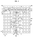
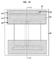
図1〜3は、本発明の一実施形態による超小型電子パッケージ又は超小型電子アセンブリ100のいくつかの図である。図1に示しているように、超小型電子アセンブリ100は、基板102の上にある2つの超小型電子素子を有している。これらの超小型電子素子は下向きに積み重ねられており、第1の超小型電子素子136の背面138(図2A)に、第2の超小型電子素子153の少なくとも一部が重なっている。
1-3 are several views of a microelectronic package or
第1の超小型電子素子136及び第2の超小型電子素子153を基板102上に配置して、第1の超小型電子素子136の外縁部(すなわち、第1の縁部144、第2の縁部145、第3の縁部146、第4の縁部147)と第2の超小型電子素子153の外縁部(すなわち、第1の縁部161、第2の縁部162、第3の縁部163、第4の縁部164)とが基板102の第1の面104上に位置し、両外縁部が基板102の周縁部を越えないようにすることができる。
A first
特定の実施形態では、基板は、高分子材料、又はセラミック若しくはガラス等の無機材料等の種々のタイプの構成体からなる誘電性要素とすることができる。基板は、その上に端子及びリード部等の導電性要素、例えば、トレース、基板コンタクト、又は端子と電気的に接続される他の導電性要素を有している。別の例では、基板は、シリコンのような半導体材料から基本的になることができるか、又は代替的に半導体材料層と、1以上の誘電性層とを含むことができる。更に別の実施形態では、基板はリード部を有するリードフレームとすることができ、端子は、リード部の端部といったリード部の一部とすることができる。 In certain embodiments, the substrate can be a dielectric element comprised of various types of constructs, such as polymeric materials or inorganic materials such as ceramic or glass. The substrate has conductive elements such as terminals and leads thereon, for example, traces, substrate contacts, or other conductive elements that are electrically connected to the terminals. In another example, the substrate can consist essentially of a semiconductor material such as silicon, or alternatively can include a semiconductor material layer and one or more dielectric layers. In yet another embodiment, the substrate can be a lead frame having a lead portion and the terminal can be part of a lead portion, such as an end of the lead portion.
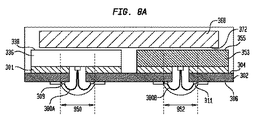
図2A及び図2Bに最もよく示しているように、基板102は、第1の面104と、該第1の面とは反対に位置する第2の面106とを有している。第1の面及び第2の面はそれぞれ、第1の横方向D1及び第2の横方向D2に広がりを有している。基板102の厚みは適用例によって異なるものの、基板102の厚さは最も一般的には、約10マイクロメートル(ミクロン)〜約100マイクロメートルである。基板102は、その表面に露出した、導電性トレース108と、端子コンタクト110、第1の組のコンタクト109、第2の組のコンタクト111といった複数のコンタクトとを有するものとすることができる。本明細書において、導電性要素がある構造体の表面「において露出している」という表現は、その表面に垂直な方向に、その構造体の外部からその表面に向かって移動する仮想的な点と接触するために、その導電性要素が利用できることを意味する。したがって、構造体の表面において露出する端子又は他の導電性要素は、そのような表面から突出している場合もあるし、そのような表面と同一平面をなす場合もあるし、そのような表面よりも奥まって位置し、構造体内の穴又は凹部を通して露出している場合もある。
As best shown in FIGS. 2A and 2B, the
図1Aに示しているように、基板102の第1の面104は向かい合った一対の縁部間に3つの部分を有することができ、これらの部分は基板102の第1の縁部103と第2の縁部105との間の、基板102の幅を分割している。3つの部分は、同じ幅又は異なった幅とすることができ、基板102の第1の縁部103に隣接する第1の外側部分900と、基板102の第2の縁部105に隣接する第2の外側部分902と、第1の外側部分900と第2の外側部分902との間のエリアを占める中央部分906とを含むことができる。一実施形態では、基板102の第2の面106上のこれらの部分のうちの1以上において、導電性トレース108及び複数のコンタクトが露出している。他の実施形態では、導電性トレース108及びコンタクトは、基板102の第1の面104及び第2の面106の両方の上に、又は基板102の内部に広がりを有している場合がある。
As shown in FIG. 1A, the
導電性トレース108は任意の導電性材料から形成することができるが、最も一般的には、銅、銅合金、金又はこれらの材料の組み合わせから形成される。トレースの厚みも適用例によって異なるものの、通常は約5ミクロン〜約25ミクロンである。基板102及びトレース108は、同時係属の、同じ譲受人に譲渡された米国特許第7,462,936号に開示されているようなプロセスによって作製することができ、その開示内容は引用することにより本明細書の一部をなすものとする。
図1、図1A、図2B及び図3に示しているように、基板102は、基板102の第1の面104と第2の面106との間に広がりを有する少なくとも2つのアパーチャ又は開口部を更に有するものとすることができる。第1の開口部116は、基板102の中央領域906(図1A)に位置決めすることができ、一対の短い縁部118と、短い縁部118の長さより長い長さを有する一対の長い縁部120とを有するものとすることができる。第1の開口部116は第1の方向D1に広がりを有するものとすることができる。第2の開口部126は、第1の方向D1と交差する第2の方向D2に広がりを有するものとすることができる。この実施形態では、第2の開口部126が広がりを有する第2の方向D2は、第1の開口部116が広がりを有する第1の方向D1に対して垂直とすることができ、それにより、第1の開口部116及び第2の開口部126はT字形を形成することができる。あるいは、第1の開口部116及び第2の開口部126をともに接合し、1つの連続した開口部を形成することができることは理解されたい。別の代替的実施形態では、第1の開口部116又は第2の開口部126はそれぞれ複数の開口部から構成することができ、それにより、第1の開口部116は第1の方向D1に広がりを有する複数の開口部を含み、第2の開口部126は、第1の方向D1と交差する第2の方向D2に広がりを有する複数の開口部を含む。開口部は、任意の代替的な形状又は配置を有することもできることを更に理解されたい。
As shown in FIGS. 1, 1A, 2B, and 3, the
一例において、第1の開口部116は、短い寸法A2より長い、長い寸法A1を有することができ、長い寸法A1は第1の方向D1に広がりを有し、短い寸法A2は第2の方向D2に広がりを有する。第2の開口部126は短い寸法B2より長い、長い寸法B1を有することができ、長い寸法B1は第2の方向D2に広がりを有し、短い寸法B2は第1の方向D1に広がりを有する。
In one example, the
図2A及び図2Bに示しているように、第1の超小型電子素子136は前面140を有している。この前面は、基板102の第1の面104に面し、接着剤101等の既知の結合材料又は手法を用いて基板102の第1の面104に取り付けることができる。第1の超小型電子素子136は、前面140の反対側に位置する背面138を更に含む。この実施形態では、前面140は、その上にボンドパッド142を有する、超小型電子素子136の第1の面であり、背面138は超小型電子素子136の背面である。この実施形態では、第1の超小型電子素子136の対向する第1の縁部144及び第2の縁部145と、対向する第3の縁部146及び第4の縁部147とは、基板102の第1の面104と第2の面106との間に広がっている。第1の超小型電子素子136の縁部は、同じ長さ又は異なった長さからなることができる。
As shown in FIGS. 2A and 2B, the first
図1Bに示しているように、第1の超小型電子素子136は任意のタイプの半導体チップとすることができる。本実施形態では、第1の超小型電子素子136は、その上に導電性要素を有するDRAM(ダイナミックランダムアクセスメモリ)チップとすることができる。図示しているように、第1の超小型電子素子136の前面140の表面積は、第1の超小型電子素子の第1の縁部と第2の縁部との間の方向に沿って幅が実質的に等しい3つの領域、すなわち、第1の外側領域920と、第2の外側領域922と、第1の外側領域920と第2の外側領域922との間に位置する中央領域924とに分けることができる。例えば、長縁部間の長さが6ミクロンである場合は、第1の外側領域と第2の外側領域と中央領域との各々の長さは2ミクロンとすることができる。それにより、中央領域924は、第1の縁部144から2ミクロンをおいて、そして第2の縁部145から2ミクロンをおいて位置することになる。つまり、中央領域は、第1の超小型電子素子136の中央3分の1に位置したものとすることができる。本明細書における超小型電子素子のいずれか又は全てがそれぞれ、メモリ記憶アレイ機能を提供する能動デバイスを他の任意の機能よりも数多く有することができる。
As shown in FIG. 1B, the first
DRAMチップに関して一般的であるように、導電性要素には、第1の超小型電子素子136の前面140の中央領域924に沿って広がりを有する複数個の第1のボンドパッド142が含まれうる。導電性要素は、第1の超小型電子素子136と、基板102の第2の面106上に位置する第1の組のコンタクト109との間の電気的接続を提供するものである。接着剤101を用いて、第1の超小型電子素子136を基板102に取り付けることができる。
As is common for DRAM chips, the conductive element may include a plurality of
図2A及び図2Bに示しているように、第1の超小型電子素子136のボンドパッド142は、基板102の第1の開口部117の真上に位置決めすることができる。これにより、ボンドパッド142は、第1の開口部117を通じて露出させることができるようになる。ボンドパッド142は、電気的接続を確立する任意の既知の方法を用いて、基板102の第2の面106上にある第1の組のコンタクト109に電気的に接続することができる。一実施形態では、ボンドワイヤ148が、第1の超小型電子素子136上のボンドパッド142から、第1の開口部116を通って、基板102の第2の面106上にある第1の組のコンタクト109まで延びたものとすることができる。トレース108(図3)を用いて、第1の組のコンタクト109を端子コンタクト110に接続することができる。
As shown in FIGS. 2A and 2B, the
第2の超小型電子素子153は、第1の超小型電子素子136と同様のものとすることができる。ボンドパッドをその上に有する第2の超小型電子素子の前面157は、第1の超小型電子素子136に面することで、第2の超小型電子素子153は第1の超小型電子素子136の背面138の上に重なっている。図1Cに示しているように、本実施形態における第2の超小型電子素子153は、向かい合った第1の縁部161及び第2の縁部162と、第2の超小型電子素子153の背面155と前面157との間に広がりを有するとともに第1の縁部161及び第2の縁部162に隣接する、向かい合った第3の縁部163及び第4の縁部164とを有している。ボンドパッド159等の導電性要素が、第2の超小型電子素子153の前面157に沿って広がりを有している。本実施形態では、第2の超小型電子素子153は、DRAMチップ等の半導体チップとすることができ、ボンドパッド159が第2の超小型電子素子153の中央領域932に沿って位置している。中央領域932は、第1の外側領域928と第2の外側領域930との間に位置している。一実施形態では、ボンドパッド159は、第1の超小型電子素子136上のボンドパッド142が広がりを有する方向と交差する方向に広がりを有するものとすることができる。
The second
図1Bに示しているように、特定の例では、第1の超小型電子素子136は、第1の超小型電子素子の前面140の中央領域924において方向D3に広がりを有する5つ以上のボンドパッド142からなる少なくとも1つの列142’を有することができる。また、図1Cに示しているように、一例において、第2の超小型電子素子153は、第2の超小型電子素子の前面157の中央領域932において方向D4に広がりを有する5つ以上のボンドパッド159からなる少なくとも1つの列159’を有することができる。図3の例に示しているように、ボンドパッド142の列142’が広がる方向D3は、ボンドパッド159の列159’が広がる方向D4と交差したものとすることができる。図3に示しているように、方向D3は、第1の開口部116の長手寸法の方向D1に平行とすることができ、方向D4は、第2の開口部126の長手寸法の方向D2に平行とすることができるが、そうでなくてもよい。例えば、一実施形態では(不図示)、方向D3は、第1の窓の短い寸法が広がる方向D2に平行とすることができ、方向D4は、第2の窓の短い寸法が広がる第1の方向D1に平行とすることができる。
As shown in FIG. 1B, in a particular example, the first
図2Bに示しているように、第2の超小型電子素子153は第1の超小型電子素子136の上方に位置したものとすることができる。図示しているように、第1の超小型電子素子136よりも上の高さで第2の超小型電子素子153を支持するために、基板102と第2の超小型電子素子153との間にスペーサ135を設けることができる。図1に最もわかりやすく示しているように、第2の超小型電子素子153の第1の縁部161及び第2の縁部162は、第1の超小型電子素子136の第1の縁部144及び第2の縁部145と交差する方向に広がったものとすることができる。その結果、第2の超小型電子素子153における第1の縁部161及び第2の縁部162は、第1の超小型電子素子136における第3の縁部146及び第4の縁部147の一方を越えて広がっている。
As shown in FIG. 2B, the second
図2Bに示しているように、第2の超小型電子素子153におけるボンドパッド159は、基板102において露出した複数のコンタクトのうちの第2の組のコンタクト111と電気的に接続することができる。
As shown in FIG. 2B, the
導電性要素を用いて、第1の超小型電子素子136上のボンドパッド159を、基板102の第2の面106における第2の組のコンタクト111と電気的に接続することができる。本実施形態では、ボンドワイヤ165を用いて、第2の超小型電子素子153上のボンドパッド159を、基板102の第2の面106上の第2の組のコンタクト111(図2B〜図3)と接続することができる。図示しているように、ボンドワイヤ165は、第2の開口部126を通って延び、第2の組のコンタクト111に接続する。
A conductive element can be used to electrically connect the
図2Aに示しているように、スタックアセンブリが組み立てられると、基板102の第1の面104と第1の超小型電子素子136と第2の超小型電子素子153とのうちのいくつか又は全ての上に封止材199を設けることができる。この封止材は、第1の開口部116及び第2の開口部126の各々を通って延びているボンドワイヤ148、165を覆うことができる。
As shown in FIG. 2A, when the stack assembly is assembled, some or all of the
図3に示しているように、基板102の第2の面106において露出する端子コンタクト110(図2B)に、はんだボール115のアレイを取り付けることができる。図示しているように、トレース108が第1の組のコンタクト109から第2の面106に沿って延び、第1の組のコンタクト109とハンダボール115を支持する端子コンタクト110との間の電気的接続を提供することができる。端子110は、超小型電子アセンブリ100を該アセンブリの外部にある少なくとも1つの要素に接続するためのものとすることができる。
As shown in FIG. 3, an array of
特定の例では、基板102は、第1の面104と第2の面106との間において第2の方向D2に広がりを有する第1の周縁部3も有することができる。また、基板102は、第1の面104と第2の面106との間において第1の方向D1に広がりを有する第2の周縁部103も有することができる。さらに、基板102は、第2の周縁部103の反対側に位置し、第1の面104と第2の面106との間において第1の方向D1に広がりを有する第3の周縁部105も有することができる。
In a particular example, the
第1の開口部116は、第2の開口部126と第1の周縁部3との間に設けることができ、第1の方向D1に広がりを有する長手の第1の寸法L1と、該第1の寸法より小さな、第2の方向D2に沿った第2の寸法W1とを有することができる。第2の開口部126は、第2の方向D2に広がりを有する長手の第1の寸法L2と、該第1の寸法より小さな、第1の方向D1に沿った第2の寸法W2とを有することができる。
The
基板102は、第1の周縁部3と第1の開口部116との間に広がる、第2の面106上の第1の周辺領域P1を有することができる。また、基板102は、第2の周縁部103と第2の開口部126との間に広がる、第2の面106上の第2の周辺領域P2も有することができる。さらに、基板102は、第3の周縁部105と第2の開口部126との間に広がる、第2の面106上の第3の周辺領域P3も有することができる。第2の周辺領域P2及び第3の周辺領域P3は、第2の開口部126の両側に位置したものとすることができる。
The
図3に示しているように、第1の方向D1に沿って端子110のうちの少なくとも1つ、例えば第1の端子110aを通る直線S1が第1の開口部116を通るか又はその上方を通るものとなるように、前記第1の端子110aを第1の周辺領域P1内に少なくとも部分的に配置することができる。また、第2の方向D2に沿って端子110のうちの少なくとも1つ、例えば第2の端子110bを通る直線S2が第2の開口部126を通るか又はその上方を通るものとなるように、前記第2の端子を第2の周辺領域P2内に少なくとも部分的に配置することができる。さらに、第2の方向D2に沿って端子110のうちの少なくとも1つ、例えば第3の端子110cを通る直線が第2の開口部126を通るか又はその上方を通るものとなるように、前記第3の端子を第3の周辺領域P3内に少なくとも部分的に配置することができる。特定の例では、同一直線S2が第2の端子110b及び第3の端子110cを通るものとすることができるが、そうでなくてもよい。
As shown in FIG. 3, a straight line S1 passing through at least one of the
本明細書において説明する他の実施形態は、図1〜図3の実施形態に実質的に類似している。各実施形態は、基板、及び基板内の各開口部の上方において超小型電子素子が前面を下にした姿勢、すなわち下向きの配置で設けられる方法に関してのみ異なる。そのため、図1〜図3の実施形態に関して開示した原理は、本明細書において開示する他の実施形態にも同じく適用することができる。したがって、同様の要素を説明するために同様の符号を用いる。 Other embodiments described herein are substantially similar to the embodiment of FIGS. Each embodiment differs only in the substrate and the way in which the microelectronic elements are provided in a position with the front side down above each opening in the substrate, ie in a downward arrangement. As such, the principles disclosed with respect to the embodiments of FIGS. 1-3 are equally applicable to other embodiments disclosed herein. Accordingly, like reference numerals are used to describe like elements.
図3A及び図3Bに示しているように、超小型電子アセンブリ100’は図1〜図3に関して図示及び説明した超小型電子アセンブリに類似している一方で、第1の開口部16及び第2の開口部26がそれぞれ、第1の方向D1に沿ったそれぞれの長手の第1の寸法L1及びL2と、第2の方向に沿ったそれぞれの第2の寸法W1及びW2とを有しているという点で異なっている。すなわち、第1の開口部16及び第2の開口部26は、互いに交差しているのではなく、互いに平行に延びている。
As shown in FIGS. 3A and 3B, the
図3Aからわかるように、図1〜図3と同様、第1の超小型電子素子36は、基板2における第1の面4に面する前面40と、該前面にあり、第1の開口部16と位置合わせされているボンドパッド42と、前面の反対側に位置する背面38と、前面と背面との間に延びている縁部46とを有している。第2の超小型電子素子53は、第1の超小型電子素子36の背面38に面し、第1の超小型電子素子の縁部46を越えて突出した前面57と、第2の超小型電子素子の前面にあり、第2の開口部26と位置合わせされているボンドパッド59とを有している。
As can be seen from FIG. 3A, as in FIGS. 1 to 3, the first
特定の例では、第1の超小型電子素子36は、前面と背面との間に延びている縁部46と、反対側に位置する縁部との間にある幅を有するものとすることができる。第2の超小型電子素子53は、前面と背面との間にそれぞれ延びている、向かい合った縁部間にある幅を有するものとすることができる。第1の超小型電子素子36の幅は第1の開口部16の第2の寸法W1よりも大きくすることができる。第2の超小型電子素子53の幅は、第2の開口部26の第2の寸法W2よりも大きくすることができる。
In a particular example, the first
基板2における第2の面6において露出している端子コンタクト10に、はんだボール15のアレイを取り付けることができる。第1の組のコンタクト9及び第2の組のコンタクト11から第2の面6に沿ってトレースが延びており、基板コンタクト9、11とはんだボール15を支持する端子コンタクト10との間の電気的接続を提供することができる。第1の超小型電子素子36及び第2の超小型電子素子53それぞれのボンドパッド42、59は、基板2の導電性要素(例えば、基板コンタクト9、11及び端子10)と電気的に接続することができる。端子10は、超小型電子アセンブリ100’を、該アセンブリの外部にある少なくとも1つの要素に接続するように構成することができる。
An array of
特定の例では、基板2は、第1の面4と第2の面6との間において第2の方向D2にそれぞれ延びている、向かい合った第1の周縁部3及び第2の周縁部5を有するものとすることができる。基板2は、第1の周縁部3と、第1の開口部16及び第2の開口部26の各々との間に広がっている、第2の面6における第1の周辺領域P1及び第2の周辺領域P2を有するものとすることができる。また、基板2は、第2の周縁部5と、第1の開口部16及び第2の開口部26の各々との間に広がっている、第2の面6における第3の周辺領域P3及び第4の周辺領域P4をも有するものとすることができる。第1の周辺領域P1及び第3の周辺領域P3は、第1の開口部16の両側に位置するものとすることができる。第2の周辺領域P2及び第4の周辺領域P4は、第2の開口部26の両側に位置するものとすることができる。
In a particular example, the
図3Bに示しているように、第1の開口部16は、第1の周縁部3から第2の開口部26と同じ距離を置いた位置まで延びているとともに、第2の周縁部5から第2の開口部と同じ距離を置いた位置まで延びているが、そうでなくてもよい。一例では、第1の開口部16及び第2の開口部26のうちの一方は、他方に比べて、周縁部3及び5のうちの一方又は両方に近い位置まで延びたものとすることができる。
As shown in FIG. 3B, the
図3Bに示しているように、端子10のうちの少なくとも1つ、例えば第1の端子10aは、第1の方向D1に沿って当該第1の端子10aを通る直線S1が第1の開口部16を通るか又はその上方を通るものとなるように、第1の周辺領域P1内に少なくとも部分的に配置することができる。また、端子10のうちの少なくとも1つ、例えば第2の端子10bは、第1の方向D1に沿って当該第2の端子を通る直線S2が第2の開口部26を通るか又はその上方を通るものとなるように、第2の周辺領域P2内に少なくとも部分的に配置することができる。
As shown in FIG. 3B, at least one of the
端子10のうちの少なくとも1つ、例えば第3の端子10cは、第2の方向D3に沿って当該第3の端子を通る直線が第1の開口部16を通るか又はその上方を通るものとなるように、第3の周辺領域P3内に少なくとも部分的に配置することができる。また、端子10のうちの少なくとも1つ、例えば第4の端子10dは、第1の方向D1に沿って当該第4の端子を通る直線が第2の開口部26を通るか又はその上方を通るものとなるように、第4の周辺領域P4内に少なくとも部分的に配置することができる。特定の例では、同一直線S1が第1の端子10a及び第3の端子10cを通って延びるものとすることができるが、そうでなくてもよい。一実施形態では、同一直線S2が第2の端子10b及び第4の端子10dを通って延びるものとすることができるが、そうでなくてもよい。
At least one of the
一例では、第1の超小型電子素子36のボンドパッド42は、第1の開口部16と位置合わせされた部分を有する第1のリード部48により、導電性要素9に電気的に接続することができる。同様に、第2の超小型電子素子53のボンドパッド59は、第2の開口部26と位置合わせされた部分を有する第2のリード部65により、導電性要素11に電気的に接続することができる。一実施形態においては、例えば第1のリード部48がリードボンド部(lead bond)である場合には、第1のリード部は第1の開口部16内で延びていない場合がある。同様に、例えば第2のリード部65がリードボンド部である場合には、第2のリード部は第2の開口部26内で延びていない場合がある。
In one example, the bond pad 42 of the first
図3Aに示しているように、第1の超小型電子素子36のボンドパッド42は、第1の開口部16を通じて延びているワイヤボンド部48によって導電性要素9に電気的に接続することができる。同様に、第2の超小型電子素子53のボンドパッド59は、第2の開口部26を通じて延びているワイヤボンド部65によって導電性要素11に電気的に接続することができる。特定の例では、第1のワイヤボンド部48は第1の開口部16のみを通って延びているものとすることができ、第2のワイヤボンド部は第2の開口部26のみを通って延びているものとすることができる。
As shown in FIG. 3A, the bond pad 42 of the first
例示的な実施形態では、第1の超小型電子素子36及び第2の超小型電子素子53は、図1B及び図1Cに示したものと同じように構成されるそれぞれのボンドパッド42及び59を有することができる。このような例では、第1の超小型電子素子36及び第2の超小型電子素子53はそれぞれ、各々の前面40、57の中央領域において第1の方向に広がりを有する、それぞれのボンドパッド42、59のうちの5つ以上のボンドパッドを有する少なくとも1つの列を有することができる。各中央領域は、それぞれの超小型電子素子の向かい合った第1の縁部と第2の縁部との間の距離の中央3分の1に広がっている。
In the exemplary embodiment, the first
図3Cは、図3Aの超小型電子アセンブリ100の別の可能性としての底面図である。図3Cに示している実施形態では、基板2は、間隔を置いて配置され、かつ互いに隣接して配置された第1の誘電性要素2a及び第2の誘電性要素2bを有するものとすることができる。各誘電性要素は向かい合った上面及び底面を有している。2つの誘電性要素2a及び2bは互いに同一平面に設けることができる。それにより、基板2における第1の面4は両誘電性要素の上面を含んだものとすることができ、基板における第2の面6は両誘電性要素の底面を含んだものとすることができる。
FIG. 3C is a bottom view of another possibility of the
別の例では、図3Cに示した誘電性要素2a及び2b等の、本明細書に記載の誘電性要素のいずれか又はそれぞれを、シリコン等の半導体材料から基本的になる基板要素へとそれぞれ置き換えることができる。特定の実施形態では、本明細書に記載の誘電性要素のいずれか又はそれぞれを、半導体材料層と1以上の誘電性層とを含むことのできる基板要素へとそれぞれ置き換えることができる。更に別の実施形態では、本明細書に記載の誘電性要素のいずれか又はそれぞれを、リード部を有するリードフレームにそれぞれ置き換えることができる。リード部の端部といったリード部の一部を端子とすることができる。
In another example, any or each of the dielectric elements described herein, such as
第1の誘電性要素2a及び第2の誘電性要素2bの、隣接しているとともに向かい合っている縁部102a及び102b間の空間によって第1の開口部16cを形成することができる。隣接しているとともに向かい合っている縁部102a及び102bはそれぞれ、第1の寸法L1を有するものとすることができ、それぞれが第1の方向D1に沿ったものとすることができる。第1の開口部16cは、第1の寸法L1よりも小さな、第2の方向D2に沿った第2の寸法W1を有するものとすることができる。第2の開口部26は図3Bと同様にすることができ、それにより、第2の開口部は第2の誘電性要素2bによって囲まれたものとすることができる。
The
図3Bに示した実施形態と同様に、端子10のうちの少なくとも1つ、例えば第1の端子10aは、第1の方向D1に沿って当該第1の端子10aを通る直線S1が第1の開口部16cを通るか又はその上方を通るものとなるように、第1の周辺領域P1内に少なくとも部分的に配置することができる。端子10のうちの少なくとも1つ、例えば第2の端子10bは、第1の方向D1に沿って当該第2の端子を通る直線S2が第2の開口部26を通るか又はその上方を通るものとなるように、第2の周辺領域P2内に少なくとも部分的に配置することができる。同様に、少なくとも1つの第3の端子10c及び第4の端子10dは、図3Bに関して上記で説明したように、第3の周辺領域及び第4の周辺領域内に少なくとも部分的に配置することができる。
Similar to the embodiment shown in FIG. 3B, at least one of the
特定の例では、第2の開口部26は、第1の開口部16cに対して垂直方向のものとすることができる。例えば、第2の開口部26は、第2の方向D2に沿った第1の寸法L2と、該第1の寸法よりも小さな、第1の方向D1に沿った第2の寸法W2とを有するものとすることができる。一実施形態において、基板2は、第1の誘電性要素2a及び第2の誘電性要素2bの、隣接しているとともに向かい合った縁部102a及び102bの間に広がりを有する誘電性領域Rをも含んだものとすることができる。該基板の第1の面は該誘電性領域の上面を含んでおり、第2の面は該誘電性領域の底面を含む。特定の例では、誘電性領域Rは、基板の平面において、誘電性要素2a、2bよりも大きなヤング率を有するものとすることができる。
In a particular example, the
図3A及び図3Cに示しているように、第1の超小型電子素子36は第1の開口部16cの上に重なったものとすることができ、第2の超小型電子素子53は第2の開口部26の上に重なったものとすることができ、基板2により近い超小型電子素子は第1の開口部の上に重なっている超小型電子素子である。しかし、そうでなくてもよい。別の実施形態では、基板2により近い超小型電子素子(例えば第1の超小型電子素子36)が第2の開口部26の上に重なったものとすることができ、基板からより離れている超小型電子素子(例えば第2の超小型電子素子53)が第1の開口部16cの上に重なったものとすることができる。
As shown in FIGS. 3A and 3C, the first
図3Dは、図3Aの超小型電子アセンブリ100の別の可能性としての底面図である。図3Dに示している実施形態では、基板2は、間隔を置いて配置され、かつ互いに隣接して配置された第1の誘電性要素2aと第2の誘電性要素2bと第3の誘電性要素2cとを含むことができる。各誘電性要素は向かい合った上面及び底面を有している。3つの誘電性要素2a、2b、2cは互いに同一平面に設けることができ、それにより、基板2における第1の面4は3つ全ての誘電性要素の上面を含んだものとすることができ、基板における第2の面6は3つ全ての誘電性要素の底面を含んだものとすることができる。
FIG. 3D is a bottom view of another possibility of the
第1の誘電性要素2a及び第2の誘電性要素2bの、隣接しているとともに向かい合っている縁部間の空間により、図3Cの第1の開口部16cに類似した第1の開口部16dを形成することができる。また、第2の誘電性要素2b及び第3の誘電性要素2cの、隣接しているとともに向かい合っている縁部間の空間により、第2の開口部26dを形成することができる。
A
図3Cに示した実施形態と同様、端子10のうちの少なくとも1つ、例えば第1の端子10aは、第1の方向D1に沿って当該第1の端子10aを通る直線S1が第1の開口部16dを通るか又はその上方を通るものとなるように、第1の周辺領域P1内に少なくとも部分的に配置することができる。端子10のうちの少なくとも1つ、例えば第2の端子10bは、第1の方向D1に沿って当該第2の端子を通る直線S2が第2の開口部26dを通るか又はその上方を通るものとなるように、第2の周辺領域P2内に少なくとも部分的に配置することができる。同様に、少なくとも1つの第3の端子10c及び第4の端子10dは、図3Bに関して上記で説明したように、第3の周辺領域及び第4の周辺領域内に少なくとも部分的に配置することができる。
Similar to the embodiment shown in FIG. 3C, at least one of the
一例では、端子10は、第1の誘電性要素2aと第2の誘電性要素2bと第3の誘電性要素2cとの各底面において露出した第1の端子と第2の端子と第3の端子とを含んだものとすることができる。超小型電子素子36、53のうちの少なくとも1つの超小型電子素子のボンドパッド42、59のうちの少なくとも幾つかは、第1の基板部分、第2の基板部分、第3の基板部分のそれぞれの第1の端子、第2の端子、第3の端子のうちの2以上と電気的に接続することができる。特定の実施形態において、第1の超小型電子素子36のボンドパッド42のうちの少なくとも幾つかは、第1の基板部分2a及び第2の基板部分2bの端子10に電気的に接続することができる。一実施形態では、第2の超小型電子素子53のボンドパッド59のうちの少なくとも幾つかは、第2の基板部分2b及び第3の基板部分2cの端子10に電気的に接続することができる。
In one example, the terminal 10 includes the first terminal, the second terminal, and the third terminal exposed on the bottom surfaces of the first
図3E、図3F、図3Gはそれぞれ、図3Aの超小型電子アセンブリ100の代替的可能性としての底面図である。図3Eの実施形態は図3Dに示した実施形態と類似しているが、各周辺領域が第1の方向D1に沿って互いに隣接して配置された複数の端子10を含みうる点で異なる。例えば、周辺領域P1は端子10a及び10a’を含み、第1の開口部16eと基板2の周縁部との間において第1の方向に延びる直線S1は端子10a及び10a’の両方を通って延びている。
3E, 3F, and 3G are bottom views of alternative possibilities for the
図3Fに示している実施形態は図3Dに示した実施形態と類似しているが、周辺領域が第2の基板部分2b上ではなく、第1の基板部分2a上及び第3の基板部分2c上に位置している点で異なる。図3Gに示している実施形態は、図3Fに示した実施形態と類似しているが、第2の基板部分2bがその中央部分において、その周辺部分における第2の幅W’よりも大きい第1の幅Wを有している点で異なる。両周辺部分は第1の方向D1に沿って中央部分と隣接している。
The embodiment shown in FIG. 3F is similar to the embodiment shown in FIG. 3D, but the peripheral region is not on the
図3Hは、図3Dに示した超小型電子アセンブリ100’を複数備えたアセンブリの製造途中の状態を示している。図3Hは、第1の超小型電子アセンブリ100a’と第2の超小型電子素子100b’とを示している。第1及び第2の超小型電子アセンブリ100は、基板部分2a、2b、2cにおける隣接した基板部分同士を接合する、基板2の接続部分2’により接合されている。例えば、基板2の接続部分2’は、第1及び第2の超小型電子アセンブリの各々の第1の基板部分2a同士と、両超小型電子アセンブリの各々の第2の基板部分2b同士と、両超小型電子アセンブリの各々の第3の基板部分2c同士とを接合する。超小型電子アセンブリ100’の各超小型電子アセンブリを製造した後に、接続部分2’を、例えば、個々の超小型電子アセンブリをダイシングし、それにより分けることによって、超小型電子アセンブリから除去することができる。
FIG. 3H illustrates a state in the middle of manufacturing an assembly including a plurality of
図3A〜図3Hにおいて、第1の開口部及び第2の開口部は、互いに平行なものとして示しているが、他の実施形態では、図3A〜図3Hに示した実施形態の任意の実施形態における第1の開口部及び第2の開口部は、例えば、図1に示したように、互いに交差するように方向づけることができる。そのような実施形態において、第1の開口部及び第2の開口部の一方を、基板の誘電性要素によって囲まれるようにすることができ、他方の開口部は、第1の誘電性要素及び第2の誘電性要素の、隣接しているとともに向かい合った縁部間の空間により形成することができる。特定の例では、第1の開口部及び第2の開口部はいずれも、隣接する誘電性要素の、隣接しているとともに向かい合った縁部間のそれぞれの空間により形成することができる。 In FIGS. 3A-3H, the first opening and the second opening are shown as being parallel to one another, but in other embodiments, any implementation of the embodiment shown in FIGS. 3A-3H. The first opening and the second opening in the form can be oriented to intersect each other, for example, as shown in FIG. In such an embodiment, one of the first opening and the second opening may be surrounded by a dielectric element of the substrate, the other opening being the first dielectric element and The second dielectric element can be formed by a space between adjacent and opposite edges. In a particular example, both the first opening and the second opening can be formed by respective spaces between adjacent and facing edges of adjacent dielectric elements.
図3A〜図3Hにおいて、超小型電子アセンブリは2つの超小型電子素子を有するものとして示しているが、他の実施形態では、図3A〜図3Hに示した超小型電子アセンブリの任意の超小型電子アセンブリが、第3の超小型電子素子、又は第3及び第4の超小型電子素子を含んでいてもよい。例えば、図6、図9、図12に示している実施形態は、互いに隣接して配置される、2つ、3つ、4つ、5つ又は任意のその他の数の、間隔を置いて配置される誘電性要素を有する基板を含んだものとすることができる。 3A-3H, the microelectronic assembly is shown as having two microelectronic elements, but in other embodiments, any microminiature of the microelectronic assembly shown in FIGS. 3A-3H. The electronic assembly may include a third microelectronic element, or third and fourth microelectronic elements. For example, the embodiments shown in FIGS. 6, 9, and 12 may be two, three, four, five, or any other number of spaced apart, positioned adjacent to each other. It may include a substrate having a dielectric element to be made.
特定の例では、図3A〜図3Hに示した超小型電子素子及び開口部の構成の任意の構成を、単一の超小型電子アセンブリ内で互いに隣接するように繰り返し設けることができる。例えば、図3Iに示しているように、図3Aの超小型電子素子の構成を繰り返し設けることができる。その結果、単一の基板2iは、4つの開口部16、26、32及び82と、部分的に重なり合った超小型電子素子の2つのペアとを有することができる。そのため、重なり合った超小型電子素子36及び53の第1のペアが、2つの第1開口部16及び26の上に重なったものとすることができるとともに、前記第1のペアに隣接する、重なり合った超小型電子素子68及び88の第2のペアが、2つの第2開口部32及び82の上に重なったものとすることができる。
In particular examples, any of the microelectronic element and aperture configurations shown in FIGS. 3A-3H can be repeatedly provided adjacent to each other within a single microelectronic assembly. For example, as shown in FIG. 3I, the configuration of the microelectronic element of FIG. 3A can be repeatedly provided. As a result, a single substrate 2i can have four
一例では、図3Iにおける第4の超小型電子素子88を省くことができる。そして、超小型電子アセンブリが、部分的に重なり合った3つの超小型電子素子を有するものとなるようにすることができる。3つの超小型電子素子のうちの2つは、それらの前面が基板の面と平行な単一の平面内に存在するように配置され、その他の超小型電子素子は、基板の面と平行な別の平面に位置する前面を有している。 In one example, the fourth microelectronic element 88 in FIG. 3I can be omitted. The microelectronic assembly can then have three microelectronic elements partially overlapping. Two of the three microelectronic elements are arranged such that their front faces lie in a single plane parallel to the plane of the substrate, and the other microelectronic elements are parallel to the plane of the substrate. It has a front face located in another plane.
図3Iの実施形態は、種々の底面構造とすることができる。一例では、図3Jに示すように、図3Bに示した構成を繰り返し設け、単一の基板2jが、該基板によってそれぞれ囲まれている4つの平行な開口部16j、26j、32j及び82jを有するものとなるように、そして、複数の超小型電子素子のうちの対応する一超小型電子素子のコンタクトが各開口部16j、26j、32j及び82jと位置合わせされるようにすることができる。別の例では、図3Kに示すように、図3Dに示した構成を繰り返し設け、単一の基板2kが互いに間隔を置いて配置された5つの誘電性要素2a、2b、2c、2d及び2eを有するものとなるように、そして、複数の超小型電子素子のうちの対応する一超小型電子素子のコンタクトが各開口部16k、26k、32k及び82kと位置合わせされるようにすることができる。各開口部は、複数の誘電性要素のうちの隣り合った誘電性要素の隣接し、向かい合った縁部間の開口によって形成されている。他の実施形態では、図3J及び図3Kの基板の構造を組み合わせて一つの実施形態とし、結果として、図3Iに示した4つの超小型電子素子のうちの1以上がそれぞれ、基板の誘電性要素に囲まれた開口部に重なるように、そして、図3Iに示した4つの超小型電子素子のうちの1以上がそれぞれ、複数の誘電性要素のうちの隣り合った誘電性要素の隣接し、向かい合った縁部間の開口により形成される開口部に重なるようにすることができる。
The embodiment of FIG. 3I can have various bottom structures. In one example, as shown in FIG. 3J, the configuration shown in FIG. 3B is repeated, and a single substrate 2j has four
図4〜図6は、前面を下にして積み重ねられた3つの超小型電子素子を備えた、代替的なスタック型超小型電子アセンブリ200を示している。図5A及び図5Bに最も良く示しているように、第1の超小型電子素子236の上に、第2の超小型電子素子253及び第3の超小型電子素子268のいずれもが重なったものとすることができる。
4-6 illustrate an alternative stacked
図4及び図5Bに最も良く示しているように、基板202は、第1の面204及び第2の面206と、第1の面204と第2の面206との間に延びている3つの開口部とを有している。先の実施形態と同様に、第1の開口部216は第1の端部222及び第2の端部224を有し、基板202の中央部分に設けることができる。基板の中央部分は先と同様、基板の第1の縁部203と、向かい合った第2の縁部205との間において基板202の中央3分の1にある。第1の開口部216は、第1の端部222及び第2の端部224において短縁部218を有している。第2の開口部226は、第1の開口部216における第1の端部222に隣接するように設けることができる。
As best shown in FIGS. 4 and 5B, the
第3の開口部232は、第1の開口部216における第2の端部224に隣接するように設け、第3の開口部232の長縁部234が、第1の開口部216の長縁部220が延びている方向と交差する方向に延びるようにすることができる。この構成では、第2の開口部226及び第3の開口部232は、I字形となるように、互いに平行に、かつ第1の開口部216に対して垂直に設けることができる。あるいは、第1の開口部216と第2の開口部226と第3の開口部232とは、連続した1つの開口部となるように、互いに接合することができる。先の実施形態と同様に、第1の開口部216と第2の開口部226と第3の開口部232とのうちの1以上は複数の開口部から構成することができる。
The
一例では、第1の開口部216は、短い寸法A2より大きな長い寸法A1を有することができる。長い寸法A1は第1の方向D1に延び、短い寸法A2は第1の方向と交差する第2の方向D2に延びている。第2の開口部226は、短い寸法B2より大きな長い寸法B1を有することができる。長い寸法B1は第2の方向D2に延び、短い寸法B2は第1の方向D1に延びている。第3の開口部232は、短い寸法C2より大きな長い寸法C1を有することができる。長い寸法C1は第2の方向D2に延び、短い寸法C2は第1の方向D1に延びている。
In one example, the
第1の超小型電子素子236及び第2の超小型電子素子253は、図1〜図3の実施形態に類似の構成において積み重ねられるが、第3の超小型電子素子268が本アセンブリ内に含まれるという点で異なる。図5A及び図5Bに示しているように、第1の超小型電子素子236及び第2の超小型電子素子253は別々の平面に存在している。図5Bにおいて、よりわかりやすく示されるように、第3の超小型電子素子268は、第1の超小型電子素子236及び第2の超小型電子素子253に隣接して配置することができる。この実施形態では、第3の超小型電子素子268は、第2の超小型電子素子253と同じ平面に存在しているが、第1の超小型電子素子236と同じ平面に存在しているわけではない。図示しているように、1以上のスペーサ235を用いて、第1の超小型電子素子236の上方で第3の超小型電子素子268を支持することができる。その結果、第3の超小型電子素子268における第2の縁部277が、第1の超小型電子素子236における第4の縁部247と、第1の超小型電子素子236の第1の縁部244及び第2の縁部245の一部とに重なるか又はそれらを覆うものとなるようにすることができる。第3の超小型電子素子268におけるボンドパッド274が、第3の超小型電子素子268の中央領域942の一部に沿って延び(図5B、図6)、第3の開口部232に面している。上記で開示した実施形態と同様に、中央領域942は、第3の超小型電子素子268における第1の縁部276と第2の縁部277との間の長さの中央3分の1に位置決めすることができる。第3の超小型電子素子268上のボンドパッド274は、第3の開口部232と位置合わせされており、第3の開口部を通じて露出することができる。
The first
2つの超小型電子素子を有する実施形態に関して上記で説明したように、第3の超小型電子素子268は、当該第3の超小型電子素子の前面の中央領域においてある方向に広がりを有する5つ以上のボンドパッド274の少なくとも1つの列を有することができる。特定の例では、第3の超小型電子素子268の5つ以上のボンドパッド274の少なくとも1つの列は、当該第3の超小型電子素子の周縁部に隣接して配置することができる。図6に示しているように、第3の超小型電子素子268の5つ以上のボンドパッド274の少なくとも1つの列274’は、第2の開口部226及び第3の開口部232の長い寸法が延びうる方向と同じ方向D2に延びたものとすることができ、その方向は第1の開口部216の長い寸法が延びうる方向D1と交差するものとすることができるが、そうでなくてもよい。
As described above with respect to the embodiment having two microelectronic elements, the third
導電性接続部を用いて、各超小型電子素子上の各ボンドパッドを、基板の底面にあるそれぞれの組のコンタクトと接続することができる。例えば、図示しているように、ボンドワイヤ280は、第3の超小型電子素子268の表面に露出したボンドパッド274を、基板202の第2の面206上の第3の組のコンタクト213と接続する。そして、図6に示しているように、導電性トレース208は、第3の超小型電子素子268上の各ボンドパッド274を、はんだボールを支持する端子コンタクト210と電気的に接続することができる。端子210は、超小型電子アセンブリ200を、該アセンブリの外部にある少なくとも1つの構成要素に接続するように構成することができる。
Using the conductive connections, each bond pad on each microelectronic element can be connected to a respective set of contacts on the bottom surface of the substrate. For example, as shown,
先の実施形態と同様に、第1の超小型電子素子236、第2の超小型電子素子253及び第3の超小型電子素子268の構成によれば、第1の超小型電子素子236、第2の超小型電子素子253及び第3の超小型電子素子268の各ボンドパッド242、259、274(図5B)のそれぞれを、第1の開口部216、第2の開口部226及び第3の開口部232のそれぞれと位置合わせできるようになる。これにより、各導電性接続部が、隣接する導電性接続部からの干渉を受けることなく、第1の開口部216、第2の開口部226及び第3の開口部232内を通ることができるか、又は通り抜けることができるようになる。さらに、これにより、中央領域に配置されたボンドパッドを有する2つ以上のチップを積み重ねることができるようになる。
Similar to the previous embodiment, according to the configuration of the first
特定の例では、基板202は、第1の面204と第2の面206との間において第1の方向D1に延びる第1の周縁部203をも有することができる。また、基板202は、第1の面204と第2の面206との間において第1の方向D1に延びる第2の周縁部205をも有することができる。
In a particular example, the
第1の開口部216は、第1の方向D1に延びる長手の第1の寸法L1と、該第1の寸法より小さな、第2の方向D2に沿った第2の寸法W1とを有することができる。第2の開口部226は、第2の方向D2に沿った長手の第1の寸法L2と、該第1の寸法より小さな、第1の方向D1に沿った第2の寸法W2とを有することができる。第3の開口部232は、第2の方向D2に沿った長手の第1の寸法L3と、該第1の寸法より小さな、第1の方向D1に沿った第2の寸法W3とを有することができる。
The
基板202は、第1の周縁部203と第2の開口部226及び第3の開口部232のそれぞれとの間に広がりを有する、第2の面206における第1の周辺領域P1及び第2の周辺領域P2を有することができる。また、基板202は、第2の周縁部205と、第2の開口部226及び第3の開口部232のそれぞれとの間に広がりを有する、第2の面206における第3の周辺領域P3及び第4の周辺領域P4をも有することができる。第1の周辺領域P1及び第3の周辺領域P3は第2の開口部226の両側に設けることができ、第2の周辺領域P2及び第4の周辺領域P4は第3の開口部232の両側に設けることができる。
The
図6に示しているように、端子210のうちの少なくとも1つ、例えば第1の端子210aは、第2の方向D2に沿って当該第1の端子210aを通る直線S1が、第2の開口部226を通るか又はその上方を通るものとなるように、第1の周辺領域P1内に少なくとも部分的に配置することができる。端子210のうちの少なくとも1つ、例えば第2の端子210bは、第2の方向D2に沿って当該第2の端子を通る直線S2が、第3の開口部232を通るか又はその上方を通るものとなるように、第2の周辺領域P2内に少なくとも部分的に配置することができる。
As shown in FIG. 6, at least one of the
端子210のうちの少なくとも1つ、例えば第3の端子210cは、第2の方向D2に沿って当該第3の端子210cを通る直線が、第2の開口部226を通るか、又はその上方を通るものとなるように、第3の周辺領域P3内に少なくとも部分的に配置することができる。特定の例では、同じ直線S1が第1の端子210a及び第3の端子210cを通るものとすることができるが、そうでなくてもよい。
At least one of the
端子210のうちの少なくとも1つ、例えば第4の端子210dは、第2の方向D2に沿って当該第4の端子210dを通る直線が、第3の開口部232を通るか又はその上方を通るものとなるように、第4の周辺領域P4内に少なくとも部分的に配置することができる。特定の例では、同じ直線S2が第2の端子210b及び第4の端子210dを通るものとすることができるが、そうでなくてもよい。
At least one of the
図7〜図9には、下向きで基板の上に積み重ねられている4つの超小型電子素子を備えた超小型電子アセンブリ300を示す別の実施形態を示している。この実施形態では、4つの開口部が、基板302の第1の面304及び第2の面306を貫通して延びている。図7に最も良く示しているように、第1の開口部316及び第2の開口部326は、第3の開口部332及び第4の開口部382に垂直な方向に位置決めされている。第1の開口部316は長縁部320及び短縁部318を有し、短縁部318は第1の開口部316の第1の端部322及び第2の端部324に位置している。第2の開口部326も一対の短縁部328及び一対の長縁部330を有し、短縁部328は第2の開口部326の第1の端部329及び第2の端部331に位置している。第3の開口部332は、第1の開口部316及び第2の開口部326のそれぞれの第1の端部322、329に隣接するように位置している。これに対し、第4の開口部382は、第1の開口部316及び第2の開口部326のそれぞれの第2の端部324、331に隣接するように位置している。この実施形態では、第3の開口部332及び第4の開口部382のそれぞれの長縁部334、384は、第1の開口部316及び第2の開口部326のそれぞれの長縁部320、330と位置合わせされていない。図示しているように、第1の開口部316及び第2の開口部326は、第3の開口部332及び第4の開口部382よりも、基板302の外周縁部312から離れて配置されている。
FIGS. 7-9 illustrate another embodiment showing a
一例では、第1の開口部316は、短い寸法A2より大きな長い寸法A1を有することができる。長い寸法A1は第1の方向D1に延び、短い寸法A2は第1の方向と交差する第2の方向D2に延びている。第2の開口部326は、短い寸法B2より大きな長い寸法B1を有することができる。長い寸法B1は第1の方向D1に延び、短い寸法B2は第2の方向D2に延びている。第3の開口部332は、短い寸法C2より大きな長い寸法C1を有することができる。長い寸法C1は第2の方向D2に延び、短い寸法C2は第1の方向D1に延びている。第4の開口部382は、短い寸法E2より大きな長い寸法E1を有することができ、長い寸法E1は第2の方向D2に延び、短い寸法E2は第1の方向D1に延びている。
In one example, the
図7〜図8Cに示しているように、第1の超小型電子素子336及び第2の超小型電子素子353を、接着剤301等の既知の材料を用いて基板302に取り付け、第1の超小型電子素子336の前面340及び第2の超小型電子素子353の前面357が基板302の第1の面304の真上に位置するようにすることができる。第1の超小型電子素子336上のボンドパッド342も第1の開口部316の上方に位置決めすることができ、第2の超小型電子素子353上のボンドパッド359を第2の開口部326の上方に位置決めすることができる。図示しているように、第1の超小型電子素子336の第1の縁部344及び第2の縁部345と、第2の超小型電子素子353の第1の縁部361及び第2の縁部362とは、互いに平行であり、同じ方向に延びている。
As shown in FIGS. 7 to 8C, the first
第3の超小型電子素子368及び第4の超小型電子素子388は、基板302の上方に、かつ第1の超小型電子素子336及び第2の超小型電子素子353の上方に位置決めすることができる。図7及び図8Aにおいて最も良く示しているように、第3の超小型電子素子368の前面372は、第1の超小型電子素子336及び第2の超小型電子素子353の背面338、355の上に重なっている。同様に、第4の超小型電子素子388の前面392は、第1の超小型電子素子336及び第2の超小型電子素子353それぞれの背面338、355の上に重なっている。スペーサ235(図8A、図8B)を用いて、基板302の第1の面304に面する第3の超小型電子素子368及び第4の超小型電子素子388の一部を支持することができる。しかし、スペーサは、第1の超小型電子素子336及び第2の超小型電子素子353の上に重なっているわけではない。
The third
図7及び図8B〜図8Dに示しているように、第3の超小型電子素子368は、第1の超小型電子素子336及び第2の超小型電子素子353のそれぞれの第1の端部348、365に隣接している。第4の超小型電子素子388は、第1の超小型電子素子336及び第2の超小型電子素子353それぞれの第2の端部350、367に隣接している。さらに、第3の超小型電子素子368のそれぞれの第1の縁部376及び第2の縁部377と、第4の超小型電子素子388の第1の縁部396及び第2の縁部397とは、第1の超小型電子素子336のそれぞれの第1の縁部344及び第2の縁部345と、第2の超小型電子素子353の第1の縁部361及び第2の縁部362との両方に垂直な方向に延びている。結果として、図9に示しているように、第3の超小型電子素子368の中央領域946(図8B)に沿って広がりを有するボンドパッド374と、第4の超小型電子素子388の中央領域948(図8B)に沿って広がりを有するボンドパッド394とは、第1の超小型電子素子336及び第2の超小型電子素子353の各中央領域950、952付近に位置決めされるそれぞれのボンドパッド342、359に垂直な方向に延びている。2つの超小型電子素子を有する実施形態に関して上記で説明したように、第4の超小型電子素子388は、該第4の超小型電子素子の前面の中央領域においてある方向に広がりを有する5つ以上のボンドパッド394の少なくとも1つの列394’を有することができる。
As shown in FIGS. 7 and 8B-8D, the third
基板302上の各超小型電子素子の方向付けにより、第1の超小型電子素子336と第2の超小型電子素子353と第3の超小型電子素子368と第4の超小型電子素子388とにおけるボンドパッド342(図8D)、359(図8B)、374、394を、基板302の第2の面306上の第1の組のコンタクト309、第2の組コンタクト311、第3の組のコンタクト313、第4の組のコンタクト314にそれぞれ電気的に接続できるようになる。この電気的接続部は、第1の開口部316、第2の開口部326、第3の開口部332及び第4の開口部382内に存在するか、又はそれらの開口部を通るように設けることができる。本実施形態では、第1の超小型電子素子336、第2の超小型電子素子353、第3の超小型電子素子368及び第4の超小型電子素子388の各々から延びるボンドワイヤ380A、380B(図8A)、380C及び380D(図8B)は、第1の開口部316、第2の開口部326、第3の開口部332及び第4の開口部382を通って延びており、基板上の第1の組のコンタクト309、第2の組コンタクト311、第3の組のコンタクト313、第4の組のコンタクト314にそれぞれ接続している(図8A、図8B)。
Depending on the orientation of each microelectronic element on the
図9に示しているように、基板302の第2の面306に沿って延びるトレース308は、第1の組のコンタクト309、第2の組コンタクト311、第3の組のコンタクト313、第4の組のコンタクト314を、第2の面上に分散して配置されている、はんだボール等の導電性材料を有する端子コンタクトへと接続することができる。この端子は、超小型電子アセンブリ300を、該アセンブリの外部にある少なくとも1つの構成要素に接続するように構成することができる。
As shown in FIG. 9, traces 308 extending along the
図3、図3A〜図3H及び図6に関して図示及び説明した実施形態と同様、基板302は、開口部316、326、332、382のうちの1以上と、基板の各周縁部との間に広がる周辺領域を有するものとすることができる。例えば、基板は、第3の開口部332の両端と基板302の向かい合った周縁部との間に広がる周辺領域P1及びP3と、第4の開口部382の両端と基板302の向かい合った周縁部との間に広がる周辺領域P2及びP4と、第1の開口部316の両端と基板302の向かい合った周縁部との間に広がる周辺領域P5及びP7と、第2の開口部326の両端と基板302の向かい合った周縁部との間に広がる周辺領域P6及びP8とを有するものとすることができる。図9に示しているように、基板302の第2の面306において露出する少なくとも1つの端子を、周辺領域P1〜P8のそれぞれに配置することができる。他の実施形態では、周辺領域P1〜P8のうちの1以上の領域にいかなる端子も設けられていない場合がある。
Similar to the embodiment shown and described with respect to FIGS. 3, 3A-3H and 6, the
図9に示した実施形態又は本明細書に開示の他の実施形態において、基板302に、第1の面304と第2の面306との間を貫通するアパーチャを設けることができる。一実施形態では、1以上のこのようなアパーチャは、端子310のうちの1以上に隣接する周辺領域P1〜P8のうちの1以上の周辺領域に配置することができるか、又は周辺領域P1内に少なくとも部分的に位置するアパーチャ395のように、複数の端子のうちの1以上の端子の場所に配置することができる。アンダーフィル又は図8Bに示した封止材399等の封止材を、このようなアパーチャ395を通じて注入し、超小型電子素子336のボンドパッド342のうちの少なくとも幾つか、及びボンドパッドが電気的に接続されるコンタクト309のうちの少なくとも幾つかを覆うことができる。アパーチャ395は、基板302の面に沿ったいずれかの場所に配置することができるが、好ましい実施形態では、アパーチャのうちの1以上は、周辺領域P1〜P8のうちの1以上の周辺領域に位置する。特定の例では、封止材399は、アパーチャ395を通じて、約45度の角度で、超小型電子素子336、353、368及び388のうちの1以上の超小型電子素子の前面に注入することができる。
In the embodiment shown in FIG. 9 or other embodiments disclosed herein, the
図9Aに更に示しているように、超小型電子アセンブリ300’はバッファ素子390を更に備えたものとすることができる。このバッファ素子390は、コンタクト支持面340、357が基板302に隣接している各超小型電子素子の、間隔を置いて位置する縁部345と縁部361との間に配置されている。一実施形態では、バッファ素子390は、アセンブリの端子が受信した少なくとも1つの信号を、当該バッファ素子から、アセンブリ300’上の第1の超小型電子素子336、第2の超小型電子素子353、第3の超小型電子素子368及び第4の超小型電子素子388に向けて再生することができる。この場合、バッファ素子390は、端子から信号を受信し、その信号を再生し、再生された信号をアセンブリ300’上の超小型電子素子のうちの1以上へと送る。このような構成の1つの利点は、アセンブリ上の相互接続スタブが回路パネル上の対応する信号線から電気的に絶縁されるように、アセンブリ300’内の超小型電子素子とそれに接続される回路パネルとの間の絶縁が提供されるということである。このようにして、アセンブリにおいて不適切に終端処理されたスタブにより生じる信号反射を回避することができる。
As further shown in FIG. 9A, the
図10〜図12には、下向きの配置で中央にまとめられた超小型電子素子を有するスタックアセンブリ400の代替的実施形態を示している。まず、図10及び図11Aに示しているように、本実施形態は、第1の超小型電子素子436及び第2の超小型電子素子453が互いに隣接しているが、両超小型電子素子が同じ平面内に存在していないという点で異なる。先の実施形態と同様に、第1の超小型電子素子436は下向きに配置され、第1の超小型電子素子436の第1の縁部と第2の縁部との間の中央領域958(図11A)又は中央3分の1の部分に沿って延びるボンドパッド442は、基板402の第1の開口部416(図11A及び図12)を通じて露出している。第2の超小型電子素子453は、第1の超小型電子素子436の少なくとも一部に重なるように位置決めされている。図11Aに最も良く示しているように、第2の超小型電子素子453の第1の縁部465は、第1の超小型電子素子436の背面438の第2の縁部445の一部に重なっている。そして、先の実施形態において説明したように、第1の超小型電子素子436及び第2の超小型電子素子453の両方に重なるように、第3の超小型電子素子468及び第4の超小型電子素子488が配置される。図11B〜図11Dは、図7〜図9に類似する本アセンブリの別の説明図である。
10-12 illustrate an alternative embodiment of a
先の実施形態と同様に、ボンドワイヤにより、各超小型電子素子上のボンドパッドを基板上のコンタクトに接続することができる。第1の超小型電子素子436上のボンドワイヤ449は、第1の超小型電子素子436上のボンドパッド442から、基板402内の第1の開口部416を通って、基板402上の第1の組のコンタクト409へと延びている。第2の超小型電子素子453上のボンドワイヤ460は、ボンドパッド459から第2の開口部426を通って延び、基板402上の第2の組のコンタクト411に接続している。第3の超小型電子素子468上のボンドワイヤ475は、ボンドパッド474から、第3の開口部432を通って延び、基板402上の第3の組のコンタクト413に接続している。図12に示しているように、トレース408を用いて、複数の組のコンタクト409、411、413、414のそれぞれを基板402上の端子コンタクト410へと接続することができる。端子410は、超小型電子アセンブリ400を、該アセンブリの外部にある少なくとも1つの構成要素に接続するように構成することができる。
Similar to the previous embodiment, bond wires allow the bond pads on each microelectronic element to be connected to contacts on the substrate. The bond wire 449 on the first
図4、図4A〜図3H、図6及び図9に関して図示及び説明した実施形態と同様、基板402は、開口部416、426、432、482のうちの1以上と、基板の各周縁部との間に広がる周辺領域を有することができる。例えば、基板は、第3の開口部432の両端と基板402の向かい合った周縁部との間に広がる周辺領域P1及びP3と、第4の開口部482の両端と基板402の向かい合った周縁部との間に広がる周辺領域P2及びP4と、第1の開口部416の両端と基板402の向かい合った周縁部との間に広がる周辺領域P5及びP7と、第2の開口部426の両端と基板402の向かい合った周縁部との間に広がる周辺領域P6及びP8とを有することができる。図9に示しているように、基板402の第2の面406において露出した少なくとも1つの端子を、周辺領域P1〜P8のそれぞれに配置することができる。他の実施形態では、周辺領域P1〜P8のうちの1以上の領域にいかなる端子も設けられていない場合がある。
Similar to the embodiment shown and described with respect to FIGS. 4, 4A-3H, 6 and 9, the
図13に示すように、図10〜図12の代替となる実施形態においては、超小型電子アセンブリ500は、第4の超小型電子素子588の背面590及び前面592の一部との間で熱が伝わる状態にあるヒートスプレッダ552を更に備えている。ヒートスプレッダ552は、第1の超小型電子素子536と第2の超小型電子素子553との間にも広がりを有するものとして、積み重ねられた超小型電子素子の配置において均等に熱が分散するようにすることができる。ヒートスプレッダ552は、周囲環境への放熱を向上させることができる。ヒートスプレッダ552は、任意の適切な熱伝導性材料から部分的に又は全体的に作ることができる。適切な熱伝導性材料の例は、限定はされないが、金属、グラファイト、熱伝導性接着剤、例えば、熱伝導性エポキシ、ハンダ等、又はそのような材料の組み合わせを含む。一例では、ヒートスプレッダ552は、実質的に連続な金属シートとすることができる。特定の実施形態では、金属製又は他の熱伝導性材料製の、あらかじめ形成されたヒートスプレッダ552を、熱伝導性接着剤又は熱伝導性グリース等の熱伝導性材料等により第4の超小型電子素子588の背面590に取り付けるか又は配置することができる。接着剤を用いる場合、その接着剤はコンプライアント材料とすることができ、それにより、例えば柔軟性を持って取り付けられた(compliantly attached)要素間の異なる熱膨張に対応できるよう、ヒートスプレッダと該ヒートスプレッダが取り付けられた超小型電子素子とが相対的に動くことができるようにする。また、ヒートスプレッダ552は、第3の超小型電子素子568(不図示)、第1の超小型電子素子536の第1の面、及び第2の超小型電子素子553の一部と接触するようにすることもできる。ヒートスプレッダ552はモノリシック構造とすることができる。あるいは、ヒートスプレッダ552は、互いに間隔を置いて配置された複数のスプレッダ部分を有するものとすることができる。特定の実施形態では、ヒートスプレッダ552は、第1の超小型電子素子536、第2の超小型電子素子553、第3の超小型電子素子568及び第4の超小型電子素子588のうちの1以上の超小型電子素子の背面の少なくとも一部に直接接合されたはんだ層とすることができるか、又はそのようなはんだ層を含んだものとすることができる。
As shown in FIG. 13, in the alternative embodiment of FIGS. 10-12, the
先の実施形態では、中央でまとめられたチップを組み込んだスタック型超小型電子アセンブリを開示したが、中央でまとめられていない少なくとも1つのチップを上記の超小型電子アセンブリのいずれかに組み込むこともできることを理解されたい。例えば、図14には、図4〜図6の実施形態と実質的に同様であるスタック型超小型電子アセンブリを示している。この実施形態は、ボンドパッドの位置を第2の超小型電子素子の縁部に沿うようにするために変更が必要であるという点で異なる。 In the previous embodiment, a stacked microelectronic assembly incorporating a centrally assembled chip was disclosed, but at least one chip that is not centrally integrated may be incorporated into any of the microelectronic assemblies described above. Please understand that you can. For example, FIG. 14 shows a stacked microelectronic assembly that is substantially similar to the embodiment of FIGS. This embodiment differs in that a change is necessary to bring the position of the bond pad along the edge of the second microelectronic element.
図14に示しているように、先の実施形態と同様、第2の超小型電子素子は3つの領域、すなわち第1の外側領域966と、第2の外側領域968と、第1の外側領域966と第2の外側領域968との間に位置する中央領域970とを有するものとすることができる。第2の超小型電子素子653上のボンドパッド659(図15)が、第2の超小型電子素子653の前面657における第1の外側領域966に配置されている。また、ボンドパッド659の位置を、第2の超小型電子素子653の第1の外側領域966に合わせるために、基板602の第2の開口部626は、基板602の縁部612(図14)に直に隣接する第1の外側領域966に配置されている。そして、図15に示しているように、導電性接続部は、第2の超小型電子素子653上のボンドパッド659から基板602の第2の面606上の第2の組のコンタクト611へと延びたものとすることができる。トレース608は、第2の組のコンタクト611を、はんだボール615を支持する端子コンタクト610へと電気的に接続する。
As shown in FIG. 14, similar to the previous embodiment, the second microelectronic element has three regions: a first
上記で開示した実施形態においては、基板内の開口部を通って延びるボンドワイヤを用いて、超小型電子素子と基板の第2の面上のコンタクトとの間の電気的接続を確立しているが、そのような接続を確立するための任意の既知の構造又は方法を用いることができることを理解されたい。例えば、一実施形態では、図16〜図17Bに示しているように、第1の超小型電子素子736及び第2の超小型電子素子753が、図1〜図3に示した実施形態と同じようにして積み重ねられている。この代替的実施形態では、2つの別のタイプのボンディングを示す。このようなボンディング手法は、例えば、米国特許第5,861,666号に開示されており、その開示内容は引用することにより本明細書の一部をなすものとする。
In the embodiments disclosed above, bond wires that extend through openings in the substrate are used to establish electrical connection between the microelectronic element and the contacts on the second surface of the substrate. However, it should be understood that any known structure or method for establishing such a connection may be used. For example, in one embodiment, as shown in FIGS. 16-17B, the first
まず図17Aには、第1の超小型電子素子736上のボンドパッド742から基板702の第2の面706上の第1の組のコンタクト709へと延びたリードボンド部748を示している。リードボンド部748は、先の実施形態において開示したボンドワイヤよりもはるかに硬い。次に、図17Bに示しているように、類似のリードボンド部765は、第2の超小型電子素子753上のボンドパッドから、基板702の第2の面706ではなく、基板702の第1の面704上の第2の組のコンタクト711へと延びたものとすることができる。基板702の第1の面704と第2の面706との間にビア766が延びたものとすることができる。ビア766を導電性材料で満たし、基板の第1の面上のコンタクトを基板702の第2の面706上の端子コンタクト710と導通するように接続することができる。
First, FIG. 17A shows a
種々の電子システムの構成において、上記で説明した種々の超小型電子アセンブリを利用することができる。例えば、図18に示すように、本発明の別の実施形態によるシステム1000は、既に超小型電子アセンブリの先行実施形態において説明したような構造部1006を、別の電子構成要素1008及び1010とともに備えている。図示の例では、構成要素1008は半導体チップであり、構成要素1010は表示画面であるが、任意の別の構成要素を用いることもできる。当然、明確に例示するために、図18には、2つの別の構成要素しか示していないが、本システムは、任意の数のそのような構成要素を備えたものとすることができる。上記のような構造部1006は、例えば、複合チップ、又は複数のチップを組み込んだ構造とすることができる。別の変形形態では、その両方を設けることができ、任意の数のそのような構造を用いることができる。構造部1006並びに構成要素1008及び1010は、破線で示した共通のハウジング1001内に取り付けられ、所望の回路を形成するために必要に応じて互いに電気的に相互接続される。図示される例示的なシステムでは、このシステムはフレキシブルプリント回路基板等の回路パネル1002を有し、該回路パネルは構成要素を互いに接続する多数の導体1004を有し、その1つのみを図18に示している。しかし、これは例示に過ぎない。電気的接続を形成するのに適した任意の構造を用いることができる。ハウジング1001は、例えば、携帯電話又は携帯情報端末において使用可能なタイプのポータブルハウジングとして示され、画面1010はハウジングの表面に露出している。構造部1006が撮像チップ等の感光素子を含む場合は、その構造部に光を送るためにレンズ1011又は他の光学デバイスを設けることもできる。ここでもまた、図18に示す簡略化されたシステムは例示に過ぎない。上記で説明した構造を用いて、デスクトップコンピュータ、ルータ等の固定構造体と一般的に見なされるシステムを含む他のシステムを構成することもできる。
The various microelectronic assemblies described above can be utilized in various electronic system configurations. For example, as shown in FIG. 18, a
様々な従属請求項及びその特徴を、初めの請求項に提示したものとは異なる方法で組み合わせることができることが認識されるであろう。個々の実施形態に関して説明した特徴は、説明した実施形態の他のものと様々な組合せで共有することができることも認識されるであろう。 It will be appreciated that the various dependent claims and their features may be combined in different ways than presented in the original claims. It will also be appreciated that the features described with respect to the individual embodiments can be shared in various combinations with others of the described embodiments.
特定の実施形態を参照しながら本明細書にて本発明を説明したが、これらの実施形態は本発明の原理及び応用形態を例示したものに過ぎないことを理解されたい。そのため、添付の特許請求の範囲によって定められるような本発明の趣旨及び範囲から逸脱することなく、例示的な実施形態に数多くの変更を加えることができること、及び他の構成を考案することができることを理解されたい。 Although the invention herein has been described with reference to particular embodiments, it is to be understood that these embodiments are merely illustrative of the principles and applications of the present invention. Thus, numerous modifications can be made to the exemplary embodiments and other arrangements can be devised without departing from the spirit and scope of the invention as defined by the appended claims. I want you to understand.
本発明は、超小型電子アセンブリ及び超小型電子アセンブリを製造する方法を含むものの、これらに限定されない幅広い産業上の利用可能性を有する。 The present invention has a wide range of industrial applicability including, but not limited to, microelectronic assemblies and methods of manufacturing microelectronic assemblies.
Claims (49)
前記第1の面と前記第2の面との間において前記第2の方向に広がりを有する周縁部と、
前記第1の面と前記第2の面との間に広がりを有し、前記第1の方向に沿った長手の第1の寸法と、該第1の寸法よりも小さな、前記第2の方向に沿った第2の寸法とを有する第1の開口部及び第2の開口部と、
前記周縁部と前記開口部のうちの1つとの間に広がりを有する、前記第2の面における周辺領域と
を有する基板と、
前記第1の面に面する前面と、該前面にあり、前記第1の開口部と位置合わせされたボンドパッドと、前記前面の反対側にある背面と、前記前面と前記背面との間に広がりを有する縁部とを有する第1の超小型電子素子と、
前記第1の超小型電子素子の背面を向き、該第1の超小型電子素子の縁部を越えて突出した前面と、該前面にあり、前記第2の開口部と位置合わせされたボンドパッドとを有する第2の超小型電子素子と、
前記第2の面において露出し、前記第1の超小型電子素子及び前記第2の超小型電子素子のボンドパッドと電気的に接続されている複数の端子であって、該端子は超小型電子アセンブリを該アセンブリの外部にある少なくとも1つの要素に接続させるものであり、該端子のうちの少なくとも1つの端子は、前記第1の方向に沿って当該少なくとも1つの端子を通る直線が前記開口部のうちの少なくとも1つを通るか又はその上方を通るものとなるように、前記周辺領域内に少なくとも部分的に配置されている、複数の端子と
を備えた超小型電子アセンブリ。 Opposite first and second surfaces having respective extensions in a first lateral direction and a second lateral direction;
A peripheral portion extending in the second direction between the first surface and the second surface;
The first direction having a length between the first surface and the second surface and extending along the first direction, and the second direction being smaller than the first dimension A first opening and a second opening having a second dimension along
A substrate having a periphery between the peripheral edge and one of the openings, and a peripheral region on the second surface;
A front surface facing the first surface; a bond pad in the front surface aligned with the first opening; a back surface opposite the front surface; and between the front surface and the back surface A first microelectronic element having a spread edge;
A front surface facing the back surface of the first microelectronic element and projecting beyond the edge of the first microelectronic device, and a bond pad on the front surface and aligned with the second opening A second microelectronic element having:
A plurality of terminals exposed on the second surface and electrically connected to bond pads of the first microelectronic element and the second microelectronic element, the terminals being microelectronics Connecting the assembly to at least one element external to the assembly, wherein at least one of the terminals has a straight line passing through the at least one terminal along the first direction. A microelectronic assembly comprising a plurality of terminals disposed at least partially within the peripheral region so as to pass through or above at least one of them.
前記基板は、前記第1の周縁部の反対側に位置し、前記第1の面と前記第2の面との間において前記第2の方向に広がりを有する第2の周縁部と、該第2の周縁部と前記開口部のうちの1つとの間に広がりを有する、前記第2の面における第2の周辺領域とを有し、
前記端子のうちの少なくとも1つが第2の端子であり、該第2の端子は、前記第1の方向に沿って当該第2の端子を通る直線が前記開口部のうちの少なくとも1つを通るか又はその上方を通るものとなるように、前記第2の周辺領域内に少なくとも部分的に配置されている、請求項1に記載の超小型電子アセンブリ。 The peripheral edge is a first peripheral edge, the peripheral area is a first peripheral area, and the at least one terminal is a first terminal;
The substrate is located on the opposite side of the first peripheral edge, and has a second peripheral edge extending in the second direction between the first surface and the second surface; A second peripheral region on the second surface having an extension between two peripheral portions and one of the openings,
At least one of the terminals is a second terminal, and the second terminal has a straight line passing through the second terminal along the first direction passing through at least one of the openings. The microelectronic assembly according to claim 1, wherein the microelectronic assembly is at least partially disposed within the second peripheral region so as to pass through or above.
前記基板は、前記周縁部と前記第2の開口部との間に広がりを有する、前記第2の面における第2の周辺領域を有し、
前記端子のうちの少なくとも1つが第2の端子であり、該第2の端子は、前記第1の方向に沿って当該第2の端子を通る直線が前記第2の開口部を通るか又はその上方を通るものとなるように、前記第2の周縁領域内に少なくとも部分的に配置されている、請求項1に記載の超小型電子アセンブリ。 The peripheral region is a first peripheral region, one of the openings is the first opening, and the at least one of the terminals is a first terminal;
The substrate has a second peripheral region on the second surface having an extension between the peripheral edge and the second opening;
At least one of the terminals is a second terminal, and the second terminal has a straight line passing through the second terminal along the first direction or the second opening. The microelectronic assembly of claim 1, wherein the microelectronic assembly is at least partially disposed within the second peripheral region so as to pass therethrough.
前記端子のうちの少なくとも1つが第3の端子であり、該第3の端子は、前記第1の方向に沿って当該第3の端子を通る直線が前記第1の開口部を通るか又はその上方を通るものとなるように、前記第3の周辺領域内に少なくとも部分的に配置されており、
前記端子のうちの少なくとも1つが第4の端子であり、該第4の端子は、前記第1の方向に沿って当該第4の端子を通る直線が前記第2の開口部を通るか又はその上方を通るものとなるように、前記第4の周辺領域内に少なくとも部分的に配置されている、請求項3に記載の超小型電子アセンブリ。 The peripheral edge is a first peripheral edge, and the substrate is on the opposite side of the first peripheral edge and extends in the second direction between the first surface and the second surface. And a third peripheral region on the second surface having an extension between the second peripheral portion and the second peripheral portion and each of the first opening and the second opening. And a fourth peripheral region,
At least one of the terminals is a third terminal, and the third terminal is a straight line passing through the third terminal along the first direction or the first opening. Disposed at least partially within the third peripheral region so as to pass above,
At least one of the terminals is a fourth terminal, and the fourth terminal has a straight line passing through the fourth terminal along the first direction or the second opening. The microelectronic assembly of claim 3, wherein the microelectronic assembly is at least partially disposed within the fourth peripheral region so as to pass therethrough.
前記第2の超小型電子素子のボンドパッドは、前記第2の開口部と位置合わせされた部分を有する第2のリード部により前記導電性要素に電気的に接続されている、請求項5に記載の超小型電子アセンブリ。 A bond pad of the first microelectronic element is electrically connected to the conductive element by a first lead having a portion aligned with the first opening;
The bond pad of the second microelectronic element is electrically connected to the conductive element by a second lead having a portion aligned with the second opening. The described microelectronic assembly.
前記第2の超小型電子素子のボンドパッドは、前記第2の開口部を通って延びている第2のワイヤボンド部により前記導電性要素に電気的に接続されている、請求項5に記載の超小型電子アセンブリ。 The bond pad of the first microelectronic element is electrically connected to the conductive element by a first wire bond extending through the first opening;
The bond pad of the second microelectronic element is electrically connected to the conductive element by a second wire bond that extends through the second opening. Microelectronic assembly.
前記第2の超小型電子素子は向かい合った第1の縁部及び第2の縁部を有しており、
各超小型電子素子は、当該超小型電子素子の前面の中央領域において前記第1の方向に沿って延びている5以上のボンドパッドの少なくとも1つの列を有し、各中央領域は各々の第1の縁部と第2の縁部との間の距離の中央3分の1に広がりを有している、請求項1に記載の超小型電子アセンブリ。 The edge of the first microelectronic element is a first edge, and the first microelectronic element has a second edge on the opposite side of the first edge. And
The second microelectronic element has a first edge and a second edge facing each other;
Each microelectronic element has at least one row of five or more bond pads extending along the first direction in a central region of the front surface of the microelectronic device, each central region having a respective first region. The microelectronic assembly of claim 1, wherein the microelectronic assembly has an extension in the middle third of the distance between the one edge and the second edge.
前記第2の超小型電子素子は、該第2の超小型電子素子の前面と背面との間にそれぞれ広がりを有し、向かい合っている縁部間の幅を有し、
前記第1の超小型電子素子の幅は前記第1の開口部の第2の寸法よりも大きく、前記第2の超小型電子素子の幅は前記第2の開口部の第2の寸法よりも大きい、請求項1に記載の超小型電子アセンブリ。 The first microelectronic element has a width between the edge extending between a front surface and a back surface of the first microelectronic element and an edge on the opposite side;
The second microelectronic element has a spread between a front surface and a back surface of the second microelectronic element, respectively, and a width between facing edges;
The width of the first microelectronic element is larger than the second dimension of the first opening, and the width of the second microelectronic element is larger than the second dimension of the second opening. The microelectronic assembly of claim 1, wherein the microelectronic assembly is large.
前記超小型電子アセンブリは、前記基板の第1の面に面する前面を有する第3の超小型電子素子及び第4の超小型電子素子を更に備えており、該第3の超小型電子素子及び該第4の超小型電子素子は、当該超小型電子素子の前面にあり、前記第3の開口部又は前記第4の開口部と位置合わせされたボンドパッドを有し、
前記第3の超小型電子素子及び前記第4の超小型電子素子のボンドパッドは、前記基板の導電性要素に電気的に接続されている、請求項1に記載の超小型電子アセンブリ。 The substrate has a third opening and a fourth opening extending between the first surface and the second surface, and the third opening and the fourth opening. Each has a first longitudinal dimension along the second direction and a second dimension along the first direction that is smaller than the first dimension;
The microelectronic assembly further comprises a third microelectronic element and a fourth microelectronic element having a front surface facing the first surface of the substrate, the third microelectronic element and The fourth microelectronic element has a bond pad in front of the microelectronic element and aligned with the third opening or the fourth opening;
The microelectronic assembly of claim 1, wherein bond pads of the third microelectronic element and the fourth microelectronic element are electrically connected to conductive elements of the substrate.
前記第1の面と前記第2の面との間において前記第2の方向に広がりを有する周縁部と、
前記第1の面と前記第2の面との間に広がりを有する第1の開口部及び第2の開口部であって、前記第1の開口部は、前記第2の開口部と前記周縁部との間にあるとともに、前記第1の方向に沿った長手の第1の寸法と、該第1の寸法よりも小さな、前記第2の方向に沿った第2の寸法とを有し、前記第2の開口部は、前記第2の方向に沿った長手の第1の寸法と、該第1の寸法よりも小さな、前記第1の方向に沿った第2の寸法とを有する、第1の開口部及び第2の開口部と、
前記周縁部と前記第1の開口部との間に広がりを有する、前記第2の面における周辺領域と
を有する基板と、
前記第1の面に面する前面と、該前面にあり、前記第1の開口部と位置合わせされたボンドパッドと、前記前面の反対側にある背面と、前記前面と前記背面との間に広がりを有する縁部とを有する第1の超小型電子素子と、
前記第1の超小型電子素子の背面を向き、該第1の超小型電子素子の縁部を越えて突出した前面と、該前面にあり、前記第2の開口部と位置合わせされたボンドパッドとを有する第2の超小型電子素子と、
前記第2の面において露出し、前記第1の超小型電子素子及び前記第2の超小型電子素子のボンドパッドと電気的に接続されている複数の端子であって、該端子は超小型電子アセンブリを該アセンブリの外部にある少なくとも1つの要素に接続させるものであり、該端子のうちの少なくとも1つの端子は、前記第1の方向に沿って当該少なくとも1つの端子を通る直線が前記第1の開口部を通るか又はその上方を通るものとなるように、前記周辺領域内に少なくとも部分的に配置されている、複数の端子と
を備えた超小型電子アセンブリ。 Opposite first and second surfaces having respective extensions in a first lateral direction and a second lateral direction;
A peripheral portion extending in the second direction between the first surface and the second surface;
A first opening and a second opening extending between the first surface and the second surface, wherein the first opening includes the second opening and the periphery. A first dimension in the longitudinal direction along the first direction and a second dimension along the second direction that is smaller than the first dimension, The second opening has a first longitudinal dimension along the second direction and a second dimension along the first direction that is smaller than the first dimension. A first opening and a second opening;
A substrate having a periphery between the peripheral edge and the first opening and having a peripheral region on the second surface;
A front surface facing the first surface; a bond pad in the front surface aligned with the first opening; a back surface opposite the front surface; and between the front surface and the back surface A first microelectronic element having a spread edge;
A front surface facing the back surface of the first microelectronic element and projecting beyond the edge of the first microelectronic device, and a bond pad on the front surface and aligned with the second opening A second microelectronic element having:
A plurality of terminals exposed on the second surface and electrically connected to bond pads of the first microelectronic element and the second microelectronic element, the terminals being microelectronics Connecting the assembly to at least one element external to the assembly, wherein at least one of the terminals has a straight line passing through the at least one terminal along the first direction. A microelectronic assembly comprising a plurality of terminals disposed at least partially within the peripheral region so as to pass through or above the opening.
前記基板は、前記第1の面と前記第2の面との間において前記第1の方向に広がりを有する第2の周縁部と、該第2の周縁部と前記第2の開口部との間に広がりを有する、前記第2の面における第2の周辺領域とを有し、
前記端子のうちの少なくとも1つが第2の端子であり、該第2の端子は、前記第2の方向に沿って当該第2の端子を通る直線が前記第2の開口部を通るか又はその上方を通るものとなるように、前記第2の周辺領域内に少なくとも部分的に配置されている、請求項16に記載の超小型電子アセンブリ。 The peripheral edge is a first peripheral edge, the peripheral area is a first peripheral area, and the at least one terminal of the terminals is a first terminal;
The substrate includes a second peripheral edge having an extension in the first direction between the first surface and the second surface, and the second peripheral edge and the second opening. A second peripheral region on the second surface having a spread therebetween,
At least one of the terminals is a second terminal, and the second terminal has a straight line passing through the second terminal along the second direction or the second opening. The microelectronic assembly of claim 16, wherein the microelectronic assembly is disposed at least partially within the second peripheral region so as to pass therethrough.
前記端子のうちの少なくとも1つが第3の端子であり、該第3の端子は、前記第2の方向に沿って当該第3の端子を通る直線が前記第2の開口部を通るか又はその上方を通るものとなるように、前記第3の周辺領域内に少なくとも部分的に配置されている、請求項17に記載の超小型電子アセンブリ。 The substrate is on the opposite side of the second peripheral edge, and has a third peripheral edge extending in the first direction between the first surface and the second surface, and the third A third peripheral region on the second surface having a spread between the peripheral edge of the second surface and the second opening,
At least one of the terminals is a third terminal, and the third terminal includes a straight line passing through the third terminal along the second direction or the second opening. The microelectronic assembly of claim 17, wherein the microelectronic assembly is at least partially disposed within the third peripheral region so as to pass therethrough.
前記第1の面と前記第2の面との間において前記第1の方向に広がりを有する周縁部と、
前記第1の面と前記第2の面との間に広がりを有し、前記第1の方向に沿った長手の第1の寸法と、該第1の寸法よりも小さな、前記第2の方向に沿った第2の寸法とを有する第1の開口部と、
前記第1の面と前記第2の面との間に広がりを有し、前記第2の方向に沿った長手の第1の寸法と、該第1の寸法よりも小さな、前記第1の方向に沿った第2の寸法とを有する第2の開口部と、
前記周縁部と前記第2の開口部との間に広がりを有する、前記第2の面における周辺領域と
を有する基板と、
前記第1の面に面する前面と、該前面にあり、前記第1の開口部と位置合わせされたボンドパッドと、前記前面の反対側にある背面と、前記前面と前記背面との間に広がりを有する縁部とを有する第1の超小型電子素子と、
前記第1の超小型電子素子の背面を向き、該第1の超小型電子素子の縁部を越えて突出した前面と、該前面にあり、前記第2の開口部と位置合わせされたボンドパッドとを有する第2の超小型電子素子と、
前記第2の面において露出し、前記第1の超小型電子素子及び前記第2の超小型電子素子のボンドパッドと電気的に接続されている複数の端子であって、該端子は超小型電子アセンブリを該アセンブリの外部にある少なくとも1つの要素に接続させるものであり、該端子のうちの少なくとも1つの端子は、前記第2の方向に沿って当該少なくとも1つの端子を通る直線が前記第2の開口部を通るか又はその上方を通るものとなるように、前記周辺領域内に少なくとも部分的に配置されている、複数の端子と
を備えた超小型電子アセンブリ。 Opposite first and second surfaces having respective extensions in a first lateral direction and a second lateral direction;
A peripheral portion extending in the first direction between the first surface and the second surface;
The first direction having a length between the first surface and the second surface and extending along the first direction, and the second direction being smaller than the first dimension A first opening having a second dimension along
The first direction having a spread between the first surface and the second surface and having a first longitudinal dimension along the second direction and being smaller than the first dimension A second opening having a second dimension along
A substrate having a periphery between the peripheral edge and the second opening and having a peripheral region on the second surface;
A front surface facing the first surface; a bond pad in the front surface aligned with the first opening; a back surface opposite the front surface; and between the front surface and the back surface A first microelectronic element having a spread edge;
A front surface facing the back surface of the first microelectronic element and projecting beyond the edge of the first microelectronic device, and a bond pad on the front surface and aligned with the second opening A second microelectronic element having:
A plurality of terminals exposed on the second surface and electrically connected to bond pads of the first microelectronic element and the second microelectronic element, the terminals being microelectronics Connecting the assembly to at least one element external to the assembly, wherein at least one of the terminals has a straight line passing through the at least one terminal along the second direction. A microelectronic assembly comprising a plurality of terminals disposed at least partially within the peripheral region so as to pass through or above the opening.
前記基板は、前記第1の周縁部の反対側にあり、前記第1の面と前記第2の面との間において前記第1の方向に広がりを有する第2の周縁部と、該第2の周縁部と前記第2の開口部との間に広がりを有する、前記第2の面における第2の周辺領域とを有し、
前記端子のうちの少なくとも1つが第2の端子であり、該第2の端子は、前記第2の方向に沿って当該第2の端子を通る直線が前記第2の開口部を通るか又はその上方を通るものとなるように、前記第2の周辺領域内に少なくとも部分的に配置されている、請求項19に記載の超小型電子アセンブリ。 The peripheral edge is a first peripheral edge, the peripheral area is a first peripheral area, and the at least one terminal of the terminals is a first terminal;
The substrate is opposite to the first peripheral edge, and has a second peripheral edge extending in the first direction between the first surface and the second surface, and the second A second peripheral region on the second surface having an extension between a peripheral edge of the second surface and the second opening,
At least one of the terminals is a second terminal, and the second terminal has a straight line passing through the second terminal along the second direction or the second opening. The microelectronic assembly of claim 19, wherein the microelectronic assembly is at least partially disposed within the second peripheral region so as to pass therethrough.
前記基板は、前記周縁部と前記第3の開口部との間に広がりを有する、前記第2の面における第2の周辺領域を有し、
前記端子のうちの少なくとも1つが第2の端子であり、該第2の端子は、前記第2の方向に沿って当該第2の端子を通る直線が前記第3の開口部を通るか又はその上方を通るものとなるように、前記第2の周辺領域内に少なくとも部分的に配置されており、
前記超小型電子アセンブリは第3の超小型電子素子を更に備えており、該第3の超小型電子素子は、前記第1の超小型電子素子の背面に面し、前記第1の超小型電子素子の第1の縁部の反対側に位置する該第1の超小型電子素子の第2の縁部を越えて突出した前面と、該第3の超小型電子素子の前面にあり、前記第3の開口部と位置合わせされたボンドパッドとを有するものである、請求項19に記載の超小型電子アセンブリ。 The peripheral region is a first peripheral region, the at least one of the terminals is a first terminal, and an edge of the first microelectronic element is a first edge; The substrate has an extension between the first surface and the second surface, a first dimension in the longitudinal direction along the second direction, and the first dimension smaller than the first dimension. A third opening having a second dimension along one direction;
The substrate has a second peripheral region on the second surface having an extension between the peripheral edge and the third opening;
At least one of the terminals is a second terminal, and the second terminal has a straight line passing through the second terminal along the second direction or the third opening. Disposed at least partially within the second peripheral region so as to pass above,
The microelectronic assembly further comprises a third microelectronic element, the third microelectronic element facing the back surface of the first microelectronic element and the first microelectronic element. A front surface protruding beyond the second edge of the first microelectronic element located on the opposite side of the first edge of the element, and a front surface of the third microelectronic element, 21. The microelectronic assembly of claim 19, having three openings and aligned bond pads.
前記端子のうちの少なくとも1つが第3の端子であり、該第3の端子は、前記第2の方向に沿って当該第3の端子を通る直線が前記第1の開口部を通るか又はその上方を通るものとなるように、前記第3の周辺領域内に少なくとも部分的に配置されており、
前記端子のうちの少なくとも1つが第4の端子であり、該第4の端子は、前記第2の方向に沿って当該第4の端子を通る直線が前記第2の開口部を通るか又はその上方を通るものとなるように、前記第4の周辺領域内に少なくとも部分的に配置されている、請求項21に記載の超小型電子アセンブリ。 The peripheral edge is a first peripheral edge, and the substrate is on the opposite side of the first peripheral edge and extends in the first direction between the first surface and the second surface. And a third peripheral region on the second surface having an extension between the second peripheral portion and the second peripheral portion and each of the second opening and the third opening. And a fourth peripheral region,
At least one of the terminals is a third terminal, and the third terminal has a straight line passing through the third terminal along the second direction or the first opening. Disposed at least partially within the third peripheral region so as to pass above,
At least one of the terminals is a fourth terminal, and the fourth terminal has a straight line passing through the fourth terminal along the second direction or the second opening. The microelectronic assembly of claim 21, wherein the microelectronic assembly is at least partially disposed within the fourth peripheral region so as to pass therethrough.
前記第4の開口部と位置合わせされたボンドパッドをその前面に有する第4の超小型電子素子を更に備えた請求項21に記載の超小型電子アセンブリ。 The substrate has a first dimension in the longitudinal direction along the first direction and a first dimension smaller than the first dimension. The first dimension has a spread between the first surface and the second surface. A fourth opening having a second dimension along the direction of 2;
24. The microelectronic assembly of claim 21, further comprising a fourth microelectronic element having a bond pad aligned with the fourth opening on a front surface thereof.
各超小型電子素子は、当該超小型電子素子の前面の中央領域において当該超小型電子素子の第1の縁部及び第2の縁部と平行な方向に延びている5つ以上のボンドパッドの少なくとも1つの列を有し、各中央領域は、各々の第1の縁部と第2の縁部との間の距離の中央3分の1に広がりを有するものである、請求項24に記載の超小型電子アセンブリ。 The second microelectronic element, the third microelectronic element, and the fourth microelectronic element each have a first edge and a second edge facing each other,
Each microelectronic element has five or more bond pads extending in a direction parallel to the first edge and the second edge of the microelectronic element in the central region of the front surface of the microelectronic element. 25. The apparatus according to claim 24, comprising at least one row, each central region having an extension in the middle third of the distance between each first edge and the second edge. Microelectronic assembly.
前記第1の誘電性要素及び前記第2の誘電性要素の、隣接し向かい合っている縁部間の空間により形成された第1の開口部であって、前記隣接し向かい合っている縁部の各々が前記第1の方向に沿った第1の寸法を有し、該第1の寸法よりも小さな前記第2の方向に沿った第2の寸法を有する第1の開口部と、
前記第2の誘電性要素に囲まれている第2の開口部と
を有する基板と、
前記第1の面に面する前面と、該前面にあり、前記第1の開口部及び前記第2の開口部の一方と位置合わせされたボンドパッドと、前記前面の反対側に位置する背面と、前記前面と前記背面との間に広がりを有する縁部とを有する第1の超小型電子素子と、
前記第1の超小型電子素子の背面に面し、前記第1の超小型電子素子の縁部を越えて突出した前面と、該前面にあり、前記第1の開口部及び前記第2の開口部の他方と位置合わせされたボンドパッドとを有する第2の超小型電子素子と、
前記第2の面において露出し、前記第1の超小型電子素子及び前記第2の超小型電子素子のボンドパッドと電気的に接続され、超小型電子アセンブリを該アセンブリの外部にある少なくとも1つの要素に接続させる複数の端子と
を備えた超小型電子アセンブリ。 A first dielectric element and a second dielectric element having opposing top and bottom surfaces, each side extending in a first lateral direction and a second lateral direction, both dielectric elements comprising: Spaced apart from each other in at least one of the first lateral direction and the second lateral direction, the first surface of the substrate including the upper surface of both dielectric elements, and the second surface of the substrate is A first dielectric element and a second dielectric element including a bottom surface of the active element;
A first opening formed by a space between adjacent opposing edges of the first dielectric element and the second dielectric element, each of the adjacent opposing edges; A first opening having a first dimension along the first direction and having a second dimension along the second direction that is smaller than the first dimension;
A substrate having a second opening surrounded by the second dielectric element;
A front surface facing the first surface, a bond pad on the front surface and aligned with one of the first opening and the second opening, and a back surface positioned on the opposite side of the front surface A first microelectronic element having an edge extending between the front surface and the back surface;
A front surface facing the back surface of the first microelectronic element and projecting beyond the edge of the first microelectronic device; and the first opening and the second opening on the front surface A second microelectronic element having a bond pad aligned with the other of the portions;
At least one exposed at the second surface and electrically connected to a bond pad of the first microelectronic element and the second microelectronic element, wherein the microelectronic assembly is external to the assembly A microelectronic assembly with multiple terminals connected to the element.
前記第2の超小型電子素子の前面にあるボンドパッドは、前記第2の開口部と位置合わせされている、請求項26に記載の超小型電子アセンブリ。 A bond pad on the front surface of the first microelectronic element is aligned with the first opening;
27. The microelectronic assembly of claim 26, wherein a bond pad on a front surface of the second microelectronic element is aligned with the second opening.
前記第2の超小型電子素子の前面にあるボンドパッドは、前記第1の開口部と位置合わせされている、請求項26に記載の超小型電子アセンブリ。 A bond pad on the front surface of the first microelectronic element is aligned with the second opening;
27. The microelectronic assembly of claim 26, wherein a bond pad on a front surface of the second microelectronic element is aligned with the first opening.
前記第1の面に面する前面と、該前面にあるボンドパッドと、前記前面の反対側にある背面と、前記前面と前記背面との間に広がりを有する縁部とを有する第1の超小型電子素子と、
前記第1の超小型電子素子の背面を向き、該第1の超小型電子素子の縁部を越えて突出した前面と、該前面にあるボンドパッドとを有する第2の超小型電子素子と、
前記第2の面において露出し、前記第1の超小型電子素子及び前記第2の超小型電子素子のボンドパッドと電気的に接続され、超小型電子アセンブリを該アセンブリの外部にある少なくとも1つの要素に接続させる複数の端子と
を備えた超小型電子アセンブリ。 A first surface and a second surface facing each other having a spread in the first lateral direction and the second lateral direction, respectively, and at least one of the first lateral direction and the second lateral direction are spaced from each other. A substrate having a first dielectric element and a second dielectric element disposed in place;
A first superface having a front surface facing the first surface, a bond pad on the front surface, a back surface opposite the front surface, and an edge extending between the front surface and the back surface; A small electronic element;
A second microelectronic element having a front surface facing the back surface of the first microelectronic element and projecting beyond an edge of the first microelectronic element; and a bond pad on the front surface;
At least one exposed at the second surface and electrically connected to a bond pad of the first microelectronic element and the second microelectronic element, wherein the microelectronic assembly is external to the assembly A microelectronic assembly with multiple terminals connected to the element.
前記第2の超小型電子素子は、向かい合っている第1の縁部及び第2の縁部を有し、
各超小型電子素子は、当該超小型電子素子の前面の中央領域において前記第1の方向に広がりを有する5以上のボンドパッドの少なくとも1つの列を有し、各中央領域は、各々の第1の縁部と第2の縁部との間の距離の中央3分の1に広がりを有するものである、請求項34に記載の超小型電子アセンブリ。 An edge of the first microelectronic element is a first edge, and the first microelectronic element has a second edge opposite the first edge;
The second microelectronic element has a first edge and a second edge facing each other;
Each microelectronic element has at least one row of five or more bond pads extending in the first direction in the central region of the front surface of the microelectronic device, and each central region has its first 35. The microelectronic assembly of claim 34, having a spread in the middle third of the distance between the edge and the second edge.
前記第1の誘電性要素及び前記第2の誘電性要素の、隣接し向かい合っている縁部間の空間により形成された第1の開口部であって、前記隣接し向かい合っている縁部の各々が前記第1の方向に沿った第1の寸法を有し、該第1の寸法よりも小さな前記第2の方向に沿った第2の寸法を有する第1の開口部と、
前記第2の誘電性要素及び前記第3の誘電性要素の、隣接し向かい合っている縁部間の空間により形成された第2の開口部であって、前記隣接し向かい合っている縁部の各々が前記第1の方向に沿った第1の寸法を有し、該第1の寸法よりも小さな前記第2の方向に沿った第2の寸法を有する第1の開口部と
を有する基板と、
前記第1の面に面する前面と、該前面にあり、前記第1の開口部及び前記第2の開口部の一方と位置合わせされたボンドパッドと、前記前面の反対側に位置する背面と、前記前面と前記背面との間に広がりを有する縁部とを有する第1の超小型電子素子と、
前記第1の超小型電子素子の背面に面し、前記第1の超小型電子素子の縁部を越えて突出した前面と、該前面にあり、前記第1の開口部及び前記第2の開口部の他方と位置合わせされたボンドパッドとを有する第2の超小型電子素子と、
前記第2の面において露出し、前記第1の超小型電子素子及び前記第2の超小型電子素子のボンドパッドと電気的に接続され、超小型電子アセンブリを該アセンブリの外部にある少なくとも1つの要素に接続させる複数の端子と
を備えた超小型電子アセンブリ。 A first dielectric element, a second dielectric element and a third dielectric element having opposed top and bottom surfaces, each side extending in a first lateral direction and a second lateral direction; Both dielectric elements are spaced apart from each other in at least one of the first lateral direction and the second lateral direction, the first surface of the substrate being the first dielectric element, the second A dielectric element and a top surface of the third dielectric element, wherein the second surface of the substrate comprises the first dielectric element, the second dielectric element and the third dielectric element. A first dielectric element and a second dielectric element including a bottom surface;
A first opening formed by a space between adjacent opposing edges of the first dielectric element and the second dielectric element, each of the adjacent opposing edges; A first opening having a first dimension along the first direction and having a second dimension along the second direction that is smaller than the first dimension;
A second opening formed by a space between adjacent opposing edges of the second dielectric element and the third dielectric element, each of the adjacent opposing edges; Having a first dimension along the first direction and a first opening having a second dimension along the second direction that is smaller than the first dimension;
A front surface facing the first surface, a bond pad on the front surface and aligned with one of the first opening and the second opening, and a back surface positioned on the opposite side of the front surface A first microelectronic element having an edge extending between the front surface and the back surface;
A front surface facing the back surface of the first microelectronic element and projecting beyond the edge of the first microelectronic device; and the first opening and the second opening on the front surface A second microelectronic element having a bond pad aligned with the other of the portions;
At least one exposed at the second surface and electrically connected to a bond pad of the first microelectronic element and the second microelectronic element, wherein the microelectronic assembly is external to the assembly A microelectronic assembly with multiple terminals connected to the element.
前記第2の超小型電子素子の前面にあるボンドパッドは、前記第2の開口部と位置合わせされている、請求項37に記載の超小型電子アセンブリ。 A bond pad on the front surface of the first microelectronic element is aligned with the first opening;
38. The microelectronic assembly of claim 37, wherein a bond pad on a front surface of the second microelectronic element is aligned with the second opening.
前記第2の超小型電子素子は、前記第2の誘電性要素及び前記第3の誘電性要素の各々の上面に少なくとも部分的に重なって位置している、請求項38に記載の超小型電子アセンブリ。 The first microelectronic element is located at least partially overlapping the top surface of each of the first dielectric element and the second dielectric element;
40. The microelectronic of claim 38, wherein the second microelectronic element is located at least partially overlapping the top surface of each of the second dielectric element and the third dielectric element. assembly.
前記第2の超小型電子素子の前面にあるボンドパッドは、前記第1の開口部と位置合わせされている、請求項37に記載の超小型電子アセンブリ。 A bond pad on the front surface of the first microelectronic element is aligned with the second opening;
38. The microelectronic assembly of claim 37, wherein a bond pad on a front surface of the second microelectronic element is aligned with the first opening.
前記超小型電子素子のうちの少なくとも1つの超小型電子素子のボンドパッドの少なくとも幾つかは、前記第1の端子、前記第2の端子及び第3の端子のうちの2以上と電気的に接続されている、請求項37に記載の超小型電子アセンブリ。 The terminal includes a first terminal, a second terminal, and a third terminal exposed at a bottom surface of each of the first dielectric element, the second dielectric element, and the third dielectric element. ,
At least some of the bond pads of at least one of the microelectronic elements are electrically connected to two or more of the first terminal, the second terminal, and the third terminal. 38. The microelectronic assembly of claim 37, wherein:
前記端子のうちの少なくとも1つの端子は、前記第1の方向に沿って当該少なくとも1つの端子を通る直線が前記開口部のうちの少なくとも1つを通るか又はその上方を通るものとなるように、前記周辺領域内に少なくとも部分的に配置されている、請求項37に記載の超小型電子アセンブリ。 The substrate has a rim extending in the second direction between the first surface and the second surface, and a flank between the rim and one of the openings. And a peripheral region on the second surface,
At least one of the terminals is such that a straight line passing through the at least one terminal along the first direction passes through or above at least one of the openings. 38. The microelectronic assembly of claim 37, wherein the microelectronic assembly is at least partially disposed within the peripheral region.
前記基板は、前記周縁部と前記第2の開口部との間に広がりを有する、前記第2の面における第2の周辺領域を有し、
前記端子のうちの少なくとも1つが第2の端子であり、該第2の端子は、前記第1の方向に沿って当該第2の端子を通る直線が前記第2の開口部を通るか又はその上方を通るものとなるように、前記第2の周辺領域内に少なくとも部分的に配置されている、請求項44に記載の超小型電子アセンブリ。 The peripheral region is a first peripheral region, one of the openings is the first opening, and the at least one terminal is a first terminal;
The substrate has a second peripheral region on the second surface having an extension between the peripheral edge and the second opening;
At least one of the terminals is a second terminal, and the second terminal has a straight line passing through the second terminal along the first direction or the second opening. 45. The microelectronic assembly of claim 44, wherein the microelectronic assembly is at least partially disposed within the second peripheral region so as to pass therethrough.
前記第3の誘電性要素は前記第2の周辺領域の一部を含むものである、請求項45に記載の超小型電子アセンブリ。 The first dielectric element includes a portion of the first peripheral region;
46. The microelectronic assembly of claim 45, wherein the third dielectric element includes a portion of the second peripheral region.
該超小型電子アセンブリに電気的に接続された1以上の別の電子的要素と
を備えたシステム。 A microelectronic assembly according to any one of claims 1, 16, 19, 22, 26 and 37;
And one or more other electronic elements electrically connected to the microelectronic assembly.
Applications Claiming Priority (5)
| Application Number | Priority Date | Filing Date | Title |
|---|---|---|---|
| US201213565613A | 2012-08-02 | 2012-08-02 | |
| US13/565,613 | 2012-08-02 | ||
| US13/741,890 US9013033B2 (en) | 2011-04-21 | 2013-01-15 | Multiple die face-down stacking for two or more die |
| US13/741,890 | 2013-01-15 | ||
| PCT/US2013/053240 WO2014022675A1 (en) | 2012-08-02 | 2013-08-01 | Multiple die face-down stacking for two or more die |
Publications (2)
| Publication Number | Publication Date |
|---|---|
| JP2015523742A true JP2015523742A (en) | 2015-08-13 |
| JP2015523742A5 JP2015523742A5 (en) | 2016-09-15 |
Family
ID=50028532
Family Applications (1)
| Application Number | Title | Priority Date | Filing Date |
|---|---|---|---|
| JP2015525599A Pending JP2015523742A (en) | 2012-08-02 | 2013-08-01 | Multiple die face down stacking on two or more dies |
Country Status (5)
| Country | Link |
|---|---|
| EP (1) | EP2880685A1 (en) |
| JP (1) | JP2015523742A (en) |
| KR (1) | KR20150040998A (en) |
| CN (1) | CN104718619A (en) |
| WO (1) | WO2014022675A1 (en) |
Families Citing this family (1)
| Publication number | Priority date | Publication date | Assignee | Title |
|---|---|---|---|---|
| CN114040579B (en) * | 2021-11-08 | 2023-12-22 | 艾科微电子(深圳)有限公司 | Electronic device and method of manufacturing the same |
Citations (5)
| Publication number | Priority date | Publication date | Assignee | Title |
|---|---|---|---|---|
| JP2004063767A (en) * | 2002-07-29 | 2004-02-26 | Renesas Technology Corp | Semiconductor device |
| US20050116358A1 (en) * | 2003-11-12 | 2005-06-02 | Tessera,Inc. | Stacked microelectronic assemblies with central contacts |
| JP2008177345A (en) * | 2007-01-18 | 2008-07-31 | Powertech Technology Inc | Bga type package |
| JP2008277660A (en) * | 2007-05-02 | 2008-11-13 | Powertech Technology Inc | Lga semiconductor mounting structure |
| US20120092832A1 (en) * | 2010-10-19 | 2012-04-19 | Tessera Research Llc | Enhanced stacked microelectronic assemblies with central contacts and improved thermal characteristics |
Family Cites Families (7)
| Publication number | Priority date | Publication date | Assignee | Title |
|---|---|---|---|---|
| JPH02174255A (en) | 1988-12-27 | 1990-07-05 | Mitsubishi Electric Corp | Semiconductor integrated circuit |
| US5679977A (en) | 1990-09-24 | 1997-10-21 | Tessera, Inc. | Semiconductor chip assemblies, methods of making same and components for same |
| US5148265A (en) | 1990-09-24 | 1992-09-15 | Ist Associates, Inc. | Semiconductor chip assemblies with fan-in leads |
| US5861666A (en) | 1995-08-30 | 1999-01-19 | Tessera, Inc. | Stacked chip assembly |
| US7462936B2 (en) | 2003-10-06 | 2008-12-09 | Tessera, Inc. | Formation of circuitry with modification of feature height |
| KR101479461B1 (en) * | 2008-10-14 | 2015-01-06 | 삼성전자주식회사 | Stack package and method of manufacturing the same |
| KR101061531B1 (en) * | 2010-12-17 | 2011-09-01 | 테세라 리써치 엘엘씨 | Enhanced stacked microelectronic assemblies with central contacts and improved ground or power distribution |
-
2013
- 2013-08-01 CN CN201380051357.6A patent/CN104718619A/en active Pending
- 2013-08-01 KR KR1020157005424A patent/KR20150040998A/en not_active Application Discontinuation
- 2013-08-01 WO PCT/US2013/053240 patent/WO2014022675A1/en active Application Filing
- 2013-08-01 EP EP13750213.4A patent/EP2880685A1/en not_active Withdrawn
- 2013-08-01 JP JP2015525599A patent/JP2015523742A/en active Pending
Patent Citations (5)
| Publication number | Priority date | Publication date | Assignee | Title |
|---|---|---|---|---|
| JP2004063767A (en) * | 2002-07-29 | 2004-02-26 | Renesas Technology Corp | Semiconductor device |
| US20050116358A1 (en) * | 2003-11-12 | 2005-06-02 | Tessera,Inc. | Stacked microelectronic assemblies with central contacts |
| JP2008177345A (en) * | 2007-01-18 | 2008-07-31 | Powertech Technology Inc | Bga type package |
| JP2008277660A (en) * | 2007-05-02 | 2008-11-13 | Powertech Technology Inc | Lga semiconductor mounting structure |
| US20120092832A1 (en) * | 2010-10-19 | 2012-04-19 | Tessera Research Llc | Enhanced stacked microelectronic assemblies with central contacts and improved thermal characteristics |
Also Published As
| Publication number | Publication date |
|---|---|
| CN104718619A (en) | 2015-06-17 |
| KR20150040998A (en) | 2015-04-15 |
| WO2014022675A1 (en) | 2014-02-06 |
| EP2880685A1 (en) | 2015-06-10 |
Similar Documents
| Publication | Publication Date | Title |
|---|---|---|
| JP6033843B2 (en) | Multi-die face-down stacking for two or more dies | |
| US9437579B2 (en) | Multiple die face-down stacking for two or more die | |
| US9281295B2 (en) | Embedded heat spreader for package with multiple microelectronic elements and face-down connection | |
| US9640515B2 (en) | Multiple die stacking for two or more die | |
| US9875955B2 (en) | Low cost hybrid high density package | |
| JP5883456B2 (en) | Microelectronic assembly and system | |
| KR101479440B1 (en) | Stacked microelectronic packages | |
| JP2014512691A (en) | Multi-chip module with stacked downward connecting dies | |
| WO2012145201A1 (en) | Flip-chip, face-up and face-down centerbond memory wirebond assemblies | |
| JP2013546197A (en) | Improved stacked microelectronic assembly with a central contact | |
| JP2002076057A5 (en) | ||
| JP4445511B2 (en) | Multi-chip semiconductor device | |
| TWI582932B (en) | Thin wafer handling and known good die test method | |
| TWI652782B (en) | Multi-chip semiconductor package and vertically stacked semiconductor wafer thereof, packaging method | |
| JP2015523742A (en) | Multiple die face down stacking on two or more dies | |
| JP2002076244A (en) | Multi-chip semiconductor device | |
| JP3804376B2 (en) | Multi-chip package, semiconductor device, electronic device, and manufacturing method thereof | |
| TW201428933A (en) | Multiple die face-down stacking for two or more die |
Legal Events
| Date | Code | Title | Description |
|---|---|---|---|
| A521 | Request for written amendment filed |
Free format text: JAPANESE INTERMEDIATE CODE: A523 Effective date: 20150331 |
|
| A521 | Request for written amendment filed |
Free format text: JAPANESE INTERMEDIATE CODE: A523 Effective date: 20160728 |
|
| A621 | Written request for application examination |
Free format text: JAPANESE INTERMEDIATE CODE: A621 Effective date: 20160728 |
|
| A977 | Report on retrieval |
Free format text: JAPANESE INTERMEDIATE CODE: A971007 Effective date: 20170427 |
|
| A131 | Notification of reasons for refusal |
Free format text: JAPANESE INTERMEDIATE CODE: A131 Effective date: 20170526 |
|
| A02 | Decision of refusal |
Free format text: JAPANESE INTERMEDIATE CODE: A02 Effective date: 20171222 |