JP2015515213A - Chip-to-chip communication using buried dielectric and metal waveguides - Google Patents
Chip-to-chip communication using buried dielectric and metal waveguides Download PDFInfo
- Publication number
- JP2015515213A JP2015515213A JP2015504734A JP2015504734A JP2015515213A JP 2015515213 A JP2015515213 A JP 2015515213A JP 2015504734 A JP2015504734 A JP 2015504734A JP 2015504734 A JP2015504734 A JP 2015504734A JP 2015515213 A JP2015515213 A JP 2015515213A
- Authority
- JP
- Japan
- Prior art keywords
- ground plane
- microstrip line
- package substrate
- circuit board
- electrically coupled
- Prior art date
- Legal status (The legal status is an assumption and is not a legal conclusion. Google has not performed a legal analysis and makes no representation as to the accuracy of the status listed.)
- Pending
Links
Images

Classifications
-
- G—PHYSICS
- G02—OPTICS
- G02B—OPTICAL ELEMENTS, SYSTEMS OR APPARATUS
- G02B6/00—Light guides; Structural details of arrangements comprising light guides and other optical elements, e.g. couplings
- G02B6/10—Light guides; Structural details of arrangements comprising light guides and other optical elements, e.g. couplings of the optical waveguide type
- G02B6/12—Light guides; Structural details of arrangements comprising light guides and other optical elements, e.g. couplings of the optical waveguide type of the integrated circuit kind
- G02B6/12004—Combinations of two or more optical elements
-
- H—ELECTRICITY
- H01—ELECTRIC ELEMENTS
- H01P—WAVEGUIDES; RESONATORS, LINES, OR OTHER DEVICES OF THE WAVEGUIDE TYPE
- H01P3/00—Waveguides; Transmission lines of the waveguide type
- H01P3/12—Hollow waveguides
- H01P3/121—Hollow waveguides integrated in a substrate
-
- H—ELECTRICITY
- H01—ELECTRIC ELEMENTS
- H01P—WAVEGUIDES; RESONATORS, LINES, OR OTHER DEVICES OF THE WAVEGUIDE TYPE
- H01P3/00—Waveguides; Transmission lines of the waveguide type
- H01P3/12—Hollow waveguides
- H01P3/122—Dielectric loaded (not air)
-
- H—ELECTRICITY
- H01—ELECTRIC ELEMENTS
- H01P—WAVEGUIDES; RESONATORS, LINES, OR OTHER DEVICES OF THE WAVEGUIDE TYPE
- H01P5/00—Coupling devices of the waveguide type
- H01P5/08—Coupling devices of the waveguide type for linking dissimilar lines or devices
- H01P5/10—Coupling devices of the waveguide type for linking dissimilar lines or devices for coupling balanced lines or devices with unbalanced lines or devices
- H01P5/107—Hollow-waveguide/strip-line transitions
-
- H—ELECTRICITY
- H05—ELECTRIC TECHNIQUES NOT OTHERWISE PROVIDED FOR
- H05K—PRINTED CIRCUITS; CASINGS OR CONSTRUCTIONAL DETAILS OF ELECTRIC APPARATUS; MANUFACTURE OF ASSEMBLAGES OF ELECTRICAL COMPONENTS
- H05K1/00—Printed circuits
- H05K1/02—Details
- H05K1/0213—Electrical arrangements not otherwise provided for
- H05K1/0237—High frequency adaptations
- H05K1/0239—Signal transmission by AC coupling
-
- H—ELECTRICITY
- H05—ELECTRIC TECHNIQUES NOT OTHERWISE PROVIDED FOR
- H05K—PRINTED CIRCUITS; CASINGS OR CONSTRUCTIONAL DETAILS OF ELECTRIC APPARATUS; MANUFACTURE OF ASSEMBLAGES OF ELECTRICAL COMPONENTS
- H05K1/00—Printed circuits
- H05K1/02—Details
- H05K1/0213—Electrical arrangements not otherwise provided for
- H05K1/0237—High frequency adaptations
- H05K1/025—Impedance arrangements, e.g. impedance matching, reduction of parasitic impedance
-
- H—ELECTRICITY
- H05—ELECTRIC TECHNIQUES NOT OTHERWISE PROVIDED FOR
- H05K—PRINTED CIRCUITS; CASINGS OR CONSTRUCTIONAL DETAILS OF ELECTRIC APPARATUS; MANUFACTURE OF ASSEMBLAGES OF ELECTRICAL COMPONENTS
- H05K1/00—Printed circuits
- H05K1/02—Details
- H05K1/0274—Optical details, e.g. printed circuits comprising integral optical means
-
- G—PHYSICS
- G02—OPTICS
- G02B—OPTICAL ELEMENTS, SYSTEMS OR APPARATUS
- G02B6/00—Light guides; Structural details of arrangements comprising light guides and other optical elements, e.g. couplings
- G02B6/10—Light guides; Structural details of arrangements comprising light guides and other optical elements, e.g. couplings of the optical waveguide type
- G02B6/12—Light guides; Structural details of arrangements comprising light guides and other optical elements, e.g. couplings of the optical waveguide type of the integrated circuit kind
- G02B6/122—Basic optical elements, e.g. light-guiding paths
- G02B6/1228—Tapered waveguides, e.g. integrated spot-size transformers
-
- G—PHYSICS
- G02—OPTICS
- G02B—OPTICAL ELEMENTS, SYSTEMS OR APPARATUS
- G02B6/00—Light guides; Structural details of arrangements comprising light guides and other optical elements, e.g. couplings
- G02B6/24—Coupling light guides
- G02B6/42—Coupling light guides with opto-electronic elements
- G02B6/43—Arrangements comprising a plurality of opto-electronic elements and associated optical interconnections
-
- H—ELECTRICITY
- H05—ELECTRIC TECHNIQUES NOT OTHERWISE PROVIDED FOR
- H05K—PRINTED CIRCUITS; CASINGS OR CONSTRUCTIONAL DETAILS OF ELECTRIC APPARATUS; MANUFACTURE OF ASSEMBLAGES OF ELECTRICAL COMPONENTS
- H05K1/00—Printed circuits
- H05K1/02—Details
- H05K1/0213—Electrical arrangements not otherwise provided for
- H05K1/0237—High frequency adaptations
- H05K1/0243—Printed circuits associated with mounted high frequency components
-
- H—ELECTRICITY
- H05—ELECTRIC TECHNIQUES NOT OTHERWISE PROVIDED FOR
- H05K—PRINTED CIRCUITS; CASINGS OR CONSTRUCTIONAL DETAILS OF ELECTRIC APPARATUS; MANUFACTURE OF ASSEMBLAGES OF ELECTRICAL COMPONENTS
- H05K2201/00—Indexing scheme relating to printed circuits covered by H05K1/00
- H05K2201/01—Dielectrics
- H05K2201/0183—Dielectric layers
- H05K2201/0187—Dielectric layers with regions of different dielectrics in the same layer, e.g. in a printed capacitor for locally changing the dielectric properties
-
- H—ELECTRICITY
- H05—ELECTRIC TECHNIQUES NOT OTHERWISE PROVIDED FOR
- H05K—PRINTED CIRCUITS; CASINGS OR CONSTRUCTIONAL DETAILS OF ELECTRIC APPARATUS; MANUFACTURE OF ASSEMBLAGES OF ELECTRICAL COMPONENTS
- H05K2201/00—Indexing scheme relating to printed circuits covered by H05K1/00
- H05K2201/03—Conductive materials
- H05K2201/0332—Structure of the conductor
- H05K2201/0364—Conductor shape
- H05K2201/037—Hollow conductors, i.e. conductors partially or completely surrounding a void, e.g. hollow waveguides
-
- H—ELECTRICITY
- H05—ELECTRIC TECHNIQUES NOT OTHERWISE PROVIDED FOR
- H05K—PRINTED CIRCUITS; CASINGS OR CONSTRUCTIONAL DETAILS OF ELECTRIC APPARATUS; MANUFACTURE OF ASSEMBLAGES OF ELECTRICAL COMPONENTS
- H05K2201/00—Indexing scheme relating to printed circuits covered by H05K1/00
- H05K2201/09—Shape and layout
- H05K2201/09209—Shape and layout details of conductors
- H05K2201/095—Conductive through-holes or vias
- H05K2201/09618—Via fence, i.e. one-dimensional array of vias
-
- H—ELECTRICITY
- H05—ELECTRIC TECHNIQUES NOT OTHERWISE PROVIDED FOR
- H05K—PRINTED CIRCUITS; CASINGS OR CONSTRUCTIONAL DETAILS OF ELECTRIC APPARATUS; MANUFACTURE OF ASSEMBLAGES OF ELECTRICAL COMPONENTS
- H05K2201/00—Indexing scheme relating to printed circuits covered by H05K1/00
- H05K2201/10—Details of components or other objects attached to or integrated in a printed circuit board
- H05K2201/10007—Types of components
- H05K2201/10098—Components for radio transmission, e.g. radio frequency identification [RFID] tag, printed or non-printed antennas
-
- H—ELECTRICITY
- H10—SEMICONDUCTOR DEVICES; ELECTRIC SOLID-STATE DEVICES NOT OTHERWISE PROVIDED FOR
- H10W—GENERIC PACKAGES, INTERCONNECTIONS, CONNECTORS OR OTHER CONSTRUCTIONAL DETAILS OF DEVICES COVERED BY CLASS H10
- H10W44/00—Electrical arrangements for controlling or matching impedance
- H10W44/20—Electrical arrangements for controlling or matching impedance at high-frequency [HF] or radio frequency [RF]
- H10W44/203—Electrical connections
- H10W44/216—Waveguides, e.g. strip lines
-
- H—ELECTRICITY
- H10—SEMICONDUCTOR DEVICES; ELECTRIC SOLID-STATE DEVICES NOT OTHERWISE PROVIDED FOR
- H10W—GENERIC PACKAGES, INTERCONNECTIONS, CONNECTORS OR OTHER CONSTRUCTIONAL DETAILS OF DEVICES COVERED BY CLASS H10
- H10W90/00—Package configurations
- H10W90/701—Package configurations characterised by the relative positions of pads or connectors relative to package parts
- H10W90/721—Package configurations characterised by the relative positions of pads or connectors relative to package parts of bump connectors
- H10W90/724—Package configurations characterised by the relative positions of pads or connectors relative to package parts of bump connectors between a chip and a stacked insulating package substrate, interposer or RDL
Landscapes
- Engineering & Computer Science (AREA)
- Microelectronics & Electronic Packaging (AREA)
- Physics & Mathematics (AREA)
- General Physics & Mathematics (AREA)
- Optics & Photonics (AREA)
- Structure Of Printed Boards (AREA)
- Waveguides (AREA)
Abstract
パッケージ基板(304−A)及び集積回路(IC)(302−A)を備える回路アセンブリ(206−A1)を含む装置が提供される。パッケージ基板はマイクロストリップライン(208−A1)を有し、ICは、パッケージ基板に固定され、マイクロストリップラインに電気的に結合される。また、回路ボード(202−A)もパッケージ基板に固定される。誘電性導波路(204−A)が回路ボードに固定される。誘電性導波路は誘電体コア(310−A)を有し、誘電体コアは誘電性導波路とマイクロストリップラインとの間に位置する遷移領域(314−A)の中に延びる。マイクロストリップラインは、誘電性導波路を用いて通信リンクを形成するように構成される。An apparatus is provided that includes a circuit assembly (206-A1) comprising a package substrate (304-A) and an integrated circuit (IC) (302-A). The package substrate has a microstrip line (208-A1), and the IC is fixed to the package substrate and electrically coupled to the microstrip line. The circuit board (202-A) is also fixed to the package substrate. A dielectric waveguide (204-A) is secured to the circuit board. The dielectric waveguide has a dielectric core (310-A) that extends into a transition region (314-A) located between the dielectric waveguide and the microstrip line. The microstrip line is configured to form a communication link using a dielectric waveguide.
Description
本願は、全般的にチップ・ツー・チップ通信に関し、より特定的に、誘電性導波路を用いるチップ・ツー・チップ通信に関する。 This application relates generally to chip-to-chip communications, and more specifically to chip-to-chip communications using dielectric waveguides.
最も広く用いられている相互接続システム(これは多くの電子デバイスに採用されている)は、印刷回路ボード(PCB)又はバックプレーンに統合された金属トレースを用いる。このタイプのシステムでは、トレースの1つ又は複数に電気的に結合されるように、集積回路(IC)がPCBに固定され、チップ間又はチップ・ツー・チップ通信が可能となる。この配置の問題は、データレート又はデータ送信のための物理的な限界に到達することであり、そのため、結果として、光学又はワイヤレスリンク等の幾つかの異なるタイプの通信リンクが開発されているか、或いは開発中である。これらの開発技術の各々は、伝送媒体、即ち、光学リンクのための光ファイバー及びワイヤレスリンクのための金属導波路、を用いる。 The most widely used interconnect system (which is employed in many electronic devices) uses metal traces integrated into a printed circuit board (PCB) or backplane. In this type of system, an integrated circuit (IC) is secured to the PCB to be electrically coupled to one or more of the traces, allowing chip-to-chip or chip-to-chip communication. The problem with this arrangement is that it reaches the physical limit for data rate or data transmission, so that as a result several different types of communication links such as optical or wireless links have been developed, Or it is under development. Each of these development techniques uses transmission media: optical fibers for optical links and metal waveguides for wireless links.
図1及び図2を参照すると、ワイヤレスリンク又は光学リンクを用いる相互接続システム100の例が示されている。この例では、伝送媒体104(これは金属導波路又は光ファイバーである)がPCB102の中に統合されている。IC106−1及び102−6は、PCB102に固定され、伝送媒体104のそれぞれ各端部の近隣に位置する。論理的には、その後、トランシーバ108−1及び108−2(これらは、光学リンクのための光学トランシーバ、及びワイヤレスリンクのための無線周波数(RF)トランシーバである)はIC106−1と106−2との間のチップ間通信を可能にし得る。しかしながら、実際には、このチップ間通信は単純なタスクではない。例えば、システム100が光学リンクを用いると想定すると、光学トランシーバ108−1及び108−2は、光軸を有するオン・ダイ発光ダイオード(LED)及び/又はフォトダイオードを有することになろう(これは現在のプロセス技術では難しい)。通常は、LED(送信用)は、特定の波長又は周波数を有するレーザダイオードであり、伝送媒体104(この例では光ファイバー)は、LEDから出される光の波長に適応するように寸法が定められる。典型的に、伝送媒体104(この例では光ファイバー)は帯域を改善するようにモノモードファイバーであり、それは、LEDから出される波長に関連する直径を有する。例えば、近赤外(即ち、波長が約0.7μm〜約3μm)の場合、モノモード光ファイバーは、一般的に、約8μm〜約10μmの直径を有する。このように、伝送媒体104(この例では光ファイバー)の光軸と、LED(又はフォトダイオード)の光軸の不整合(たとえ数ミクロンであっても)が、相互接続不良となるか又は相互接続しなくなるという結果になり得る。従って、精密機械加工、又は他の更に特殊なマイクロ光学構造が一般的に必要となるであろう。金属導波路の場合も同様である。即ち、正しい整合のためには、精密機械加工が一般的に必要となるであろう。また、サブミリメートル波のための金属製導波路は、非常に損失が多く、導波路が機能し得る距離を実質的に制限する。
With reference to FIGS. 1 and 2, an example of an
従って、改善された相互接続システムのための需要が存在する。 Accordingly, there is a need for an improved interconnect system.
従来のシステムの他の幾つかの例は、米国特許第5,754,948号、米国特許第7,768,457号、米国特許第7,379,713号、米国特許第7,330,702号、米国特許第6,967,347号、及び米国公開特許第2009/0009408号である。
従って、本発明の実施形態は或る装置を提供する。この装置は、回路ボード、パッケージ基板、集積回路(IC)、及び誘電性導波路を含む。回路ボードは、第1の側、第2の側、及び第1の接地平面を有し、第1の接地平面が回路ボードの第1の側に形成される。パッケージ基板は、回路ボードの第1の側に固定され、第2の接地平面と、マイクロストリップラインとを含む。第2の接地平面は、第1の接地平面に電気的に結合される。マイクロストリップラインは、第1及び第2の接地平面に実質的に平行であり、第1の部分及び第2の部分を有する。第1の部分は、第2の接地平面の少なくとも一部に重なり、第2の接地平面から第1の距離離れている。マイクロストリップラインの第1の部分は、或る波長を有する放射を伝播するためのインピーダンスを有するように寸法が定められる。第2の部分は、第1の接地平面の少なくとも一部に重なり、第1の接地平面から第2の距離離れ、第2の距離は第1の距離より大きい。マイクロストリップラインの第2の部分は、前記波長を有する放射を伝播するためのインピーダンスをを有するように寸法が定められる。マイクロストリップラインの第2の部分は遷移領域内に位置する。集積回路(IC)は、パッケージ基板に固定され、マイクロストリップラインの第1の部分に電気的に結合される。誘電性導波路は、回路ボードに固定され、コアを含む。コアは、第1の接地平面の少なくとも一部に重なり、遷移領域の中に延びる。 Accordingly, embodiments of the present invention provide an apparatus. The apparatus includes a circuit board, a package substrate, an integrated circuit (IC), and a dielectric waveguide. The circuit board has a first side, a second side, and a first ground plane, and the first ground plane is formed on the first side of the circuit board. The package substrate is secured to the first side of the circuit board and includes a second ground plane and a microstrip line. The second ground plane is electrically coupled to the first ground plane. The microstrip line is substantially parallel to the first and second ground planes and has a first portion and a second portion. The first portion overlaps at least a portion of the second ground plane and is separated from the second ground plane by a first distance. The first portion of the microstrip line is dimensioned to have an impedance for propagating radiation having a certain wavelength. The second portion overlaps at least a portion of the first ground plane, is separated from the first ground plane by a second distance, and the second distance is greater than the first distance. The second portion of the microstrip line is dimensioned to have an impedance for propagating radiation having the wavelength. The second part of the microstrip line is located in the transition region. An integrated circuit (IC) is secured to the package substrate and electrically coupled to the first portion of the microstrip line. The dielectric waveguide is fixed to the circuit board and includes a core. The core overlaps at least a portion of the first ground plane and extends into the transition region.
幾つかの特定の実装において、波長は約lmm以下である。 In some specific implementations, the wavelength is about 1 mm or less.
幾つかの特定の実装において、誘電性導波路はクラッディングを更に含み、コアは第1の誘電率を有し、クラッディングは第2の誘電率を有し、第1の誘電率は第2の誘電率より大きい。 In some specific implementations, the dielectric waveguide further includes a cladding, the core has a first dielectric constant, the cladding has a second dielectric constant, and the first dielectric constant is a second dielectric constant. Greater than the dielectric constant.
幾つかの特定の実装において、パッケージ基板は第1及び第2の側を有し、マイクロストリップラインはパッケージ基板の第1の側に形成され、ICはパッケージ基板の第1の側に固定され、第1の接地平面はパッケージ基板の第2の側に形成される。 In some specific implementations, the package substrate has first and second sides, a microstrip line is formed on the first side of the package substrate, and the IC is fixed on the first side of the package substrate; The first ground plane is formed on the second side of the package substrate.
幾つかの特定の実装において、第1及び第2の接地平面に少なくとも1つのはんだボールが固定される。 In some specific implementations, at least one solder ball is secured to the first and second ground planes.
幾つかの特定の実装において、インピーダンスは約50Ωである。 In some specific implementations, the impedance is about 50Ω.
幾つかの特定の実装において、マイクロストリップラインの第1の部分は概して、約25μmの幅を有する矩形であり、マイクロストリップラインの第2の部分は概して、約50μmの幅を有する矩形である。 In some specific implementations, the first portion of the microstrip line is generally a rectangle having a width of about 25 μm and the second portion of the microstrip line is generally a rectangle having a width of about 50 μm.
別の態様において、或る装置が提供される。この装置は、回路ボード、複数のパッケージ基板、複数のIC、及び誘電導波路ネットワークを含む。回路ボードは、第1の側、第2の側、及び複数の回路ボード接地平面を有し、各回路ボード接地平面は、回路ボードの第1の側に形成される。複数のパッケージ基板は、各パッケージ基板が、回路ボードの第1の側に固定され、各々が回路ボード接地平面の少なくとも1つとコロケート(collocate)される。各パッケージ基板は、パッケージ基板接地平面、及びマイクロストリップラインを含む。パッケージ基板接地平面は、その回路ボード接地平面に電気的に結合される。マイクロストリップラインは、そのパッケージ基板接地平面及びその回路ボード接地平面に実質的に平行である。マイクロストリップラインは、第1の部分及び第2の部分を有する。第1の部分は、そのパッケージ基板接地平面の少なくとも一部に重なり、そのパッケージ基板接地平面から第1の距離離れている。マイクロストリップラインの第1の部分は、或る波長を有する放射を伝播するためのインピーダンスを有するように寸法が定められる。第2の部分は、その回路ボード接地平面の少なくとも一部に重なり、その回路ボード接地平面から第2の距離離れ、第2の距離は第1の距離より大きい。マイクロストリップラインの第2の部分は、前記波長を有する放射を伝播するためのインピーダンスを有するように寸法が定められ、遷移領域内に位置する。複数のICは、各ICが、パッケージ基板の少なくとも1つに固定され、そのマイクロストリップラインの第1の部分に電気的に結合される。誘電導波路ネットワークは、回路ボードに固定され、誘電導波路ネットワークからのコアが、各回路ボード接地平面の少なくとも一部に重なり、その遷移領域の中に延びる。 In another aspect, an apparatus is provided. The apparatus includes a circuit board, a plurality of package substrates, a plurality of ICs, and a dielectric waveguide network. The circuit board has a first side, a second side, and a plurality of circuit board ground planes, each circuit board ground plane being formed on a first side of the circuit board. The plurality of package substrates are each secured to the first side of the circuit board and each is collocated with at least one of the circuit board ground planes. Each package substrate includes a package substrate ground plane and a microstrip line. The package substrate ground plane is electrically coupled to the circuit board ground plane. The microstrip line is substantially parallel to the package substrate ground plane and the circuit board ground plane. The microstrip line has a first portion and a second portion. The first portion overlaps at least a portion of the package substrate ground plane and is separated from the package substrate ground plane by a first distance. The first portion of the microstrip line is dimensioned to have an impedance for propagating radiation having a certain wavelength. The second portion overlaps at least a portion of the circuit board ground plane, is separated from the circuit board ground plane by a second distance, and the second distance is greater than the first distance. The second portion of the microstrip line is dimensioned to have an impedance for propagating radiation having the wavelength and is located in the transition region. The plurality of ICs are each fixed to at least one of the package substrates and electrically coupled to the first portion of the microstrip line. The dielectric waveguide network is secured to the circuit board, and the core from the dielectric waveguide network overlaps at least a portion of each circuit board ground plane and extends into its transition region.
幾つかの特定の実装において、誘電導波路ネットワークは、クラッディングを有する複数の誘電導波路を更に含み、コアは第1の誘電率を有し、クラッディングは第2の誘電率を有し、第1の誘電率は第2の誘電率より大きい。 In some specific implementations, the dielectric waveguide network further includes a plurality of dielectric waveguides having a cladding, the core has a first dielectric constant, and the cladding has a second dielectric constant; The first dielectric constant is greater than the second dielectric constant.
幾つかの特定の実装において、各パッケージ基板が第1及び第2の側を有し、マイクロストリップラインはパッケージ基板の第1の側に形成され、ICはパッケージ基板の第1の側に固定され、パッケージ基板接地平面はパッケージ基板の第2の側に形成される。 In some specific implementations, each package substrate has a first and second side, the microstrip line is formed on the first side of the package substrate, and the IC is fixed on the first side of the package substrate. The package substrate ground plane is formed on the second side of the package substrate.
幾つかの特定の実装において、各パッケージ基板のための回路ボード接地平面及びパッケージ基板接地平面に、少なくとも1つのはんだボールが固定される。 In some specific implementations, at least one solder ball is secured to the circuit board ground plane and the package substrate ground plane for each package substrate.
別の態様において、或る装置が提供される。この装置は、回路ボード、第1のパッケージ基板、第1のIC、第2のパッケージ基板、第2のIC、及び誘電性導波路を含む。回路ボードは、第1の側、第2の側、第1の接地平面、及び第2の接地平面を有する。第1及び第2の接地平面は、回路ボードの第1の側に形成され、第1及び第2の接地平面は互いに離れている。第1のパッケージ基板は、回路ボードの第1の側に固定され、第3の接地平面、及び第1のマイクロストリップラインを含む。第3の接地平面は、第1の接地平面に電気的に結合される。第1のマイクロストリップラインは、第1及び第3の接地平面と実質的に平行であり、第1のマイクロストリップラインは、第1の部分及び第2の部分を有する。第1の部分は、第3の接地平面の少なくとも一部に重なり、第3の接地平面から第1の距離離れている。第1のマイクロストリップラインの第1の部分は、或る波長を有する放射を伝播するためのインピーダンスを有するように寸法が定められる。第2の部分は、第1の接地平面の少なくとも一部に重なり、第1の接地平面から第2の距離離れ、第2の距離は第1の距離より大きい。第1のマイクロストリップラインの第2の部分は、前記波長を有する放射を伝播するためのインピーダンスを有するように寸法が定められ、第1の遷移領域内に位置する。第1のICは、パッケージ基板に固定され、第1のマイクロストリップラインの第1の部分に電気的に結合される。第2のパッケージ基板は、回路ボードの第1の側に固定され、第4の接地平面、及び第2のマイクロストリップラインを含む。第4の接地平面は、第2の接地平面に電気的に結合される。第2のマイクロストリップラインは、第2及び第4の接地平面と実質的に平行であり、第2のマイクロストリップラインは、第1の部分及び第2の部分を有する。第1の部分は、第4の接地平面の少なくとも一部に重なり、第4の接地平面から第3の距離離れている。第2のマイクロストリップラインの第1の部分は、前記波長を有する放射を伝播するためのインピーダンスを有するように寸法が定められる。第2の部分は第2の接地平面の少なくとも一部に重なり、第2の接地平面から第4の距離離れ、第4の距離は第3の距離より大きい。第2のマイクロストリップラインの第2の部分は、前記波長を有する放射を伝播するためのインピーダンスを有するように寸法が定められ、第2の遷移領域内に位置する。第2のICは、パッケージ基板に固定され、第2のマイクロストリップラインの第1の部分に電気的に結合される。誘電性導波路は、第1及び第2の端部を備えるコア、及びクラッディングを有する。コアは、回路ボードに固定され、第1及び第2の接地平面の少なくとも一部に重なり、コアの第1の端部が第1の遷移領域の中に延びる。コアの第2の端部は、第2の遷移領域の中に延びる。コアは第1の誘電率を有する。クラッディングは、コアに固定され、クラッディングが第2の誘電率を有し、第1の誘電率は第2の誘電率より大きい。 In another aspect, an apparatus is provided. The apparatus includes a circuit board, a first package substrate, a first IC, a second package substrate, a second IC, and a dielectric waveguide. The circuit board has a first side, a second side, a first ground plane, and a second ground plane. The first and second ground planes are formed on the first side of the circuit board, and the first and second ground planes are separated from each other. The first package substrate is secured to the first side of the circuit board and includes a third ground plane and a first microstrip line. The third ground plane is electrically coupled to the first ground plane. The first microstrip line is substantially parallel to the first and third ground planes, and the first microstrip line has a first portion and a second portion. The first portion overlaps at least a portion of the third ground plane and is separated from the third ground plane by a first distance. The first portion of the first microstrip line is sized to have an impedance for propagating radiation having a certain wavelength. The second portion overlaps at least a portion of the first ground plane, is separated from the first ground plane by a second distance, and the second distance is greater than the first distance. The second portion of the first microstrip line is dimensioned to have an impedance for propagating radiation having the wavelength and is located within the first transition region. The first IC is fixed to the package substrate and electrically coupled to the first portion of the first microstrip line. The second package substrate is secured to the first side of the circuit board and includes a fourth ground plane and a second microstrip line. The fourth ground plane is electrically coupled to the second ground plane. The second microstrip line is substantially parallel to the second and fourth ground planes, and the second microstrip line has a first portion and a second portion. The first portion overlaps at least a portion of the fourth ground plane and is separated from the fourth ground plane by a third distance. The first portion of the second microstrip line is dimensioned to have an impedance for propagating radiation having the wavelength. The second portion overlaps at least a portion of the second ground plane, is a fourth distance away from the second ground plane, and the fourth distance is greater than the third distance. The second portion of the second microstrip line is dimensioned to have an impedance for propagating radiation having the wavelength and is located within the second transition region. The second IC is fixed to the package substrate and electrically coupled to the first portion of the second microstrip line. The dielectric waveguide has a core with first and second ends and a cladding. The core is secured to the circuit board, overlaps at least a portion of the first and second ground planes, and the first end of the core extends into the first transition region. The second end of the core extends into the second transition region. The core has a first dielectric constant. The cladding is secured to the core, the cladding has a second dielectric constant, and the first dielectric constant is greater than the second dielectric constant.
幾つかの特定の実装において、第1及び第2のパッケージ基板の各々は、第1及び第2の側を有し、そのマイクロストリップラインがパッケージ基板の第1の側に形成され、そのICがパッケージ基板の第1の側に固定され、その第1の接地平面がパッケージ基板の第2の側に形成される。 In some specific implementations, each of the first and second package substrates has first and second sides, the microstrip line is formed on the first side of the package substrate, and the IC is Secured to the first side of the package substrate, the first ground plane is formed on the second side of the package substrate.
幾つかの特定の実装において、第1及び第3の接地平面に少なくとも1つのはんだボールが固定され、第2及び第4の接地平面に少なくとも1つのはんだボールが固定される。 In some specific implementations, at least one solder ball is secured to the first and third ground planes and at least one solder ball is secured to the second and fourth ground planes.
幾つかの特定の実装において、第1及び第2のマイクロストリップラインの各々の第1の部分は概して矩形であり、第1及び第2のマイクロストリップラインの各々の第2の部分は概して矩形である。 In some specific implementations, the first portion of each of the first and second microstrip lines is generally rectangular and the second portion of each of the first and second microstrip lines is generally rectangular. is there.
別の態様において、或る装置が提供される。この装置は、回路ボード、チャネル、パッケージ基板、集積回路(IC)、及び誘電体コアを含む。回路ボードは、第1の側、第2の側、及び第1の接地平面を有する。チャネルは、回路ボードの第1の側に形成され、第1の接地平面がチャネルの少なくとも一部の下にある。パッケージ基板は、回路ボードの第1の側に固定され、第2の接地平面、及びマイクロストリップラインを含む。第2の接地平面は、第1の接地平面に電気的に結合される。マイクロストリップラインは、第1及び第2の接地平面に実質的に平行であり、第1の部分及び第2の部分を有する。第1の部分は、第2の接地平面の少なくとも一部に重なり、第2の接地平面から第1の距離離れている。マイクロストリップラインの第1の部分は、或る波長を有する放射を伝播するためのインピーダンスを有するように寸法が定められる。第2の部分は、第1の接地平面の少なくとも一部に重なり、第1の接地平面から第2の距離離れ、第2の距離は第1の距離より大きい。マイクロストリップラインの第2の部分は、前記波長を有する放射を伝播するためのインピーダンスを有するように寸法が定められ、遷移領域内に位置する。集積回路(IC)は、パッケージ基板に固定され、マイクロストリップラインの第1の部分に電気的に結合される。誘電体コアは、第1の接地平面の少なくとも一部に重なり、遷移領域の中に延び、チャネルに固定される。 In another aspect, an apparatus is provided. The device includes a circuit board, a channel, a package substrate, an integrated circuit (IC), and a dielectric core. The circuit board has a first side, a second side, and a first ground plane. The channel is formed on a first side of the circuit board and a first ground plane is below at least a portion of the channel. The package substrate is secured to the first side of the circuit board and includes a second ground plane and a microstrip line. The second ground plane is electrically coupled to the first ground plane. The microstrip line is substantially parallel to the first and second ground planes and has a first portion and a second portion. The first portion overlaps at least a portion of the second ground plane and is separated from the second ground plane by a first distance. The first portion of the microstrip line is dimensioned to have an impedance for propagating radiation having a certain wavelength. The second portion overlaps at least a portion of the first ground plane, is separated from the first ground plane by a second distance, and the second distance is greater than the first distance. The second portion of the microstrip line is dimensioned to have an impedance for propagating radiation having the wavelength and is located in the transition region. An integrated circuit (IC) is secured to the package substrate and electrically coupled to the first portion of the microstrip line. The dielectric core overlaps at least a portion of the first ground plane, extends into the transition region, and is secured to the channel.
幾つかの特定の実装において、この装置はクラッディングを更に含み、コアは第1の誘電率を有し、クラッディングは第2の誘電率を有し、第1の誘電率は第2の誘電率より大きい。 In some specific implementations, the apparatus further includes a cladding, the core has a first dielectric constant, the cladding has a second dielectric constant, and the first dielectric constant is a second dielectric constant. Greater than rate.
幾つかの特定の実装において、回路ボードはバイアを更に含む。バイアは、第1の接地平面から回路ボードの第1の側まで延び、第2の接地平面及びバイアに、少なくとも1つのはんだボールが固定される。 In some specific implementations, the circuit board further includes vias. The via extends from the first ground plane to the first side of the circuit board, and at least one solder ball is secured to the second ground plane and the via.
幾つかの特定の実装において、マイクロストリップラインの第1の部分は概して矩形である。 In some specific implementations, the first portion of the microstrip line is generally rectangular.
別の態様において、或る装置が提供される。この装置は、回路ボード、チャネルネットワーク、複数のパッケージ基板、複数のIC、及び誘電体コアネットワークを含む。回路ボードは、第1の側、第2の側、及び複数の回路ボード接地平面を有する。チャネルネットワークは、回路ボードの第1の側に形成され、各回路ボード接地平面は、チャネルネットワークの少なくとも一部の下にある。複数のパッケージ基板は、各パッケージ基板が、回路ボードの第1の側に固定され、各々が回路ボード接地平面の少なくとも1つとコロケートされる。各パッケージ基板は、パッケージ基板接地平面、及びマイクロストリップラインを含む。パッケージ基板接地平面は、その回路ボード接地平面に電気的に結合される。マイクロストリップラインは、パッケージ基板接地平面及びその回路ボード接地平面と実質的に平行である。マイクロストリップラインは、第1の部分及び第2の部分を有する。第1の部分は、そのパッケージ基板接地平面の少なくとも一部に重なり、そのパッケージ基板接地平面から第1の距離離れている。マイクロストリップラインの第1の部分は、或る波長を有する放射を伝播するためのインピーダンスを有するように寸法が定められる。第2の部分は、その回路ボード接地平面の少なくとも一部に重なり、その回路ボード接地平面から第2の距離離れ、第2の距離は第1の距離より大きく、マイクロストリップラインの第2の部分は、前記波長を有する放射を伝播するためのインピーダンスを有するように寸法が定められ、遷移領域内に位置する。複数のICは、各ICが、パッケージ基板の少なくとも1つに固定され、そのマイクロストリップラインの第1の部分に電気的に結合される。誘電体コアネットワークは、チャネルネットワークに固定され、複数の端部を有し、誘電導波路ネットワークからの各端部が、回路ボード接地平面の少なくとも1つの少なくとも一部に重なり、その遷移領域の中に延びる。 In another aspect, an apparatus is provided. The apparatus includes a circuit board, a channel network, a plurality of package substrates, a plurality of ICs, and a dielectric core network. The circuit board has a first side, a second side, and a plurality of circuit board ground planes. A channel network is formed on the first side of the circuit board, and each circuit board ground plane is below at least a portion of the channel network. The plurality of package substrates are each secured to the first side of the circuit board, each collocated with at least one of the circuit board ground planes. Each package substrate includes a package substrate ground plane and a microstrip line. The package substrate ground plane is electrically coupled to the circuit board ground plane. The microstrip line is substantially parallel to the package substrate ground plane and its circuit board ground plane. The microstrip line has a first portion and a second portion. The first portion overlaps at least a portion of the package substrate ground plane and is separated from the package substrate ground plane by a first distance. The first portion of the microstrip line is dimensioned to have an impedance for propagating radiation having a certain wavelength. The second portion overlaps at least a portion of the circuit board ground plane, is separated from the circuit board ground plane by a second distance, the second distance is greater than the first distance, and the second portion of the microstrip line. Is dimensioned to have an impedance for propagating radiation having the wavelength and is located in the transition region. The plurality of ICs are each fixed to at least one of the package substrates and electrically coupled to the first portion of the microstrip line. The dielectric core network is fixed to the channel network and has a plurality of ends, each end from the dielectric waveguide network overlapping at least a portion of at least one of the circuit board ground planes, and in the transition region. Extend to.
幾つかの特定の実装において、誘電導波路ネットワークは、クラッディングを有する複数の誘電導波路を更に含み、コアは第1の誘電率を有し、クラッディングは第2の誘電率を有し、第1の誘電率は第2の誘電率より大きい。 In some specific implementations, the dielectric waveguide network further includes a plurality of dielectric waveguides having a cladding, the core has a first dielectric constant, and the cladding has a second dielectric constant; The first dielectric constant is greater than the second dielectric constant.
幾つかの特定の実装において、回路ボードは複数のバイアを更に含み、各バイアが回路ボードの第1の側と回路ボード接地平面の少なくとも1つとの間に延び、少なくとも1つのバイア及び少なくとも1つのパッケージ基板接地平面に、少なくとも1つのはんだボールが固定される。 In some specific implementations, the circuit board further includes a plurality of vias, each via extending between the first side of the circuit board and at least one of the circuit board ground planes, with at least one via and at least one At least one solder ball is fixed to the package substrate ground plane.
別の態様において、或る装置が提供される。この装置は、回路ボード、チャネル、第1のパッケージ基板、第1のIC、第2のパッケージ基板、第2のIC、及び誘電体コアを含む。回路ボードは、第1の側、第2の側、第1の接地平面、及び第2の接地平面を有する。チャネルは、回路ボードの第1の側に形成され、第1の端部及び第2の端部を有し、チャネルの第1の端部が第1の接地平面の少なくとも一部に重なり、チャネルの第2の端部が、第2の接地平面の少なくとも一部の上にある。第1のパッケージ基板は、回路ボードの第1の側に固定され、第3の接地平面、及び第1のマイクロストリップラインを含む。第3の接地平面は、第1の接地平面に電気的に結合される。第1のマイクロストリップラインは、第1及び第3の接地平面と実質的に平行である。第1のマイクロストリップラインは、第1の部分及び第2の部分を有する。第1の部分は、第3の接地平面の少なくとも一部に重なり、第3の接地平面から第1の距離離れている。第1のマイクロストリップラインの第1の部分は、或る波長を有する放射を伝播するためのインピーダンスを有するように寸法が定められる。第2の部分は、第1の接地平面の少なくとも一部に重なり、第1の接地平面から第2の距離離れ、第2の距離は第1の距離より大きい。第1のマイクロストリップラインの第2の部分は、前記波長を有する放射を伝播するためのインピーダンスを有するように寸法が定められ、第1の遷移領域内に位置する。第1のICは、パッケージ基板に固定され、第1のマイクロストリップラインの第1の部分に電気的に結合される。第2のパッケージ基板は、回路ボードの第1の側に固定され、第4の接地平面、及び第2のマイクロストリップラインを含む。第4の接地平面は、第2の接地平面に電気的に結合される。第2のマイクロストリップラインは、第2及び第4の接地平面に実質的に平行である。第2のマイクロストリップラインは、第1の部分及び第2の部分を有する。第1の部分は、第4の接地平面の少なくとも一部に重なり、第4の接地平面から第3の距離離れている。第2のマイクロストリップラインの第1の部分は、前記波長を有する放射を伝播するためのインピーダンスを有するように寸法が定められる。第2の部分は、第2の接地平面の少なくとも一部に重なり、第2の接地平面から第4の距離離れ、第4の距離は第3の距離より大きい。第2のマイクロストリップラインの第2の部分は、前記波長を有する放射を伝播するためのインピーダンスを有するように寸法が定められ、第2の遷移領域内に位置する。第2のICは、パッケージ基板に固定され、第2のマイクロストリップラインの第1の部分に電気的に結合される。誘電体コアは、第1及び第2の端部を備え、コアがチャネルに固定され、誘電体コアの第1の端部が、第1の接地平面の少なくとも一部に重なり、誘電体コアの第2の端部が、第2の接地平面の少なくとも一部に重なり、コアの第1の端部が第1の遷移領域の中に延び、コアの第2の端部が第2の遷移領域の中に延び、誘電体コアは、回路ボードの誘電率より大きい誘電率を有する。 In another aspect, an apparatus is provided. The apparatus includes a circuit board, a channel, a first package substrate, a first IC, a second package substrate, a second IC, and a dielectric core. The circuit board has a first side, a second side, a first ground plane, and a second ground plane. The channel is formed on a first side of the circuit board and has a first end and a second end, the first end of the channel overlapping at least a portion of the first ground plane, The second end of the first overlying at least part of the second ground plane. The first package substrate is secured to the first side of the circuit board and includes a third ground plane and a first microstrip line. The third ground plane is electrically coupled to the first ground plane. The first microstrip line is substantially parallel to the first and third ground planes. The first microstrip line has a first portion and a second portion. The first portion overlaps at least a portion of the third ground plane and is separated from the third ground plane by a first distance. The first portion of the first microstrip line is sized to have an impedance for propagating radiation having a certain wavelength. The second portion overlaps at least a portion of the first ground plane, is separated from the first ground plane by a second distance, and the second distance is greater than the first distance. The second portion of the first microstrip line is dimensioned to have an impedance for propagating radiation having the wavelength and is located within the first transition region. The first IC is fixed to the package substrate and electrically coupled to the first portion of the first microstrip line. The second package substrate is secured to the first side of the circuit board and includes a fourth ground plane and a second microstrip line. The fourth ground plane is electrically coupled to the second ground plane. The second microstrip line is substantially parallel to the second and fourth ground planes. The second microstrip line has a first portion and a second portion. The first portion overlaps at least a portion of the fourth ground plane and is separated from the fourth ground plane by a third distance. The first portion of the second microstrip line is dimensioned to have an impedance for propagating radiation having the wavelength. The second portion overlaps at least a portion of the second ground plane, is a fourth distance away from the second ground plane, and the fourth distance is greater than the third distance. The second portion of the second microstrip line is dimensioned to have an impedance for propagating radiation having the wavelength and is located within the second transition region. The second IC is fixed to the package substrate and electrically coupled to the first portion of the second microstrip line. The dielectric core includes first and second ends, the core is secured to the channel, and the first end of the dielectric core overlaps at least a portion of the first ground plane, The second end overlaps at least a portion of the second ground plane, the first end of the core extends into the first transition region, and the second end of the core is the second transition region. And the dielectric core has a dielectric constant greater than that of the circuit board.
別の態様において、或る装置が提供される。この装置は、回路ボード、チャネル、パッケージ基板、集積回路(IC)、金属導波路、及び誘電体コアを含む。回路ボードは、第1の側、第2の側、第1の接地平面、及び第1のマイクロストリップラインを有し、第1のマイクロストリップラインは、第1の接地平面に概して平行である。チャネルは、回路ボードの第1の側に形成され、第1の接地平面が、チャネルの少なくとも一部の下にある。パッケージ基板は、回路ボードの第1の側に固定され、第2の接地平面、及び第2のマイクロストリップラインを含む。第2の接地平面は、第1の接地平面に電気的に結合される。第2のマイクロストリップラインは、第1及び第2の接地平面に実質的に平行であり、第1の部分及び第2の部分を有する。第1の部分は、第2の接地平面の少なくとも一部に重なり、第2の接地平面から第1の距離離れている。第2のマイクロストリップラインの第1の部分は、或る波長を有する放射を伝播するためのインピーダンスを有するように寸法が定められる。第2の部分は、第1の接地平面の少なくとも一部に重なり、第1の接地平面から第2の距離離れ、第2の距離は第1の距離より大きい。第2のマイクロストリップラインの第2の部分は、前記波長を有する放射を伝播するためのインピーダンスを有するように寸法が定められ、遷移領域内に位置する。第2のマイクロストリップラインの第2の部分は第1のマイクロストリップラインに電気的に結合される。集積回路(IC)は、パッケージ基板に固定され、第2のマイクロストリップラインの第1の部分に電気的に結合される。金属導波路は、チャネルに固定され、遷移領域に位置し、第1のマイクロストリップラインに電気的に結合される。誘電体コアは、第1の接地平面の少なくとも一部に重なり、金属導波路の中に延び、チャネルに固定される。 In another aspect, an apparatus is provided. The device includes a circuit board, a channel, a package substrate, an integrated circuit (IC), a metal waveguide, and a dielectric core. The circuit board has a first side, a second side, a first ground plane, and a first microstrip line, the first microstrip line being generally parallel to the first ground plane. The channel is formed on a first side of the circuit board and a first ground plane is below at least a portion of the channel. The package substrate is secured to the first side of the circuit board and includes a second ground plane and a second microstrip line. The second ground plane is electrically coupled to the first ground plane. The second microstrip line is substantially parallel to the first and second ground planes and has a first portion and a second portion. The first portion overlaps at least a portion of the second ground plane and is separated from the second ground plane by a first distance. The first portion of the second microstrip line is dimensioned to have an impedance for propagating radiation having a certain wavelength. The second portion overlaps at least a portion of the first ground plane, is separated from the first ground plane by a second distance, and the second distance is greater than the first distance. The second portion of the second microstrip line is dimensioned to have an impedance for propagating radiation having the wavelength and is located in the transition region. A second portion of the second microstrip line is electrically coupled to the first microstrip line. An integrated circuit (IC) is secured to the package substrate and is electrically coupled to the first portion of the second microstrip line. A metal waveguide is fixed to the channel, located in the transition region, and electrically coupled to the first microstrip line. The dielectric core overlaps at least a portion of the first ground plane, extends into the metal waveguide, and is secured to the channel.
幾つかの特定の実装において、パッケージ基板は第1及び第2の側を有し、第2のマイクロストリップラインはパッケージ基板の第1の側に形成され、ICはパッケージ基板の第1の側に固定され、第1の接地平面はパッケージ基板の第2の側に形成され、パッケージ基板は、第2のマイクロストリップラインの第2の部分からパッケージ基板の第2の側まで延びるバイアを更に含み、バイア及び第1のマイクロストリップラインに、少なくとも1つのはんだボールが固定される。 In some specific implementations, the package substrate has first and second sides, a second microstrip line is formed on the first side of the package substrate, and the IC is on the first side of the package substrate. The first ground plane is formed on a second side of the package substrate, the package substrate further including a via extending from the second portion of the second microstrip line to the second side of the package substrate; At least one solder ball is secured to the via and the first microstrip line.
幾つかの特定の実装において、バイアは第1のバイアを更に含み、回路ボードは、第1の接地平面から回路ボードの第1の側まで延びる第2のバイアを更に含み、第2の接地平面及び第2のバイアに、少なくとも1つのはんだボールが固定される。 In some particular implementations, the via further includes a first via, and the circuit board further includes a second via extending from the first ground plane to the first side of the circuit board, the second ground plane. And at least one solder ball secured to the second via.
幾つかの特定の実装において、金属導波路は、第1のプレート、第2のプレート、及び複数の導波路バイアを更に含む。第1のプレートは、第1のマイクロストリップラインと同一平面にあり、第1のマイクロストリップラインに電気的に結合される。第2のプレートは、第1のプレートと同一平面にあり、第1のプレートに電気的に結合される。複数の導波路バイアは第2のプレートと第1の接地平面との間に延びる。 In some specific implementations, the metal waveguide further includes a first plate, a second plate, and a plurality of waveguide vias. The first plate is flush with the first microstrip line and is electrically coupled to the first microstrip line. The second plate is flush with the first plate and is electrically coupled to the first plate. The plurality of waveguide vias extend between the second plate and the first ground plane.
別の態様において、或る装置が提供される。この装置は、回路ボード、チャネルネットワーク、複数のパッケージ基板、複数のIC、複数の金属導波路、及び誘電体コアネットワークを含む。回路ボードは、第1の側、第2の側、複数の回路ボード接地平面、及び複数の回路ボードマイクロストリップラインを有する。チャネルネットワークは、回路ボードの第1の側に形成され、各回路ボード接地平面が、チャネルネットワークの少なくとも一部の下にある。複数のパッケージ基板は、各パッケージ基板が回路ボードの第1の側に固定され、各々が、回路ボード接地平面の少なくとも1つ及び回路ボードマイクロストリップラインの少なくとも1つとコロケートされ、各パッケージ基板が、パッケージ基板接地平面、及びパッケージ基板マイクロストリップラインを含む。パッケージ基板接地平面は、その回路ボード接地平面に電気的に結合される。パッケージ基板マイクロストリップラインは、そのパッケージ基板接地平面及びその回路ボード接地平面と実質的に平行であり、第1の部分及び第2の部分を有する。第1の部分は、そのパッケージ基板接地平面の少なくとも一部に重なり、そのパッケージ基板接地平面から第1の距離離れている。パッケージ基板マイクロストリップラインの第1の部分は、或る波長を有する放射を伝播するためのインピーダンスを有するように寸法が定められる。第2の部分は、その回路ボード接地平面の少なくとも一部に重なり、その回路ボード接地平面から第2の距離離れ、第2の距離は第1の距離より大きい。パッケージ基板マイクロストリップラインの第2の部分は、前記波長を有する放射を伝播するためのインピーダンスを有するように寸法が定められ、遷移領域内に位置する。複数のICは、各ICが、パッケージ基板の少なくとも1つに固定され、そのマイクロストリップラインの第1の部分に電気的に結合される。複数の金属導波路は、各金属導波路が、チャネルネットワークに固定され、パッケージ基板の少なくとも1つのための遷移領域に位置し、回路ボードマイクロストリップラインの少なくとも1つに電気的に結合される。誘電体コアネットワークは、チャネルネットワークに固定され、複数の端部を有し、誘電導波路ネットワークからの各端部が、回路ボード接地平面の少なくとも1つの少なくとも一部に重なり、その金属導波路の中に延びる。 In another aspect, an apparatus is provided. The apparatus includes a circuit board, a channel network, a plurality of package substrates, a plurality of ICs, a plurality of metal waveguides, and a dielectric core network. The circuit board has a first side, a second side, a plurality of circuit board ground planes, and a plurality of circuit board microstrip lines. A channel network is formed on the first side of the circuit board, and each circuit board ground plane is below at least a portion of the channel network. A plurality of package substrates, each package substrate being secured to the first side of the circuit board, each collocated with at least one of the circuit board ground plane and at least one of the circuit board microstrip lines, Includes a package substrate ground plane and a package substrate microstrip line. The package substrate ground plane is electrically coupled to the circuit board ground plane. The package substrate microstrip line is substantially parallel to the package substrate ground plane and the circuit board ground plane and has a first portion and a second portion. The first portion overlaps at least a portion of the package substrate ground plane and is separated from the package substrate ground plane by a first distance. The first portion of the package substrate microstrip line is dimensioned to have an impedance for propagating radiation having a certain wavelength. The second portion overlaps at least a portion of the circuit board ground plane, is separated from the circuit board ground plane by a second distance, and the second distance is greater than the first distance. The second portion of the package substrate microstrip line is sized and positioned within the transition region to have an impedance for propagating radiation having the wavelength. The plurality of ICs are each fixed to at least one of the package substrates and electrically coupled to the first portion of the microstrip line. The plurality of metal waveguides are electrically coupled to at least one of the circuit board microstrip lines, with each metal waveguide fixed to the channel network, located in the transition region for at least one of the package substrates. The dielectric core network is fixed to the channel network and has a plurality of ends, each end from the dielectric waveguide network overlapping at least a portion of at least one of the circuit board ground planes, and Extends inside.
幾つかの特定の実装において、誘電導波路ネットワークは、クラッディングを有する複数の誘電導波路を更に含み、コアは第1の誘電率を有し、クラッディングは第2の誘電率を有し、第1の誘電率は第2の誘電率より大きい。 In some specific implementations, the dielectric waveguide network further includes a plurality of dielectric waveguides having a cladding, the core has a first dielectric constant, and the cladding has a second dielectric constant; The first dielectric constant is greater than the second dielectric constant.
幾つかの特定の実装において、各パッケージ基板が第1及び第2の側を有し、マイクロストリップラインはパッケージ基板の第1の側に形成され、ICはパッケージ基板の第1の側に固定され、パッケージ基板接地平面はパッケージ基板の第2の側に形成され、各パッケージ基板がパッケージ基板バイアを更に含む。パッケージ基板バイアは、そのパッケージ基板マイクロストリップラインの第2の部分からそのパッケージ基板の第2の側まで延び、パッケージ基板バイア及びその回路ボードマイクロストリップラインに、少なくとも1つのはんだボールが固定される。 In some specific implementations, each package substrate has a first and second side, the microstrip line is formed on the first side of the package substrate, and the IC is fixed on the first side of the package substrate. The package substrate ground plane is formed on the second side of the package substrate, and each package substrate further includes a package substrate via. The package substrate via extends from a second portion of the package substrate microstrip line to a second side of the package substrate, and at least one solder ball is secured to the package substrate via and the circuit board microstrip line.
別の態様において、或る装置が提供される。この装置は、回路ボード、チャネル、第1のパッケージ基板、第1のIC、第2のパッケージ基板、第2のIC、第1の金属導波路、第2の金属導波路、及び誘電体コアを含む。回路ボードは、第1の側、第2の側、第1の接地平面、第2の接地平面、第1のマイクロストリップライン、及び第2のマイクロストリップラインを有し、第1及び第2のマイクロストリップラインが回路ボードの第1の側に形成され、第1のマイクロストリップラインが、第1の接地平面にコロケートされ、第1の接地平面に概して平行であり、第2のマイクロストリップラインが第2の接地平面にコロケートされ、第2の接地平面に概して平行である。チャネルは、回路ボードの第1の側に形成され、第1の端部及び第2の端部を有し、チャネルの第1の端部が第1の接地平面の少なくとも一部に重なり、チャネルの第2の端部が第2の接地平面の少なくとも一部の上にある。第1のパッケージ基板は、回路ボードの第1の側に固定され、第3の接地平面、及び第3のマイクロストリップラインを含む。第3の接地平面は、第1の接地平面に電気的に結合される。第3のマイクロストリップラインは、第1及び第3の接地平面に実質的に平行であり、第1の部分及び第2の部分を有する。第1の部分は、第3の接地平面の少なくとも一部に重なり、第3の接地平面から第1の距離離れている。第3のマイクロストリップラインの第1の部分は、或る波長を有する放射を伝播するためのインピーダンスを有するように寸法が定められる。第2の部分は、第1の接地平面の少なくとも一部に重なり、第1の接地平面から第2の距離離れ、第2の距離は第1の距離より大きい。第3のマイクロストリップラインの第2の部分は、前記波長を有する放射を伝播するためのインピーダンスを有するように寸法が定められ、第1の遷移領域内に位置する。第1のICは、パッケージ基板に固定され、第3のマイクロストリップラインの第1の部分に電気的に結合される。第2のパッケージ基板は、回路ボードの第1の側に固定され、第4の接地平面、及び第4のマイクロストリップラインを含む。第4の接地平面は、第2の接地平面に電気的に結合される。第4のマイクロストリップラインは、第2及び第4の接地平面に実質的に平行であり、第1の部分及び第2の部分を有する。第1の部分は、第4の接地平面の少なくとも一部に重なり、第4の接地平面から第3の距離離れている。第4のマイクロストリップラインの第1の部分は、前記波長を有する放射を伝播するためのインピーダンスを有するように寸法が定められる。第2の部分は、第2の接地平面の少なくとも一部に重なり、第2の接地平面から第4の距離離れ、第4の距離は第3の距離より大きい。第4のマイクロストリップラインの第2の部分は、前記波長を有する放射を伝播するためのインピーダンスを有するように寸法が定められる。第4のマイクロストリップラインの第2の部分は、第2の遷移領域内に位置する。第2のICは、パッケージ基板に固定され、第4のマイクロストリップラインの第1の部分に電気的に結合される。第1の金属導波路は、チャネルに固定され、第1の遷移領域に位置し、第1のマイクロストリップラインに電気的に結合される。第2の金属導波路は、チャネルに固定され、第2の遷移領域に位置し、第2のマイクロストリップラインに電気的に結合される。誘電体コアは、第1及び第2の端部を備え、誘電体コアはチャネルに固定され、誘電体コアの第1の端部が第1の接地平面の少なくとも一部に重なり、誘電体コアの第2の端部が第2の接地平面の少なくとも一部に重なり、誘電体コアの第1の端部が第1の金属導波路の中に延び、誘電体コアの第2の端部が第2の金属導波路の中に延び、誘電体コアが回路ボードの誘電率より大きい誘電率を有する。 In another aspect, an apparatus is provided. The apparatus includes a circuit board, a channel, a first package substrate, a first IC, a second package substrate, a second IC, a first metal waveguide, a second metal waveguide, and a dielectric core. Including. The circuit board has a first side, a second side, a first ground plane, a second ground plane, a first microstrip line, and a second microstrip line, the first and second A microstrip line is formed on the first side of the circuit board, the first microstrip line is collocated on the first ground plane, is generally parallel to the first ground plane, and the second microstrip line is Coordinated to the second ground plane and generally parallel to the second ground plane. The channel is formed on a first side of the circuit board and has a first end and a second end, the first end of the channel overlapping at least a portion of the first ground plane, A second end of the first overlying at least part of the second ground plane. The first package substrate is secured to the first side of the circuit board and includes a third ground plane and a third microstrip line. The third ground plane is electrically coupled to the first ground plane. The third microstrip line is substantially parallel to the first and third ground planes and has a first portion and a second portion. The first portion overlaps at least a portion of the third ground plane and is separated from the third ground plane by a first distance. The first portion of the third microstrip line is dimensioned to have an impedance for propagating radiation having a certain wavelength. The second portion overlaps at least a portion of the first ground plane, is separated from the first ground plane by a second distance, and the second distance is greater than the first distance. The second portion of the third microstrip line is dimensioned to have an impedance for propagating radiation having the wavelength and is located within the first transition region. The first IC is fixed to the package substrate and electrically coupled to the first portion of the third microstrip line. The second package substrate is secured to the first side of the circuit board and includes a fourth ground plane and a fourth microstrip line. The fourth ground plane is electrically coupled to the second ground plane. The fourth microstrip line is substantially parallel to the second and fourth ground planes and has a first portion and a second portion. The first portion overlaps at least a portion of the fourth ground plane and is separated from the fourth ground plane by a third distance. The first portion of the fourth microstrip line is dimensioned to have an impedance for propagating radiation having the wavelength. The second portion overlaps at least a portion of the second ground plane, is a fourth distance away from the second ground plane, and the fourth distance is greater than the third distance. The second portion of the fourth microstrip line is dimensioned to have an impedance for propagating radiation having the wavelength. The second portion of the fourth microstrip line is located in the second transition region. The second IC is fixed to the package substrate and electrically coupled to the first portion of the fourth microstrip line. The first metal waveguide is fixed to the channel, is located in the first transition region, and is electrically coupled to the first microstrip line. The second metal waveguide is fixed to the channel, is located in the second transition region, and is electrically coupled to the second microstrip line. The dielectric core includes first and second ends, the dielectric core is secured to the channel, the first end of the dielectric core overlaps at least a portion of the first ground plane, and the dielectric core The second end of the dielectric core overlaps at least a portion of the second ground plane, the first end of the dielectric core extends into the first metal waveguide, and the second end of the dielectric core is Extending into the second metal waveguide, the dielectric core has a dielectric constant greater than that of the circuit board.
幾つかの特定の実装において、パッケージ基板は第1及び第2の側を有し、マイクロストリップラインはパッケージ基板の第1の側に形成され、ICはパッケージ基板の第1の側に固定され、第1の接地平面はパッケージ基板の第2の側に形成され、第1のパッケージ基板は、第1のバイアを更に含む。第1のバイアは、第3のマイクロストリップラインの第2の部分から第1のパッケージ基板の第2の側まで延び、第1のバイア及び第1のマイクロストリップラインに、少なくとも1つのはんだボールが固定され、第2のパッケージ基板は第2のバイアを更に含む。第2のバイアは、第4のマイクロストリップラインの第2の部分から第2のパッケージ基板の第2の側まで延び、第2のバイア及び第2のマイクロストリップラインに、少なくとも1つのはんだボールが固定される。 In some specific implementations, the package substrate has first and second sides, a microstrip line is formed on the first side of the package substrate, and the IC is fixed on the first side of the package substrate; The first ground plane is formed on the second side of the package substrate, and the first package substrate further includes a first via. The first via extends from the second portion of the third microstrip line to the second side of the first package substrate, and at least one solder ball is disposed on the first via and the first microstrip line. Fixed, the second package substrate further includes a second via. The second via extends from the second portion of the fourth microstrip line to the second side of the second package substrate, and at least one solder ball is disposed on the second via and the second microstrip line. Fixed.
幾つかの特定の実装において、第1及び第2の金属導波路の各々が、第1のプレート、第2のプレート、及び複数の導波路バイアを更に含む。第1のプレートは、そのマイクロストリップラインと同一平面にあり、そのマイクロストリップラインに電気的に結合される。第2のプレートは、第1のプレートと同一平面にあり、第1のプレートに電気的に結合される。複数の導波路バイアは、第2のプレートとその回路ボード接地平面との間に延びる。 In some specific implementations, each of the first and second metal waveguides further includes a first plate, a second plate, and a plurality of waveguide vias. The first plate is coplanar with the microstrip line and is electrically coupled to the microstrip line. The second plate is flush with the first plate and is electrically coupled to the first plate. The plurality of waveguide vias extend between the second plate and its circuit board ground plane.
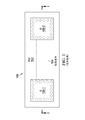
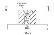
図3〜図6を参照すると、本発明に従った相互接続システム200−Aの例が示されている。この例示のシステム200−Aでは、回路アセンブリ206−A1及び206−A2が、PCB202−Aに固定された(即ち、接着された)誘電性導波路204−Aを介して互いに通信することができる。回路アセンブリ206−1及び206−2は、ボールグリッドアレイ(BGA)又ははんだボール(破線で示されている)を介してパッケージ基板304−A(例えば、PCBであり得る)に固定されたIC302−Aで形成され得る。パッケージ基板304−Aは、その後、BGA又ははんだボール(即ち、はんだボール301−A)を用いて、PCB202−Aに固定され得、それにより、IC302−Aが少なくとも1つのはんだボールに電気的に結合され得る。また、回路アセンブリ206−1及び206−2に付加的な機械的サポートを提供するように、パッケージ基板304−AとPCB202−Aとの間にアンダーフィル層303−Aも含まれ得る。パッケージ基板304−AとPCB202−Aは、例えば約0.25mm、離され得る。誘電性導波路システムの他の例は、同時継続中の2010年9月21日出願の米国特許出願番号12/887,270、発明の名称「高速デジタル相互接続及び方法」、及び同時継続中の2010年9月21日出願の米国特許出願番号12/887,323、発明の名称「サブミリメートル波通信リンクのためのチップと誘電性導波路間のインタフェース」に見出され得る。各同時継続中の出願は、あらゆる目的のための参照として本明細書に組み込まれる。
チップ間リンクを提供するために、パッケージ基板304−A及びPCB202−Aは、アンテナシステムを含む。この例(これは回路アセンブリ206−A1を示す)のためのアンテナシステムは、概して、マイクロストリップライン(パッケージ基板304−Aに統合された導電層)、接地平面306−A(パッケージ基板304−Aに統合された導電層)、及び接地平面308−A(パッケージ基板308−Aに統合された導電層)を含む。接地平面308−Aは、図示されるように及び例として、はんだボール301−Aを介して、接地平面306−Aに結合される(これにより、接地平面306−A及び308−Aが共に電気的に結合される)。この例で示すように、誘電性導波路204−Aは、回路アセンブリ206−A1及び206−A2と同じ側又は面に固定され、遷移領域314−Aの中に延びる。遷移領域314−Aは、コア310−Aの一部が、接地平面308−Aと、マイクロストリップライン208−A1の一部との間に位置するところである。典型的に、マイクロストリップライン208−A1(これは、パッケージ基板304−Aを介してIC302−Aに電気的に結合される)は、サブミリメートル(即ち、約0.5mm〜約1mm、又は約1mm未満の波長)又はテラヘルツ放射(即ち、約100GHz〜約1THz)を送信するように、寸法が定められる。この例の場合、RF又はワイヤレス信号を誘電性導波路204−Aに送信させるために、マイクロストリップライン208−A1は、遷移領域314−Aにおける境界により2つの部分を有する。マイクロストリップライン208−A1の1つの部分(これは、IC302−Aから遷移領域314−Aまで延びるように図示されている)は、接地平面306−A1に概して平行であり、そのため、電界がマイクロストリップライン208−A1とパッケージ基板304−A内の接地平面306−A1との間に延びる。マイクロストリップライン208−A1と接地平面306−A1との間の距離が相対的に短い(即ち、約0.2mm)ため、マイクロストリップライン208−A1のこの部分は、所望のインピーダンス(即ち、約50Ω)を達成するように狭くし得る。遷移領域では、マイクロストリップライン208−A1とその接地平面(接地平面308−A)との間の分離において、段階的増加(即ち、約0.25mm)がある。増加により、マイクロストリップライン208−A1のこの部分が、整合するインピーダンス(即ち、約50Ω)を有するようにより広くなる。これにより、RF信号が回路アセンブリ206−A1及び206−A2から直接的に伝播可能となる。遷移領域314−Aにおける境界が急であっても、IC302−A内で信号処理(即ち、事前歪み)を用いることによって、多くの問題(即ち、反射)が相殺又はフィルタされ得る。 In order to provide an inter-chip link, package substrate 304-A and PCB 202-A include an antenna system. The antenna system for this example (which shows circuit assembly 206-A1) is generally a microstrip line (a conductive layer integrated into package substrate 304-A), ground plane 306-A (package substrate 304-A). And a ground plane 308-A (conductive layer integrated with the package substrate 308-A). Ground plane 308-A is coupled to ground plane 306-A via solder balls 301-A, as shown and by way of example (so that ground planes 306-A and 308-A are both electrically connected). Combined). As shown in this example, dielectric waveguide 204-A is secured to the same side or face as circuit assemblies 206-A1 and 206-A2, and extends into transition region 314-A. Transition region 314-A is where a portion of core 310-A is located between ground plane 308-A and a portion of microstrip line 208-A1. Typically, microstrip line 208-A1 (which is electrically coupled to IC 302-A via package substrate 304-A) is sub-millimeter (ie, about 0.5 mm to about 1 mm, or about Dimensioned to transmit (less than 1 mm wavelength) or terahertz radiation (ie, about 100 GHz to about 1 THz). In this example, the microstrip line 208-A1 has two parts with a boundary in the transition region 314-A to transmit an RF or wireless signal to the dielectric waveguide 204-A. One portion of microstrip line 208-A1 (shown as extending from IC 302-A to transition region 314-A) is generally parallel to ground plane 306-A1, so that the electric field is microscopic. The strip line 208-A1 extends between the ground plane 306-A1 in the package substrate 304-A. Because the distance between microstrip line 208-A1 and ground plane 306-A1 is relatively short (ie, about 0.2 mm), this portion of microstrip line 208-A1 has a desired impedance (ie, about 50Ω) can be narrowed. In the transition region, there is a step increase (ie, about 0.25 mm) in the separation between the microstrip line 208-A1 and its ground plane (ground plane 308-A). With the increase, this portion of the microstrip line 208-A1 becomes wider to have a matching impedance (ie, about 50Ω). This allows RF signals to propagate directly from circuit assemblies 206-A1 and 206-A2. Many problems (ie, reflections) can be canceled or filtered by using signal processing (ie, predistortion) within IC 302-A, even if the boundaries in transition region 314-A are steep.
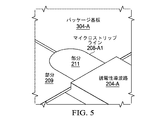
マイクロストリップライン208−A1は、他の形状も有し得る。図5には、マイクロストリップライン208−A1のための例示の構成が示されている。この構成では、マイクロストリップライン208−A1は、2つの部分209及び211を有する。図示されるように、部分209は、IC302−Aに電気的に結合されたフィードラインとして機能し得、部分211は、部分209の幅からより広くなる。この幅を広くすることは、テーパにより達成され得るが、図示されるように、部分209に電気的に結合された部分211の端部が丸くされている。
The microstrip line 208-A1 may have other shapes. FIG. 5 shows an exemplary configuration for the microstrip line 208-A1. In this configuration, the microstrip line 208-A1 has two
更に効率を改善するために、誘電性導波路204−A及びPCB202−Aが適切に構成され得る。典型的に及びこの例で示されるように、コア310−A(例えば、ポリアミド、ポリエステル、Rogers CorporationのRO3006(商標)又はRO3010(商標)で形成され得、例えば、約0.5mmの高さを有し得る)は、コア310−Aの残部を実質的に囲むクラッディング312−Aを用いて、PCB202−A(例えば、Rogers CorporationのRO3003(商標)で形成され得る)に固定される。クラッディング312−A及びPCB202−Aはいずれも、コア310−Aより低い誘電率を有し、クラッディング312−Aは、PCB202−Aと同じ又は同程度の誘電率を有し得る。これにより、電界がコア310−Aに閉じ込められる。また、誘電性導波路204−Aは、アンテナシステムから出された放射の波長(即ち、サブミリメートル波長)に適応するように寸法が定められ得る。 To further improve efficiency, dielectric waveguide 204-A and PCB 202-A can be appropriately configured. Typically and as shown in this example, core 310-A (eg, polyamide, polyester, Rogers Corporation's RO3006 ™ or RO3010 ™) may be formed, for example, having a height of about 0.5 mm. Is secured to PCB 202-A (eg, formed of Rogers Corporation's RO3003 ™) using a cladding 312-A that substantially surrounds the remainder of core 310-A. Both cladding 312 -A and PCB 202 -A have a lower dielectric constant than core 310 -A, and cladding 312 -A may have the same or similar dielectric constant as PCB 202 -A. Thereby, the electric field is confined in the core 310-A. In addition, the dielectric waveguide 204-A can be sized to accommodate the wavelength of radiation emitted from the antenna system (ie, a submillimeter wavelength).
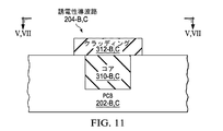
或いは、図7〜図12に示すように、誘電性導波路312−B、Cは、PCB202−B、Cに統合され得る。これらの例では、チャネルがPCB202−B、C、にルーティングされ得、誘電性導波路204−B、Cは、チャネル内のPCB202−B、Cに固定され得る。図示されるように及びコア310−Aと同様に、コア310−B、Cは、遷移領域314−B、Cの中に延びる。また、PCB202−B、Cは、図11の例に示されるように、クラッディング312−B、Cとしても用いられ得るが、代わりに、クラッディング材料がチャネルに含まれてもよい。また、PCB202−B、Cの上に延びる(破線で示される)クラッディング312−B、Cの部分は省かれ得る。チャネルに固定されたコア310−B、Cの端部も、テーパされ得(例えば、図8に示すように)、又は「矩形」に(例えば、図10に示すように)され得る。テーパされる場合、各段は、例えば、約5ミリメートル毎の深度で増分され得る。 Alternatively, as shown in FIGS. 7-12, dielectric waveguides 312 -B, C can be integrated into PCBs 202 -B, C. In these examples, the channel may be routed to PCBs 202-B, C, and dielectric waveguides 204-B, C may be fixed to PCBs 202-B, C in the channels. As shown and similar to core 310-A, cores 310-B, C extend into transition regions 314-B, C. PCBs 202-B, C can also be used as claddings 312-B, C, as shown in the example of FIG. 11, but alternatively, cladding material may be included in the channel. Also, the portion of the cladding 312-B, C (shown in broken lines) that extends above the PCBs 202-B, C can be omitted. The ends of the cores 310-B, C secured to the channel can also be tapered (eg, as shown in FIG. 8) or “rectangular” (eg, as shown in FIG. 10). If tapered, each step may be incremented, for example, at a depth of about every 5 millimeters.
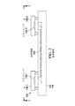
図7及び図8に、アンテナシステム及び遷移領域314−Bのための、1つの例示の構成(システム200−B)が示されている。回路アセンブリ206−B1(例えば)のためのアンテナシステムは概して、マイクロストリップライン208−B1(これは、パッケージ基板304−Bに位置し、IC302−Bに電気的に結合される)、及び接地平面306−B(これは、パッケージ基板304−B内に位置し、マイクロストリップライン208−B1の一部に概して平行であり、マイクロストリップライン208−B1の一部から離れている)で構成される。例えば、マイクロストリップライン208−B1の一部(これは、IC302−Bから遷移領域314−Bとの境界まで延びるように図示されている)と接地平面306−Bは、約0.2mm離され得る。接地平面308−B(これは、図示されるように及び例として、PCB202−Bに位置する)は、遷移領域314−B内のマイクロストリップライン208−B1の一部に平行であり、遷移領域314−B内のマイクロストリップライン208−B1の一部から離れている。マイクロストリップライン208−B1は、例えば、接地平面308−Bから約1mmの距離離され得る。この構成を有することによって、所望のインピーダンス(即ち、約50Ω)を提供するように、マイクロストリップライン208−B1の幅、及びマイクロストリップライン208−B1と接地平面308−Bとの間の距離、の寸法が定められ得る。典型的に、この例のためには、マイクロストリップライン208−B1の部分は、概して矩形であり、遷移領域における部分の幅が広い。例えば、これらの幅は、約50Ωの所望のインピーダンスを達成するための幅を有し得る。この例において示されるように、接地平面308−Bの1つの側から延びるバイア316があり、これにより、接地平面308−Bが(即ち、はんだボール301−Bを介して)接地平面306−Bに電気的に結合される。 FIGS. 7 and 8 illustrate one exemplary configuration (system 200-B) for the antenna system and transition region 314-B. The antenna system for circuit assembly 206-B1 (for example) is generally microstrip line 208-B1 (which is located on package substrate 304-B and electrically coupled to IC 302-B), and a ground plane. 306-B (which is located within the package substrate 304-B, is generally parallel to a portion of the microstrip line 208-B1, and is remote from a portion of the microstrip line 208-B1). . For example, a portion of the microstrip line 208-B1 (which is illustrated as extending from the IC 302-B to the boundary with the transition region 314-B) and the ground plane 306-B are separated by approximately 0.2 mm. obtain. The ground plane 308-B (which is located on the PCB 202-B as shown and by way of example) is parallel to a portion of the microstrip line 208-B1 in the transition region 314-B, and the transition region A portion of microstrip line 208-B1 in 314-B is remote. The microstrip line 208-B1 may be separated from the ground plane 308-B by a distance of about 1 mm, for example. By having this configuration, the width of the microstrip line 208-B1 and the distance between the microstrip line 208-B1 and the ground plane 308-B to provide the desired impedance (ie, approximately 50Ω), Dimensions can be defined. Typically, for this example, the portion of microstrip line 208-B1 is generally rectangular and the portion in the transition region is wide. For example, these widths may have a width to achieve a desired impedance of about 50Ω. As shown in this example, there is a via 316 extending from one side of ground plane 308-B so that ground plane 308-B (ie, via solder ball 301-B) is ground plane 306-B. Is electrically coupled.
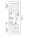
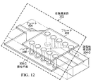
図9及び図10には、アンテナシステム及び遷移領域314−Cのための、他の例示の構成(システム200−C)が示されている。回路アセンブリ206−C1(例えば)のためのアンテナシステムは概して、マイクロストリップライン208−C1(これは、パッケージ基板304−Cに位置し、IC302−Bに電気的に結合される)、マイクロストリップライン320−1(これはPCB202−Cに位置する)、接地平面306−C(これは、パッケージ基板304−C内に位置し、マイクロストリップライン208−C1の一部に概して平行である)、及びバイア318(これは、パッケージ基板304−Cの1つの側とマイクロストリップライン208−C1との間に延び、これにより、マイクロストリップライン208−C1が、はんだボール301−C”を介して、マイクロストリップライン320−1に電気的に結合される)で構成される。例えば、マイクロストリップライン208−C1の一部(これは、IC302−Cから、遷移領域314−Cとの境界まで延びるように示されている)と接地平面306−Cは、約0.2mm離され得る。接地平面308−B(これは、図示されるように及び例として、PCB202−Bに位置する)は、遷移領域314−C内のマイクロストリップライン208−C1の一部に平行であり、遷移領域314−C内のマイクロストリップライン208−C1の一部から離れている。マイクロストリップライン208−B1は、例えば、接地平面308−Bから、約1mmの距離離され得る。この構成を有することにより、所望のインピーダンス(即ち、約50Ω)を提供するように、マイクロストリップライン208−C1の幅、及びマイクロストリップライン208−B1と接地平面306−Cとの間の距離、の寸法が定められ得る。典型的に、この例では、マイクロストリップライン208−C1の1つの部分(図ではIC302−Cから遷移領域314−Cまで延びるように示されている)は、所望のインピーダンス(即ち、約50Ω)を提供するように寸法が定められた幅(即ち、約25μm)を有し、もう別の部分(図では遷移領域314−Cの境界からパッケージ基板304−Cのエッジまで延びるように示されている)は、遷移がマイクロストリップライン320−1(これも、この放射を搬送するように寸法が定められる)と接地平面308−Bとの間の領域になるように定められる。典型的に、302−Cから遷移領域314−Cまで延びるように示されているマイクロストリップライン208−C1の一部は、一般的に、遷移領域314−Cの境界からパッケージ基板304−Cのエッジまで延びるように示されているマイクロストリップライン208−C1の部分より幅広い。この例に示すように、接地平面308−Bの1つの側から延びるバイア316が存在し、これにより、接地平面308−Cが、(即ち、はんだボール301−Cを介して)接地平面306−Cに電気的に結合され得る。 9 and 10 show another example configuration (system 200-C) for the antenna system and transition region 314-C. The antenna system for circuit assembly 206-C1 (for example) is generally microstrip line 208-C1 (which is located on package substrate 304-C and electrically coupled to IC 302-B), microstrip line. 320-1 (which is located on PCB 202-C), ground plane 306-C (which is located in package substrate 304-C and is generally parallel to a portion of microstrip line 208-C1), and Vias 318 (which extend between one side of the package substrate 304-C and the microstrip line 208-C1, so that the microstrip line 208-C1 is connected to the microstrip via the solder balls 301-C ″. For example, it is electrically coupled to the strip line 320-1. A portion of cross-trip line 208-C1 (which is shown extending from IC 302-C to the boundary with transition region 314-C) and ground plane 306-C may be separated by approximately 0.2 mm. The ground plane 308-B (which is located on the PCB 202-B as shown and as an example) is parallel to a portion of the microstrip line 208-C1 in the transition region 314-C and Separated from a portion of microstrip line 208-C1 in region 314-C, microstrip line 208-B1, for example, can be spaced a distance of about 1 mm from ground plane 308-B. The width of the microstrip line 208-C1 and the microstrip to provide the desired impedance (ie, about 50Ω) The distance between the line 208-B1 and the ground plane 306-C can be defined, typically in this example one portion of the microstrip line 208-C1 (from the IC 302-C in the figure to the transition region). Is shown to extend to 314-C) and has a width dimensioned to provide the desired impedance (ie, about 50Ω) (ie, about 25 μm) and another portion (see FIG. , The transition region 314-C is shown as extending from the boundary of the package substrate 304-C to the edge of the package substrate 304-C, and the transition is dimensioned so that the microstrip line 320-1 (also carries this radiation). ) And the ground plane 308-B, typically a microstrip shown as extending from 302-C to transition region 314-C. A portion of the p-line 208-C1 is generally wider than the portion of the microstrip line 208-C1 that is shown extending from the boundary of the transition region 314-C to the edge of the package substrate 304-C. As shown in this example, there is a via 316 extending from one side of the ground plane 308-B so that the ground plane 308-C is connected to the ground plane 306- (ie, via the solder balls 301-C). It can be electrically coupled to C.
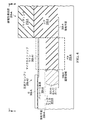
遷移領域314−Cの一部として、中に誘電性導波路204−Cのコア310−Cが延びる金属導波路322がある。金属導波路322の例が図12に示される。誘電性導波路204−Cとの所望の結合を達成するために(システム200−Bのいずれかのための)、金属導波路322が、プレート402及び404、接地平面308−C、及びバイア408で形成され得る。この例に示すように、プレート404(これは、例えば、銅で形成され得、マイクロストリップライン320−1に電気的に結合される)は、狭い部分及びテーパされた部分を含み、プレート406(これは、例えば、銅で形成され得る)に概して平行である。プレート404の狭い部分の幅は、所望のインピーダンスを達成するように(例えば、システム200−Cのアンテナシステムからのインピーダンスに整合させるように)選択される。また、プレート402は概して、プレート404と同一平面にあり得、プレート404に電気的に結合され得る。また、バイア408は、この例では、プレート402及び404と接地平面308−Cが共に電気的に結合されるようにプレート402と接地平面308−Cとの間に延びるように示されている。また、誘電性導波路204−Cが金属導波路322の中に延び得るように、バイア408は離間される。更に、誘電性導波路204−Cの端部の形状は、遷移領域314−Cの特性に影響を与え得、この例では、誘電性導波路の端部(これは、金属導波路322の中に延びる)はテーパされる。しかしながら、他の形状も可能である。
As part of the transition region 314-C is a
当業者であれば、本発明の請求の範囲内で、多くの変更が行なわれ得ること、また他の多くの実施形態が可能であることが理解されるであろう。 Those skilled in the art will appreciate that many modifications may be made and many other embodiments are possible within the scope of the claims of the present invention.
Claims (19)
回路ボード、
チャネル、
パッケージ基板、
集積回路(IC)、
金属導波路、及び
誘電体コア、
を含み、
前記回路ボードが、第1の側、第2の側、第1の接地平面、及び第1のマイクロストリップラインを有し、前記第1のマイクロストリップラインが前記第1の接地平面に概して平行であり、
前記チャネルが、前記回路ボードの前記第1の側に形成され、前記第1の接地平面が前記チャネルの少なくとも一部の下にあり、
前記パッケージ基板が、前記回路ボードの前記第1の側に固定され、
前記パッケージ基板が、
前記第1の接地平面に電気的に結合された第2の接地平面と、
前記第1及び第2の接地平面に実質的に平行である第2のマイクロストリップラインと、
を含み、
前記マイクロストリップラインが、第1の部分及び第2の部分を有し、
前記第1の部分が、前記第2の接地平面の少なくとも一部に重なり、且つ、前記第2の接地平面から第1の距離離れ、前記第2のマイクロストリップラインの前記第1の部分が、或る波長を有する放射を伝播するためのインピーダンスを有するように寸法が定められ、
前記第2の部分が、前記第1の接地平面の少なくとも一部に重なり、且つ、前記第1の接地平面から第2の距離離れ、前記第2の距離が前記第1の距離より大きく、前記第2のマイクロストリップラインの前記第2の部分が、前記波長を有する前記放射を伝播するための前記インピーダンスを有するように寸法が定められ、前記マイクロストリップラインの前記第2の部分が遷移領域内に位置し、前記第2のマイクロストリップラインの前記第2の部分が前記第1のマイクロストリップラインに電気的に結合され、
前記集積回路(IC)が、前記パッケージ基板に固定され、前記第2のマイクロストリップラインの前記第1の部分に電気的に結合され、
前記金属導波路が、前記チャネルに固定され、前記遷移領域に位置し、前記第1のマイクロストリップラインに電気的に結合され、
前記誘電体コアが、前記第1の接地平面の少なくとも一部に重なり、前記金属導波路の中に延び、前記チャネルに固定される、
装置。 A device,
Circuit board,
channel,
Package substrate,
Integrated circuit (IC),
A metal waveguide, and a dielectric core,
Including
The circuit board has a first side, a second side, a first ground plane, and a first microstrip line, wherein the first microstrip line is generally parallel to the first ground plane. Yes,
The channel is formed on the first side of the circuit board and the first ground plane is below at least a portion of the channel;
The package substrate is fixed to the first side of the circuit board;
The package substrate is
A second ground plane electrically coupled to the first ground plane;
A second microstrip line that is substantially parallel to the first and second ground planes;
Including
The microstrip line has a first portion and a second portion;
The first portion overlaps at least a portion of the second ground plane and is separated from the second ground plane by a first distance, and the first portion of the second microstrip line comprises: Dimensioned to have an impedance for propagating radiation having a wavelength,
The second portion overlaps at least a portion of the first ground plane and is separated from the first ground plane by a second distance, the second distance being greater than the first distance, The second portion of the second microstrip line is dimensioned to have the impedance for propagating the radiation having the wavelength, and the second portion of the microstrip line is within a transition region And the second portion of the second microstrip line is electrically coupled to the first microstrip line;
The integrated circuit (IC) is fixed to the package substrate and electrically coupled to the first portion of the second microstrip line;
The metal waveguide is fixed to the channel, located in the transition region, and electrically coupled to the first microstrip line;
The dielectric core overlaps at least a portion of the first ground plane, extends into the metal waveguide, and is secured to the channel;
apparatus.
前記第1のマイクロストリップラインと同一平面にあり、前記第1のマイクロストリップラインに電気的に結合された第1のプレート、
前記第1のプレートと同一平面にあり、前記第1のプレートに電気的に結合された第2のプレート、及び、
前記第2のプレートと前記第1の接地平面との間に延びる複数の導波路バイア、
を更に含む、装置。 7. The apparatus of claim 6, wherein the metal waveguide is
A first plate in the same plane as the first microstrip line and electrically coupled to the first microstrip line;
A second plate that is coplanar with the first plate and is electrically coupled to the first plate; and
A plurality of waveguide vias extending between the second plate and the first ground plane;
Further comprising an apparatus.
回路ボード、
チャネルネットワーク、
複数のパッケージ基板、
複数のIC、
複数の金属導波路、及び
誘電体コアネットワーク、
を含み、
前記回路ボードが、第1の側、第2の側、複数の回路ボード接地平面、及び複数の回路ボードマイクロストリップラインを有し、
前記チャネルネットワークが前記回路ボードの前記第1の側に形成され、各回路ボード接地平面が前記チャネルネットワークの少なくとも一部の下にあり、
前記複数のパッケージ基板の各パッケージ基板が前記回路ボードの前記第1の側に固定され、各々が、前記回路ボード接地平面の少なくとも1つ及び前記回路ボードマイクロストリップラインの少なくとも1つとコロケートされ(collocated)、各パッケージ基板が、パッケージ基板接地平面とパッケージ基板マイクロストリップラインとを含み、
前記パッケージ基板接地平面が、その回路ボード接地平面に電気的に結合され、
前記パッケージ基板マイクロストリップラインが、そのパッケージ基板接地平面及びその回路ボード接地平面に実質的に平行であり、
前記パッケージ基板マイクロストリップラインが、第1の部分及び第2の部分を有し、
前記第1の部分が、そのパッケージ基板接地平面の少なくとも一部に重なり、且つ、そのパッケージ基板接地平面から第1の距離離れ、前記パッケージ基板マイクロストリップラインの前記第1の部分が、或る波長を有する放射を伝播するためのインピーダンスを有するように寸法が定められ、
前記第2の部分が、その回路ボード接地平面の少なくとも一部に重なり、且つ、その回路ボード接地平面から第2の距離離れ、前記第2の距離が前記第1の距離より大きく、前記パッケージ基板マイクロストリップラインの前記第2の部分が、前記波長を有する前記放射を伝播するための前記インピーダンスを有するように寸法が定められ、前記パッケージ基板マイクロストリップラインの前記第2の部分が遷移領域内に位置し、
前記複数のICの各ICが、前記パッケージ基板の少なくとも1つに固定され、そのマイクロストリップラインの前記第1の部分に電気的に結合され、
前記複数の金属導波路の各金属導波路が、前記チャネルネットワークに固定され、前記パッケージ基板の少なくとも1つのための前記遷移領域に位置し、前記回路ボードマイクロストリップラインの少なくとも1つに電気的に結合され、
前記誘電体コアネットワークが、前記チャネルネットワークに固定され、且つ、複数の端部を有し、誘電導波路ネットワークからの各端部が、前記回路ボード接地平面の少なくとも1つのの少なくとも一部に重なり、その金属導波路内に延びる、
装置。 A device,
Circuit board,
Channel network,
Multiple package substrates,
Multiple ICs,
A plurality of metal waveguides, and a dielectric core network,
Including
The circuit board has a first side, a second side, a plurality of circuit board ground planes, and a plurality of circuit board microstrip lines;
The channel network is formed on the first side of the circuit board, and each circuit board ground plane is below at least a portion of the channel network;
Each package substrate of the plurality of package substrates is secured to the first side of the circuit board, each collocated with at least one of the circuit board ground plane and at least one of the circuit board microstrip lines. ), Each package substrate includes a package substrate ground plane and a package substrate microstrip line;
The package substrate ground plane is electrically coupled to the circuit board ground plane;
The package substrate microstrip line is substantially parallel to the package substrate ground plane and the circuit board ground plane;
The package substrate microstrip line has a first portion and a second portion;
The first portion overlaps at least a portion of the package substrate ground plane and is separated from the package substrate ground plane by a first distance, and the first portion of the package substrate microstrip line has a wavelength Dimensioned to have an impedance for propagating radiation having
The second portion overlaps at least a portion of the circuit board ground plane, is separated from the circuit board ground plane by a second distance, and the second distance is greater than the first distance; The second portion of the microstrip line is dimensioned to have the impedance for propagating the radiation having the wavelength, and the second portion of the package substrate microstrip line is within a transition region. Position to,
Each of the plurality of ICs is fixed to at least one of the package substrates and electrically coupled to the first portion of the microstrip line;
Each metal waveguide of the plurality of metal waveguides is secured to the channel network, is located in the transition region for at least one of the package substrates, and is electrically connected to at least one of the circuit board microstrip lines. Combined,
The dielectric core network is fixed to the channel network and has a plurality of ends, each end from the dielectric waveguide network overlapping at least a portion of at least one of the circuit board ground planes. Extending into the metal waveguide,
apparatus.
第1のプレートであって、その回路ボードマイクロストリップラインと同一平面にあり、その回路ボードマイクロストリップラインに電気的に結合された前記第1のプレート、
第2のプレートであって、前記第1のプレートと同一平面にあり、前記第1のプレートに電気的に結合された、前記第2のプレート、及び
複数の導波路バイアであって、前記第2のプレートとその回路ボード接地平面との間に延びる前記複数の導波路バイア、
を更に含む装置。 14. The apparatus of claim 13, wherein each metal waveguide is
A first plate, said first plate being coplanar with the circuit board microstrip line and electrically coupled to the circuit board microstrip line;
A second plate, wherein the second plate is coplanar with the first plate and is electrically coupled to the first plate; and a plurality of waveguide vias, The plurality of waveguide vias extending between the two plates and the circuit board ground plane;
Further comprising a device.
回路ボード、
チャネル、
第1のパッケージ基板、
第1のIC、
第2のパッケージ基板、
第2のIC、
第1の金属導波路、
第2の金属導波路、及び
誘電体コア、
を含み、
前記回路ボードが、第1の側、第2の側、第1の接地平面、第2の接地平面、第1のマイクロストリップライン、及び第2のマイクロストリップラインを有し、前記第1及び第2のマイクロストリップラインが前記回路ボードの前記第1の側に形成され、前記第1のマイクロストリップラインが、前記第1の接地平面とコロケートされ、前記第1の接地平面に概して平行であり、前記第2のマイクロストリップラインが、前記第2の接地平面とコロケートされ、前記第2の接地平面に概して平行であり、
前記チャネルが、前記回路ボードの前記第1の側に形成され、第1の端部及び第2の端部を有し、前記チャネルの前記第1の端部が前記第1の接地平面の少なくとも一部に重なり、前記チャネルの前記第2の端部が前記第2の接地平面の少なくとも一部に重なり、
前記第1のパッケージ基板が前記回路ボードの前記第1の側に固定され、前記第1のパッケージ基板が、第3の接地平面及び第3のマイクロストリップラインを含み、
前記第3の接地平面が前記第1の接地平面に電気的に結合され、
前記第3のマイクロストリップラインが前記第1及び第3の接地平面に実質的に平行であり、
前記第3のマイクロストリップラインが第1の部分及び第2の部分を有し、
前記第1の部分が、前記第3の接地平面の少なくとも一部に重なり、且つ、前記第3の接地平面から第1の距離離れ、前記第3のマイクロストリップラインの前記第1の部分が、或る波長を有する放射を伝播するためのインピーダンスを有するように寸法が定められ、
前記第2の部分が、前記第1の接地平面の少なくとも一部に重なり、且つ、前記第1の接地平面から第2の距離離れ、前記第2の距離が前記第1の距離より大きく、前記第3のマイクロストリップラインの前記第2の部分が、前記波長を有する前記放射を伝播するための前記インピーダンスを有するように寸法が定められ、前記第3のマイクロストリップラインの前記第2の部分が第1の遷移領域内に位置し、
前記第1のICが、前記パッケージ基板に固定され、前記第3のマイクロストリップラインの前記第1の部分に電気的に結合され、
前記第2のパッケージ基板が前記回路ボードの前記第1の側に固定され、前記第2のパッケージ基板が、第4の接地平面及び第4のマイクロストリップラインを含み、
前記第4の接地平面が前記第2の接地平面に電気的に結合され、
前記第4のマイクロストリップラインが、前記第2及び第4の接地平面に実質的に平行であり、
前記第4のマイクロストリップラインが第1の部分及び第2の部分を有し、
前記第4のマイクロストリップラインの前記第1の部分が、前記第4の接地平面の少なくとも一部に重なり、且つ、前記第4の接地平面から第3の距離離れ、前記第4のマイクロストリップラインの前記第1の部分が、前記波長を有する前記放射を伝播するための前記インピーダンスを有するように寸法が定められ、
前記第4のマイクロストリップラインの前記第2の部分が、前記第2の接地平面の少なくとも一部に重なり、且つ、前記第2の接地平面から第4の距離離れ、前記第4の距離が前記第3の距離より大きく、前記第4のマイクロストリップラインの前記第2の部分が、前記波長を有する前記放射を伝播するための前記インピーダンスを有するように寸法が定められ、前記第2のマイクロストリップラインの前記第2の部分が第2の遷移領域内に位置し、
前記第2のICが、前記パッケージ基板に固定され、前記第4のマイクロストリップラインの前記第1の部分に電気的に結合され、
前記第1の金属導波路が、前記チャネルに固定され、前記第1の遷移領域に位置し、前記第1のマイクロストリップラインに電気的に結合され、
前記第2の金属導波路が、前記チャネルに固定され、前記第2の遷移領域内に位置し、前記第2のマイクロストリップラインに電気的に結合され、
前記誘電体コアが、第1及び第2の端部を備え、前記誘電体コアが前記チャネルに固定され、前記誘電体コアの前記第1の端部が前記第1の接地平面の少なくとも一部に重なり、前記誘電体コアの前記第2の端部が前記第2の接地平面の少なくとも一部に重なり、前記誘電体コアの前記第1の端部が前記第1の金属導波路の中に延び、前記誘電体コアの前記第2の端部が前記第2の金属導波路の中に延び、前記誘電体コアが、前記回路ボードの前記誘電率より大きい誘電率を有する、
装置。 A device,
Circuit board,
channel,
A first package substrate;
The first IC,
A second package substrate,
The second IC,
A first metal waveguide,
A second metal waveguide, and a dielectric core,
Including
The circuit board includes a first side, a second side, a first ground plane, a second ground plane, a first microstrip line, and a second microstrip line, the first and second Two microstrip lines are formed on the first side of the circuit board, the first microstrip line is collocated with the first ground plane and generally parallel to the first ground plane; The second microstrip line is collocated with the second ground plane and is generally parallel to the second ground plane;
The channel is formed on the first side of the circuit board and has a first end and a second end, and the first end of the channel is at least of the first ground plane. Overlapping the portion, the second end of the channel overlaps at least a portion of the second ground plane,
The first package substrate is fixed to the first side of the circuit board, and the first package substrate includes a third ground plane and a third microstrip line;
The third ground plane is electrically coupled to the first ground plane;
The third microstrip line is substantially parallel to the first and third ground planes;
The third microstrip line has a first portion and a second portion;
The first portion overlaps at least a portion of the third ground plane and is separated from the third ground plane by a first distance, and the first portion of the third microstrip line includes: Dimensioned to have an impedance for propagating radiation having a wavelength,
The second portion overlaps at least a portion of the first ground plane and is separated from the first ground plane by a second distance, the second distance being greater than the first distance, The second portion of the third microstrip line is dimensioned to have the impedance for propagating the radiation having the wavelength, and the second portion of the third microstrip line is Located in the first transition region,
The first IC is fixed to the package substrate and electrically coupled to the first portion of the third microstrip line;
The second package substrate is secured to the first side of the circuit board, and the second package substrate includes a fourth ground plane and a fourth microstrip line;
The fourth ground plane is electrically coupled to the second ground plane;
The fourth microstrip line is substantially parallel to the second and fourth ground planes;
The fourth microstrip line has a first portion and a second portion;
The first portion of the fourth microstrip line overlaps at least a portion of the fourth ground plane and is separated from the fourth ground plane by a third distance, the fourth microstrip line; The first portion of is dimensioned to have the impedance for propagating the radiation having the wavelength;
The second portion of the fourth microstrip line overlaps at least a portion of the second ground plane and is a fourth distance away from the second ground plane, the fourth distance being the The second microstrip is dimensioned such that the second portion of the fourth microstrip line is greater than a third distance and has the impedance for propagating the radiation having the wavelength. The second portion of the line is located within the second transition region;
The second IC is fixed to the package substrate and electrically coupled to the first portion of the fourth microstrip line;
The first metal waveguide is fixed to the channel, located in the first transition region, and electrically coupled to the first microstrip line;
The second metal waveguide is fixed to the channel, is located in the second transition region, and is electrically coupled to the second microstrip line;
The dielectric core includes first and second ends, the dielectric core is fixed to the channel, and the first end of the dielectric core is at least part of the first ground plane. And the second end of the dielectric core overlaps at least a portion of the second ground plane, and the first end of the dielectric core is in the first metal waveguide. Extending, the second end of the dielectric core extends into the second metal waveguide, and the dielectric core has a dielectric constant greater than the dielectric constant of the circuit board;
apparatus.
第1のプレートであって、そのマイクロストリップラインと同一平面にあり、そのマイクロストリップラインに電気的に結合された前記第1のプレート、
前記第1のプレートと同一平面にあり、前記第1のプレートに電気的に結合された第2のプレート、及び
前記第2のプレートとその回路ボード接地平面との間に延びる複数の導波路バイア、
を更に含む装置。 19. The apparatus of claim 18, wherein each of the first and second metal waveguides is
A first plate that is coplanar with the microstrip line and is electrically coupled to the microstrip line;
A second plate that is coplanar with the first plate and electrically coupled to the first plate; and a plurality of waveguide vias extending between the second plate and its circuit board ground plane ,
Further comprising a device.
Applications Claiming Priority (3)
| Application Number | Priority Date | Filing Date | Title |
|---|---|---|---|
| US13/439,646 | 2012-04-04 | ||
| US13/439,646 US20130265734A1 (en) | 2012-04-04 | 2012-04-04 | Interchip communication using embedded dielectric and metal waveguides |
| PCT/US2013/035322 WO2013152226A1 (en) | 2012-04-04 | 2013-04-04 | Interchip communication using embedded dielectric and metal waveguides |
Publications (1)
| Publication Number | Publication Date |
|---|---|
| JP2015515213A true JP2015515213A (en) | 2015-05-21 |
Family
ID=49292154
Family Applications (1)
| Application Number | Title | Priority Date | Filing Date |
|---|---|---|---|
| JP2015504734A Pending JP2015515213A (en) | 2012-04-04 | 2013-04-04 | Chip-to-chip communication using buried dielectric and metal waveguides |
Country Status (4)
| Country | Link |
|---|---|
| US (1) | US20130265734A1 (en) |
| JP (1) | JP2015515213A (en) |
| CN (1) | CN104220910B (en) |
| WO (1) | WO2013152226A1 (en) |
Cited By (1)
| Publication number | Priority date | Publication date | Assignee | Title |
|---|---|---|---|---|
| US10199335B2 (en) | 2016-03-10 | 2019-02-05 | Fujitsu Limited | Electronic device including coupling structure along with waveguide, and electronic equipment |
Families Citing this family (16)
| Publication number | Priority date | Publication date | Assignee | Title |
|---|---|---|---|---|
| US20130265733A1 (en) * | 2012-04-04 | 2013-10-10 | Texas Instruments Incorporated | Interchip communication using an embedded dielectric waveguide |
| US9405064B2 (en) * | 2012-04-04 | 2016-08-02 | Texas Instruments Incorporated | Microstrip line of different widths, ground planes of different distances |
| US9601819B2 (en) * | 2013-02-27 | 2017-03-21 | Texas Instruments Incorporated | Dielectric waveguide with extending connector and affixed deformable material |
| US9112253B2 (en) * | 2013-03-19 | 2015-08-18 | Texas Instruments Incorporated | Dielectric waveguide combined with electrical cable |
| US9515368B2 (en) * | 2014-03-11 | 2016-12-06 | Nxp B.V. | Transmission line interconnect |
| US9715131B2 (en) | 2014-09-11 | 2017-07-25 | Taiwan Semiconductor Manufacturing Co., Ltd. | Integrated fan-out package including dielectric waveguide |
| CN104836619B (en) | 2015-03-30 | 2017-08-29 | 青岛海信宽带多媒体技术有限公司 | A kind of optical device |
| CN108063362A (en) | 2015-03-30 | 2018-05-22 | 青岛海信宽带多媒体技术有限公司 | A kind of laser |
| US10319689B2 (en) * | 2015-12-01 | 2019-06-11 | Nxp Usa, Inc. | Antenna assembly for wafer level packaging |
| DE102016102109A1 (en) * | 2016-01-29 | 2017-08-03 | Taiwan Semiconductor Manufacturing Company, Ltd. | INTEGRATED FAN-OUT HOUSING WITH DIELECTRIC WAVE GUIDE |
| US11211345B2 (en) | 2017-06-19 | 2021-12-28 | Intel Corporation | In-package RF waveguides as high bandwidth chip-to-chip interconnects and methods for using the same |
| KR102678311B1 (en) * | 2018-08-30 | 2024-06-25 | 삼성전자주식회사 | electronic device including semiconductor package having package ball |
| DE102019101276A1 (en) * | 2019-01-18 | 2020-07-23 | Rosenberger Hochfrequenztechnik Gmbh & Co. Kg | Waveguide arrangement, waveguide transition and use of a waveguide arrangement |
| US11581272B2 (en) * | 2019-03-22 | 2023-02-14 | Intel Corporation | Contactless high-frequency interconnect |
| CN113078431B (en) * | 2021-03-26 | 2022-03-15 | 电子科技大学 | Broadband high-flatness terahertz chip-to-chip interconnection structure |
| CN115308850B (en) * | 2021-05-08 | 2024-10-15 | 鹏鼎控股(深圳)股份有限公司 | Photoelectric composite circuit board and manufacturing method thereof |
Family Cites Families (17)
| Publication number | Priority date | Publication date | Assignee | Title |
|---|---|---|---|---|
| US3932823A (en) * | 1975-04-23 | 1976-01-13 | The United States Of America As Represented By The Secretary Of The Navy | Microstrip to waveguide adapter |
| WO1994006052A1 (en) * | 1992-09-10 | 1994-03-17 | Fujitsu Limited | Optical circuit system and its constituents |
| JPH09289404A (en) * | 1996-04-24 | 1997-11-04 | Honda Motor Co Ltd | Ribbon, bonding wire and microwave circuit package |
| US6175287B1 (en) * | 1997-05-28 | 2001-01-16 | Raytheon Company | Direct backside interconnect for multiple chip assemblies |
| JP3209183B2 (en) * | 1998-07-08 | 2001-09-17 | 日本電気株式会社 | High frequency signal integrated circuit package and method of manufacturing the same |
| JP4540275B2 (en) * | 2000-12-22 | 2010-09-08 | イビデン株式会社 | IC chip mounting substrate and manufacturing method of IC chip mounting substrate |
| US20030057544A1 (en) * | 2001-09-13 | 2003-03-27 | Nathan Richard J. | Integrated assembly protocol |
| US6646526B2 (en) * | 2002-03-14 | 2003-11-11 | M/A-Com, Inc. | Surface mountable microwave filter configuration and method of fabricating same |
| JP2004153367A (en) * | 2002-10-29 | 2004-05-27 | Tdk Corp | High frequency module, and mode converting structure and method |
| US7327022B2 (en) * | 2002-12-30 | 2008-02-05 | General Electric Company | Assembly, contact and coupling interconnection for optoelectronics |
| US7276988B2 (en) * | 2004-06-30 | 2007-10-02 | Endwave Corporation | Multi-substrate microstrip to waveguide transition |
| US8706050B2 (en) * | 2008-07-31 | 2014-04-22 | Kyocera Corporation | Matching circuit, wiring board, and transmitter, receiver, transceiver, and radar apparatus that have the matching circuit |
| KR101225038B1 (en) * | 2009-06-16 | 2013-01-23 | 전북대학교산학협력단 | Tag antenna using microstrip lines and manufacturing method thereof, RFID tag |
| US8019187B1 (en) * | 2009-08-17 | 2011-09-13 | Banpil Photonics, Inc. | Super high-speed chip to chip interconnects |
| JP5412372B2 (en) * | 2010-04-30 | 2014-02-12 | 株式会社フジクラ | Semiconductor mounting equipment |
| US20130265733A1 (en) * | 2012-04-04 | 2013-10-10 | Texas Instruments Incorporated | Interchip communication using an embedded dielectric waveguide |
| US9405064B2 (en) * | 2012-04-04 | 2016-08-02 | Texas Instruments Incorporated | Microstrip line of different widths, ground planes of different distances |
-
2012
- 2012-04-04 US US13/439,646 patent/US20130265734A1/en not_active Abandoned
-
2013
- 2013-04-04 JP JP2015504734A patent/JP2015515213A/en active Pending
- 2013-04-04 CN CN201380018528.5A patent/CN104220910B/en active Active
- 2013-04-04 WO PCT/US2013/035322 patent/WO2013152226A1/en not_active Ceased
Cited By (1)
| Publication number | Priority date | Publication date | Assignee | Title |
|---|---|---|---|---|
| US10199335B2 (en) | 2016-03-10 | 2019-02-05 | Fujitsu Limited | Electronic device including coupling structure along with waveguide, and electronic equipment |
Also Published As
| Publication number | Publication date |
|---|---|
| CN104220910A (en) | 2014-12-17 |
| CN104220910B (en) | 2017-11-28 |
| US20130265734A1 (en) | 2013-10-10 |
| WO2013152226A1 (en) | 2013-10-10 |
Similar Documents
| Publication | Publication Date | Title |
|---|---|---|
| JP6427626B2 (en) | Inter-chip communication using dielectric waveguides | |
| CN104204878B (en) | Device for communicating between integrated circuits via dielectric waveguides | |
| JP2015515213A (en) | Chip-to-chip communication using buried dielectric and metal waveguides | |
| JP5580994B2 (en) | Optical module | |
| KR101512816B1 (en) | Flexible printed circuit board and optical communication module comprising the same | |
| US8989531B2 (en) | Optical-electrical wiring board and optical module | |
| US10103418B2 (en) | First EM-tunnel embedded in a first PCB and free space coupled to a second EM-tunnel embedded in a second PCB | |
| CN111308620B (en) | Optical module | |
| US10879575B2 (en) | Embedded filtering in PCB integrated ultra high speed dielectric waveguides using photonic band gap structures | |
| US10622695B2 (en) | Multi-width waveguide including first and second waveguide regions of differing widths and heights for providing impedance matching to an integrated circuit | |
| US8861917B2 (en) | Opto-electric circuit board including metal-slotted optical waveguide and opto-electric simultaneous communication system | |
| CN115236808B (en) | Circuit board and optical module | |
| CN111954954A (en) | Connectors for connecting waveguides and substrates | |
| JP2007207803A (en) | Optical transmitting module | |
| JP7769265B2 (en) | Optical Module | |
| JP5855956B2 (en) | Optical wiring board and optical wiring module | |
| Kim et al. | 12-Channel optical transmitter on an organic substrate for optical interconnections |