JP2015217543A - Recording head - Google Patents
Recording head Download PDFInfo
- Publication number
- JP2015217543A JP2015217543A JP2014100913A JP2014100913A JP2015217543A JP 2015217543 A JP2015217543 A JP 2015217543A JP 2014100913 A JP2014100913 A JP 2014100913A JP 2014100913 A JP2014100913 A JP 2014100913A JP 2015217543 A JP2015217543 A JP 2015217543A
- Authority
- JP
- Japan
- Prior art keywords
- substrate
- recording head
- supply port
- organic material
- head according
- Prior art date
- Legal status (The legal status is an assumption and is not a legal conclusion. Google has not performed a legal analysis and makes no representation as to the accuracy of the status listed.)
- Granted
Links
Images
Classifications
-
- B—PERFORMING OPERATIONS; TRANSPORTING
- B41—PRINTING; LINING MACHINES; TYPEWRITERS; STAMPS
- B41J—TYPEWRITERS; SELECTIVE PRINTING MECHANISMS, i.e. MECHANISMS PRINTING OTHERWISE THAN FROM A FORME; CORRECTION OF TYPOGRAPHICAL ERRORS
- B41J2/00—Typewriters or selective printing mechanisms characterised by the printing or marking process for which they are designed
- B41J2/005—Typewriters or selective printing mechanisms characterised by the printing or marking process for which they are designed characterised by bringing liquid or particles selectively into contact with a printing material
- B41J2/01—Ink jet
- B41J2/135—Nozzles
- B41J2/14—Structure thereof only for on-demand ink jet heads
- B41J2/1433—Structure of nozzle plates
-
- B—PERFORMING OPERATIONS; TRANSPORTING
- B41—PRINTING; LINING MACHINES; TYPEWRITERS; STAMPS
- B41J—TYPEWRITERS; SELECTIVE PRINTING MECHANISMS, i.e. MECHANISMS PRINTING OTHERWISE THAN FROM A FORME; CORRECTION OF TYPOGRAPHICAL ERRORS
- B41J2/00—Typewriters or selective printing mechanisms characterised by the printing or marking process for which they are designed
- B41J2/005—Typewriters or selective printing mechanisms characterised by the printing or marking process for which they are designed characterised by bringing liquid or particles selectively into contact with a printing material
- B41J2/01—Ink jet
- B41J2/135—Nozzles
- B41J2/14—Structure thereof only for on-demand ink jet heads
- B41J2/14016—Structure of bubble jet print heads
- B41J2/14024—Assembling head parts
-
- B—PERFORMING OPERATIONS; TRANSPORTING
- B41—PRINTING; LINING MACHINES; TYPEWRITERS; STAMPS
- B41J—TYPEWRITERS; SELECTIVE PRINTING MECHANISMS, i.e. MECHANISMS PRINTING OTHERWISE THAN FROM A FORME; CORRECTION OF TYPOGRAPHICAL ERRORS
- B41J2/00—Typewriters or selective printing mechanisms characterised by the printing or marking process for which they are designed
- B41J2/005—Typewriters or selective printing mechanisms characterised by the printing or marking process for which they are designed characterised by bringing liquid or particles selectively into contact with a printing material
- B41J2/01—Ink jet
- B41J2/135—Nozzles
- B41J2/14—Structure thereof only for on-demand ink jet heads
- B41J2/14016—Structure of bubble jet print heads
- B41J2/14145—Structure of the manifold
-
- B—PERFORMING OPERATIONS; TRANSPORTING
- B41—PRINTING; LINING MACHINES; TYPEWRITERS; STAMPS
- B41J—TYPEWRITERS; SELECTIVE PRINTING MECHANISMS, i.e. MECHANISMS PRINTING OTHERWISE THAN FROM A FORME; CORRECTION OF TYPOGRAPHICAL ERRORS
- B41J2/00—Typewriters or selective printing mechanisms characterised by the printing or marking process for which they are designed
- B41J2/005—Typewriters or selective printing mechanisms characterised by the printing or marking process for which they are designed characterised by bringing liquid or particles selectively into contact with a printing material
- B41J2/01—Ink jet
- B41J2/135—Nozzles
- B41J2/16—Production of nozzles
- B41J2/162—Manufacturing of the nozzle plates
-
- B—PERFORMING OPERATIONS; TRANSPORTING
- B41—PRINTING; LINING MACHINES; TYPEWRITERS; STAMPS
- B41J—TYPEWRITERS; SELECTIVE PRINTING MECHANISMS, i.e. MECHANISMS PRINTING OTHERWISE THAN FROM A FORME; CORRECTION OF TYPOGRAPHICAL ERRORS
- B41J2/00—Typewriters or selective printing mechanisms characterised by the printing or marking process for which they are designed
- B41J2/005—Typewriters or selective printing mechanisms characterised by the printing or marking process for which they are designed characterised by bringing liquid or particles selectively into contact with a printing material
- B41J2/01—Ink jet
- B41J2/135—Nozzles
- B41J2/16—Production of nozzles
- B41J2/1621—Manufacturing processes
- B41J2/1623—Manufacturing processes bonding and adhesion
-
- B—PERFORMING OPERATIONS; TRANSPORTING
- B41—PRINTING; LINING MACHINES; TYPEWRITERS; STAMPS
- B41J—TYPEWRITERS; SELECTIVE PRINTING MECHANISMS, i.e. MECHANISMS PRINTING OTHERWISE THAN FROM A FORME; CORRECTION OF TYPOGRAPHICAL ERRORS
- B41J2202/00—Embodiments of or processes related to ink-jet or thermal heads
- B41J2202/01—Embodiments of or processes related to ink-jet heads
- B41J2202/11—Embodiments of or processes related to ink-jet heads characterised by specific geometrical characteristics
-
- Y—GENERAL TAGGING OF NEW TECHNOLOGICAL DEVELOPMENTS; GENERAL TAGGING OF CROSS-SECTIONAL TECHNOLOGIES SPANNING OVER SEVERAL SECTIONS OF THE IPC; TECHNICAL SUBJECTS COVERED BY FORMER USPC CROSS-REFERENCE ART COLLECTIONS [XRACs] AND DIGESTS
- Y10—TECHNICAL SUBJECTS COVERED BY FORMER USPC
- Y10T—TECHNICAL SUBJECTS COVERED BY FORMER US CLASSIFICATION
- Y10T156/00—Adhesive bonding and miscellaneous chemical manufacture
- Y10T156/10—Methods of surface bonding and/or assembly therefor
Landscapes
- Engineering & Computer Science (AREA)
- Manufacturing & Machinery (AREA)
- Particle Formation And Scattering Control In Inkjet Printers (AREA)
Abstract
【課題】 基板の変形を簡易な方法で抑制した記録ヘッドを提供すること。【解決手段】 基板と、流路を形成する流路形成部材とを有する記録ヘッドであって、前記基板には基板を貫通する供給口が形成されており、前記流路と前記供給口とは連通しており、前記供給口の内部に、前記供給口を形成し前記供給口を挟んで対向する2つの面をつなぐ、有機材料で形成された部材が形成されていることを特徴とする記録ヘッド。【選択図】 図5To provide a recording head in which deformation of a substrate is suppressed by a simple method. A recording head having a substrate and a flow path forming member for forming a flow path, wherein a supply port that penetrates the substrate is formed in the substrate, and the flow path and the supply port are defined as follows. A member made of an organic material is formed, which is in communication, and is formed inside the supply port and connects the two surfaces that are opposed to each other with the supply port interposed therebetween. head. [Selection] Figure 5
Description
本発明は、供給口が形成された基板を有する記録ヘッドに関する。 The present invention relates to a recording head having a substrate on which a supply port is formed.
インクジェットプリンタに代表される記録装置は、記録ヘッドを有する。記録ヘッドは、液体等を吐出する部分であり、基板と、流路を形成する流路形成部材とを有する。基板には、基板を貫通する供給口が形成されている。 A recording apparatus typified by an ink jet printer has a recording head. The recording head is a part that discharges liquid or the like, and includes a substrate and a flow path forming member that forms a flow path. A supply port that penetrates the substrate is formed in the substrate.
従来、このような記録ヘッドには、基板の変形という課題があった。例えば、基板の周囲が封止材で封止されている場合には、封止材が収縮することによって基板が変形することがある。基板の変形は、このような封止材によるものに限らず、周囲の様々な環境変化によって起こる。特に、基板が長尺化するにつれて、基板の変形は発生しやすくなる傾向にあった。基板が変形すると、基板上に流路形成部材が形成されていた場合には流路形成部材が変形したり、流路形成部材が基板から剥がれたりする場合がある。その結果、流路が変形することになるので、記録精度が低くなる場合がある。 Conventionally, such a recording head has a problem of deformation of the substrate. For example, when the periphery of the substrate is sealed with a sealing material, the substrate may be deformed by contraction of the sealing material. The deformation of the substrate is not limited to such a sealing material, but is caused by various environmental changes in the surroundings. In particular, as the substrate becomes longer, the substrate tends to be easily deformed. When the substrate is deformed, if the flow path forming member is formed on the substrate, the flow path forming member may be deformed or the flow path forming member may be peeled off from the substrate. As a result, since the flow path is deformed, the recording accuracy may be lowered.
このような課題を解決する方法として、基板の大きさを大きくすることで、基板の剛性を増すことが考えられる。 As a method for solving such a problem, it is conceivable to increase the rigidity of the substrate by increasing the size of the substrate.
また、他の解決方法として、特許文献1には、基板の供給口の内部に、基板の一部であるシリコンで形成された梁構造を設けることが記載されている。 As another solution, Patent Document 1 describes that a beam structure formed of silicon which is a part of a substrate is provided inside a substrate supply port.
上述のように、基板を大きくしていくと、基板の剛性は向上する。しかし、その分だけコストが高くなる。基板は、ウエハ上に流路形成部材等を形成し、これをダイシング等により切り出すことで製造される。即ち、基板が大きくなるにつれて、1枚のウエハから切り出せる基板の数が少なくなる。 As described above, as the substrate is enlarged, the rigidity of the substrate is improved. However, the cost increases accordingly. The substrate is manufactured by forming a flow path forming member or the like on the wafer and cutting it out by dicing or the like. That is, as the substrate becomes larger, the number of substrates that can be cut out from one wafer decreases.
一方、特許文献1に記載の、供給口の内部にシリコンで形成される梁構造を形成する方法は、基板の大きさを変えなくても剛性を向上させることができる。但し、吐出口や供給口を形成するのと同時に基板の一部を梁構造として残すので、その製造プロセスは複雑であり、やはりコストが高くなる傾向にある。 On the other hand, the method of forming a beam structure formed of silicon inside the supply port described in Patent Document 1 can improve rigidity without changing the size of the substrate. However, since a part of the substrate is left as a beam structure at the same time when the discharge port and the supply port are formed, the manufacturing process is complicated and the cost tends to increase.
本発明は、このような課題を鑑み、基板の変形を簡易な方法で抑制した記録ヘッドを提供することを目的とする。 The present invention has been made in view of the above problems, and an object of the present invention is to provide a recording head in which deformation of a substrate is suppressed by a simple method.
上記課題は、以下の本発明によって解決される。即ち本発明は、基板と、流路を形成する流路形成部材とを有する記録ヘッドであって、前記基板には基板を貫通する供給口が形成されており、前記流路と前記供給口とは連通しており、前記供給口の内部に、前記供給口を形成し前記供給口を挟んで対向する2つの面をつなぐ、有機材料で形成された部材が形成されていることを特徴とする記録ヘッドである。 The above problems are solved by the present invention described below. That is, the present invention is a recording head having a substrate and a flow path forming member that forms a flow path, wherein the substrate has a supply port penetrating the substrate, and the flow path, the supply port, Are connected to each other, and a member made of an organic material is formed in the supply port to form the supply port and connect two surfaces facing each other with the supply port interposed therebetween. It is a recording head.
本発明によれば、基板の変形を簡易な方法で抑制した記録ヘッドを提供することができる。 According to the present invention, it is possible to provide a recording head in which deformation of a substrate is suppressed by a simple method.
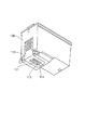
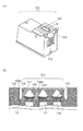
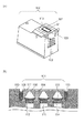
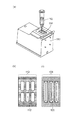
図1は、本発明の記録ヘッド100の構成を示す斜視図である。記録ヘッド100に搭載されるチップ101は電気配線テープ102に接合されており、電気配線テープ102を介してキャリッジと電気的に接触することで、圧力発生素子106へ電気信号が送られて記録動作が行われる。チップ101の電気配線テープ102の電気接合部は、封止材103により被覆保護されている。
FIG. 1 is a perspective view showing a configuration of a
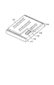
図2は、本発明の記録ヘッド100が有するチップ101の模式図である。チップ101は、基板104と流路形成部材105で構成される。流路形成部材105は、記録材料の流路を形成する。記録材料としては、インク等が挙げられる。以下、記録材料としてインクを用いた例で説明する。流路形成部材105は、樹脂や無機材料で形成される。樹脂としては、感光性樹脂が好ましく、特にネガ型感光性樹脂が好ましい。無機材料としては、SiO、SiN、SiC、SiCN等が挙げられる。流路形成部材105は、吐出口形成部材としても用いることができる。図2では、流路形成部材105に吐出口109が形成されている。
FIG. 2 is a schematic diagram of a
基板104は、例えばシリコンで形成されており、シリコンウェハから分離されて形成される。基板104には、インクを吐出させる為の圧力発生素子106や、圧力発生素子106に電気信号を送る為のAl等からなる電気配線(不図示)、電気配線に電力を供給する為の電気信号入力端子107等が形成されている。また、基板104には、圧力発生素子106近傍にインクを供給する為の供給口108が形成されている。供給口108は、基板104を貫通している。図2において、チップを供給口108が基板104を貫通する方向の上方からみると、供給口108は長方形の形状をしている。インクは、供給口108から流路形成部材105内の流路に供給され、圧力発生素子106によってエネルギーを与えられ、吐出口109から吐出される。基板104が有する電気信号入力端子107の表面には、Au等からなる層がメッキ等で形成されている。そして、チップ101と電気配線テープ102が電気信号入力端子107を介して接合されている。
The
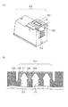
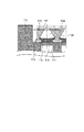
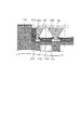
図3(a)は、一般的な記録ヘッド100の構成を示す斜視図である。また、図3(b)は、図3(a)の記録ヘッド100のチップ101におけるA−A’線上の断面図である。図3(b)に示すように、チップ101は支持部材110の凹部に配置されている。即ち、基板104が、支持部材110の凹部に配置されている。支持部材110は、樹脂やアルミナ等で形成されている。基板104は、接着剤112を介して支持部材110に接着されている。接着剤112はイオン重合反応機構により硬化する組成物、例えば紫外線硬化型エポキシ樹脂組成物等で形成されている。紫外線硬化型エポキシ樹脂組成物の中でも、遅延硬化性を持たせた樹脂組成物が好ましい。他に、光開始剤、反応性希釈剤の基本組成に加えてチクソ剤、シランカップリング剤、増感剤等の充填剤を含有してもよい。
FIG. 3A is a perspective view showing a configuration of a
支持部材110には開口部111が形成されており、開口部111の形状は供給口108の形状と対応している。インクは、開口部111から供給口108へと供給される。流路形成部材に形成されている流路117と供給口108とは連通している。よって、供給口108に供給されたインクは、次に供給口108から流路117へと供給される。
An
図3に示すような記録ヘッド100が、急激な環境変化、具体的には温度や湿度が急激に変化する環境下に晒された場合、図4に示すように、基板104に応力がかかる。これによって、基板104が変形することがある。例えば、流路形成部材105が収縮し、この収縮によって基板104に対して曲げ応力が働き、基板104が変形する。流路形成部材105が膨張した場合も同様である。他にも、接着剤112の収縮によって、基板104が変形する場合も考えられる。
When the
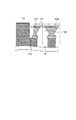
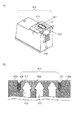
図5に、本発明の記録ヘッドの一例を示す。図5(a)は、本発明の記録ヘッド100の構成を示す斜視図である。図5(b)は、図5(a)の記録ヘッド100のチップ101におけるB−B’線上の断面図である。本発明の記録ヘッドは、基板104を貫通する供給口108の内部に、有機材料で形成された部材115を有する。この有機材料で形成された部材115は、基板104の梁構造の役割を果たす。部材115の下方には、部材115を支持する橋構造114が形成されていることが好ましい。橋構造114は、支持部材110の一部で形成してもよい。
FIG. 5 shows an example of the recording head of the present invention. FIG. 5A is a perspective view showing the configuration of the
部材115は、供給口108を形成し、供給口108を挟んで対向する2つの面(例えば面108aと面108b)をつないでいる。尚、供給口108を挟んで対向する2つの面とは、実質的な対向関係にある2つの面のことをいう。例えば、供給口108が円柱形状であった場合にも、円柱の側面を形成する部分のうち、対向している領域同士は、供給口108を挟んで対向する2つの面とする。対向する2つの面は、平行な関係にあることが好ましい。
The
図6に、本発明の記録ヘッドの基板104に応力がかかる状態を示す。図6に示すように、部材115が供給口108を挟んで対向する2つの面の間で梁構造の役割を果たす。従って、例えば接着剤112の収縮があったとしても、基板104の変形を抑制することができる。
FIG. 6 shows a state in which stress is applied to the
部材115がつなぐ2つの面は、供給口108が基板104を貫通する方向の上方からみたときに、供給口108の短手方向で対向する2つの面であることが好ましい。この2つの面とは、図5(b)でいう面108aと面108bである。一方で、供給口108が基板104を貫通する方向の上方からみたときに、部材115は、供給口108の長手方向で対向する2つの面をつないでいないことが好ましい。長手方向で対向する2つの面をつなぐと、インクの流れが良好でなくなる傾向にある。
The two surfaces connected by the
部材115は、有機材料で形成されている。部材115は記録材料に晒されるので、液体、特にインクに対する耐性が高いものであることが好ましい。例えば、ラジカル重合系のアクリル系樹脂組成物やイオン重合系のエポキシ系樹脂組成物であることが好ましい。部材115の大きさは、供給口108の寸法によるが、図6に示す断面の横幅が400μm以上1200μm以下であることが好ましい。また、図6に示す断面の上下方向の高さが50μm以上300μm以下であることが好ましい。部材115の図6の上下方向の高さは、インクの流れを考慮すると、供給口108の深さの70%以下であることが好ましく、50%以下であることがより好ましく、40%以下であることがさらに好ましい。また、梁構造としての強度の点から、5%以上であることが好ましく、10%以上であることがより好ましく、20%以上であることがさらに好ましい。尚、部材115の高さとは、供給口108の内部の部分と、図6に示す接着剤112の横の部分を合わせた部分の高さである。また、ここでの供給口108の深さとは、基板104の内部だけでなく、接着剤112の横の部分も合わせた深さである。また、製造過程を考慮すると、部材115は、供給口108の内部のうち、基板104の圧力発生素子106が形成されている側と反対側の面に近い側に形成されることが好ましい。
The
特に、接着剤112の収縮や膨張を考慮した場合には、部材115を形成する有機材料と接着剤112とは同じ材料で形成することが好ましい。同じ材料とは、分子量等までが一致する場合のみを意味するのではなく、例えば共にエポキシ樹脂であれば同じ材料と見なすことができる。より好ましくは、1つの材料を用いて、接着剤112と部材115を形成する。材料を合わせることで、力が打ち消し合うように働き、基板の変形をより良好に抑制することができる。
In particular, when the shrinkage and expansion of the adhesive 112 are taken into consideration, the organic material forming the
尚、図6に示すように温度や湿度が急激に変化する環境下において、部材115の縦弾性係数をE、断面二次モーメントをIとした時、曲げ応力に対する部材115の剛性Kは「K=E×I」と表すことができる。
As shown in FIG. 6, when the longitudinal elastic modulus of the
図7は、図5で説明したのと同様の記録ヘッドを示す図であるが、凹部を形成する支持部材の壁110aと基板104との間の領域が、封止材113で封止されている。封止材113は壁110aと基板104との間の領域の少なくとも一部に配置されていればよい。特には、供給口108が基板104を貫通する方向の上方(即ち、図7(b)においては上側の方向)からみたときに、基板104の長手方向に沿った側面を覆うように配置されていることが好ましい。
FIG. 7 is a view showing a recording head similar to that described with reference to FIG. 5, except that the region between the
図7に示すように封止材113が配置されている場合、封止材113の収縮によって、基板104に応力がかかる場合がある。図8に、封止材113が収縮する様子を示す。封止材113が収縮すると、曲げ応力とは異なる引張り力が基板104に働き、変形を誘発する。この結果、基板が変形することがある。また、封止材113が膨張した場合も同様である。
When the sealing
そこで、本発明では、図9、図10に示すように、基板104を貫通する供給口108の内部に、有機材料で形成された部材115を有する。部材115及びその周辺部分に関しては、図5、図6で説明したのと基本的に同様であるが、封止材113が形成されている場合には、封止材113の収縮、膨張に合わせて、部材115が収縮、膨張することができる。従って、基板104に対して発生する応力を良好に緩和することができる。
Therefore, in the present invention, as shown in FIGS. 9 and 10, a
特に、封止材113の収縮や膨張を考慮した場合には、部材115を形成する有機材料と封止材113とは同じ材料で形成することが好ましい。同じ材料とは、分子量等までが一致する場合のみを意味するのではなく、例えば共にエポキシ樹脂であれば同じ材料と見なすことができる。より好ましくは、1つの材料を用いて、封止材113と部材115を形成する。材料を合わせることで、力が打ち消し合うように働き、基板の変形をより良好に抑制することができる。特に、封止材113と部材115の材料を合わせた場合には、記録ヘッドの構造上、打ち消しの効果が顕著である。
In particular, in consideration of shrinkage and expansion of the sealing
図9の場合、急激な温度変化に対して発生する熱応力σは以下のようにして表すことができる。
σ=E×α×ΔT
σ:熱応力、E:縦弾性係数、α:線膨張係数、ΔT:温度変化
さらに、互いに拘束された異種材料間の面積をAとした場合に熱応力を起因として発生する外力Rは以下のようにして表すことができる。
R=σ×A
つまり、図9に示した流路形成部材105と部材115を同一線上とし、チップ101の短手方向の断面で見た場合に、流路形成部材105に発生する外力RXと部材115に発生する外力RYが同等であることが好ましい。部材による温度変化は大差ないことを考慮すると、封止材113の基板104の短手方向と平行な方向における断面積をAX、線膨張係数をαA、縦弾性係数をEA、有機材料で形成された部材115の基板104の短手方向と平行な方向における断面積をAY、線膨張係数をαB、縦弾性係数をEBとした場合に、以下の式を満たすことが好ましい。
(AX×αX×EX)/(AY×αY×EY)=0.8〜1.2
上記式を満たすことによって、図10に示すように封止材113の外力RXと部材115の外力RYが互いに作用しあい、緩和することで基板104の破損を抑制することができる。また、封止材113の外力と部材115の外力の割合が0.8以上1.2以下であれば、基板の変形が抑制しやすい。
In the case of FIG. 9, the thermal stress σ generated with respect to a rapid temperature change can be expressed as follows.
σ = E × α × ΔT
σ: thermal stress, E: longitudinal elastic modulus, α: linear expansion coefficient, ΔT: temperature change Further, when the area between dissimilar materials constrained to each other is A, the external force R generated due to the thermal stress is as follows: It can be expressed as follows.
R = σ × A
That is, the flow
(A X × α X × E X ) / (A Y × α Y × E Y ) = 0.8 to 1.2
By satisfying the above equation, mutually external force acts R Y are mutually external force R X and the
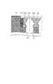
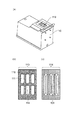
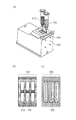
本発明の記録ヘッドの製造方法の一例を、図11、図12を用いて説明する。図11は記録ヘッド100の斜視図(a)と、支持部材の接合面116の拡大図(b)、接合面116に接着されるチップ101の裏面拡大図(c)である。接合面116には、基板104の供給口108に対応した形状の開口部111が開口している。また、接合面116には、橋構造114が形成されている。
An example of a method for manufacturing a recording head according to the present invention will be described with reference to FIGS. FIG. 11 is a perspective view (a) of the
このように、凹部が形成された支持部材を用意し、図12(a)、(b)に示すように、支持部材の接合面116の橋構造114の上に、有機材料で形成された部材115を塗布して形成する。そして、支持部材の橋構造114以外の部分の接合面116の少なくとも一部に、接着剤112を塗布して形成する。橋構造以外の部分としたのは、橋構造上には部材115が形成されている為である。
In this way, a support member in which a recess is formed is prepared. As shown in FIGS. 12A and 12B, a member formed of an organic material on the
続いて、図12(c)に示す基板104を、接合面116に接合させる。即ち、基板104を部材115上に配置するが、供給口108の内部に部材115が配置されるようにする。基板104と支持部材の接合面116とは、供給口108が形成された部分以外の部分で、接着剤112を介して接合される。
Subsequently, the
その後、必要に応じて封止材103、封止材113等を用いて封止を行い、加熱を行うことで、記録ヘッドが製造される。
Thereafter, sealing is performed using the sealing
以下、本発明を、実施例を用いてより具体的に説明する。 Hereinafter, the present invention will be described more specifically with reference to examples.
(実施例1)
まず、チップ101を以下の方法で製造した。
Example 1
First, the
シリコンからなる基板104上に、ポジ型感光性樹脂組成物(商品名;ODUR、東京応化工業製)をスピンコートで塗布した。これを露光、現像することで、インクの流路となる型材を形成した。次に、型材を覆うように、ネガ型感光性樹脂組成物(商品名:SU−8−3025、日本化薬製)をスピンコートにより塗布した。塗布したネガ型感光性樹脂組成物に、フォトマスクを介して露光を行った後、露光が行われなかった領域を現像液で除去することにより、吐出口109等をパターン形成した。
A positive photosensitive resin composition (trade name: ODUR, manufactured by Tokyo Ohka Kogyo Co., Ltd.) was applied onto a
次に、基板104に対し、熱酸化膜(不図示)をマスクとして水酸化テトラメチルアンモニウムによるウェットエッチングを行い、基板104を貫通する供給口108を形成した。続いて、型材を供給口108から溶出させた。このようにして、ネガ型感光性樹脂組成物から流路形成部材105を形成した。
Next, the
その後、チップ101と電気配線テープ102を接合させた。チップ101と電気配線テープ102の接合は、電気配線テープ102と基板104の電気信号入力端子107の表面に設けたAuとを熱圧着させている。
Thereafter, the
基板104の厚みは700μmであった。供給口108の短手方向の幅は500μmであった。
The thickness of the
以上のようにして製造したチップ101と電気配線テープ102とは、図11に示すように、アルミナからなる支持部材110上の接合面116に接着させた。
The
次に、図12に示すように、接着剤112を塗布し、さらに部材115を塗布した。具体的にはニードルによる描画塗布方法にてニードルを移動しながら接合面116上に接着剤112、橋構造114上に部材115を塗布した。接着剤112は、エポキシ樹脂組成物(商品名;KS−820、ADEKA製)で形成した。部材115は、接着剤112とは異なるエポキシ樹脂組成物(商品名;KR−827、ADEKA製)で形成した。接着剤112の厚みは150μm、部材115の厚みは200μmとした。
Next, as shown in FIG. 12, an adhesive 112 was applied, and a
次に、チップ101と電気配線テープ102を支持部材110に接合し、固定処理を行った。部材115は、供給口108を挟んで対向する2つの面をつなぐように配置された。そして、チップ101の周囲にブタジエン系エポキシ樹脂(商品名;NR200C、サンユレック製)を塗布し、110℃で加熱して硬化させた。このようにして、封止材103と封止材113とを形成した。封止材103及び封止材113については、図1に示すように、封止材103をチップ101の長手方向の両端部、封止材113をチップ101の短手方向の両端部に形成した。
Next, the
このようにして製造した記録ヘッド100の基板104を観察した結果、基板の変形は確認されなかった。
As a result of observing the
(実施例2)
実施例1では接着剤112と部材115の形成材料である有機材料とを異なる材料としたが、実施例2では、接着剤112と部材115の形成材料である有機材料とを同じ材料となるように、部材115の材料を変更した。即ち、接着剤112及び部材115を、エポキシ樹脂組成物(商品名;KS−820、ADEKA製)で形成した。接着剤112と部材115とを同じ材料で形成したので、ニードルも共通化し、接着剤112と部材115とを一括して形成した。これ以外は実施例1と同様にした。
(Example 2)
In the first embodiment, the adhesive 112 and the organic material that is the forming material of the
このようにして製造した記録ヘッド100の基板104を観察した結果、基板の変形は確認されなかった。
As a result of observing the
また、実施例1と比較すると、接着剤112の塗布と部材115の塗布を一括で行うことができる為、記録ヘッドをより少ない工程数で簡易に製造することができた。
In addition, compared with Example 1, since the adhesive 112 and the
(実施例3)
実施例1では封止材113と部材115の形成材料である有機材料とを異なる材料としたが、実施例3では、封止材113と部材115の形成材料である有機材料とを同じ材料となるように、部材115の材料を変更した。即ち、封止材113と部材115とを、ブタジエン系エポキシ樹脂(商品名;NR200C、サンユレック製)で形成した。封止材113と部材115とを同じ材料で形成したので、ニードルも共通化し、図13に示すようにして記録ヘッドを製造した。これ以外は実施例1と同様にした。
(Example 3)
In the first embodiment, the sealing
このようにして製造した記録ヘッド100の基板104を観察した結果、基板の変形は確認されなかった。
As a result of observing the
Claims (15)
前記基板には基板を貫通する供給口が形成されており、前記流路と前記供給口とは連通しており、
前記供給口の内部に、前記供給口を形成し前記供給口を挟んで対向する2つの面をつなぐ、有機材料で形成された部材が形成されていることを特徴とする記録ヘッド。 A recording head having a substrate and a flow path forming member for forming a flow path,
The substrate is formed with a supply port penetrating the substrate, and the flow path and the supply port are in communication with each other,
A recording head characterized in that a member made of an organic material is formed inside the supply port, the supply port being formed and connecting two surfaces facing each other across the supply port.
(AX×αX×EX)/(AY×αY×EY)=0.8〜1.2 The cross-sectional area of the sealing material in a direction parallel to the short direction of the substrate is AX , the linear expansion coefficient is α A , the longitudinal elastic modulus is E A , and the short side of the substrate of the member formed of the organic material 7. The recording head according to claim 5, wherein the following expression is satisfied, where A Y is a cross-sectional area in a direction parallel to the direction, α B is a linear expansion coefficient, and E B is a longitudinal elastic modulus.
(A X × α X × E X ) / (A Y × α Y × E Y ) = 0.8 to 1.2
前記有機材料で形成された部材を用意する工程と、
前記供給口の内部に前記有機材料で形成された部材が配置されるように、前記有機材料で形成された部材の上に基板を配置する工程と、
を有することを特徴とする記録ヘッドの製造方法。 A manufacturing method of a recording head according to claim 1,
Preparing a member formed of the organic material;
Disposing a substrate on the member formed of the organic material so that the member formed of the organic material is disposed inside the supply port;
A method for manufacturing a recording head, comprising:
The method for manufacturing a recording head according to claim 14, wherein the adhesive and the organic material are the same material, and the adhesive and the organic material are formed together.
Priority Applications (2)
| Application Number | Priority Date | Filing Date | Title |
|---|---|---|---|
| JP2014100913A JP6362406B2 (en) | 2014-05-14 | 2014-05-14 | Recording head |
| US14/708,018 US9358786B2 (en) | 2014-05-14 | 2015-05-08 | Recording head |
Applications Claiming Priority (1)
| Application Number | Priority Date | Filing Date | Title |
|---|---|---|---|
| JP2014100913A JP6362406B2 (en) | 2014-05-14 | 2014-05-14 | Recording head |
Publications (2)
| Publication Number | Publication Date |
|---|---|
| JP2015217543A true JP2015217543A (en) | 2015-12-07 |
| JP6362406B2 JP6362406B2 (en) | 2018-07-25 |
Family
ID=54537790
Family Applications (1)
| Application Number | Title | Priority Date | Filing Date |
|---|---|---|---|
| JP2014100913A Active JP6362406B2 (en) | 2014-05-14 | 2014-05-14 | Recording head |
Country Status (2)
| Country | Link |
|---|---|
| US (1) | US9358786B2 (en) |
| JP (1) | JP6362406B2 (en) |
Cited By (2)
| Publication number | Priority date | Publication date | Assignee | Title |
|---|---|---|---|---|
| JP2018008410A (en) * | 2016-07-13 | 2018-01-18 | キヤノン株式会社 | Liquid discharge head and liquid discharge apparatus |
| JP2019142216A (en) * | 2018-02-22 | 2019-08-29 | キヤノン株式会社 | Substrate of liquid ejection head and liquid ejection head |
Families Citing this family (1)
| Publication number | Priority date | Publication date | Assignee | Title |
|---|---|---|---|---|
| JP7166851B2 (en) * | 2018-09-07 | 2022-11-08 | キヤノン株式会社 | LIQUID EJECTION HEAD AND METHOD FOR MANUFACTURING LIQUID EJECTION HEAD |
Citations (6)
| Publication number | Priority date | Publication date | Assignee | Title |
|---|---|---|---|---|
| JP2003034027A (en) * | 2001-07-26 | 2003-02-04 | Sharp Corp | Ink jet head, its electrode connection structure, and method of manufacturing ink jet head |
| JP2007290203A (en) * | 2006-04-24 | 2007-11-08 | Canon Inc | Ink jet recording head and method for producing the same |
| JP2008265234A (en) * | 2007-04-24 | 2008-11-06 | Canon Inc | Ink jet recording head and method for producing the same |
| US20100020136A1 (en) * | 2008-07-25 | 2010-01-28 | Samsung Electronics Co., Ltd. | Inkjet printhead and method of manufacturing the same |
| JP2011093299A (en) * | 2009-06-16 | 2011-05-12 | Canon Inc | Liquid discharge head and method for manufacturing the same |
| JP2012187805A (en) * | 2011-03-10 | 2012-10-04 | Canon Inc | Inkjet recording head and method for manufacturing the same |
Family Cites Families (3)
| Publication number | Priority date | Publication date | Assignee | Title |
|---|---|---|---|---|
| JP2006035854A (en) | 2004-06-25 | 2006-02-09 | Canon Inc | Inkjet recording head manufacturing method, inkjet recording head, and substrate for recording head |
| JP5305691B2 (en) * | 2008-02-27 | 2013-10-02 | キヤノン株式会社 | Liquid discharge head and manufacturing method thereof |
| JP2009298108A (en) * | 2008-06-17 | 2009-12-24 | Canon Inc | Method for manufacturing inkjet recording head, and inkjet recording head |
-
2014
- 2014-05-14 JP JP2014100913A patent/JP6362406B2/en active Active
-
2015
- 2015-05-08 US US14/708,018 patent/US9358786B2/en active Active
Patent Citations (6)
| Publication number | Priority date | Publication date | Assignee | Title |
|---|---|---|---|---|
| JP2003034027A (en) * | 2001-07-26 | 2003-02-04 | Sharp Corp | Ink jet head, its electrode connection structure, and method of manufacturing ink jet head |
| JP2007290203A (en) * | 2006-04-24 | 2007-11-08 | Canon Inc | Ink jet recording head and method for producing the same |
| JP2008265234A (en) * | 2007-04-24 | 2008-11-06 | Canon Inc | Ink jet recording head and method for producing the same |
| US20100020136A1 (en) * | 2008-07-25 | 2010-01-28 | Samsung Electronics Co., Ltd. | Inkjet printhead and method of manufacturing the same |
| JP2011093299A (en) * | 2009-06-16 | 2011-05-12 | Canon Inc | Liquid discharge head and method for manufacturing the same |
| JP2012187805A (en) * | 2011-03-10 | 2012-10-04 | Canon Inc | Inkjet recording head and method for manufacturing the same |
Cited By (3)
| Publication number | Priority date | Publication date | Assignee | Title |
|---|---|---|---|---|
| JP2018008410A (en) * | 2016-07-13 | 2018-01-18 | キヤノン株式会社 | Liquid discharge head and liquid discharge apparatus |
| JP2019142216A (en) * | 2018-02-22 | 2019-08-29 | キヤノン株式会社 | Substrate of liquid ejection head and liquid ejection head |
| JP7183049B2 (en) | 2018-02-22 | 2022-12-05 | キヤノン株式会社 | LIQUID EJECTION HEAD SUBSTRATE AND LIQUID EJECTION HEAD |
Also Published As
| Publication number | Publication date |
|---|---|
| US9358786B2 (en) | 2016-06-07 |
| JP6362406B2 (en) | 2018-07-25 |
| US20150328891A1 (en) | 2015-11-19 |
Similar Documents
| Publication | Publication Date | Title |
|---|---|---|
| US8414110B2 (en) | Inkjet head | |
| US7523553B2 (en) | Method of manufacturing ink jet recording head | |
| WO2010143565A1 (en) | Liquid discharge recording head and method of manufacturing the same | |
| JP6362406B2 (en) | Recording head | |
| US10220619B2 (en) | MEMS device, head and liquid jet device | |
| WO2000058204A1 (en) | Narrow-pitch connector, pitch converter, micromachine, piezoelectric actuator, electrostatic actuator, ink-jet head, ink-jet printer, liquid crystal device, and electronic apparatus | |
| JP2016162999A (en) | Electronic device and method for manufacturing electronic device | |
| US7766455B2 (en) | Flexible adhesive materials for micro-fluid ejection heads and methods relating thereto | |
| JP2001322276A (en) | Ink jet recording head, ink jet recorder and method of making the head | |
| JP6548419B2 (en) | Liquid discharge head and method of manufacturing liquid discharge head | |
| JP6569359B2 (en) | Electronic device, liquid ejecting head, and manufacturing method of electronic device | |
| JP6275019B2 (en) | Print head containing two types of adhesive | |
| JP4461783B2 (en) | Method for manufacturing liquid jet head | |
| JP2011062866A (en) | Ink jet head | |
| US20250332831A1 (en) | Dry film membrane tenting | |
| JP6772807B2 (en) | Coating member peeling method and liquid injection head manufacturing method | |
| TWI555141B (en) | Semiconductor device and method for manufacturing semiconductor device | |
| JP2015024533A (en) | Liquid discharge head and driving method thereof | |
| KR101179320B1 (en) | Method for manufacturing inkjet head | |
| JP6546497B2 (en) | Thermal print head and thermal printer | |
| JP2024175448A (en) | Element substrate, liquid ejection head and their manufacturing methods | |
| WO2014077261A1 (en) | Inkjet head manufacturing method and inkjet head | |
| JP2015150827A (en) | Wiring mounting structure, manufacturing method of the same, liquid ejection head and liquid ejection device | |
| CN120588637A (en) | Liquid ejection head substrate, liquid ejection head, liquid ejection device, and method for manufacturing liquid ejection head substrate | |
| JP4646948B2 (en) | Inkjet recording head |
Legal Events
| Date | Code | Title | Description |
|---|---|---|---|
| A621 | Written request for application examination |
Free format text: JAPANESE INTERMEDIATE CODE: A621 Effective date: 20170502 |
|
| A977 | Report on retrieval |
Free format text: JAPANESE INTERMEDIATE CODE: A971007 Effective date: 20180122 |
|
| A131 | Notification of reasons for refusal |
Free format text: JAPANESE INTERMEDIATE CODE: A131 Effective date: 20180130 |
|
| A521 | Request for written amendment filed |
Free format text: JAPANESE INTERMEDIATE CODE: A523 Effective date: 20180330 |
|
| TRDD | Decision of grant or rejection written | ||
| A01 | Written decision to grant a patent or to grant a registration (utility model) |
Free format text: JAPANESE INTERMEDIATE CODE: A01 Effective date: 20180529 |
|
| A61 | First payment of annual fees (during grant procedure) |
Free format text: JAPANESE INTERMEDIATE CODE: A61 Effective date: 20180626 |
|
| R151 | Written notification of patent or utility model registration |
Ref document number: 6362406 Country of ref document: JP Free format text: JAPANESE INTERMEDIATE CODE: R151 |