JP2015202035A - Gate drive circuit of voltage-driven power semiconductor device - Google Patents
Gate drive circuit of voltage-driven power semiconductor device Download PDFInfo
- Publication number
- JP2015202035A JP2015202035A JP2015056560A JP2015056560A JP2015202035A JP 2015202035 A JP2015202035 A JP 2015202035A JP 2015056560 A JP2015056560 A JP 2015056560A JP 2015056560 A JP2015056560 A JP 2015056560A JP 2015202035 A JP2015202035 A JP 2015202035A
- Authority
- JP
- Japan
- Prior art keywords
- circuit
- voltage
- power semiconductor
- short
- time
- Prior art date
- Legal status (The legal status is an assumption and is not a legal conclusion. Google has not performed a legal analysis and makes no representation as to the accuracy of the status listed.)
- Granted
Links
Images


Classifications
-
- Y—GENERAL TAGGING OF NEW TECHNOLOGICAL DEVELOPMENTS; GENERAL TAGGING OF CROSS-SECTIONAL TECHNOLOGIES SPANNING OVER SEVERAL SECTIONS OF THE IPC; TECHNICAL SUBJECTS COVERED BY FORMER USPC CROSS-REFERENCE ART COLLECTIONS [XRACs] AND DIGESTS
- Y02—TECHNOLOGIES OR APPLICATIONS FOR MITIGATION OR ADAPTATION AGAINST CLIMATE CHANGE
- Y02B—CLIMATE CHANGE MITIGATION TECHNOLOGIES RELATED TO BUILDINGS, e.g. HOUSING, HOUSE APPLIANCES OR RELATED END-USER APPLICATIONS
- Y02B70/00—Technologies for an efficient end-user side electric power management and consumption
- Y02B70/10—Technologies improving the efficiency by using switched-mode power supplies [SMPS], i.e. efficient power electronics conversion e.g. power factor correction or reduction of losses in power supplies or efficient standby modes
Abstract
Description
本発明は、IGBTなどの電圧駆動形パワー半導体素子を駆動するゲート駆動回路における過電流保護方式に関する。 The present invention relates to an overcurrent protection system in a gate drive circuit that drives a voltage-driven power semiconductor element such as an IGBT.
図5に、電圧駆動型パワー半導体スイッチング素子としてIGBTを用いたインバータシステムの主回路図例を示す。1が直流電源回路(交流電源入力の場合は、交流電源1cを入力とする整流器1aと大容量コンデンサ1bとから構成され、その電圧値をEdとする)。2が直流電圧を交流に変換するIGBT及びダイオードより構成するインバータ回路、3がIGBTのゲート駆動回路(各素子に接続)、4がIGBT、5が逆並列に接続されているダイオード、6が電動機などの負荷である。ここで、インバータ回路は三相インバータの場合、6個のアームで構成されるが、各アームとも構成は同じであるので、1アームのみ部品記号を付与している。また、7がIGBTをオンオフさせるための制御信号(各ゲート駆動回路に入力)で、制御回路8より各IGBTのゲート駆動回路に出力される。
FIG. 5 shows an example of a main circuit diagram of an inverter system using an IGBT as a voltage-driven power semiconductor switching element.
図6に、IGBTが過電流となった場合に強制遮断を実施する機能を有したゲート駆動回路3の詳細回路図を示す。9が本回路のゲート駆動電源、10及び11がIGBT4をターンオン及びターンオフさせるためのトランジスタなどのスイッチ素子で、本図の場合ターンオン側10がNPNトランジスタ、ターンオフ側11がPNPトランジスタを用いたコンプリメンタリー接続回路で構成され、フォトカプラなどの絶縁器12を介した信号13によって相補的に動作する。本図の場合は、信号13がH(ハイ)になるとトランジスタ10がオンし、その結果IGBT4のゲートに電流が流れ込み、IGBT4がオンする。一方、信号13がLの場合はPNPトランジスタ11がオンすることで、IGBT4に蓄積しているゲート電荷が放電する方向に電流が流れ、IGBT4がオフする。また14がオン側のゲート電流制限用のゲート抵抗、15がオフ側のゲート電流制限用のゲート抵抗で、抵抗値によってスイッチングのスピードを調整する。16(16a、16b)がトランジスタ10、11のベース抵抗で、17、18が通常動作時における電流バイパス用のダイオードである。
FIG. 6 shows a detailed circuit diagram of the gate driving circuit 3 having a function of forcibly blocking when the IGBT becomes overcurrent. 9 is a gate drive power supply of this circuit, 10 and 11 are switch elements such as transistors for turning on and off the IGBT 4, and in this case, the turn-on
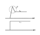
図9に通常動作時におけるIGBTがターンオンする時のコレクタ電流(IC)とゲート・エミッタ間電圧波形(VGE)例を示す。上下アームの場合の例で、オン信号指令によりゲート電圧VGEが立上ると、コレクタ電流Icは負荷電流にダイオードの逆回復電流28重畳された波形となる。
FIG. 9 shows an example of the collector current (I C ) and the gate-emitter voltage waveform (V GE ) when the IGBT is turned on during normal operation. In the case of the upper and lower arms, when the gate voltage V GE rises due to the ON signal command, the collector current Ic has a waveform in which the
また、図7には、インバータ回路の上下アームのいずれかのIGBTがアーム短絡故障破壊した場合の動作図を示す。短絡故障したIGBTQdの対向アーム側のIGBTQuにオン指令を入力すると、直流電源短絡状態となり、破線で示す経路で過大な短絡電流(通常IGBTの定格電流の5〜10倍程度)が流れる。一方、IGBTは短絡耐量時間(一般的には10μs程度)や許容される短絡エネルギーがあり、本時間内に定格電流に収まるように遮断できれば、短絡保護が可能となる。 FIG. 7 shows an operation diagram when one of the upper and lower arms of the inverter circuit breaks down due to an arm short circuit failure. When an ON command is input to the IGBT Qu on the opposite arm side of the IGBT Qd that has undergone a short circuit failure, a DC power supply is short-circuited, and an excessive short circuit current (about 5 to 10 times the rated current of the normal IGBT) flows through a path indicated by a broken line. On the other hand, the IGBT has a short-circuit withstand time (generally about 10 μs) and an allowable short-circuit energy, and short-circuit protection is possible if it can be cut off so as to be within the rated current within this time.
図6において上記説明した以外の回路は短絡保護を実施するための回路で、21はIGBTチップ内に設けられたIGBTに流れている電流を検出するためのセンスIGBTである。一般に本センスIGBTは、主IGBTに対して1/1000程度の比率(正確な比率はIGBTチップ設計の時点で設定する)で電流が流れる。 In FIG. 6, a circuit other than that described above is a circuit for implementing short circuit protection, and 21 is a sense IGBT for detecting a current flowing in the IGBT provided in the IGBT chip. In general, current flows in the sense IGBT at a ratio of about 1/1000 with respect to the main IGBT (the exact ratio is set at the time of designing the IGBT chip).
本センスIGBT21と直列に抵抗22を接続し、抵抗22に発生する電圧23を検出することで主IGBT4に流れている電流を間接的に検出することが可能となる。従って、電圧23をコンパレータ回路25に入力し、電圧設定器33の設定値と比較してその設定値以上であった場合は過電流状態、あるいは電源短絡(アーム短絡)状態であると判断し、信号ラッチ用SRフリップフロップ回路35を介してスイッチ回路24のオンによって強制遮断を行うことでIGBTの保護が可能となる。但しこの時、大電流遮断を行うので、高ゲート抵抗による遮断や、ゲート・エミッタ間電圧を徐々に低下させる方式(図6の回路方式)などによって、ソフト遮断動作を実施する必要がある。図10に本回路を適用した場合のアーム短絡時の各部波形図例を示す。NPNトランジスタ10がオフ、PNPトランジスタ11がオンすることでIGBT4が強制遮断される。但しこのとき、コンデンサ26が接続されているため、点Pの電位は即刻低下するのではなく、抵抗27とコンデンサ26との放電時定数によって、ある時間を有して低下する。そのためIGBTのゲート部(VGE)にもほぼ同様の波形が印加され、その期間コレクタ電流遮断の電流変化率(−di/dt)が制限され、大きなターンオフサージ電圧(VCEpeak)が発生しないソフト遮断化が図れる。図10にこれら一連の概略的な波形図(コレクタ電流IC、コレクタ・エミッタ間電圧VCE、ゲート・エミッタ間電圧VGE)を示す。 短絡電流Icが流れるとIGBTに印加される電圧VCEは直流電源電圧Edから配線のインダクタンスによる電圧低下分を差し引いた電圧となる。また、短絡電流がICpeakに到達してゲート信号を遮断するとゲート電圧VGEはソフト遮断動作により所定の時定数で低下する。この結果、電流低減率(−di/dt)が緩やかになり、電圧上昇率(dv/dt)も緩やかになり、IGBTに印加されるサージ電圧(VCEpeak)は低い値に抑制される。
By connecting the
これらの回路により、IGBTの上下アーム短絡などの過電流状態からの保護が可能となる。
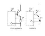
また図6に示す以外の過電流状態を検出する方法を図8に示す。図8(a)がIGBTQ1と直列にシャント抵抗SRを接続する方式、図8(b)がIGBTQ1と直列にCTなどの電流検出器を接続する方式である。各ゲート駆動回路GD1、GD2では各検出器からの検出量を電流値に応じた電圧に変換して、この電圧が所定値以上になった場合に図6の回路のスイッチ回路24をオンする方式である。基本的には検出値がある閾値以上となった場合は過電流状態であると判断し、強制遮断を実施するということで、図6の場合と同様の動作となる。
These circuits enable protection from an overcurrent state such as a short circuit between the upper and lower arms of the IGBT.
FIG. 8 shows a method for detecting an overcurrent state other than that shown in FIG. FIG. 8A shows a system in which a shunt resistor SR is connected in series with the IGBT Q1, and FIG. 8B shows a system in which a current detector such as CT is connected in series with the IGBT Q1. Each gate drive circuit GD1, GD2 converts the detection amount from each detector into a voltage corresponding to the current value, and turns on the
また、図6に示す過電流検出とソフト遮断回路を含んだゲート駆動回路例は、特許文献1、特許文献2などに掲載されている。
Examples of the gate drive circuit including the overcurrent detection and soft cutoff circuit shown in FIG. 6 are described in
上述のように、アーム短絡発生時、IGBTは許容される短絡耐量時間やエネルギー耐量以内に遮断しなければならないため、速やかなアーム短絡状態の検出と、大電流遮断時におけるサージ電圧の低減を図ったソフト遮断化が必要となる。
速やかな短絡電流検出を行うためには、その検出値を低くすればよいが、一方で通常ターンオン時に発生するダイオードの逆回復電流(図9中の28:IGBTやダイオードの特性、およびゲート駆動条件によっても異なるが、瞬間的に負荷電流の2倍程度流れることもありうる)は短絡電流ではないので過電流として検出してはならず、さらに電流検出器の検出ばらつきも考慮しなければならないため、実際の設定値はシステムの最大電流値の数倍程度のところに設定する必要がある。
As described above, when an arm short-circuit occurs, the IGBT must be shut off within the allowable short-circuit tolerance time and energy tolerance. Therefore, the arm short-circuit state is detected quickly and the surge voltage is reduced when a large current is interrupted. It is necessary to turn off the software.
In order to detect the short-circuit current promptly, the detection value may be lowered. On the other hand, the reverse recovery current of the diode normally generated at the time of turn-on (28 in FIG. 9: characteristics of the IGBT and the diode, and the gate drive condition) (Although it may vary depending on the load current, it may flow about twice the load current instantaneously) is not a short-circuit current, so it must not be detected as an overcurrent, and the detection variation of the current detector must also be taken into account. The actual set value needs to be set at several times the maximum current value of the system.
さらに、実際は過電流検出されてから遮断動作が始まるまでは、回路上の遅延時間や、ゲートチャージ電荷の引き抜きなどにある程度時間を要するために、その間も電流が増加して流れ続ける場合もある(図10中のΔt)。さらに、遮断時のdi/dtによって発生するサージ電圧(VCEpeak)も規定値以下にする必要があるため、短時間で遮断しなければならないこととトレードオフ的に時間を掛けたソフト遮断化が必要となる。
以上のように短絡時における保護遮断をある程度余裕をもって適切に実施しないと、短絡耐量時間や短絡耐量エネルギーのオーバーや、サージ電圧過大になり、素子破壊を招く。
また、センスIGBTによる電流検出方式は、主IGBTの電流に対する電流比率が1/1000程度であるため、IGBTのターンオンやターンオフなどの過渡状態時は、センスIGBTおよび直列接続された電流検出用抵抗部に高い周波数成分を持ったノイズが印加(図11にターンオン時においてノイズが重畳した電流検出信号波形例を示す、またアーム短絡時の電流波形も同様な波形となる)され、瞬時電流値の正確な測定ができない課題を有する。そのため一般的には、ターンオンの過渡現象が終了するまでの時間(数100ns〜数μs)は、過電流の非検出期間とすることが行われる。
Furthermore, since a certain amount of time is required for the delay time on the circuit and the extraction of the gate charge charges after the overcurrent is detected until the interruption operation is actually started, the current may continue to increase during that time ( Δt in FIG. Furthermore, since the surge voltage (V CEpeak ) generated by di / dt at the time of interruption needs to be less than the specified value, it is necessary to cut off in a short time, and soft interruption over time in a trade-off manner. Necessary.
As described above, if the protective interruption at the time of short circuit is not properly performed with a certain margin, the short circuit withstand time, short circuit withstand energy will be exceeded, surge voltage will be excessive, and the element will be destroyed.
Further, the current detection method using the sense IGBT has a current ratio of about 1/1000 to the current of the main IGBT. Therefore, in a transient state such as turn-on or turn-off of the IGBT, the sense IGBT and the current detection resistor unit connected in series A noise having a high frequency component is applied (FIG. 11 shows an example of a current detection signal waveform in which noise is superimposed at the time of turn-on, and the current waveform when the arm is short-circuited is also similar), and the instantaneous current value is accurately measured. There is a problem that cannot be measured easily. Therefore, generally, the time until the turn-on transient is completed (several hundred ns to several μs) is set as the overcurrent non-detection period.
本現象に対しては、電流検出をしない非検出期間を長くしたり、時定数が長いフィルタ回路を接続すれば、正確に過電流状態を検出することが可能となるが、その分IGBTを遮断するまでの時間が長くなる。一方非検出時間を短くすると、ノイズによる誤動作検知の可能性が高いというトレードオフ特性となる。
従って、本発明の課題は、スイッチング時の過渡状態で大きなノイズ信号が重畳された電流の立上り期間においても、過電流状態を検出可能な方式とし、速やかなアーム短絡検出を可能とした信頼性の高い短絡保護方式を提供することである。
For this phenomenon, if a non-detection period in which no current is detected is extended or a filter circuit with a long time constant is connected, an overcurrent state can be detected accurately, but the IGBT is cut off accordingly. The time to do becomes longer. On the other hand, if the non-detection time is shortened, a trade-off characteristic that the possibility of malfunction detection due to noise is high.
Therefore, an object of the present invention is to provide a method capable of detecting an overcurrent state even during a rising period of a current in which a large noise signal is superimposed in a transient state at the time of switching. It is to provide a high short circuit protection scheme.
上述の課題を解決するために、第1の発明においては、電力変換器に適用する電圧駆動形パワー半導体素子を駆動するゲート駆動回路において、前記パワー半導体素子に流れている短絡電流を検出する短絡電流検出手段と、前記電流検出値を積分する短絡電流積分手段とを設け、前記短絡電流積分手段の積分値が設定値以上であった場合、強制的にゲート遮断する。 In order to solve the above-described problem, in the first invention, in a gate drive circuit for driving a voltage-driven power semiconductor element applied to a power converter, a short circuit for detecting a short-circuit current flowing in the power semiconductor element. A current detection means and a short-circuit current integration means for integrating the current detection value are provided. When the integration value of the short-circuit current integration means is equal to or greater than a set value, the gate is forcibly cut off.
第2の発明においては、第1の発明における電圧駆動形パワー半導体素子のゲート駆動回路において、前記短絡電流積分手段の積分範囲は電圧駆動形パワー半導体素子がターンオン開始時点からある設定された積分時間までとする。 In the second invention, in the gate drive circuit of the voltage-driven power semiconductor element in the first invention, the integration range of the short-circuit current integrating means is a set integration time from the time when the voltage-driven power semiconductor element is turned on. Up to.
第3の発明においては、第2の発明における電圧駆動形パワー半導体素子のゲート駆動回路において、前記ターンオン開始時点からある設定された積分時間は前記電圧駆動形パワー半導体素子の短絡許容時間以内とする。 In a third aspect of the invention, in the gate drive circuit for a voltage-driven power semiconductor element according to the second aspect of the invention, a set integration time from the turn-on start time is within an allowable short-circuit time of the voltage-driven power semiconductor element. .
第4の発明においては、第1の発明における電圧駆動形パワー半導体素子のゲート駆動回路における、前記短絡電流積分手段の積分開始時刻をターンオン開始時点からある設定された時間後とする。 In the fourth invention, the integration start time of the short-circuit current integrating means in the gate drive circuit of the voltage-driven power semiconductor element in the first invention is a set time after the turn-on start time.
第5の発明においては、第4の発明における前記短絡電流積分手段の積分終了時刻は、ターンオン開始時点からの時間が前記電圧駆動形パワー半導体素子の短絡許容時間以内となる時刻とする。 In the fifth invention, the integration end time of the short-circuit current integrating means in the fourth invention is a time when the time from the turn-on start time is within the short-circuit allowable time of the voltage-driven power semiconductor element.
第6の発明においては、第1〜第5の発明における前記電圧駆動形パワー半導体素子のゲート駆動回路で駆動する前記パワー半導体素子にワイドバンドギャップ半導体材料を適用したパワー半導体素子を用いることを特徴とする。 In a sixth aspect of the present invention, a power semiconductor element in which a wide band gap semiconductor material is applied to the power semiconductor element driven by the gate driving circuit of the voltage-driven power semiconductor element in the first to fifth aspects is used. And
第7の発明においては、第6の発明におけるワイドバンドギャップ半導体材料は、炭化珪素、窒化ガリウム、酸化ガリウム又はダイアモンドの何れか1種又は複数種の組合せで構成することを特徴とする。 In a seventh aspect, the wide band gap semiconductor material according to the sixth aspect is characterized by being composed of one or a combination of any of silicon carbide, gallium nitride, gallium oxide and diamond.
本発明では、パワー半導体素子に流れる短絡電流を検出する短絡電流検出手段と、前記電流検出値を積分する短絡電流積分手段とを設け、前記短絡電流積分手段の積分値が設定値以上であった場合、強制的にゲート遮断する方式としている。その結果、スイッチング時の過渡状態で大きなノイズ信号が重畳した電流の立上り期間においても、過電流状態が検出可能となり、従来アーム短絡誤検知防止のために設けていた非検出時間を短くする又はなくすることができるので、速やかなアーム短絡検出が可能となる。その結果、信頼性の高い短絡保護が可能となる。
さらに、電圧駆動形パワー半導体素子として、炭化珪素などのワイドバンドギャップ半導体材料からなるMOSFET、IGBTなどのスイッチング素子を適用することにより、ゲート駆動電圧を低下させる際に、主回路電流であるドレイン電流又はコレクタ電流を高速に低減でき、短絡電流とサージ電圧をより低減できる効果が得られる。
In the present invention, a short-circuit current detecting means for detecting a short-circuit current flowing in the power semiconductor element and a short-circuit current integrating means for integrating the current detection value are provided, and the integrated value of the short-circuit current integrating means is equal to or greater than a set value. In this case, the gate is forcibly shut off. As a result, it is possible to detect an overcurrent state even during a current rising period in which a large noise signal is superimposed in a transient state at the time of switching, and the conventional non-detection time provided to prevent erroneous detection of an arm short circuit is shortened or eliminated. Therefore, it is possible to quickly detect an arm short circuit. As a result, highly reliable short circuit protection is possible.
Further, by applying a switching element such as a MOSFET or IGBT made of a wide band gap semiconductor material such as silicon carbide as a voltage-driven power semiconductor element, a drain current which is a main circuit current when the gate driving voltage is reduced. Alternatively, the collector current can be reduced at a high speed, and the short-circuit current and the surge voltage can be further reduced.
本発明の要点は、電力変換器に適用する電圧駆動形パワー半導体素子を駆動するゲート駆動回路において、前記パワー半導体素子に流れる短絡電流を検出する短絡電流検出手段と、前記電流検出値を積分する短絡電流積分手段とを設け、前記短絡電流積分手段の積分値が設定値以上となった場合、強制的にゲート遮断する点である。 The gist of the present invention is that in a gate drive circuit for driving a voltage-driven power semiconductor element applied to a power converter, a short-circuit current detecting means for detecting a short-circuit current flowing in the power semiconductor element, and integrating the detected current value Short-circuit current integrating means is provided, and when the integrated value of the short-circuit current integrating means exceeds a set value, the gate is forcibly cut off.
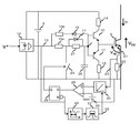
図1に、本発明の第1の実施例を示す。 図6の従来回路例に対し、センスIGBT21で検出した電流を抵抗22で電圧に変換した電流検出信号23を積分する積分回路30と、積分回路30の動作期間を決める積分時間設定回路31を追加した構成である。従来回路と同じ部分については説明を省略する。
FIG. 1 shows a first embodiment of the present invention. An
積分時間を設定するためのワンショット回路31はゲート駆動指令信号13の立ち上がりをトリガにして積分時間となるti分のパルスを形成し、積分回路30に入力(信号32)する。積分回路30は信号32の入力を受けて、センスIGBT21で検出した電流相当の電圧23を積分する。この積分値がti期間内に電圧設定器33の設定値(Qdet)以上となったことがコンパレータ回路25で判定されると、アーム短絡電流が流れていると判断し、信号のラッチを目的としたSRフリップ回路35を介してスイッチ回路24を動作させ、強制遮断を行う。ここで積分時間tiは、保護対象となるIGBTの短絡耐量時間より短くする必要がある。
Integration time one-
図2に本回路によるアーム短絡時における動作波形例を示す。IGBTの電流Icの積分波形が設定器33の設定値(Qdet)に到達した時点でゲート信号を遮断し、ゲート電圧VGEは緩やかに低下していることがわかる。電流検出に積分回路30を用いているため、図11に示すようなノイズが重畳された波形の場合でも安定した検出が可能となる。また、この例ではソフト遮断の例を示しているが、ソフト遮断でなくても、配線インダクタンスの低減、スナバ回路の強化などにより、ハード遮断の場合でも適用可能である。
FIG. 2 shows an example of operation waveforms when the arm is short-circuited by this circuit. It can be seen that the gate signal is cut off when the integrated waveform of the IGBT current Ic reaches the set value (Q det ) of the
図3に本発明の第2の実施例を示す。第1の実施例に対し、積分動作を開始するまでの時間を決めるためのオンディレータイマー回路34を追加した構成である。オンディレータイマー回路34はゲート駆動指令信号13の立上がり時刻を遅延(td分)する回路である。回路31は遅延回路34からの出力信号をトリガに積分時間となるti分のパルスを形成し、積分回路30に入力(信号32)する。積分回路30は信号32の入力を受けて、センスIGBTの電流相当の電圧23を積分する。この積分された電圧がti期間内に電圧設定器33の電圧(Qdet)以上となった場合はアーム短絡電流が流れていると判断し、SRフリップ回路35を介してスイッチ回路24を動作させ、強制遮断を行う。ここで、積分を開始するまでの遅延時間tdと積分時間tiとの和(td+ti)は、保護対象となるIGBTの短絡耐量時間より短くする必要がある。
FIG. 3 shows a second embodiment of the present invention. The on-
図4に、本回路によるアーム短絡時における動作波形例を示す。オンディレータイマー回路34の遅れ時間tdの期間では積分回路30は積分動作をせず、積分開始時点から積分時間tiの期間内に積分値が電圧設定器33の電圧(Qdet)になった時点でゲート電圧VGEを緩やかに低下させて遮断する実施例である。ターンオン時、図11に示すようにダイオードの逆回復電流が負荷電流に重畳され、この波形にノイズが重畳した波形(図11)を積分すると、短絡過電流でない電流波形を積分することになり、積分値が短絡過電流を示す値と異なる結果となる。これを回避するために、オン信号時オンディレータイマー回路34の遅れ時間tdの期間は積分動作をしないようにしたものである。また、この例ではソフト遮断の例を示しているが、ソフト遮断でなくても、配線インダクタンスの低減、スナバ回路の強化などにより、ハード遮断の場合でも適用可能である。
FIG. 4 shows an example of operation waveforms when the arm is short-circuited by this circuit. During the period of the delay time td of the on-
尚、上記実施例にはスイッチング素子としてIGBTを用いた例を示したが、スイッチング素子としてはMOSFETなどの電圧駆動型の素子でも実現可能である。特に、電圧駆動形パワー半導体素子として、炭化珪素などのワイドバンドギャップ半導体材料からなるMOSFET、IGBTなどのスイッチング素子を適用することにより、ゲート駆動電圧を低下させる際に、主回路電流であるドレイン電流又はコレクタ電流を高速に低減できる効果が得られる。 In the above embodiment, an IGBT is used as the switching element. However, the switching element can be realized by a voltage driven element such as a MOSFET. In particular, when a gate drive voltage is lowered by applying a switching element such as a MOSFET or IGBT made of a wide band gap semiconductor material such as silicon carbide as a voltage-driven power semiconductor element, a drain current which is a main circuit current Or the effect which can reduce a collector current at high speed is acquired.
本発明は、半導体スイッチング素子を適用した変換装置における過電流保護機能を備えたゲート駆動回路に関する提案であり、電動機駆動用インバータ、無停電電源装置、直流電源装置などへの適用が可能である。 The present invention is a proposal related to a gate drive circuit having an overcurrent protection function in a conversion device to which a semiconductor switching element is applied, and can be applied to an inverter for driving a motor, an uninterruptible power supply, a DC power supply, and the like.
1・・・直流電源 1b・・・大容量コンデンサ 2・・・インバータ
3、GD1、GD2・・・ゲート駆動回路 6・・・電動機(負荷)
4、Qu、Qd、Q1・・・IGBT 21・・・センスIGBT
5、17、18・・・ダイオード 7・・・駆動信号
8・・・制御回路 34・・・オンディレータイマー回路
9・・・ゲート駆動電源 10・・・NPNトランジスタ
11・・・PNPトランジスタ 12・・・フォトカプラ
14、15、16a、16b、27、22・・・抵抗 26・・・コンデンサ
24・・・スイッチ回路 25・・・コンパレータ回路
33・・・電圧設定器 35・・・SRフリップフロップ
SR・・・シャント抵抗 CT・・・電流検出器
30・・・積分器 31・・・ワンショット回路
DESCRIPTION OF
4, Qu, Qd, Q1 ...
5, 17, 18 ... Diode 7 ... Drive signal 8 ...
Claims (7)
7. The gate drive circuit for a voltage-driven power semiconductor device according to claim 6, wherein the wide band gap semiconductor material is composed of one or a combination of any of silicon carbide, gallium nitride, gallium oxide and diamond. A gate drive circuit of a voltage drive type power semiconductor element characterized by the above.
Priority Applications (1)
| Application Number | Priority Date | Filing Date | Title |
|---|---|---|---|
| JP2015056560A JP6525141B2 (en) | 2014-04-02 | 2015-03-19 | Gate drive circuit for voltage driven power semiconductor device |
Applications Claiming Priority (3)
| Application Number | Priority Date | Filing Date | Title |
|---|---|---|---|
| JP2014076189 | 2014-04-02 | ||
| JP2014076189 | 2014-04-02 | ||
| JP2015056560A JP6525141B2 (en) | 2014-04-02 | 2015-03-19 | Gate drive circuit for voltage driven power semiconductor device |
Publications (2)
| Publication Number | Publication Date |
|---|---|
| JP2015202035A true JP2015202035A (en) | 2015-11-12 |
| JP6525141B2 JP6525141B2 (en) | 2019-06-05 |
Family
ID=54552844
Family Applications (1)
| Application Number | Title | Priority Date | Filing Date |
|---|---|---|---|
| JP2015056560A Expired - Fee Related JP6525141B2 (en) | 2014-04-02 | 2015-03-19 | Gate drive circuit for voltage driven power semiconductor device |
Country Status (1)
| Country | Link |
|---|---|
| JP (1) | JP6525141B2 (en) |
Cited By (3)
| Publication number | Priority date | Publication date | Assignee | Title |
|---|---|---|---|---|
| JP2017122631A (en) * | 2016-01-07 | 2017-07-13 | 株式会社 日立パワーデバイス | Current detector and semiconductor device using the current detector |
| JP2017139622A (en) * | 2016-02-03 | 2017-08-10 | 株式会社東芝 | Gate control circuit and power supply circuit |
| WO2024058277A1 (en) * | 2022-09-15 | 2024-03-21 | 株式会社Flosfia | Power conversion circuit and control system |
Citations (4)
| Publication number | Priority date | Publication date | Assignee | Title |
|---|---|---|---|---|
| JP2004312907A (en) * | 2003-04-09 | 2004-11-04 | Fuji Electric Fa Components & Systems Co Ltd | Gate drive circuit of power semiconductor device |
| JP2007259533A (en) * | 2006-03-22 | 2007-10-04 | Hitachi Ltd | Protective circuit for semiconductor element |
| JP2009055200A (en) * | 2007-08-24 | 2009-03-12 | National Institute Of Advanced Industrial & Technology | Controller and control method for silicon carbide static induction transistor |
| JP2011130564A (en) * | 2009-12-17 | 2011-06-30 | Hitachi Ltd | Apparatus and method for protecting power semiconductor switch element |
-
2015
- 2015-03-19 JP JP2015056560A patent/JP6525141B2/en not_active Expired - Fee Related
Patent Citations (4)
| Publication number | Priority date | Publication date | Assignee | Title |
|---|---|---|---|---|
| JP2004312907A (en) * | 2003-04-09 | 2004-11-04 | Fuji Electric Fa Components & Systems Co Ltd | Gate drive circuit of power semiconductor device |
| JP2007259533A (en) * | 2006-03-22 | 2007-10-04 | Hitachi Ltd | Protective circuit for semiconductor element |
| JP2009055200A (en) * | 2007-08-24 | 2009-03-12 | National Institute Of Advanced Industrial & Technology | Controller and control method for silicon carbide static induction transistor |
| JP2011130564A (en) * | 2009-12-17 | 2011-06-30 | Hitachi Ltd | Apparatus and method for protecting power semiconductor switch element |
Cited By (3)
| Publication number | Priority date | Publication date | Assignee | Title |
|---|---|---|---|---|
| JP2017122631A (en) * | 2016-01-07 | 2017-07-13 | 株式会社 日立パワーデバイス | Current detector and semiconductor device using the current detector |
| JP2017139622A (en) * | 2016-02-03 | 2017-08-10 | 株式会社東芝 | Gate control circuit and power supply circuit |
| WO2024058277A1 (en) * | 2022-09-15 | 2024-03-21 | 株式会社Flosfia | Power conversion circuit and control system |
Also Published As
| Publication number | Publication date |
|---|---|
| JP6525141B2 (en) | 2019-06-05 |
Similar Documents
| Publication | Publication Date | Title |
|---|---|---|
| JP6582471B2 (en) | Gate drive circuit for voltage-driven power semiconductor device | |
| JP3883925B2 (en) | Power semiconductor element drive circuit | |
| JP6190280B2 (en) | Semiconductor drive device and power conversion device using the same | |
| KR101662471B1 (en) | Drive protection circuit, semiconductor module, and automobile | |
| JP2669117B2 (en) | Drive circuit for voltage-driven semiconductor devices | |
| WO2017141545A1 (en) | Overcurrent protection device for semiconductor element | |
| CN108809059B (en) | Driving device for semiconductor element | |
| JP2009225506A (en) | Power converter | |
| JP6070853B2 (en) | Insulated gate semiconductor device | |
| JPWO2013008452A1 (en) | Short circuit protection circuit | |
| Bertelshofer et al. | Design rules to adapt the desaturation detection for SiC MOSFET modules | |
| JP2018057105A (en) | Semiconductor drive device and power converter using the same | |
| JP2014127728A (en) | Short circuit fault protection device and short circuit fault protection method | |
| JP6525141B2 (en) | Gate drive circuit for voltage driven power semiconductor device | |
| JP7087371B2 (en) | Semiconductor devices and power modules | |
| JP2018011467A (en) | Gate drive circuit for semiconductor switching element | |
| JP6758538B2 (en) | Protection circuit and power module for power semiconductor devices | |
| JP6394036B2 (en) | Driving device for power semiconductor element | |
| JP2014217151A (en) | Power conversion device and overcurrent protection method for the same | |
| JP6070003B2 (en) | Semiconductor drive device | |
| KR100807547B1 (en) | A drive circuit of a semiconductor switch for an inverter | |
| JP4413482B2 (en) | Power semiconductor element drive circuit | |
| Bakran et al. | Integrating the New 2D—Short circuit detection method into a power module with a power supply fed by the gate voltage | |
| JP6298735B2 (en) | Semiconductor drive device and power conversion device using the same | |
| JP3661813B2 (en) | Drive circuit for voltage-driven semiconductor element |
Legal Events
| Date | Code | Title | Description |
|---|---|---|---|
| RD02 | Notification of acceptance of power of attorney |
Free format text: JAPANESE INTERMEDIATE CODE: A7422 Effective date: 20151005 |
|
| RD04 | Notification of resignation of power of attorney |
Free format text: JAPANESE INTERMEDIATE CODE: A7424 Effective date: 20151005 |
|
| A621 | Written request for application examination |
Free format text: JAPANESE INTERMEDIATE CODE: A621 Effective date: 20180214 |
|
| A977 | Report on retrieval |
Free format text: JAPANESE INTERMEDIATE CODE: A971007 Effective date: 20181221 |
|
| A131 | Notification of reasons for refusal |
Free format text: JAPANESE INTERMEDIATE CODE: A131 Effective date: 20190108 |
|
| A521 | Request for written amendment filed |
Free format text: JAPANESE INTERMEDIATE CODE: A523 Effective date: 20190307 |
|
| TRDD | Decision of grant or rejection written | ||
| A01 | Written decision to grant a patent or to grant a registration (utility model) |
Free format text: JAPANESE INTERMEDIATE CODE: A01 Effective date: 20190410 |
|
| A61 | First payment of annual fees (during grant procedure) |
Free format text: JAPANESE INTERMEDIATE CODE: A61 Effective date: 20190423 |
|
| R150 | Certificate of patent or registration of utility model |
Ref document number: 6525141 Country of ref document: JP Free format text: JAPANESE INTERMEDIATE CODE: R150 |
|
| LAPS | Cancellation because of no payment of annual fees |