JP2015154656A - Rush current suppression circuit - Google Patents
Rush current suppression circuit Download PDFInfo
- Publication number
- JP2015154656A JP2015154656A JP2014028150A JP2014028150A JP2015154656A JP 2015154656 A JP2015154656 A JP 2015154656A JP 2014028150 A JP2014028150 A JP 2014028150A JP 2014028150 A JP2014028150 A JP 2014028150A JP 2015154656 A JP2015154656 A JP 2015154656A
- Authority
- JP
- Japan
- Prior art keywords
- inductor
- fet
- current
- input capacitor
- suppression circuit
- Prior art date
- Legal status (The legal status is an assumption and is not a legal conclusion. Google has not performed a legal analysis and makes no representation as to the accuracy of the status listed.)
- Abandoned
Links
Images

Classifications
-
- H—ELECTRICITY
- H02—GENERATION; CONVERSION OR DISTRIBUTION OF ELECTRIC POWER
- H02H—EMERGENCY PROTECTIVE CIRCUIT ARRANGEMENTS
- H02H9/00—Emergency protective circuit arrangements for limiting excess current or voltage without disconnection
- H02H9/001—Emergency protective circuit arrangements for limiting excess current or voltage without disconnection limiting speed of change of electric quantities, e.g. soft switching on or off
-
- H—ELECTRICITY
- H02—GENERATION; CONVERSION OR DISTRIBUTION OF ELECTRIC POWER
- H02H—EMERGENCY PROTECTIVE CIRCUIT ARRANGEMENTS
- H02H9/00—Emergency protective circuit arrangements for limiting excess current or voltage without disconnection
- H02H9/02—Emergency protective circuit arrangements for limiting excess current or voltage without disconnection responsive to excess current
- H02H9/025—Current limitation using field effect transistors
-
- H—ELECTRICITY
- H02—GENERATION; CONVERSION OR DISTRIBUTION OF ELECTRIC POWER
- H02J—CIRCUIT ARRANGEMENTS OR SYSTEMS FOR SUPPLYING OR DISTRIBUTING ELECTRIC POWER; SYSTEMS FOR STORING ELECTRIC ENERGY
- H02J1/00—Circuit arrangements for dc mains or dc distribution networks
-
- H—ELECTRICITY
- H02—GENERATION; CONVERSION OR DISTRIBUTION OF ELECTRIC POWER
- H02J—CIRCUIT ARRANGEMENTS OR SYSTEMS FOR SUPPLYING OR DISTRIBUTING ELECTRIC POWER; SYSTEMS FOR STORING ELECTRIC ENERGY
- H02J7/00—Circuit arrangements for charging or depolarising batteries or for supplying loads from batteries
- H02J7/0029—Circuit arrangements for charging or depolarising batteries or for supplying loads from batteries with safety or protection devices or circuits
- H02J7/00304—Overcurrent protection
Abstract
Description
本発明は、突入電流抑制回路に関する。 The present invention relates to an inrush current suppression circuit.
機器(負荷)の電源を投入した際には、電源から負荷へと定常的な電流を超えた大容量の電流(突入電流)が流れることがある。突入電流は機器の各所に悪影響を及ぼす虞があるところ、電源から供給される突入電流を抑制する突入電流抑制回路が知られている。 When a device (load) is turned on, a large-capacity current (inrush current) exceeding a steady current may flow from the power source to the load. Inrush current may adversely affect various parts of the device, and an inrush current suppression circuit that suppresses inrush current supplied from a power source is known.
例えば、特許文献1には、降圧チョッパ回路の原理を利用した突入電流抑制回路が開示されている。この突入電流抑制回路は、直流電源を入力として、一対の出力端子から負荷へと電力を出力するものである。突入電流抑制回路では、直流電源の正極と一方の出力端子との間に、FET及びコイルの直列回路を備えている。他方の出力端子は、直流電源のグランドに接続されており、コイルには還流ダイオードが逆並列に接続されている。また、一方の出力端子と、直流電源のグランドとの間にはキャパシタが設けられている。 For example, Patent Document 1 discloses an inrush current suppression circuit that uses the principle of a step-down chopper circuit. This inrush current suppression circuit outputs power from a pair of output terminals to a load with a DC power supply as an input. The inrush current suppression circuit includes a series circuit of an FET and a coil between the positive electrode of the DC power supply and one output terminal. The other output terminal is connected to the ground of the DC power supply, and a free wheel diode is connected in antiparallel to the coil. A capacitor is provided between one output terminal and the ground of the DC power supply.
この突入電流抑制回路では、高周波パルス信号に応じて制御電圧が駆動回路からFETのゲートに出力され、この制御電圧に応じてFETがスイッチング動作する。FETによりスイッチングされた入力電圧がコイルへ加わるとFETのオン期間(導通期間)のみFETに電流が流れ、キャパシタを充電する。FETの非導通期間ではキャパシタへの充電は停止し、コイルの電流はコイルとダイオードを循環しながら減少する。このようなサイクルを通じて高周波パルス信号毎にキャパシタが充電される。この際、充電電流のピーク値は徐々に小さくなり、キャパシタの充電完了でゼロとなる。 In this inrush current suppression circuit, a control voltage is output from the drive circuit to the gate of the FET according to the high frequency pulse signal, and the FET performs a switching operation according to the control voltage. When an input voltage switched by the FET is applied to the coil, a current flows through the FET only during the ON period (conduction period) of the FET, and charges the capacitor. During the non-conducting period of the FET, charging of the capacitor stops, and the coil current decreases while circulating through the coil and the diode. Through such a cycle, the capacitor is charged for each high-frequency pulse signal. At this time, the peak value of the charging current gradually decreases and becomes zero when the charging of the capacitor is completed.
ところで、特許文献1に開示された手法では、インダクタとしてコイルを利用している。大電流を用いる機器においては径の太い電線が用いられ、当該電線でコイルを巻回する必要があるところ、回路の大型化を招いてしまうという問題がある。また、電線径が太い場合には、コイルの巻回作業に手間がかかるため、製造作業が煩雑となるという問題ある。 By the way, in the method disclosed in Patent Document 1, a coil is used as an inductor. In a device using a large current, an electric wire with a large diameter is used, and a coil needs to be wound around the electric wire. Also, when the wire diameter is large, there is a problem that the manufacturing work becomes complicated because it takes time to wind the coil.
本発明はかかる事情に鑑みてなされたものであり、その目的は、回路の大型化の抑制及び製造作業の簡素化を図ることができる突入電流抑制回路を提供する。 The present invention has been made in view of such circumstances, and an object of the present invention is to provide an inrush current suppressing circuit capable of suppressing an increase in circuit size and simplifying a manufacturing operation.
かかる課題を解決するために、本発明は、電源から負荷に流れる突入電流を抑制する突入電流抑制回路を提供する。この突入電流抑制回路は、負荷に流れる突入電流を抑制するものであり、この負荷は、電源に接続する入力キャパシタと当該入力キャパシタに並列接続されて電源からの入力電流を出力する一対の出力端子とを含んでいる。ここで、突入電流抑制回路は、電源と接続されてオンオフ制御されるスイッチング素子と、一方の出力端子と入力キャパシタの一方の電極との接続点と、スイッチング素子との間に接続される第1インダクタと、スイッチング素子と第1インダクタとの接続点にカソードを接続するダイオードと、入力キャパシタの他方の電極と他方の出力端子との接続点と、ダイオードのアノードとの間に接続される第2インダクタと、を有している。この場合、第1インダクタ及び第2インダクタは、軸方向に沿って所定の長さを有する環状の磁性体にて、電流経路である電線の周りを覆って構成されている。 In order to solve this problem, the present invention provides an inrush current suppressing circuit that suppresses an inrush current flowing from a power source to a load. This inrush current suppression circuit suppresses an inrush current flowing through a load, and this load is connected in parallel to the input capacitor connected to the power supply and a pair of output terminals that output the input current from the power supply. Including. Here, the inrush current suppression circuit is connected between the switching element connected to the power source and controlled to be turned on / off, the connection point between one output terminal and one electrode of the input capacitor, and the switching element. A second terminal connected between the inductor, the diode connecting the cathode to the connection point between the switching element and the first inductor, the connection point between the other electrode of the input capacitor and the other output terminal, and the anode of the diode. And an inductor. In this case, the first inductor and the second inductor are configured by an annular magnetic body having a predetermined length along the axial direction so as to cover the electric wire that is the current path.
ここで、本発明において、磁性体は、軸方向に沿って分割される複数の環状要素により構成されており、当該環状要素の個数を選択することで磁性体の所定の長さを変更可能であることが好ましい。 Here, in the present invention, the magnetic body is composed of a plurality of annular elements divided along the axial direction, and the predetermined length of the magnetic body can be changed by selecting the number of the annular elements. Preferably there is.
本発明によれば、インダクタを磁性体により構成したことで、回路の大型化の抑制及び製造作業の簡素化を図ることができる。 According to the present invention, since the inductor is made of a magnetic material, it is possible to suppress an increase in circuit size and simplify a manufacturing operation.
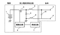
図1は、本実施形態に係る突入電流抑制回路の構成を示す回路図である。本実施形態に係る突入電流抑制回路は、直流電源1を入力として負荷に電力を出力するものであり、直流電源1(例えばバッテリ)から負荷に流れる突入電流を抑制する。突入電流抑制回路は、FET5と、第1及び第2インダクタ8と、還流ダイオード9とを主体に構成されている。
FIG. 1 is a circuit diagram showing a configuration of an inrush current suppressing circuit according to the present embodiment. The inrush current suppression circuit according to the present embodiment outputs power to a load with the DC power supply 1 as an input, and suppresses an inrush current flowing from the DC power supply 1 (for example, a battery) to the load. The inrush current suppression circuit is mainly composed of an
また、負荷は、入力キャパシタ10と、一対の出力端子3,4とを含んでおり、例えばインバータなどが該当する。
The load includes an
入力キャパシタ10は、突入電流抑制回路を介して直流電源1に接続しており、一対の出力端子3,4の入力側に位置付けられている。
The
一対の出力端子3,4は、入力キャパシタ10に並列接続されて直流電流1からの入力電流を出力する。これらの出力端子3,4の間には、負荷要素(図示しない)が接続される。一方の出力端子3は直流電源1の正極側に対応し、他方の出力端子4は直流電源1のグランド側に対応している。
The pair of output terminals 3 and 4 are connected in parallel to the
FET5は、直流電源1と接続されてオンオフ制御されるスイッチング素子である。具体的には、FET5のドレインは直流電源1の正極側に接続されており、FET5のソースは、第1インダクタ8を介して一方の出力端子3に接続されている。また、FET5のゲートは、駆動回路6に接続されている。FET5は、当該FET5のゲートにオン制御信号が入力されるとオン(導通)となり、また、FET5のゲートにオフ制御信号が入力されるとオフ(非導通)となる。なお、FET(電界効果トランジスタ)以外のスイッチング素子を用いることも可能である。
The FET 5 is a switching element that is connected to the DC power source 1 and controlled to be turned on / off. Specifically, the drain of the FET 5 is connected to the positive electrode side of the DC power supply 1, and the source of the FET 5 is connected to one output terminal 3 via the
駆動回路6は、後述する発振回路7からの高周波パルス信号に基づいてオンオフ制御信号を出力し、FET5のゲートに所定の制御電圧を印加する。発振回路7は、駆動回路6の出力制御を行うものであり、駆動回路6に対して高周波パルス信号を出力する。駆動回路6及び発振回路7を通じて、FET5のスイッチング周波数やデューティを設定することができる。
The
第1インダクタ8は、直流電源1の正極側に設けられている。具体的には、第1インダクタ8は、一方の出力端子3と入力キャパシタ10の一方の電極との接続点と、FET5のソースとの間に接続されている。また、第2インダクタ8は、直流電源1のグランド側に設けられており、入力キャパシタ10の他方の電極と他方の出力端子4との接続点と、還流ダイオード9のアノードとの間に接続されている。第1及び第2インダクタ8のインダクタンス値は同じに設定されている。
The
還流ダイオード9は、FET5と第1インダクタ8との接続点にカソードを接続している。この還流ダイオード9のアノードは、第2インダクタ8から見て、入力キャパシタ10の他方の電極と他方の出力端子4との接続点とは反対側に接続されている。
The free-
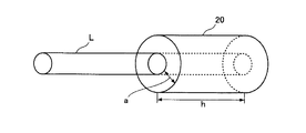
図2は、第1及び第2インダクタ8の構成を模式的に示す説明図である。本実施形態において、上記の第1及び第2インダクタ8(以下「インダクタ8」に両者を総称する)は、磁性体20から構成されている。この磁性体20は、軸方向に一定の長さを備える環状部材であり、磁性材料から成形した磁性体である。磁性体20において、環状部分の径方向長さ、すなわち電線Lが内接する内径部から外径部までの長さは「a」であり、軸方向の長さは「h」である。この磁性体20は、その内径部分に電流経路である電線Lが挿通されており、当該電線Lの回りを覆うように構成されている。
FIG. 2 is an explanatory diagram schematically showing the configuration of the first and
磁性体20として用いる磁性材料の選択は、電線Lにおける通電電流に依存する。例えば、300A位までの大電流を流す場合、パーメンジュール(permendur)や電磁軟鉄といった飽和磁束密度が大きなもの選択することが好ましい。
Selection of the magnetic material used as the
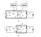
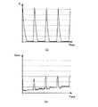
図3は、本実施形態に係る突入電流抑制回路の動作原理を模式的に示す説明図であり、(a)はFET5がオンの状態を示し、(b)はFET5がオフの状態を示す。図4は、各部の電流波形及び電圧波形の推移を示す説明図であり、(a)はインダクタ電流が不連続となる電流不連続モードを示し、(b)はインダクタ電流が連続となる電流連続モードを示している。 3A and 3B are explanatory views schematically showing the operating principle of the inrush current suppression circuit according to the present embodiment. FIG. 3A shows a state in which the FET 5 is on, and FIG. 3B shows a state in which the FET 5 is off. 4A and 4B are explanatory diagrams showing the transition of the current waveform and voltage waveform of each part, where FIG. 4A shows a current discontinuous mode in which the inductor current is discontinuous, and FIG. Indicates the mode.
FET5がオンの場合、FET5のドレイン−ソース間には、FET5のオン抵抗による電圧降下分の電圧(図4では0Vとする)が印加される。図4において、「Vds」はドレイン−ソース間の電圧である。一方、FET5がオフの場合、FET5のドレイン−ソース間には、電源電圧Vbatが印加される。
When the
FET5がオンされると、入力キャパシタ10が充電されるため、ドレイン電流Idには大電流が流れようとする。しかしながら、インダクタ8の逆起電圧により、ドレイン電流Idの増加は、図4(a)(b)に示すように、ある傾きをもって増加する。この傾きは、インダクタ8のインダクタンス値に依存する。また、電流のピーク値は、オン時間やインダクタンス値によって制御することができる。FET5がオフされると、ドレイン電流Idは流れなくなる。
When the
FET5がオンのとき、ダイオード電流Idioは流れない。一方、FET5がオフされると、インダクタ8が電流を流し続けようとするため、図3(b)に示す経路で電流が流れる。しかし、直流電源1からの電流供給がないため、この電流は、ある傾きをもって徐々に減少していく。この傾きは、インダクタ8のインダクタンス値に依存する。また、この傾きやオフ時間を変えることで、動作モードを電流連続モード(図4(a))、或いは電流不連続モード(図4(b))に切り替えることができる。
When the
FET5がオンのとき、インダクタ電流ILはドレイン電流Idが流れる。一方、FET5がオフのとき、インダクタ電流ILはダイオード電流Idioが流れる。電流不連続モードでは、入力キャパシタ10が充電されるにつれてピーク値は徐々に減少していく傾向を示す。一方、電流連続モードでは、入力キャパシタ10が充電されるにつれて、ある時間まではピーク値は増加していくが、その後減少し、入力キャパシタ10が完全に充電されると、ピーク値は一定値をとるという傾向を示す。なお、図4に示す状態は、突入電流に対応した初期的な状態を示すものであるため、上述したような傾向の全てを表しているものでない。
When the
以上の動作を入力キャパシタ10の充電完了まで繰り返すことにより、突入電流を抑制することができる。設計時には、動作周波数、デューティ比、インダクタンス値、スイッチング素子(最大定格)、ダイオード(最大定格)、プリチャージ時間などの条件により、上記の各パラメータを定めることができる。
By repeating the above operation until the charging of the
図5は、所定のパラメータが設定された突入電流抑制回路を用いた実験結果を示す説明図である。同図は、インダクタ電流ILと入力キャパシタ10の両端電圧Vconとの推移を示す説明図である。図5は、電流不連続モードにて突入電流(インダクタ電流IL)を抑制した状態を示している。なお、FET5のオン時における入力キャパシタ10の両端に加わる12乃至15V程度の電圧は、キャパシタの等価直列抵抗によるものである。
FIG. 5 is an explanatory diagram showing an experimental result using an inrush current suppression circuit in which predetermined parameters are set. This figure is an explanatory diagram showing the transition of the inductor current IL and the voltage Vcon across the
このように本実施形態において、突入電流抑制回路は、負荷に流れる突入電流を抑制するものであり、この負荷は、電源1に接続する入力キャパシタ10と、当該入力キャパシタ10に並列接続されて電源1からの入力電流を出力する一対の出力端子3,4とを備えている。ここで、突入電流抑制回路は、直流電源1と接続されてオンオフ制御されるFET5と、接続点(一方の出力端子3と入力キャパシタ10の一方の電極との接続点)とFET5との間に接続される第1インダクタ8と、FET5と第1インダクタ8との接続点にカソードを接続する還流ダイオード9と、接続点(入力キャパシタ10の他方の電極と他方の出力端子4との接続点)とダイオードのアノードとの間に接続される第2インダクタ8と、を有している。この場合、第1及び第2インダクタ8は、電流経路である電線Lの回りを覆う磁性体20から構成される。
Thus, in this embodiment, the inrush current suppression circuit suppresses inrush current flowing through the load. This load is connected in parallel to the
ここで、突入電流抑制回路について、インダクタ8がないと仮定し、FET5をオフからオンにすることを考える。突入電流抑制回路に対して直流電源1の電圧が印加されると、入力キャパシタ10を充電するため、大きな電流が短時間に流れる。この電流(突入電流)により、FET5が破壊され、遮断動作ができなくなることが問題となる。
Here, it is assumed that the inrush current suppression circuit has no
この点、本実施形態によれば、インダクタ8を設けることで、大電流が流れることが抑制することができる。これにより、FET5が破壊され、遮断動作ができなくなるといった問題を解決することができる。
In this regard, according to the present embodiment, the provision of the
また、本実施形態によれば、磁性体20をインダクタ8として利用することで、コイルのように電線を巻いてインダクタ8を形成する必要がない。そのため、大径の電線をコイルとすることによる回路の大型化を抑制することができる。また、電線を巻回する作業を省略することができるので、その製造作業の簡素化や、製造工程の短縮やコストの低減を図ることができる。
Further, according to the present embodiment, by using the
さらに、同じインダクタンス値のインダクタ8を正極側及びグランド側の両方に使うことで、回路の偏りを少なくすることにより、コモンモードノイズがノーマルモードノイズに変化することを防ぐことができるので、動作への悪影響を少なくすることができる。
Further, by using the
なお、磁性体20をインダクタ8として用いる場合、磁性体のBH曲線、周波数特性、寸法(a,h)、電線に流れる電流の値、動作周波数など、考慮しなければならない要素が多く存在する。また、電流値が一定でないことや、磁性体に幅があること等から、設計時において磁性体中の磁界を一様に決定することが難しい。そこで、磁性体20を軸方向に沿って輪切り状に分割して構成し、その分割した環状要素の個数を選択することにより軸方向の長さhを可変とすることが好ましい。これにより、製造時において軸方向の長さhを容易に変更することができるので、設計時の誤差を吸収することができる。
When the
以上、本実施形態にかかる突入電流抑制回路について説明したが、本発明はこの実施形態に限定されることなく、その発明の範囲において種々の変更が可能である。例えば「電源」は、一次電池や二次電池のように直流電流をそのまま出力するもののみならず、交流電源の出力を整流器により整流して直流電流を出力するようなものであってもよいし、交流電源そのものであってもよい。また、本実施形態では、第1及び第2インダクタのインダクタンス値は同一に設定されているが、これが厳密に一致することは要せず、各インダクタが同等の機能を果たす範囲であればその相違があってもよい。 The inrush current suppression circuit according to the present embodiment has been described above, but the present invention is not limited to this embodiment, and various modifications can be made within the scope of the present invention. For example, the “power source” is not limited to a direct current output as is the case with a primary battery or a secondary battery, but may be a type that outputs a direct current by rectifying the output of the alternating current power supply with a rectifier. The AC power supply itself may be used. In the present embodiment, the inductance values of the first and second inductors are set to be the same, but it is not necessary that they are strictly matched. There may be.
1 直流電源
3 出力端子
4 出力端子
5 FET
6 駆動回路
7 発振回路
8 インダクタ
9 ダイオード
10 キャパシタ
20 磁性体
1 DC power supply 3 Output terminal 4
6 Drive
Claims (2)
前記電源と接続されてオンオフ制御されるスイッチング素子と、
一方の出力端子と前記入力キャパシタの一方の電極との接続点と、前記スイッチング素子との間に接続される第1インダクタと、
前記スイッチング素子と前記第1インダクタとの接続点にカソードを接続するダイオードと、
前記入力キャパシタの他方の電極と他方の出力端子との接続点と、前記ダイオードのアノードとの間に接続される第2インダクタと、を有し、
前記第1インダクタ及び前記第2インダクタは、軸方向に沿って所定の長さを有する環状の磁性体にて、電流経路である電線の周りを覆って構成されることを特徴とする突入電流抑制回路。 In an inrush current suppression circuit for suppressing an inrush current flowing in a load including an input capacitor connected to a power supply and a pair of output terminals connected in parallel to the input capacitor and outputting an input current from the power supply,
A switching element connected to the power source and controlled to be turned on / off;
A first inductor connected between a connection point between one output terminal and one electrode of the input capacitor and the switching element;
A diode connecting a cathode to a connection point between the switching element and the first inductor;
A second inductor connected between a connection point between the other electrode of the input capacitor and the other output terminal, and an anode of the diode;
The first inductor and the second inductor are formed of an annular magnetic body having a predetermined length along an axial direction so as to cover an electric wire which is a current path. circuit.
Priority Applications (4)
| Application Number | Priority Date | Filing Date | Title |
|---|---|---|---|
| JP2014028150A JP2015154656A (en) | 2014-02-18 | 2014-02-18 | Rush current suppression circuit |
| CN201580004825.3A CN105917540A (en) | 2014-02-18 | 2015-02-17 | Inrush current suppression circuit |
| PCT/JP2015/054346 WO2015125793A1 (en) | 2014-02-18 | 2015-02-17 | Inrush current suppression circuit |
| US15/208,817 US20160336739A1 (en) | 2014-02-18 | 2016-07-13 | Inrush current suppression circuit |
Applications Claiming Priority (1)
| Application Number | Priority Date | Filing Date | Title |
|---|---|---|---|
| JP2014028150A JP2015154656A (en) | 2014-02-18 | 2014-02-18 | Rush current suppression circuit |
Publications (2)
| Publication Number | Publication Date |
|---|---|
| JP2015154656A true JP2015154656A (en) | 2015-08-24 |
| JP2015154656A5 JP2015154656A5 (en) | 2016-07-28 |
Family
ID=53878294
Family Applications (1)
| Application Number | Title | Priority Date | Filing Date |
|---|---|---|---|
| JP2014028150A Abandoned JP2015154656A (en) | 2014-02-18 | 2014-02-18 | Rush current suppression circuit |
Country Status (4)
| Country | Link |
|---|---|
| US (1) | US20160336739A1 (en) |
| JP (1) | JP2015154656A (en) |
| CN (1) | CN105917540A (en) |
| WO (1) | WO2015125793A1 (en) |
Cited By (1)
| Publication number | Priority date | Publication date | Assignee | Title |
|---|---|---|---|---|
| JP2016144351A (en) * | 2015-02-04 | 2016-08-08 | 矢崎総業株式会社 | Rush current suppression circuit |
Families Citing this family (2)
| Publication number | Priority date | Publication date | Assignee | Title |
|---|---|---|---|---|
| CN107069688A (en) * | 2017-05-05 | 2017-08-18 | 西安太世德航空电器有限公司 | A kind of surge restraint circuit and Surge suppression method |
| CN113541457B (en) * | 2020-04-21 | 2023-04-25 | 株洲中车时代电气股份有限公司 | Pre-charging circuit and pre-charging method of converter |
Citations (6)
| Publication number | Priority date | Publication date | Assignee | Title |
|---|---|---|---|---|
| JPH02111221A (en) * | 1988-10-20 | 1990-04-24 | Oki Electric Ind Co Ltd | Dc power source |
| JPH11178342A (en) * | 1997-12-16 | 1999-07-02 | Canon Inc | Power supply unit, electronic apparatus, and step-down type rectification/smoothing circuit |
| JP2004242418A (en) * | 2003-02-05 | 2004-08-26 | Honda Motor Co Ltd | Motor drive unit |
| JP2005094980A (en) * | 2003-09-19 | 2005-04-07 | Sony Corp | Switching power supply circuit |
| JP2009247092A (en) * | 2008-03-31 | 2009-10-22 | Honda Motor Co Ltd | Dc-dc converter and fuel cell vehicle |
| JP2012090363A (en) * | 2010-10-15 | 2012-05-10 | Denso Corp | Protection device for load drive control device |
Family Cites Families (7)
| Publication number | Priority date | Publication date | Assignee | Title |
|---|---|---|---|---|
| JPH05260736A (en) * | 1992-03-13 | 1993-10-08 | Ricoh Co Ltd | Switching regulator |
| DE4310748A1 (en) * | 1993-04-01 | 1994-10-06 | Siemens Ag | Switching controller |
| JPH08275383A (en) * | 1995-03-28 | 1996-10-18 | Fukushima Nippon Denki Kk | Rush current preventive circuitry |
| JP2002095158A (en) * | 2000-09-08 | 2002-03-29 | Tokin Corp | Lightning surge suppressor |
| JP2005073335A (en) * | 2003-08-21 | 2005-03-17 | Sony Corp | Switching power supply circuit |
| US8717001B2 (en) * | 2012-07-03 | 2014-05-06 | Infineon Technologies Austria Ag | Inrush current limiting circuit |
| CN203251084U (en) * | 2013-05-28 | 2013-10-23 | 北京联动天翼科技有限公司 | Bi-directional current limiter based on bi-directional BUCK converter |
-
2014
- 2014-02-18 JP JP2014028150A patent/JP2015154656A/en not_active Abandoned
-
2015
- 2015-02-17 WO PCT/JP2015/054346 patent/WO2015125793A1/en active Application Filing
- 2015-02-17 CN CN201580004825.3A patent/CN105917540A/en active Pending
-
2016
- 2016-07-13 US US15/208,817 patent/US20160336739A1/en not_active Abandoned
Patent Citations (6)
| Publication number | Priority date | Publication date | Assignee | Title |
|---|---|---|---|---|
| JPH02111221A (en) * | 1988-10-20 | 1990-04-24 | Oki Electric Ind Co Ltd | Dc power source |
| JPH11178342A (en) * | 1997-12-16 | 1999-07-02 | Canon Inc | Power supply unit, electronic apparatus, and step-down type rectification/smoothing circuit |
| JP2004242418A (en) * | 2003-02-05 | 2004-08-26 | Honda Motor Co Ltd | Motor drive unit |
| JP2005094980A (en) * | 2003-09-19 | 2005-04-07 | Sony Corp | Switching power supply circuit |
| JP2009247092A (en) * | 2008-03-31 | 2009-10-22 | Honda Motor Co Ltd | Dc-dc converter and fuel cell vehicle |
| JP2012090363A (en) * | 2010-10-15 | 2012-05-10 | Denso Corp | Protection device for load drive control device |
Cited By (2)
| Publication number | Priority date | Publication date | Assignee | Title |
|---|---|---|---|---|
| JP2016144351A (en) * | 2015-02-04 | 2016-08-08 | 矢崎総業株式会社 | Rush current suppression circuit |
| US10128651B2 (en) | 2015-02-04 | 2018-11-13 | Yazaki Corporation | Inrush current inhibiting circuit including a control part that controls a switching element |
Also Published As
| Publication number | Publication date |
|---|---|
| CN105917540A (en) | 2016-08-31 |
| US20160336739A1 (en) | 2016-11-17 |
| WO2015125793A1 (en) | 2015-08-27 |
Similar Documents
| Publication | Publication Date | Title |
|---|---|---|
| JP6291432B2 (en) | Inrush current suppression circuit | |
| JP5759482B2 (en) | Power conversion by zero voltage switching | |
| JP5830915B2 (en) | Power conversion circuit | |
| US11018592B2 (en) | Flyback converter controller, flyback converter and methods of operation | |
| JP6099581B2 (en) | Switching power supply | |
| JP4175367B2 (en) | Switching power supply | |
| WO2015125793A1 (en) | Inrush current suppression circuit | |
| JP2019041531A (en) | LLC resonant converter | |
| JP6350753B2 (en) | Power circuit | |
| US7977920B2 (en) | Voltage-converter circuit and method for clocked supply of energy to an energy storage | |
| JP4434011B2 (en) | DC converter | |
| JP5959459B2 (en) | DC-DC converter | |
| TWI586092B (en) | Single-stage ac-to-dc converter | |
| JP5597276B1 (en) | Power supply | |
| JP2007181375A (en) | High-voltage pulse generation circuit and pulse width changing method | |
| JP5954256B2 (en) | Control method | |
| JP6091324B2 (en) | DC power supply | |
| JPWO2011074154A1 (en) | DC / DC converter | |
| JP6711150B2 (en) | Boost circuit | |
| RU2667896C2 (en) | Switched-mode converter and method for converting electrical energy | |
| JP2020202645A (en) | Converter and control method thereof | |
| JP7347010B2 (en) | Buck-boost chopper circuit and DC power supply | |
| JP2018153037A (en) | Dc conversion device | |
| JP2012178952A (en) | Switching power supply circuit | |
| JP2009207272A (en) | Dc booster circuit |
Legal Events
| Date | Code | Title | Description |
|---|---|---|---|
| A521 | Request for written amendment filed |
Free format text: JAPANESE INTERMEDIATE CODE: A523 Effective date: 20160609 |
|
| A621 | Written request for application examination |
Free format text: JAPANESE INTERMEDIATE CODE: A621 Effective date: 20170119 |
|
| A131 | Notification of reasons for refusal |
Free format text: JAPANESE INTERMEDIATE CODE: A131 Effective date: 20170711 |
|
| A762 | Written abandonment of application |
Free format text: JAPANESE INTERMEDIATE CODE: A762 Effective date: 20170913 |