JP2015114308A - Tactile sensor - Google Patents
Tactile sensor Download PDFInfo
- Publication number
- JP2015114308A JP2015114308A JP2013259114A JP2013259114A JP2015114308A JP 2015114308 A JP2015114308 A JP 2015114308A JP 2013259114 A JP2013259114 A JP 2013259114A JP 2013259114 A JP2013259114 A JP 2013259114A JP 2015114308 A JP2015114308 A JP 2015114308A
- Authority
- JP
- Japan
- Prior art keywords
- row
- column
- electrode layer
- individual
- layer
- Prior art date
- Legal status (The legal status is an assumption and is not a legal conclusion. Google has not performed a legal analysis and makes no representation as to the accuracy of the status listed.)
- Granted
Links
- 238000001514 detection method Methods 0.000 claims abstract description 420
- 230000005489 elastic deformation Effects 0.000 claims abstract description 84
- 239000011159 matrix material Substances 0.000 claims abstract description 83
- 238000005520 cutting process Methods 0.000 claims description 37
- 230000006870 function Effects 0.000 claims description 35
- 239000000463 material Substances 0.000 claims description 31
- 239000004020 conductor Substances 0.000 claims description 30
- 229920001971 elastomer Polymers 0.000 claims description 23
- 125000006850 spacer group Chemical group 0.000 claims description 19
- 239000002184 metal Substances 0.000 claims description 12
- 229910052751 metal Inorganic materials 0.000 claims description 12
- OKTJSMMVPCPJKN-UHFFFAOYSA-N Carbon Chemical compound [C] OKTJSMMVPCPJKN-UHFFFAOYSA-N 0.000 claims description 7
- 229910052799 carbon Inorganic materials 0.000 claims description 7
- 230000002093 peripheral effect Effects 0.000 claims description 7
- 238000010030 laminating Methods 0.000 claims description 6
- 230000035807 sensation Effects 0.000 claims description 2
- 230000003247 decreasing effect Effects 0.000 claims 4
- 238000003825 pressing Methods 0.000 abstract description 21
- 238000012986 modification Methods 0.000 description 29
- 230000004048 modification Effects 0.000 description 29
- 238000010586 diagram Methods 0.000 description 13
- 230000007423 decrease Effects 0.000 description 10
- 238000005452 bending Methods 0.000 description 8
- 230000012447 hatching Effects 0.000 description 8
- 239000000758 substrate Substances 0.000 description 6
- 239000004642 Polyimide Substances 0.000 description 5
- 229920001721 polyimide Polymers 0.000 description 5
- RYGMFSIKBFXOCR-UHFFFAOYSA-N Copper Chemical compound [Cu] RYGMFSIKBFXOCR-UHFFFAOYSA-N 0.000 description 4
- 239000011889 copper foil Substances 0.000 description 4
- 238000003475 lamination Methods 0.000 description 4
- 238000000034 method Methods 0.000 description 4
- 238000006073 displacement reaction Methods 0.000 description 3
- 238000005259 measurement Methods 0.000 description 3
- 229920005989 resin Polymers 0.000 description 3
- 239000011347 resin Substances 0.000 description 3
- 229920002379 silicone rubber Polymers 0.000 description 3
- 239000004945 silicone rubber Substances 0.000 description 3
- 239000004593 Epoxy Substances 0.000 description 2
- 239000000654 additive Substances 0.000 description 2
- 230000000996 additive effect Effects 0.000 description 2
- 239000000919 ceramic Substances 0.000 description 2
- 239000000470 constituent Substances 0.000 description 2
- 239000011888 foil Substances 0.000 description 2
- 239000011521 glass Substances 0.000 description 2
- 229920006254 polymer film Polymers 0.000 description 2
- 238000007639 printing Methods 0.000 description 2
- 238000012545 processing Methods 0.000 description 2
- 238000009751 slip forming Methods 0.000 description 2
- 239000002759 woven fabric Substances 0.000 description 2
- 238000006243 chemical reaction Methods 0.000 description 1
- 238000011161 development Methods 0.000 description 1
- 230000018109 developmental process Effects 0.000 description 1
- 230000000694 effects Effects 0.000 description 1
- 239000013013 elastic material Substances 0.000 description 1
- 238000005516 engineering process Methods 0.000 description 1
- 239000004744 fabric Substances 0.000 description 1
- 230000008570 general process Effects 0.000 description 1
- 238000005304 joining Methods 0.000 description 1
- 238000004519 manufacturing process Methods 0.000 description 1
- 230000000474 nursing effect Effects 0.000 description 1
- 230000003287 optical effect Effects 0.000 description 1
- 239000013307 optical fiber Substances 0.000 description 1
- 230000036544 posture Effects 0.000 description 1
- 230000008569 process Effects 0.000 description 1
- 238000004088 simulation Methods 0.000 description 1
- 238000011895 specific detection Methods 0.000 description 1
- 230000002195 synergetic effect Effects 0.000 description 1
Images


Landscapes
- Force Measurement Appropriate To Specific Purposes (AREA)
Abstract
Description
本発明は、触覚センサに関し、特に、産業機器やロボットなどに取り付け、物体との接触圧を測定するのに適した触覚センサに関する。 The present invention relates to a tactile sensor, and more particularly, to a tactile sensor that is attached to an industrial device or a robot and is suitable for measuring a contact pressure with an object.
触覚センサは、産業機器やロボットなどのハンド部に加わる接触圧を検出するセンサとして広く利用されている。また、二次元平面上の個々の位置に加わる接触圧を独立して検出する機能をもった触覚センサは、いわゆるタッチパネルとして、様々な電子機器用の入力装置としても用いられている。触覚センサに用いる接触圧の検出原理としては、その形態や用途に応じて、静電容量式、感圧抵抗式、コイル式、光学式など、様々な形式が提案されている。 A tactile sensor is widely used as a sensor for detecting a contact pressure applied to a hand unit of an industrial device or a robot. A tactile sensor having a function of independently detecting a contact pressure applied to each position on a two-dimensional plane is also used as an input device for various electronic devices as a so-called touch panel. As the detection principle of the contact pressure used in the tactile sensor, various types such as a capacitance type, a pressure sensitive resistance type, a coil type, and an optical type have been proposed depending on the form and application.
たとえば、下記の特許文献1には、静電容量式のタッチパネルが開示され、特許文献2には、感圧抵抗式のタッチパネルが開示されている。また、特許文献3には、二次元平面上に多数のコイルを配置した触覚センサが開示され、特許文献4には、光ファイバを用いて光学的に剪断応力の検出を行う触覚センサが開示されている。更に、特許文献5には、二次元平面上に配列された多数の接触子の変位を感圧センサで検出する触覚センサが開示され、特許文献6には、押圧により抵抗値が変化するシート状の感圧導電性部材をマトリクス状に配列した触覚センサが開示されている。 For example, the following Patent Document 1 discloses a capacitive touch panel, and Patent Document 2 discloses a pressure-sensitive resistance touch panel. Patent Document 3 discloses a tactile sensor in which a large number of coils are arranged on a two-dimensional plane, and Patent Document 4 discloses a tactile sensor that optically detects shear stress using an optical fiber. ing. Further, Patent Document 5 discloses a tactile sensor that detects a displacement of a large number of contacts arranged on a two-dimensional plane with a pressure-sensitive sensor, and Patent Document 6 discloses a sheet-like shape whose resistance value changes due to pressing. A tactile sensor in which the pressure-sensitive conductive members are arranged in a matrix is disclosed.
一方、ロボットのアーム部などの曲面に合わせた実装が可能になる工夫として、特許文献7には、多数の感圧素子をフレキシブル基板上に配列して構成される柔軟触覚センサが開示されており、特許文献8には、高分子フィルム上に金属層および抵抗体を形成した曲面付着型触覚センサが開示されている。 On the other hand, Patent Document 7 discloses a flexible tactile sensor configured by arranging a large number of pressure-sensitive elements on a flexible substrate as a device that enables mounting in accordance with the curved surface of a robot arm or the like. Patent Document 8 discloses a curved surface adhesion type tactile sensor in which a metal layer and a resistor are formed on a polymer film.
近年、コンピュータによる制御技術の発展とともに、人型ロボットが脚光を浴びている。将来は、産業界のみならず一般家庭においても、介護や家事などを行う人型ロボットが普及するものと期待される。このような人型ロボットでは、指先の動きを正確に制御することにより、人間と同様、きめ細かな動作を行わせることが可能になるが、そのためには、1本1本の指先に装着する触覚センサが必要になる。 In recent years, with the development of computer control technology, humanoid robots have attracted attention. In the future, it is expected that humanoid robots for nursing care and housework will become popular not only in industry but also in general households. In such a humanoid robot, by precisely controlling the movement of the fingertip, it becomes possible to perform a fine operation like a human being. For this purpose, a tactile sensation attached to each fingertip is required. A sensor is required.
ところが、人型ロボットの指は、人間の指に似せて作られているため、指先の形状も単純な平面や円筒形ではなく、球状に近い任意形状をしている。このため、従来提案されている一般的な触覚センサは、人型ロボットの指先のような任意形状面に装着するのには不適当である。 However, since the finger of the humanoid robot is made to resemble a human finger, the shape of the fingertip is not a simple plane or cylinder, but an arbitrary shape close to a sphere. For this reason, the conventionally proposed general tactile sensor is not suitable for mounting on an arbitrary shape surface such as a fingertip of a humanoid robot.
もちろん、前掲の特許文献7,8には、フレキシブル基板や高分子フィルムを利用することにより、曲面に装着可能な柔軟なシート状の触覚センサが提案されている。しかしながら、このようなシート状の触覚センサは、ロボットのアーム部など、円筒状部分の表面に装着するのには適しているが、人型ロボットの指先のように、球面に近い曲面に装着することは困難である。 Of course, Patent Documents 7 and 8 cited above propose a flexible sheet-like tactile sensor that can be mounted on a curved surface by using a flexible substrate or a polymer film. However, such a sheet-like tactile sensor is suitable for mounting on the surface of a cylindrical portion such as a robot arm, but it is mounted on a curved surface close to a spherical surface like a fingertip of a humanoid robot. It is difficult.
そこで本発明は、人型ロボットの指先のように、球面に近い曲面に装着することが可能な触覚センサを提供することを目的とする。 Accordingly, an object of the present invention is to provide a tactile sensor that can be mounted on a curved surface close to a spherical surface, such as a fingertip of a humanoid robot.
(1) 本発明の第1の態様は、m行n列の行列を構成する位置に配置されたm×n個の検出点に作用した個々の外力を検出する触覚センサにおいて、
各検出点の位置に配置され、作用した外力に基づいてその電気的特性に変化が生じるm×n個の検出素子と、
行方向に隣接する各検出素子対を相互に接続する行方向接続部と、列方向に隣接する各検出素子対を相互に接続する列方向接続部と、
を有する網状本体部と、
各検出素子に生じた電気的特性の変化に基づいて、当該検出素子が配置されている検出点に作用した外力を検出する検出回路と、
を設け、
行方向接続部および列方向接続部に可撓性をもたせ、行方向もしくは列方向に隣接する任意の検出素子対について、両者の三次元空間上での相互位置関係が、三次元の自由度をもって変化できるように構成したものである。
(1) A first aspect of the present invention is a tactile sensor that detects individual external forces acting on m × n detection points arranged at positions constituting a matrix of m rows and n columns.
M × n detection elements that are arranged at the positions of the respective detection points and change in their electrical characteristics based on the applied external force;
A row-direction connecting portion for mutually connecting each detecting element pair adjacent in the row direction, and a column-direction connecting portion for connecting each detecting element pair adjacent in the column direction to each other;
A net-like body having
A detection circuit for detecting an external force applied to a detection point where the detection element is arranged based on a change in electrical characteristics generated in each detection element;
Provided,
The row direction connection part and the column direction connection part are made flexible, and the mutual positional relationship in the three-dimensional space of any detector element pair adjacent in the row direction or the column direction has a three-dimensional degree of freedom. It is configured so that it can change.
(2) 本発明の第2の態様は、上述した第1の態様に係る触覚センサにおいて、
各検出素子が、上方に配置された上部個別電極層と、この上部個別電極層に対向するように下方に配置された下部個別電極層と、これら一対の個別電極層間に介挿された中間要素と、を有し、
中間要素は、一対の個別電極層間の間隔を縮める方向に外力が作用すると、少なくともその一部が弾性変形を生じ、外力が作用しなくなったときに当該間隔を元に復元させる性質をもち、かつ、当該間隔の変化に応じて一対の個別電極層間の電気抵抗を変化させる性質をもち、
検出回路が、上記電気抵抗に基づいて、作用した外力を検出するようにしたものである。
(2) A second aspect of the present invention is the tactile sensor according to the first aspect described above,
Each detection element includes an upper individual electrode layer disposed above, a lower individual electrode layer disposed below to face the upper individual electrode layer, and an intermediate element interposed between the pair of individual electrode layers. And having
The intermediate element has a property that when an external force acts in a direction to reduce the distance between the pair of individual electrode layers, at least a part thereof is elastically deformed, and when the external force stops working, the intermediate element is restored based on the distance. , Having the property of changing the electrical resistance between the pair of individual electrode layers according to the change in the interval,
The detection circuit detects the applied external force based on the electric resistance.
(3) 本発明の第3の態様は、上述した第2の態様に係る触覚センサにおいて、
中間要素が、上部個別電極層の下面から下方に凸となるように隆起した形状をなす個別弾性変形体と、下部個別電極層の上面に形成された個別抵抗体層と、を有し、
個別弾性変形体は導電体もしくは抵抗体から構成されており、その上面は上部個別電極層の下面に接続され、その下端は個別抵抗体層の上面に接触しており、
一対の個別電極層間の間隔を縮める方向に外力が作用すると、個別弾性変形体が弾性変形を生じて当該間隔が縮み、個別弾性変形体と個別抵抗体層の上面との接触面積が増加することにより、一対の個別電極層間の電気抵抗が減少するようにしたものである。
(3) A third aspect of the present invention is the tactile sensor according to the second aspect described above,
The intermediate element has an individual elastic deformation body having a shape protruding so as to protrude downward from the lower surface of the upper individual electrode layer, and an individual resistor layer formed on the upper surface of the lower individual electrode layer,
The individual elastic deformation body is composed of a conductor or a resistor, the upper surface thereof is connected to the lower surface of the upper individual electrode layer, and the lower end thereof is in contact with the upper surface of the individual resistor layer,
When an external force acts in a direction to reduce the distance between the pair of individual electrode layers, the individual elastic deformable body is elastically deformed, the distance is reduced, and the contact area between the individual elastic deformable body and the upper surface of the individual resistor layer is increased. Thus, the electrical resistance between the pair of individual electrode layers is reduced.
(4) 本発明の第4の態様は、上述した第2の態様に係る触覚センサにおいて、
中間要素が、上部個別電極層の下面から下方に凸となるように隆起した形状をなす個別弾性変形体を有し、
個別弾性変形体は抵抗体から構成されており、その上面は上部個別電極層の下面に接続され、その下端は下部個別電極層の上面に接触しており、
一対の個別電極層間の間隔を縮める方向に外力が作用すると、個別弾性変形体が弾性変形を生じて当該間隔が縮み、個別弾性変形体と下部個別電極層の上面との接触面積が増加することにより、一対の個別電極層間の電気抵抗が減少するようにしたものである。
(4) A fourth aspect of the present invention is the tactile sensor according to the second aspect described above,
The intermediate element has an individual elastic deformation body having a shape protruding so as to protrude downward from the lower surface of the upper individual electrode layer,
The individual elastic deformation body is composed of a resistor, its upper surface is connected to the lower surface of the upper individual electrode layer, and its lower end is in contact with the upper surface of the lower individual electrode layer,
When an external force acts in a direction to reduce the distance between the pair of individual electrode layers, the individual elastic deformable body is elastically deformed, the distance is reduced, and the contact area between the individual elastic deformable body and the upper surface of the lower individual electrode layer is increased. Thus, the electrical resistance between the pair of individual electrode layers is reduced.
(5) 本発明の第5の態様は、上述した第2の態様に係る触覚センサにおいて、
中間要素が、上面が上部個別電極層の下面に接続され、下面が凹凸構造面を有する個別弾性変形体と、下部個別電極層の上面に形成された個別抵抗体層と、を有し、
個別弾性変形体は導電体もしくは抵抗体から構成されており、凹凸構造面は個別抵抗体層の上面に接触しており、
一対の個別電極層間の間隔を縮める方向に外力が作用すると、個別弾性変形体が弾性変形を生じて当該間隔が縮み、個別弾性変形体と個別抵抗体層の上面との接触面積が増加することにより、一対の個別電極層間の電気抵抗が減少するようにしたものである。
(5) A fifth aspect of the present invention is the tactile sensor according to the second aspect described above,
The intermediate element has an individual elastic deformation body whose upper surface is connected to the lower surface of the upper individual electrode layer and whose lower surface has an uneven structure surface, and an individual resistor layer formed on the upper surface of the lower individual electrode layer,
The individual elastic deformation body is composed of a conductor or a resistor, and the concavo-convex structure surface is in contact with the upper surface of the individual resistor layer.
When an external force acts in a direction to reduce the distance between the pair of individual electrode layers, the individual elastic deformable body is elastically deformed, the distance is reduced, and the contact area between the individual elastic deformable body and the upper surface of the individual resistor layer is increased. Thus, the electrical resistance between the pair of individual electrode layers is reduced.
(6) 本発明の第6の態様は、上述した第2の態様に係る触覚センサにおいて、
中間要素が、上面が上部個別電極層の下面に接続され、下面が凹凸構造面を有する個別弾性変形体を有し、個別弾性変形体は抵抗体から構成されており、凹凸構造面は下部個別電極層の上面に接触しており、
一対の個別電極層間の間隔を縮める方向に外力が作用すると、個別弾性変形体が弾性変形を生じて当該間隔が縮み、個別弾性変形体と下部個別電極層の上面との接触面積が増加することにより、一対の個別電極層間の電気抵抗が減少するようにしたものである。
(6) A sixth aspect of the present invention is the tactile sensor according to the second aspect described above,
The intermediate element has an individual elastic deformation body whose upper surface is connected to the lower surface of the upper individual electrode layer and whose lower surface has an uneven structure surface, and the individual elastic deformation body is composed of a resistor, and the uneven structure surface is an individual lower surface In contact with the upper surface of the electrode layer,
When an external force acts in a direction to reduce the distance between the pair of individual electrode layers, the individual elastic deformable body is elastically deformed, the distance is reduced, and the contact area between the individual elastic deformable body and the upper surface of the lower individual electrode layer is increased. Thus, the electrical resistance between the pair of individual electrode layers is reduced.
(7) 本発明の第7の態様は、上述した第3〜第6の態様に係る触覚センサにおいて、
m行n列の行列状に配置された各検出素子のうち、第i行目(i=1〜m)に配列されたn個の検出素子の上部個別電極層は相互に電気的に接続され、第i番目の行方向導電路を形成し、第j列目(j=1〜n)に配列されたm個の検出素子の下部個別電極層は相互に電気的に接続され、第j番目の列方向導電路を形成し、
検出回路が、第i番目の行方向導電路と第j番目の列方向導電路との間の電気抵抗に基づいて、第i行第j列目(i=1〜m,j=1〜n)に配置された検出点に作用した外力を検出するようにしたものである。
(7) A seventh aspect of the present invention is the tactile sensor according to the third to sixth aspects described above,
Of the detection elements arranged in a matrix of m rows and n columns, the upper individual electrode layers of the n detection elements arranged in the i-th row (i = 1 to m) are electrically connected to each other. The lower individual electrode layers of the m detection elements arranged in the j-th column (j = 1 to n) forming the i-th row-direction conductive path are electrically connected to each other, and the j-th Forming a column-direction conductive path of
Based on the electrical resistance between the i-th row-direction conductive path and the j-th column-direction conductive path, the detection circuit detects the i-th row and j-th column (i = 1 to m, j = 1 to n). ) To detect an external force acting on the detection point arranged in (1).
(8) 本発明の第8の態様は、上述した第1〜第7の態様に係る触覚センサにおいて、
行方向接続部および列方向接続部が、クランク状もしくはS字状の屈曲構造を有するようにしたものである。
(8) The eighth aspect of the present invention is the tactile sensor according to the first to seventh aspects described above,
The row direction connecting portion and the column direction connecting portion have a crank-shaped or S-shaped bent structure.
(9) 本発明の第9の態様は、m行n列の行列を構成する位置に配置されたm×n個の検出点に作用した個々の外力を検出する触覚センサにおいて、
上部網状部材と、下部網状部材と、検出回路と、を設け、
上部網状部材は、上部支持層と、上部支持層の下面に形成された上部電極層と、上部電極層の下面に形成された変形体層と、を有し、
下部網状部材は、下部支持層と、下部支持層の上面に形成された下部電極層と、下部電極層の上面に形成された抵抗体層と、を有し、
上部支持層は、m行n列の行列を構成するように配置されたm×n個の上部検出素片と、第i行目(i=1〜m)に配列されたn個の上部検出素片のうち、それぞれ隣接する一対の上部検出素片を相互に接続する可撓性をもった上部行方向接続部と、第j列目(j=1〜n)に配列されたm個の上部検出素片のうち、それぞれ隣接する一対の上部検出素片を相互に接続する可撓性をもった上部列方向接続部と、を有し、
上部電極層は、各上部検出素片の下面に形成されたm×n個の上部個別電極層と、各上部行方向接続部の下面に形成された上部行方向接続電極層と、を有し、第i行目に配列された上部個別電極層および第i行目に配列された上部行方向接続電極層は相互に電気的に接続され、第i番目の行方向導電路を形成し、
変形体層は、各上部個別電極層の下面から下方に凸となるように隆起した形状をなすm×n個の個別弾性変形体を有し、各個別弾性変形体は導電体もしくは抵抗体から構成されており、その上面はそれぞれ上方に位置する個々の上部個別電極層の下面に接続され、
下部支持層は、m行n列の行列を構成するように配置されたm×n個の下部検出素片と、第i行目(i=1〜m)に配列されたn個の下部検出素片のうち、それぞれ隣接する一対の下部検出素片を相互に接続する可撓性をもった下部行方向接続部と、第j列目(j=1〜n)に配列されたm個の下部検出素片のうち、それぞれ隣接する一対の下部検出素片を相互に接続する可撓性をもった下部列方向接続部と、を有し、
下部電極層は、各下部検出素片の上面に形成されたm×n個の下部個別電極層と、各下部列方向接続部の上面に形成された下部列方向接続電極層と、を有し、第j列目に配列された下部個別電極層および第j列目に配列された下部列方向接続電極層は相互に電気的に接続され、第j番目の列方向導電路を形成し、
抵抗体層は、各下部個別電極層の上面に形成されたm×n個の個別抵抗体層を有し、
上部網状部材は、第i行第j列目(i=1〜m,j=1〜n)に配置された個別弾性変形体の下端が、第i行第j列目に配置された個別抵抗体層の上面に接触するように、下部網状部材の上方に積層配置されており、
検出回路は、第i番目の行方向導電路と第j番目の列方向導電路との間の電気抵抗に基づいて、第i行第j列目(i=1〜m,j=1〜n)に配置された検出点に作用した外力を検出するようにしたものである。
(9) A ninth aspect of the present invention is a tactile sensor for detecting individual external forces acting on m × n detection points arranged at positions constituting an m × n matrix,
An upper mesh member, a lower mesh member, and a detection circuit;
The upper mesh member has an upper support layer, an upper electrode layer formed on the lower surface of the upper support layer, and a deformable body layer formed on the lower surface of the upper electrode layer,
The lower mesh member has a lower support layer, a lower electrode layer formed on the upper surface of the lower support layer, and a resistor layer formed on the upper surface of the lower electrode layer,
The upper support layer includes m × n upper detection elements arranged to form an m × n matrix, and n upper detection elements arranged in the i th row (i = 1 to m). Among the segments, a flexible upper row direction connecting portion for mutually connecting a pair of adjacent upper detection segments, and m pieces arranged in the j-th column (j = 1 to n) A flexible upper row-direction connecting portion for mutually connecting a pair of upper detection pieces adjacent to each other among the upper detection pieces;
The upper electrode layer has m × n upper individual electrode layers formed on the lower surface of each upper detection element, and upper row direction connection electrode layers formed on the lower surface of each upper row connection portion. The upper individual electrode layer arranged in the i-th row and the upper row-direction connection electrode layer arranged in the i-th row are electrically connected to each other to form an i-th row-direction conductive path,
The deformable body layer has m × n individual elastic deformable bodies having a shape that protrudes downward from the lower surface of each upper individual electrode layer, and each individual elastic deformable body is formed of a conductor or a resistor. Each of the upper surfaces thereof is connected to the lower surfaces of the individual upper individual electrode layers located above,
The lower support layer includes m × n lower detection elements arranged to form an m × n matrix, and n lower detections arranged in the i th row (i = 1 to m). Among the segments, a flexible lower row-direction connecting portion that connects a pair of adjacent lower detection segments to each other, and m pieces arranged in the j-th column (j = 1 to n) A lower row-direction connecting portion having flexibility to mutually connect a pair of lower detection pieces adjacent to each other among the lower detection pieces;
The lower electrode layer has m × n lower individual electrode layers formed on the upper surface of each lower detection element, and a lower column direction connection electrode layer formed on the upper surface of each lower column direction connection portion. The lower individual electrode layer arranged in the j-th column and the lower column-direction connection electrode layer arranged in the j-th column are electrically connected to each other to form a j-th column-direction conductive path,
The resistor layer has m × n individual resistor layers formed on the upper surface of each lower individual electrode layer,
The upper mesh member is an individual resistor in which the lower end of the individual elastic deformation body arranged in the i-th row and j-th column (i = 1 to m, j = 1 to n) is arranged in the i-th row and j-th column. Laminated above the lower mesh member so as to contact the upper surface of the body layer,
Based on the electrical resistance between the i-th row-direction conductive path and the j-th column-direction conductive path, the detection circuit performs the i-th row and j-th column (i = 1 to m, j = 1 to n). ) To detect an external force acting on the detection point arranged in (1).
(10) 本発明の第10の態様は、m行n列の行列を構成する位置に配置されたm×n個の検出点に作用した個々の外力を検出する触覚センサにおいて、
上部網状部材と、下部網状部材と、検出回路と、を設け、
上部網状部材は、上部支持層と、上部支持層の下面に形成された上部電極層と、上部電極層の下面に形成された変形体層と、を有し、
下部網状部材は、下部支持層と、下部支持層の上面に形成された下部電極層と、を有し、
上部支持層は、m行n列の行列を構成するように配置されたm×n個の上部検出素片と、第i行目(i=1〜m)に配列されたn個の上部検出素片のうち、それぞれ隣接する一対の上部検出素片を相互に接続する可撓性をもった上部行方向接続部と、第j列目(j=1〜n)に配列されたm個の上部検出素片のうち、それぞれ隣接する一対の上部検出素片を相互に接続する可撓性をもった上部列方向接続部と、を有し、
上部電極層は、各上部検出素片の下面に形成されたm×n個の上部個別電極層と、各上部行方向接続部の下面に形成された上部行方向接続電極層と、を有し、第i行目に配列された上部個別電極層および第i行目に配列された上部行方向接続電極層は相互に電気的に接続され、第i番目の行方向導電路を形成し、
変形体層は、各上部個別電極層の下面から下方に凸となるように隆起した形状をなすm×n個の個別弾性変形体を有し、各個別弾性変形体は抵抗体から構成されており、その上面はそれぞれ上方に位置する個々の上部個別電極層の下面に接続され、
下部支持層は、m行n列の行列を構成するように配置されたm×n個の下部検出素片と、第i行目(i=1〜m)に配列されたn個の下部検出素片のうち、それぞれ隣接する一対の下部検出素片を相互に接続する可撓性をもった下部行方向接続部と、第j列目(j=1〜n)に配列されたm個の下部検出素片のうち、それぞれ隣接する一対の下部検出素片を相互に接続する可撓性をもった下部列方向接続部と、を有し、
下部電極層は、各下部検出素片の上面に形成されたm×n個の下部個別電極層と、各下部列方向接続部の上面に形成された下部列方向接続電極層と、を有し、第j列目に配列された下部個別電極層および第j列目に配列された下部列方向接続電極層は相互に電気的に接続され、第j番目の列方向導電路を形成し、
上部網状部材は、第i行第j列目(i=1〜m,j=1〜n)に配置された個別弾性変形体の下端が、第i行第j列目に配置された下部個別電極層の上面に接触するように、下部網状部材の上方に積層配置されており、
検出回路は、第i番目の行方向導電路と第j番目の列方向導電路との間の電気抵抗に基づいて、第i行第j列目(i=1〜m,j=1〜n)に配置された検出点に作用した外力を検出するようにしたものである。
(10) A tenth aspect of the present invention is a tactile sensor for detecting individual external forces acting on m × n detection points arranged at positions constituting an m × n matrix,
An upper mesh member, a lower mesh member, and a detection circuit;
The upper mesh member has an upper support layer, an upper electrode layer formed on the lower surface of the upper support layer, and a deformable body layer formed on the lower surface of the upper electrode layer,
The lower mesh member has a lower support layer, and a lower electrode layer formed on the upper surface of the lower support layer,
The upper support layer includes m × n upper detection elements arranged to form an m × n matrix, and n upper detection elements arranged in the i th row (i = 1 to m). Among the segments, a flexible upper row direction connecting portion for mutually connecting a pair of adjacent upper detection segments, and m pieces arranged in the j-th column (j = 1 to n) A flexible upper row-direction connecting portion for mutually connecting a pair of upper detection pieces adjacent to each other among the upper detection pieces;
The upper electrode layer has m × n upper individual electrode layers formed on the lower surface of each upper detection element, and upper row direction connection electrode layers formed on the lower surface of each upper row connection portion. The upper individual electrode layer arranged in the i-th row and the upper row-direction connection electrode layer arranged in the i-th row are electrically connected to each other to form an i-th row-direction conductive path,
The deformable body layer has m × n individual elastic deformable bodies having a shape protruding so as to protrude downward from the lower surface of each upper individual electrode layer, and each individual elastic deformable body is configured by a resistor. And the upper surface is connected to the lower surface of each upper individual electrode layer located above,
The lower support layer includes m × n lower detection elements arranged to form an m × n matrix, and n lower detections arranged in the i th row (i = 1 to m). Among the segments, a flexible lower row-direction connecting portion that connects a pair of adjacent lower detection segments to each other, and m pieces arranged in the j-th column (j = 1 to n) A lower row-direction connecting portion having flexibility to mutually connect a pair of lower detection pieces adjacent to each other among the lower detection pieces;
The lower electrode layer has m × n lower individual electrode layers formed on the upper surface of each lower detection element, and a lower column direction connection electrode layer formed on the upper surface of each lower column direction connection portion. The lower individual electrode layer arranged in the j-th column and the lower column-direction connection electrode layer arranged in the j-th column are electrically connected to each other to form a j-th column-direction conductive path,
The upper mesh member is a lower individual member in which the lower ends of the individual elastic deformation members arranged in the i-th row and j-th column (i = 1 to m, j = 1 to n) are arranged in the i-th row and j-th column. Laminated above the lower mesh member so as to contact the upper surface of the electrode layer,
Based on the electrical resistance between the i-th row-direction conductive path and the j-th column-direction conductive path, the detection circuit performs the i-th row and j-th column (i = 1 to m, j = 1 to n). ) To detect an external force acting on the detection point arranged in (1).
(11) 本発明の第11の態様は、m行n列の行列を構成する位置に配置されたm×n個の検出点に作用した個々の外力を検出する触覚センサにおいて、
上部網状部材と、下部網状部材と、検出回路と、を設け、
上部網状部材は、上部支持層と、上部支持層の下面に形成された上部電極層と、上部電極層の下面に形成された変形体層と、を有し、
下部網状部材は、下部支持層と、下部支持層の上面に形成された下部電極層と、下部電極層の上面に形成された抵抗体層と、を有し、
上部支持層は、m行n列の行列を構成するように配置されたm×n個の上部検出素片と、第i行目(i=1〜m)に配列されたn個の上部検出素片のうち、それぞれ隣接する一対の上部検出素片を相互に接続する可撓性をもった上部行方向接続部と、第j列目(j=1〜n)に配列されたm個の上部検出素片のうち、それぞれ隣接する一対の上部検出素片を相互に接続する可撓性をもった上部列方向接続部と、を有し、
上部電極層は、各上部検出素片の下面に形成されたm×n個の上部個別電極層と、各上部行方向接続部の下面に形成された上部行方向接続電極層と、を有し、第i行目に配列された上部個別電極層および第i行目に配列された上部行方向接続電極層は相互に電気的に接続され、第i番目の行方向導電路を形成し、
変形体層は、上面が各上部個別電極層の下面に接続され、下面が凹凸構造面を有するm×n個の個別弾性変形体を有し、各個別弾性変形体は導電体もしくは抵抗体から構成されており、
下部支持層は、m行n列の行列を構成するように配置されたm×n個の下部検出素片と、第i行目(i=1〜m)に配列されたn個の下部検出素片のうち、それぞれ隣接する一対の下部検出素片を相互に接続する可撓性をもった下部行方向接続部と、第j列目(j=1〜n)に配列されたm個の下部検出素片のうち、それぞれ隣接する一対の下部検出素片を相互に接続する可撓性をもった下部列方向接続部と、を有し、
下部電極層は、各下部検出素片の上面に形成されたm×n個の下部個別電極層と、各下部列方向接続部の上面に形成された下部列方向接続電極層と、を有し、第j列目に配列された下部個別電極層および第j列目に配列された下部列方向接続電極層は相互に電気的に接続され、第j番目の列方向導電路を形成し、
抵抗体層は、各下部個別電極層の上面に形成されたm×n個の個別抵抗体層を有し、
上部網状部材は、第i行第j列目(i=1〜m,j=1〜n)に配置された個別弾性変形体の凹凸構造面が、第i行第j列目に配置された個別抵抗体層の上面に接触するように、下部網状部材の上方に積層配置されており、
検出回路は、第i番目の行方向導電路と第j番目の列方向導電路との間の電気抵抗に基づいて、第i行第j列目(i=1〜m,j=1〜n)に配置された検出点に作用した外力を検出するようにしたものである。
(11) According to an eleventh aspect of the present invention, there is provided a tactile sensor for detecting individual external forces acting on m × n detection points arranged at positions constituting an m × n matrix.
An upper mesh member, a lower mesh member, and a detection circuit;
The upper mesh member has an upper support layer, an upper electrode layer formed on the lower surface of the upper support layer, and a deformable body layer formed on the lower surface of the upper electrode layer,
The lower mesh member has a lower support layer, a lower electrode layer formed on the upper surface of the lower support layer, and a resistor layer formed on the upper surface of the lower electrode layer,
The upper support layer includes m × n upper detection elements arranged to form an m × n matrix, and n upper detection elements arranged in the i th row (i = 1 to m). Among the segments, a flexible upper row direction connecting portion for mutually connecting a pair of adjacent upper detection segments, and m pieces arranged in the j-th column (j = 1 to n) A flexible upper row-direction connecting portion for mutually connecting a pair of upper detection pieces adjacent to each other among the upper detection pieces;
The upper electrode layer has m × n upper individual electrode layers formed on the lower surface of each upper detection element, and upper row direction connection electrode layers formed on the lower surface of each upper row connection portion. The upper individual electrode layer arranged in the i-th row and the upper row-direction connection electrode layer arranged in the i-th row are electrically connected to each other to form an i-th row-direction conductive path,
The deformable body layer has m × n individual elastic deformable bodies whose upper surface is connected to the lower surface of each upper individual electrode layer and whose lower surface has a concavo-convex structure surface, and each individual elastic deformable body is made of a conductor or a resistor. Configured,
The lower support layer includes m × n lower detection elements arranged to form an m × n matrix, and n lower detections arranged in the i th row (i = 1 to m). Among the segments, a flexible lower row-direction connecting portion that connects a pair of adjacent lower detection segments to each other, and m pieces arranged in the j-th column (j = 1 to n) A lower row-direction connecting portion having flexibility to mutually connect a pair of lower detection pieces adjacent to each other among the lower detection pieces;
The lower electrode layer has m × n lower individual electrode layers formed on the upper surface of each lower detection element, and a lower column direction connection electrode layer formed on the upper surface of each lower column direction connection portion. The lower individual electrode layer arranged in the j-th column and the lower column-direction connection electrode layer arranged in the j-th column are electrically connected to each other to form a j-th column-direction conductive path,
The resistor layer has m × n individual resistor layers formed on the upper surface of each lower individual electrode layer,
In the upper mesh member, the concavo-convex structure surface of the individual elastic deformation body arranged in the i-th row and j-th column (i = 1 to m, j = 1 to n) is arranged in the i-th row and j-th column. Laminated above the lower mesh member so as to contact the upper surface of the individual resistor layer,
Based on the electrical resistance between the i-th row-direction conductive path and the j-th column-direction conductive path, the detection circuit performs the i-th row and j-th column (i = 1 to m, j = 1 to n). ) To detect an external force acting on the detection point arranged in (1).
(12) 本発明の第12の態様は、m行n列の行列を構成する位置に配置されたm×n個の検出点に作用した個々の外力を検出する触覚センサにおいて、
上部網状部材と、下部網状部材と、検出回路と、を設け、
上部網状部材は、上部支持層と、上部支持層の下面に形成された上部電極層と、上部電極層の下面に形成された変形体層と、を有し、
下部網状部材は、下部支持層と、下部支持層の上面に形成された下部電極層と、を有し、
上部支持層は、m行n列の行列を構成するように配置されたm×n個の上部検出素片と、第i行目(i=1〜m)に配列されたn個の上部検出素片のうち、それぞれ隣接する一対の上部検出素片を相互に接続する可撓性をもった上部行方向接続部と、第j列目(j=1〜n)に配列されたm個の上部検出素片のうち、それぞれ隣接する一対の上部検出素片を相互に接続する可撓性をもった上部列方向接続部と、を有し、
上部電極層は、各上部検出素片の下面に形成されたm×n個の上部個別電極層と、各上部行方向接続部の下面に形成された上部行方向接続電極層と、を有し、第i行目に配列された上部個別電極層および第i行目に配列された上部行方向接続電極層は相互に電気的に接続され、第i番目の行方向導電路を形成し、
変形体層は、上面が各上部個別電極層の下面に接続され、下面が凹凸構造面を有するm×n個の個別弾性変形体を有し、各個別弾性変形体は抵抗体から構成されており、
下部支持層は、m行n列の行列を構成するように配置されたm×n個の下部検出素片と、第i行目(i=1〜m)に配列されたn個の下部検出素片のうち、それぞれ隣接する一対の下部検出素片を相互に接続する可撓性をもった下部行方向接続部と、第j列目(j=1〜n)に配列されたm個の下部検出素片のうち、それぞれ隣接する一対の下部検出素片を相互に接続する可撓性をもった下部列方向接続部と、を有し、
下部電極層は、各下部検出素片の上面に形成されたm×n個の下部個別電極層と、各下部列方向接続部の上面に形成された下部列方向接続電極層と、を有し、第j列目に配列された下部個別電極層および第j列目に配列された下部列方向接続電極層は相互に電気的に接続され、第j番目の列方向導電路を形成し、
上部網状部材は、第i行第j列目(i=1〜m,j=1〜n)に配置された個別弾性変形体の凹凸構造面が、第i行第j列目に配置された下部個別電極層の上面に接触するように、下部網状部材の上方に積層配置されており、
検出回路は、第i番目の行方向導電路と第j番目の列方向導電路との間の電気抵抗に基づいて、第i行第j列目(i=1〜m,j=1〜n)に配置された検出点に作用した外力を検出するようにしたものである。
(12) According to a twelfth aspect of the present invention, there is provided a tactile sensor for detecting individual external forces acting on m × n detection points arranged at positions constituting an m × n matrix.
An upper mesh member, a lower mesh member, and a detection circuit;
The upper mesh member has an upper support layer, an upper electrode layer formed on the lower surface of the upper support layer, and a deformable body layer formed on the lower surface of the upper electrode layer,
The lower mesh member has a lower support layer, and a lower electrode layer formed on the upper surface of the lower support layer,
The upper support layer includes m × n upper detection elements arranged to form an m × n matrix, and n upper detection elements arranged in the i th row (i = 1 to m). Among the segments, a flexible upper row direction connecting portion for mutually connecting a pair of adjacent upper detection segments, and m pieces arranged in the j-th column (j = 1 to n) A flexible upper row-direction connecting portion for mutually connecting a pair of upper detection pieces adjacent to each other among the upper detection pieces;
The upper electrode layer has m × n upper individual electrode layers formed on the lower surface of each upper detection element, and upper row direction connection electrode layers formed on the lower surface of each upper row connection portion. The upper individual electrode layer arranged in the i-th row and the upper row-direction connection electrode layer arranged in the i-th row are electrically connected to each other to form an i-th row-direction conductive path,
The deformable body layer has m × n individual elastic deformable bodies whose upper surface is connected to the lower surface of each upper individual electrode layer, and whose lower surface has a concavo-convex structure surface, and each individual elastic deformable body is formed of a resistor And
The lower support layer includes m × n lower detection elements arranged to form an m × n matrix, and n lower detections arranged in the i th row (i = 1 to m). Among the segments, a flexible lower row-direction connecting portion that connects a pair of adjacent lower detection segments to each other, and m pieces arranged in the j-th column (j = 1 to n) A lower row-direction connecting portion having flexibility to mutually connect a pair of lower detection pieces adjacent to each other among the lower detection pieces;
The lower electrode layer has m × n lower individual electrode layers formed on the upper surface of each lower detection element, and a lower column direction connection electrode layer formed on the upper surface of each lower column direction connection portion. The lower individual electrode layer arranged in the j-th column and the lower column-direction connection electrode layer arranged in the j-th column are electrically connected to each other to form a j-th column-direction conductive path,
In the upper mesh member, the concavo-convex structure surface of the individual elastic deformation body arranged in the i-th row and j-th column (i = 1 to m, j = 1 to n) is arranged in the i-th row and j-th column. Laminated above the lower mesh member so as to contact the upper surface of the lower individual electrode layer,
Based on the electrical resistance between the i-th row-direction conductive path and the j-th column-direction conductive path, the detection circuit performs the i-th row and j-th column (i = 1 to m, j = 1 to n). ) To detect an external force acting on the detection point arranged in (1).
(13) 本発明の第13の態様は、上述した第9〜第12の態様に係る触覚センサにおいて、
上部支持層が、行列の第i行第(n+1)列目(i=1〜m)に相当する各位置に配置されたm個の上部行方向端子支持部と、行列の第i行第n列目(i=1〜m)に配置されたm個の上部検出素片とm個の上部行方向端子支持部とをそれぞれ相互に接続するm個の上部行方向配線支持部と、を更に有し、
上部電極層が、m個の上部行方向端子支持部の下面に形成されたm個の上部行方向端子層と、m個の上部行方向配線支持部の下面に形成されたm個の上部行方向配線層と、を更に有し、第i番目の行方向導電路は、第i番目の上部行方向配線層を介して第i番目の上部行方向端子層に電気的に接続されており、
下部支持層が、行列の第(m+1)行第j列目(j=1〜n)に相当する各位置に配置されたn個の下部列方向端子支持部と、行列の第m行第j列目(j=1〜n)に配置されたn個の下部検出素片とn個の下部列方向端子支持部とをそれぞれ相互に接続するn個の下部列方向配線支持部と、を更に有し、
下部電極層が、n個の下部列方向端子支持部の上面に形成されたn個の下部列方向端子層と、n個の下部列方向配線支持部の上面に形成されたn個の下部列方向配線層と、を更に有し、第j番目の列方向導電路は、第j番目の下部列方向配線層を介して第j番目の下部列方向端子層に電気的に接続されており、
検出回路が、m個の上部行方向端子層およびn個の下部列方向端子層に対する配線を介して、各行方向導電路および各列方向導電路に対して電気的に接続されているようにしたものである。
(13) A thirteenth aspect of the present invention is the tactile sensor according to the ninth to twelfth aspects described above,
The upper support layer includes m upper row direction terminal support portions arranged at positions corresponding to the i-th row (n + 1) -th column (i = 1 to m) of the matrix, and the i-th row and n-th row of the matrix. M upper row wiring support sections that connect the m upper detection pieces and the m upper row terminal support sections arranged in a column (i = 1 to m), respectively, Have
The upper electrode layers are m upper row direction terminal layers formed on the lower surfaces of the m upper row direction terminal support portions, and m upper rows formed on the lower surfaces of the m upper row direction wiring support portions. A directional wiring layer, wherein the i-th row-direction conductive path is electrically connected to the i-th upper row-direction terminal layer via the i-th upper row-direction wiring layer.
The lower support layer includes n lower column direction terminal support portions arranged at positions corresponding to the (m + 1) th row and the jth column (j = 1 to n) of the matrix, and the mth row and jth row of the matrix. N lower row direction wiring support portions that connect n lower detection pieces and n lower row direction terminal support portions arranged in a row (j = 1 to n) to each other; and Have
The lower electrode layer has n lower column direction terminal layers formed on the upper surfaces of the n lower column direction terminal support portions, and n lower columns formed on the upper surfaces of the n lower column direction wiring support portions. A j-th column-direction conductive path is electrically connected to the j-th lower column-direction terminal layer via the j-th lower column-direction wiring layer,
The detection circuit is electrically connected to each row direction conductive path and each column direction conductive path via wirings for m upper row direction terminal layers and n lower column direction terminal layers. Is.
(14) 本発明の第14の態様は、上述した第9〜第13の態様に係る触覚センサにおいて、
上部行方向接続部および上部列方向接続部は、それぞれ両端に接続された一対の上部検出素片の三次元空間上での相互位置関係が、三次元の自由度をもって変化できるように、当該一対の上部検出素片を接続する機能を有し、
下部行方向接続部および下部列方向接続部は、それぞれ両端に接続された一対の下部検出素片の三次元空間上での相互位置関係が、三次元の自由度をもって変化できるように、当該一対の下部検出素片を接続する機能を有するようにしたものである。
(14) According to a fourteenth aspect of the present invention, in the tactile sensor according to the ninth to thirteenth aspects described above,
The upper row direction connection portion and the upper column direction connection portion are arranged so that the mutual positional relationship of the pair of upper detection elements connected to both ends on the three-dimensional space can be changed with a three-dimensional degree of freedom. Has the function of connecting the upper detection element of
The lower row direction connection portion and the lower column direction connection portion are arranged so that the mutual positional relationship in the three-dimensional space of the pair of lower detection elements connected to both ends can be changed with a three-dimensional degree of freedom. The lower detection element is connected to each other.
(15) 本発明の第15の態様は、上述した第9〜第13の態様に係る触覚センサにおいて、
上部行方向接続部、上部列方向接続部、下部行方向接続部、下部列方向接続部のそれぞれが、平面形状がクランク状もしくはS字状の屈曲構造を有するようにしたものである。
(15) The fifteenth aspect of the present invention is the tactile sensor according to the ninth to thirteenth aspects described above,
Each of the upper row direction connection portion, the upper column direction connection portion, the lower row direction connection portion, and the lower column direction connection portion has a bent structure in which the planar shape is a crank shape or an S shape.
(16) 本発明の第16の態様は、上述した第9〜第15の態様に係る触覚センサにおいて、
個別弾性変形体を、所定量のカーボンもしくは金属を含有する導電性ゴムによって構成したものである。
(16) According to a sixteenth aspect of the present invention, in the tactile sensor according to the ninth to fifteenth aspects described above,
The individual elastic deformable body is constituted by a conductive rubber containing a predetermined amount of carbon or metal.
(17) 本発明の第17の態様は、上述した第9〜第16の態様に係る触覚センサにおいて、
個別弾性変形体の周囲に、上端が上部個別電極層の下面に接続され、下端が個別抵抗体層もしくは下部個別電極層の上面に接続されたスペーサ部材を設けるようにしたものである。
(17) A seventeenth aspect of the present invention is the tactile sensor according to the ninth to sixteenth aspects described above,
A spacer member having an upper end connected to the lower surface of the upper individual electrode layer and a lower end connected to the upper surface of the individual resistor layer or the lower individual electrode layer is provided around the individual elastic deformation body.
(18) 本発明の第18の態様は、上述した第9〜第17の態様に係る触覚センサにおいて、
上部網状部材と下部網状部材とを積層してなる網状本体部を載置するのに十分な面積をもち、伸縮自在な材料から構成された伸縮性シートを更に設け、下部支持層の下面をこの伸縮性シートの上面に接着するようにしたものである。
(18) An eighteenth aspect of the present invention is the tactile sensor according to the ninth to seventeenth aspects described above.
There is further provided a stretchable sheet made of a stretchable material having a sufficient area for placing a mesh-like main body formed by laminating an upper mesh member and a lower mesh member, and the lower surface of the lower support layer is provided on this lower surface. It is made to adhere to the upper surface of the elastic sheet.
(19) 本発明の第19の態様は、上述した第9〜第17の態様に係る触覚センサにおいて、
上部網状部材と下部網状部材とを積層してなる網状本体部を載置するのに十分な面積をもち、伸縮自在な材料から構成された上部伸縮性シートおよび下部伸縮性シートを更に設け、上部支持層の上面を上部伸縮性シートの下面に接着し、下部支持層の下面を下部伸縮性シートの上面に接着し、上部伸縮性シートの周囲部と下部伸縮性シートの周囲部とを相互に接着することにより、網状本体部を上部伸縮性シートと下部伸縮性シートとの間に内包させるようにしたものである。
(19) According to a nineteenth aspect of the present invention, in the touch sensor according to the ninth to seventeenth aspects described above,
An upper elastic sheet and a lower elastic sheet, each of which has a sufficient area to mount a net main body formed by laminating an upper net member and a lower net member, and are made of a stretchable material, are further provided. The upper surface of the support layer is bonded to the lower surface of the upper elastic sheet, the lower surface of the lower support layer is bonded to the upper surface of the lower elastic sheet, and the periphery of the upper elastic sheet and the periphery of the lower elastic sheet are mutually connected. By adhering, the net-like main body is included between the upper elastic sheet and the lower elastic sheet.
(20) 本発明の第20の態様は、上述した第3,第4,第9,第10の態様に係る触覚センサにおいて、
個別弾性変形体が、球もしくは回転楕円体をその中心軸に直交する切断面で切断した立体形状を有し、当該切断面が上部個別電極層の下面に接続されているようにしたものである。
(20) The twentieth aspect of the present invention is the tactile sensor according to the third, fourth, ninth, and tenth aspects described above,
The individual elastic deformation body has a three-dimensional shape obtained by cutting a sphere or a spheroid with a cut surface orthogonal to the central axis thereof, and the cut surface is connected to the lower surface of the upper individual electrode layer. .
本発明の触覚センサによれば、m行n列の行列状に配置された検出素子を、行方向接続部と列方向接続部とによって相互接続することにより網状本体部を形成し、しかも、行方向接続部および列方向接続部には可撓性をもたせ、行方向もしくは列方向に隣接する任意の検出素子対について、両者の三次元空間上での相互位置関係が、三次元の自由度をもって変化できるように構成したため、人型ロボットの指先のように、球面に近い曲面に装着することが可能になる。 According to the tactile sensor of the present invention, the detection elements arranged in a matrix of m rows and n columns are interconnected by a row direction connection portion and a column direction connection portion, thereby forming a net-like main body portion. The direction connection part and the column direction connection part are made flexible, and the mutual positional relationship in the three-dimensional space of any detector element pair adjacent in the row direction or the column direction has a three-dimensional degree of freedom. Since it is configured to be able to change, it can be mounted on a curved surface close to a spherical surface like the fingertip of a humanoid robot.
以下、本発明を図示する実施形態に基づいて説明する。 Hereinafter, the present invention will be described based on the illustrated embodiments.
<<< §1. 基本的実施形態に係る触覚センサの全体構造 >>>
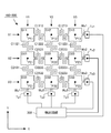
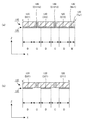
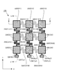
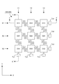
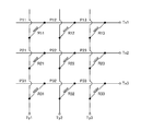
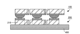
はじめに、本発明の基本的実施形態に係る触覚センサの全体構造を説明する。図1に示すとおり、この触覚センサは、網状本体部100+200と検出回路300とによって構成される。図1の上段は、網状本体部100+200の上面図、下段は検出回路300のブロック図である。ここでは、各部の配置を説明する便宜上、図示のとおり、XYZ三次元座標系を定義することにする。具体的には、図1上段の上面図では、図の右方向にX軸、図の上方向にY軸、図の紙面垂直方向にZ軸が定義されている。
<<< §1. Overall structure of a tactile sensor according to a basic embodiment >>
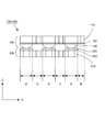
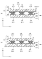
First, the entire structure of a tactile sensor according to a basic embodiment of the present invention will be described. As shown in FIG. 1, this tactile sensor is constituted by a net-like
一方、図2は、図1に示す触覚センサの網状本体部の側面図であり、図の右方向にX軸、図の上方向にZ軸、図の紙面垂直方向にY軸が定義されている。図示のとおり、網状本体部は、上部網状部材100と下部網状部材200とを上下に積層することにより構成される構造体であり、ここでは便宜上、符号「100+200」で示すことにする。この網状本体部100+200は、本発明に係る触覚センサの物理的な構造部分に相当する。検出回路300は、この網状本体部100+200の各部の電気的特性(電気抵抗)の変化に基づいて、各部に作用した外力を検出する機能を果たす。
On the other hand, FIG. 2 is a side view of the mesh body portion of the tactile sensor shown in FIG. Yes. As shown in the figure, the net-like main body is a structure formed by stacking an upper mesh-
図1の上面図に示されているとおり、この基本的実施形態の場合、XY平面上に3行3列の行列が定義されており、行列の第1行目X1,第2行目X2,第3行目X3はX軸に平行な方向を向き、行列の第1列目Y1,第2列目Y2,第3列目Y3はY軸に平行な方向を向いている。この3行3列の行列を構成する位置に、合計9個の検出点P11〜P33が配置されており、各検出点P11〜P33の位置には、作用した外力に基づいてその電気的特性に変化が生じる検出素子D11〜D33が配置されている。各検出点P11〜P33に作用した個々の外力は、検出素子D11〜D33によってそれぞれ独立して検出されることになる。 As shown in the top view of FIG. 1, in this basic embodiment, a 3 × 3 matrix is defined on the XY plane, and the first row X1, the second row X2, The third row X3 is oriented in the direction parallel to the X axis, and the first column Y1, the second column Y2, and the third column Y3 of the matrix are oriented in the direction parallel to the Y axis. A total of nine detection points P11 to P33 are arranged at positions constituting this 3 × 3 matrix, and the electrical characteristics of the detection points P11 to P33 are determined based on the applied external force. Detection elements D11 to D33 in which changes occur are arranged. Individual external forces acting on the detection points P11 to P33 are detected independently by the detection elements D11 to D33.
なお、本願明細書では、便宜上、3行3列の行列を構成する位置に配置された9個の検出点P11〜P33に作用した外力を、各検出点の位置に配置された9個の検出素子D11〜D33によって検出する例を実施例として述べるが、本発明における検出点(検出素子)の配置は、3行3列の行列に限定されるものではなく、5行5列、4行8列など、任意の行列配置であってかまわない。要するに、本発明に係る触覚センサは、m行n列の行列を構成する位置に配置されたm×n個の検出点に作用した個々の外力を、それぞれ独立して検出する機能をもったセンサであり、作用した外力に基づいてその電気的特性に変化が生じるm×n個の検出素子が各検出点の位置に配置されていればよい。 In the present specification, for the sake of convenience, the external forces acting on the nine detection points P11 to P33 arranged at the positions constituting the 3 × 3 matrix are detected as nine detections arranged at the positions of the respective detection points. An example in which detection is performed by the elements D11 to D33 will be described as an example. However, the arrangement of detection points (detection elements) in the present invention is not limited to a matrix of 3 rows and 3 columns, but 5 rows, 5 columns, 4 rows 8 Arbitrary matrix arrangements such as columns may be used. In short, the tactile sensor according to the present invention is a sensor having a function of independently detecting individual external forces acting on m × n detection points arranged at positions constituting a matrix of m rows and n columns. It is sufficient that m × n detection elements that change in their electrical characteristics based on the applied external force are arranged at the positions of the respective detection points.
図示の例は、m=n=3として、3行3列の行列を定義した一実施例ということになる。したがって、以下の具体的な説明では、図示のとおり3行3列の行列を定義した実施例についての説明を行うが、一般論としては、任意のm,n(但し、m≧2,n≧2)について定義されたm行n列の行列を定義して、本発明を実施することが可能である。そこで、本願明細書では、一般論としての説明を行う際には、変数i(i=1〜m)を行列の行番号を示すパラメータとして用い、変数j(j=1〜n)を行列の列番号を示すパラメータとして用いることにする。 The illustrated example is an embodiment in which a matrix of 3 rows and 3 columns is defined with m = n = 3. Therefore, in the following specific description, an embodiment in which a matrix of 3 rows and 3 columns is defined as shown in the figure will be described. However, as a general theory, any m, n (where m ≧ 2, n ≧ It is possible to implement the present invention by defining an m-by-n matrix defined for 2). Therefore, in the present specification, when explaining as a general theory, the variable i (i = 1 to m) is used as a parameter indicating the row number of the matrix, and the variable j (j = 1 to n) is used as the matrix. It is used as a parameter indicating the column number.
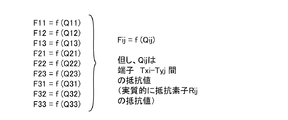
結局、本発明に係る触覚センサでは、m行n列の行列の第i行第j列目に配置された検出点Pijの位置に、第i行第j列目の検出素子Dijが配置されており、検出点Pijに作用した外力が、検出素子Dijによって検出されることになる。 After all, in the tactile sensor according to the present invention, the detection element Dij in the i-th row and the j-th column is arranged at the position of the detection point Pij arranged in the i-th row and the j-th column of the m-row and n-column matrix. Thus, the external force acting on the detection point Pij is detected by the detection element Dij.
図1の上面図に示されているとおり、9個の検出素子D11〜D33は、行方向接続部および列方向接続部(いずれも、4桁の数字に文字Cを冠した符号で示す)によって相互に接続されている。 As shown in the top view of FIG. 1, the nine detection elements D11 to D33 are constituted by a row-direction connection portion and a column-direction connection portion (both are indicated by a four-digit number with a letter C). Are connected to each other.
たとえば、検出素子D11とD12とは、行方向接続部C1112によって相互に接続されており、検出素子D12とD13とは、行方向接続部C1213によって相互に接続されている。ここで、行方向接続部C1112の符号に含まれる4桁の数字「1112」は、検出素子D11,D12に含まれる数字「11」,「12」を羅列したものであり、行方向接続部C1213の符号に含まれる4桁の数字「1213」は、検出素子D12,D13に含まれる数字「12」,「13」を羅列したものである。 For example, the detection elements D11 and D12 are connected to each other by a row direction connection portion C1112, and the detection elements D12 and D13 are connected to each other by a row direction connection portion C1213. Here, the four-digit number “1112” included in the reference numeral of the row direction connection portion C1112 is an enumeration of the numbers “11” and “12” included in the detection elements D11 and D12, and the row direction connection portion C1213. The four-digit number “1213” included in the reference numeral is a list of the numbers “12” and “13” included in the detection elements D12 and D13.
同様に、検出素子D11とD21とは、列方向接続部C1121によって相互に接続されており、検出素子D21とD31とは、列方向接続部C2131によって相互に接続されている。ここで、列方向接続部C1121の符号に含まれる4桁の数字「1121」は、検出素子D11,D21に含まれる数字「11」,「21」を羅列したものであり、列方向接続部C2131の符号に含まれる4桁の数字「2131」は、検出素子D21,D31に含まれる数字「21」,「31」を羅列したものである。 Similarly, the detection elements D11 and D21 are connected to each other by a column direction connection portion C1121, and the detection elements D21 and D31 are connected to each other by a column direction connection portion C2131. Here, the four-digit number “1121” included in the code of the column direction connection portion C1121 is a list of the numbers “11” and “21” included in the detection elements D11 and D21, and the column direction connection portion C2131. The four-digit number “2131” included in the reference numeral is an enumeration of the numbers “21” and “31” included in the detection elements D21 and D31.
結局、図1に示す実施形態の場合、9個の検出素子D11〜D33は、6組の行方向接続部C1112,C1213,C2122,C2223,C3132,C3233によって相互に行方向に接続され、6組の列方向接続部C1121,C2131,C1222,C2232,C1323,C2333によって相互に列方向に接続されている。6組の行方向接続部は、行方向に隣接する各検出素子対を相互に接続する役割を果たし、6組の列方向接続部は、列方向に隣接する各検出素子対を相互に接続する役割を果たす。より具体的には、各行方向接続部は、検出素子DijとDi(j+1)とを相互に接続する役割を果たし(但し、i=1〜m,j=1〜n−1)、各列方向接続部は、検出素子DijとD(i+1)jとを相互に接続する役割を果たす(但し、i=1〜m−1,j=1〜n)。 After all, in the case of the embodiment shown in FIG. 1, nine detection elements D11 to D33 are connected to each other in the row direction by six sets of row direction connection portions C1112, C1213, C2122, C2223, C3132, and C3233, and six sets Are connected to each other in the column direction by the column direction connection portions C1121, C2131, C1222, C2232, C1323, and C2333. The six sets of row direction connection portions serve to connect the detection element pairs adjacent in the row direction to each other, and the six sets of column direction connection portions connect the detection element pairs adjacent in the column direction to each other. Play a role. More specifically, each row direction connection portion serves to connect the detection elements Dij and Di (j + 1) to each other (where i = 1 to m, j = 1 to n−1), and each column direction. The connecting part plays a role of connecting the detection elements Dij and D (i + 1) j to each other (where i = 1 to m−1, j = 1 to n).
更に、図示の実施例の場合、配線の便宜を考慮して、行列の第4列目に相当する各位置に、行方向配線部Wx1〜Wx3を介して行方向端子部Tx1〜Tx3が設けられており、行列の第4行目に相当する各位置に、列方向配線部Wy1〜Wy3を介して列方向端子部Ty1〜Ty3が設けられている。これら各端子部Tx1〜Tx3,Ty1〜Ty3と検出回路300との間には配線が施され、検出回路300は、特定の検出素子Dijに生じた電気的特性の変化に基づいて、当該検出素子Dijが配置されている検出点Pijに作用した外力を検出する機能を果たす。
Further, in the illustrated embodiment, in consideration of the convenience of wiring, row direction terminal portions Tx1 to Tx3 are provided at respective positions corresponding to the fourth column of the matrix via the row direction wiring portions Wx1 to Wx3. In each position corresponding to the fourth row of the matrix, column direction terminal portions Ty1 to Ty3 are provided via column direction wiring portions Wy1 to Wy3. Each of the terminal portions Tx1 to Tx3, Ty1 to Ty3 and a
図1の上面図に示すとおり、各行方向接続部および各列方向接続部C1121〜C3233は、平面形状がクランク状の屈曲構造を有しており、行方向もしくは列方向に隣接する任意の検出素子対について、両者の三次元空間上での相互位置関係が、三次元の自由度をもって変化できるような可撓性を有している。このため、9個の検出素子D11〜D33の相互位置は、それぞれ三次元の自由度をもって自由に変化させることができる。 As shown in the top view of FIG. 1, each row direction connection portion and each column direction connection portion C1121 to C3233 have a bent structure with a crank shape in plan view, and are arbitrary detection elements adjacent in the row direction or the column direction. The pair has such flexibility that the mutual positional relationship in the three-dimensional space can be changed with a three-dimensional degree of freedom. Therefore, the mutual positions of the nine detection elements D11 to D33 can be freely changed with three-dimensional degrees of freedom.
別言すれば、図1および図2には、9個の検出素子D11〜D33が同一の平面上(XY平面に平行な平面上)に配置されている基本形態が示されているが、この網状本体部は、可撓性を有する行方向接続部および列方向接続部を屈曲させることにより任意曲面に沿った形状に変形させることが可能である。このように、本発明に係る触覚センサは、網状本体部を任意曲面に沿った形状に変形させた状態で対象物に取り付けることが可能であり、たとえば、人型ロボットの指先のように、球面に近い曲面に装着することができる。この場合、9個の検出素子D11〜D33および9個の検出点P11〜P33は、球面に近い曲面上に定義されたm行n列の行列状に配置された状態になる。 In other words, FIG. 1 and FIG. 2 show a basic form in which nine detection elements D11 to D33 are arranged on the same plane (on a plane parallel to the XY plane). The net-like main body can be deformed into a shape along an arbitrary curved surface by bending the flexible row-direction connecting portion and column-direction connecting portion. As described above, the tactile sensor according to the present invention can be attached to an object in a state where the net-like main body is deformed into a shape along an arbitrary curved surface. For example, a spherical surface like a fingertip of a humanoid robot can be attached. It can be attached to a curved surface close to. In this case, the nine detection elements D11 to D33 and the nine detection points P11 to P33 are arranged in a matrix of m rows and n columns defined on a curved surface close to a spherical surface.
図示の例のように、行方向接続部および列方向接続部を平面形状(XY平面への投影像)がクランク状の部材によって構成すると、両端に接続された一対の検出素子の相互位置関係を三次元の自由度をもって自由に変化させる構造を容易に実現することができる。たとえば、一対の検出素子D11,D12を接続する行方向接続部C1112として、図示のような平面形状がクランク状の部材を用いると、当該部材は、図のX軸方向に伸縮可能であるため、検出素子D11,D12のX軸方向に関する相互位置は所定の自由度をもって変化させることができる。 As in the example shown in the figure, when the row direction connection portion and the column direction connection portion are configured by a crank-shaped member having a planar shape (projected image on the XY plane), the mutual positional relationship between a pair of detection elements connected to both ends is obtained. A structure that can be freely changed with a three-dimensional degree of freedom can be easily realized. For example, as the row direction connecting portion C1112 that connects the pair of detection elements D11 and D12, if a member having a crank shape as shown in the drawing is used, the member can be expanded and contracted in the X-axis direction in the figure. The mutual positions of the detection elements D11 and D12 in the X-axis direction can be changed with a predetermined degree of freedom.
また、行方向接続部C1112のクランク状構造部を構成する一対のU字状部の姿勢の変化により、検出素子D11,D12のY軸方向に関する相互位置も所定の自由度をもって変化させることができる。更に、上記U字状部の上面側の開閉状態と下面側の開閉状態とを別個に調整すれば、検出素子D11,D12のZ軸方向に関する相互位置も所定の自由度をもって変化させることができる。 Further, the mutual positions of the detection elements D11 and D12 in the Y-axis direction can be changed with a predetermined degree of freedom by changing the postures of the pair of U-shaped portions constituting the crank-shaped structure portion of the row direction connection portion C1112. . Furthermore, if the open / close state on the upper surface side and the open / close state on the lower surface side of the U-shaped portion are separately adjusted, the mutual positions of the detection elements D11 and D12 in the Z-axis direction can be changed with a predetermined degree of freedom. .
なお、図示の実施例では、行方向接続部および列方向接続部を、平面形状がクランク状の部材、すなわち、直角に屈曲させた構造体によって構成しているが、屈曲部分は必ずしも直角構造面にする必要はなく、曲面構造によって構成してもかまわない。たとえば、平面形状(XY平面への投影像)がS字状となる屈曲構造を採用した場合にも、同様に、三次元の自由度をもって自由に変化させる構造を実現することができる。 In the illustrated embodiment, the row-direction connecting portion and the column-direction connecting portion are constituted by a crank-shaped member, that is, a structure bent at a right angle, but the bent portion is not necessarily a right-angle structure surface. It is not necessary to use a curved surface structure. For example, even when a bending structure in which the planar shape (projected image on the XY plane) is S-shaped is adopted, a structure that can be freely changed with three-dimensional degrees of freedom can be realized.
このように、クランク状もしくはS字状の屈曲構造を採用すると、両端点間の距離を容易に伸縮させることができるので、いわば絆創膏を指先に張り付けるように、網状本体部を人型ロボットの指先部分に装着することができるようになる。特に、図示する実施例のようなクランク状の屈曲構造は、直線的な加工によって実現することができるので、量産品としての触覚センサを製造する上では好ましい。 As described above, when the crank-shaped or S-shaped bending structure is adopted, the distance between the two end points can be easily expanded and contracted, so that the net-like main body portion of the humanoid robot can be attached to the fingertips. It can be attached to the fingertip portion. In particular, the crank-like bending structure as shown in the illustrated embodiment can be realized by linear processing, which is preferable in manufacturing a tactile sensor as a mass-produced product.
また、図示の実施例では、行方向配線部Wx1〜Wx3および列方向配線部Wy1〜Wy3もある程度の可撓性を有しており、行方向端子部Tx1,Tx2,Tx3とこれに隣接配置された検出素子D13,D23,D33との相互位置関係や、列方向端子部Ty1,Ty2,Ty3とこれに隣接配置された検出素子D31,D32,D33との相互位置関係も、ある程度の自由度をもって変化させることができる。もちろん、行方向配線部Wx1〜Wx3および列方向配線部Wy1〜Wy3についても、クランク状もしくはS字状の屈曲構造を採用してもかまわない。 In the illustrated embodiment, the row direction wiring portions Wx1 to Wx3 and the column direction wiring portions Wy1 to Wy3 also have a certain degree of flexibility, and are arranged adjacent to the row direction terminal portions Tx1, Tx2, Tx3. The mutual positional relationship between the detection elements D13, D23, and D33 and the mutual positional relationship between the column-direction terminal portions Ty1, Ty2, and Ty3 and the detection elements D31, D32, and D33 disposed adjacent thereto have a certain degree of freedom. Can be changed. Of course, a crank-shaped or S-shaped bent structure may be adopted for the row direction wiring portions Wx1 to Wx3 and the column direction wiring portions Wy1 to Wy3.
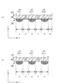
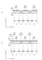
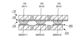
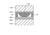
図1の上面図に示す網状本体部100+200は、実際には、図2の側面図に示すとおり、上部網状部材100と下部網状部材200とを上下に積層することにより構成される構造体である。図示のとおり、上部網状部材100は、上から順に、上部支持層110,上部電極層120,変形体層130の3層を積層した構造を有し、下部網状部材200は、下から順に、下部支持層210,下部電極層220,抵抗体層230の3層を積層した構造を有する。これら各層の平面形状は、§2において詳述する。
The net-like
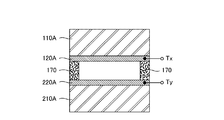
図2の下方に示されている矢印Dは検出領域Dの区間を示しており、矢印Cは接続領域Cの区間を示しており、矢印Wは配線領域Wの区間を示している。ここで、検出領域Dは、図1の上面図において、検出素子D11〜D33が配置された個々の正方形領域であり、接続領域Cは、検出素子D11〜D33を相互に接続するための各接続部C1112〜C3233が配置された個々の領域であり、配線領域Wは、各配線部Wx1〜Wx3,Wy1〜Wy3およ各端子部Tx1〜Tx3,Ty1〜Ty3が配置された個々の領域である。 An arrow D shown in the lower part of FIG. 2 indicates a section of the detection area D, an arrow C indicates a section of the connection area C, and an arrow W indicates a section of the wiring area W. Here, the detection region D is an individual square region in which the detection elements D11 to D33 are arranged in the top view of FIG. 1, and the connection region C is each connection for connecting the detection elements D11 to D33 to each other. The wiring areas W are individual areas where the wiring parts Wx1 to Wx3, Wy1 to Wy3 and the terminal parts Tx1 to Tx3, Ty1 to Ty3 are arranged. .
したがって、図1の上面図に正方形で示されている1つの検出素子は、実際には、図2の側面図において検出領域Dに配置された6層(上から下に順に、110,120,130,230,220,210の各層)からなる構造体によって構成されていることになる。また、図1の上面図にクランク状の部材として描かれている各接続部は、実際には、上部網状部材100側の接続領域Cに配置された上方部材と、下部網状部材200側の接続領域Cに配置された下方部材と、によって構成されていることになる。
Therefore, one detection element indicated by a square in the top view of FIG. 1 actually has six layers (110, 120,... In order from the top to the bottom) arranged in the detection region D in the side view of FIG. 130, 230, 220, and 210). Moreover, each connection part drawn as a crank-shaped member in the top view of FIG. 1 is actually a connection between the upper member disposed in the connection region C on the
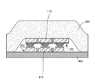
図2に示すとおり、上部網状部材100は、上部支持層110と、この上部支持層110の下面に形成された上部電極層120と、この上部電極層120の下面に形成された変形体層130と、を有し、下部網状部材200は、下部支持層210と、この下部支持層210の上面に形成された下部電極層220と、この下部電極層220の上面に形成された抵抗体層230と、を有している。
As shown in FIG. 2, the
ここで、上部電極層120のうち、各検出領域Dに位置する正方形状の部分は上部個別電極層を形成し、下部電極層220のうち、各検出領域Dに位置する正方形状の部分は下部個別電極層を形成する。そして、各検出素子D11〜D33における外力検出は、上方に配置された上部個別電極層と、この上部個別電極層に対向するように下方に配置された下部個別電極層と、これら一対の個別電極層間に介挿された中間要素(図2に示す実施形態の場合は、変形体層130と抵抗体層230のうち、各検出領域Dに位置する部分)とを利用して行われる。
Here, in the
すなわち、上記中間要素は、上下一対の個別電極層間の間隔を縮める方向に外力が作用すると、少なくともその一部が弾性変形を生じ、外力が作用しなくなったときに当該間隔を元に復元させる性質をもち、かつ、当該間隔の変化に応じて上下一対の個別電極層間の電気抵抗を変化させる性質をもっている。したがって、検出回路300は、この電気抵抗に基づいて、作用した外力を検出することができる。このような外力検出の具体的な原理については、§3で詳述する。
In other words, the intermediate element has a property that when an external force is applied in a direction to reduce the distance between the pair of upper and lower individual electrode layers, at least a part thereof is elastically deformed and restored based on the interval when the external force stops working. And has the property of changing the electrical resistance between the pair of upper and lower individual electrode layers in accordance with the change in the interval. Therefore, the
<<< §2. 基本的実施形態に係る触覚センサの各部の構造 >>>
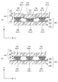
続いて、§1で述べた基本的実施形態に係る触覚センサを構成する網状本体部100+200の各部の構造を、図3〜図14を参照しながら詳細に説明する。この図3〜図14においても、図1,図2に示されたXYZ三次元座標系と同一の座標系を定義して各部の配置を示すことにする。なお、本願の各図は、触覚センサの構造を図面として明瞭に示すため、各部の実際の寸法比とは異なる寸法比で描かれている。そこで、以下の説明では、必要に応じて、各部の実寸を数値として例示することにする。
<<< §2. Structure of each part of tactile sensor according to basic embodiment >>
Next, the structure of each part of the
図2の側面図に示すとおり、網状本体部100+200は、上部網状部材100と下部網状部材200とによって構成されており、全体的には、図1の上面図に示すとおり、9個の検出素子D11〜D33を各接続部によって縦横に接続した網状構造を有している。
As shown in the side view of FIG. 2, the net-like
<2−1.上部網状部材100の構造>
ここでは、まず、上部網状部材100の構造について説明する。図2に示すとおり、上部網状部材100は、上部支持層110、上部電極層120、変形体層130の3層構造からなる。図3は、図2に示す触覚センサの上部支持層110のみを示す上面図である。この図3に示されている上部支持層110の平面形状は、図1に示されている網状本体部100+200全体の平面形状とほぼ同じであるが、列方向配線部Wy1〜Wy3および列方向端子部Ty1〜Ty3は、下部網状部材200の構成要素であるため、図3には描かれていない。
<2-1. Structure of
Here, first, the structure of the
図3に示すとおり、この上部支持層110は、3行3列の行列を構成するように配置された9個の正方形状の上部検出素片110(D11)〜110(D33)と、行方向に隣接する一対の上部検出素片を相互に接続する可撓性をもった上部行方向接続部110(C1112),110(C1213),110(C2122),110(C2223),110(C3132),110(C3233)と、列方向に隣接する一対の上部検出素片を相互に接続する可撓性をもった上部列方向接続部110(C1121),110(C2131),110(C1222),110(C2232),110(C1323),110(C2333)と、を有している。ここで、上部行方向接続部および上部列方向接続部は、図示のとおり、平面形状がクランク状(もしくはS字状でもよい)の屈曲構造を有する。
As shown in FIG. 3, the
なお、これらの各部材の符号の前半部「110」は、当該部材が上部支持層110の一部分を構成することを示しており、後半部の括弧内の符号は、図1に示す網状本体部100+200の各部分に対応することを示している。たとえば、上部検出素片110(D11)の符号「110(D11)」は、当該部材が、上部支持層110のうちの検出素子D11に所属する部分であることを示している。以下に述べる各部材についても同様である。
In addition, the first half “110” of the reference numerals of these members indicates that the members constitute a part of the
ここに示す実施例の場合、配線の便宜を考慮して、この上部支持層110の右端部分には、更に、行列の第4列目に相当する各位置に3個の上部行方向端子支持部110(Tx1),110(Tx2),110(Tx3)が設けられており、行列の第3列目に配置された3個の上部検出素片110(D13),110(D23),110(D33)と、上記上部行方向端子支持部110(Tx1),110(Tx2),110(Tx3)とをそれぞれ相互に接続するための上部行方向配線支持部110(Wx1),110(Wx2),110(Wx3)が設けられている。
In the case of the embodiment shown here, in consideration of the convenience of wiring, the
一般論で述べれば、上部支持層110は、m行n列の行列を構成するように配置されたm×n個の上部検出素片と、第i行目(i=1〜m)に配列されたn個の上部検出素片のうち、それぞれ隣接する一対の上部検出素片を相互に接続する可撓性をもった上部行方向接続部と、第j列目(j=1〜n)に配列されたm個の上部検出素片のうち、それぞれ隣接する一対の上部検出素片を相互に接続する可撓性をもった上部列方向接続部と、を有している。ここで、上部行方向接続部および上部列方向接続部は、それぞれ両端に接続された一対の上部検出素片の三次元空間上での相互位置関係が、三次元の自由度をもって変化できるように、当該一対の上部検出素片を接続する機能を有する。
Generally speaking, the
また、上部支持層110は、配線の便宜を考慮して、行列の第i行第(n+1)列目(i=1〜m)に相当する各位置に配置されたm個の上部行方向端子支持部と、行列の第i行第n列目(i=1〜m)に配置されたm個の上部検出素片と前記m個の上部行方向端子支持部とをそれぞれ相互に接続するm個の上部行方向配線支持部と、を更に有している。
Further, the
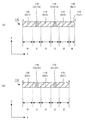
図4(a) は、図3に示す上部支持層110を切断線a−a′の位置で切断した側断面図(行方向断面図)であり、左から右に向かって、上部検出素片110(D11),上部行方向接続部110(C1112),上部検出素片110(D12),上部行方向接続部110(C1213),上部検出素片110(D13),上部行方向配線支持部110(Wx1),上部行方向端子支持部110(Tx1)が連続配置されている状態が示されている。
FIG. 4A is a side cross-sectional view (a cross-sectional view in the row direction) obtained by cutting the
一方、図4(b) は、図3に示す上部支持層110を切断線b−b′の位置で切断した側断面図(列方向断面図)であり、右から左に向かって、上部検出素片110(D11),上部列方向接続部110(C1121),上部検出素片110(D21),上部列方向接続部110(C2131),上部検出素片110(D31)が連続配置されている状態が示されている。
On the other hand, FIG. 4B is a side sectional view (column direction sectional view) obtained by cutting the
図4に示すとおり、上部支持層110は、一定の厚みをもった平板によって構成され、上部網状部材100の支持媒体として機能する。§1で述べたとおり、行方向接続部および列方向接続部は、クランク状(S字状でもよい)の屈曲構造を有しているため可撓性をもち、隣接する各上部検出素片の三次元空間上での相互位置関係は、三次元の自由度をもって変化させることができる。したがって、この上部支持層110は、人型ロボットの指先のように、球面に近い曲面に装着することが可能である。
As shown in FIG. 4, the
上部支持層110の材質は、各上部検出素片の部分が上部電極層および変形体層の支持媒体として機能することができ、行方向接続部および列方向接続部の部分が上記可撓性を有するという条件を満たす材質であれば、どのような材質を用いてもかまわない。実用上は、加工の便宜を考慮して、ポリイミドやPETなどの樹脂によって上部支持層110を構成すればよい。あるいは、ガラスエポキシ基板やセラミック基板によって上部支持層110を構成してもかまわない。
As for the material of the
ここに示す実施例の場合、厚み0.1mmのポリイミドのシートを、図3に示すような形状に加工して上部支持層110として用いている。また、上部検出素片110(D11)〜110(D33)は、一辺が2mmの正方形となるようにし、隣接する一対の上部検出素片の間隔(上部行方向接続部および上部列方向接続部の両端点距離)を、1.6mmに設定している。一方、上部行方向接続部および上部列方向接続部の幅は、0.4mmに設定し、十分な可撓性が得られるようにしている。
In the example shown here, a polyimide sheet having a thickness of 0.1 mm is processed into a shape as shown in FIG. 3 and used as the
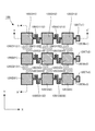
図5は、図2に示す触覚センサの上部電極層120の平面形状を示すパターン図であり、上方から見たパターンを示す。位置関係を明確にするため、上部支持層110の平面形状を併せて描いてある。実際には、上部電極層120は、上部支持層110の下面に形成される層である。図に太線枠で囲ってハッチングを施した部分が、上部電極層120を構成するパターンである(ハッチングは、上部電極層120の平面形状を示すためのものであり、断面を示すものではない)。結局、上部電極層120は、上部支持層110の下面における上部列方向接続部を除く全領域(ハッチングした領域)に形成されていることになる。
FIG. 5 is a pattern diagram showing a planar shape of the
ここでは、上部検出素片110(D11)〜110(D33)の下面に形成された電極層を、それぞれ上部個別電極層120(D11)〜120(D33)と呼び、上部行方向接続部110(C1112),110(C1213),110(C2122),110(C2223),110(C3132),110(C3233)の下面に形成された電極層を、それぞれ上部行方向接続電極層120(C1112),120(C1213),120(C2122),120(C2223),120(C3132),120(C3233)と呼ぶことにする。また、上部行方向配線支持部110(Wx1)〜110(Wx3)の下面に形成された電極層を、それぞれ上部行方向配線層120(Wx1)〜120(Wx3)と呼び、上部行方向端子支持部110(Tx1)〜110(Tx3)の下面に形成された電極層を、それぞれ上部行方向端子層120(Tx1)〜120(Tx3)と呼ぶことにする。 Here, the electrode layers formed on the lower surfaces of the upper detection pieces 110 (D11) to 110 (D33) are referred to as upper individual electrode layers 120 (D11) to 120 (D33), respectively, and the upper row direction connection portion 110 ( C1112), 110 (C1213), 110 (C2122), 110 (C2223), 110 (C3132), and 110 (C3233) are formed on the lower surface by connecting the electrode layers to the upper row connection electrode layers 120 (C1112) and 120, respectively. These are referred to as (C1213), 120 (C2122), 120 (C2223), 120 (C3132), and 120 (C3233). Also, the electrode layers formed on the lower surfaces of the upper row direction wiring support portions 110 (Wx1) to 110 (Wx3) are referred to as upper row direction wiring layers 120 (Wx1) to 120 (Wx3), respectively. The electrode layers formed on the lower surfaces of the portions 110 (Tx1) to 110 (Tx3) will be referred to as upper row direction terminal layers 120 (Tx1) to 120 (Tx3), respectively.
図示のとおり、上部電極層120は、電気的に独立した3つの群に分けられる。すなわち、行列の第1行目には、上部個別電極層120(D11),上部行方向接続電極層120(C1112),上部個別電極層120(D12),上部行方向接続電極層120(C1213),上部個別電極層120(D13),上部行方向配線層120(Wx1),上部行方向端子層120(Tx1)からなる相互に電気的に接続された第1電極群が形成されている。これら第1電極群は、第1番目の行方向導電路を形成し、上部行方向端子層120(Tx1)は、この第1番目の行方向導電路に対する外部配線用の端子として機能する。
As shown, the
同様に、行列の第2行目には、上部個別電極層120(D21),上部行方向接続電極層120(C2122),上部個別電極層120(D22),上部行方向接続電極層120(C2223),上部個別電極層120(D23),上部行方向配線層120(Wx2),上部行方向端子層120(Tx2)からなる相互に電気的に接続された第2電極群が形成されている。これら第2電極群は、第2番目の行方向導電路を形成し、上部行方向端子層120(Tx2)は、この第2番目の行方向導電路に対する外部配線用の端子として機能する。 Similarly, in the second row of the matrix, the upper individual electrode layer 120 (D21), the upper row direction connection electrode layer 120 (C2122), the upper individual electrode layer 120 (D22), and the upper row direction connection electrode layer 120 (C2223). ), An upper individual electrode layer 120 (D23), an upper row direction wiring layer 120 (Wx2), and an upper row direction terminal layer 120 (Tx2), which are electrically connected to each other, are formed. These second electrode groups form a second row direction conductive path, and the upper row direction terminal layer 120 (Tx2) functions as a terminal for external wiring with respect to the second row direction conductive path.
そして、行列の第3行目には、上部個別電極層120(D31),上部行方向接続電極層120(C3132),上部個別電極層120(D32),上部行方向接続電極層120(C3233),上部個別電極層120(D33),上部行方向配線層120(Wx3),上部行方向端子層120(Tx3)からなる相互に電気的に接続された第3電極群が形成されている。これら第3電極群は、第3番目の行方向導電路を形成し、上部行方向端子層120(Tx3)は、この第3番目の行方向導電路に対する外部配線用の端子として機能する。 In the third row of the matrix, the upper individual electrode layer 120 (D31), the upper row direction connection electrode layer 120 (C3132), the upper individual electrode layer 120 (D32), and the upper row direction connection electrode layer 120 (C3233). , An upper individual electrode layer 120 (D33), an upper row direction wiring layer 120 (Wx3), and an upper row direction terminal layer 120 (Tx3), which are electrically connected to each other, are formed. These third electrode groups form a third row direction conductive path, and the upper row direction terminal layer 120 (Tx3) functions as a terminal for external wiring with respect to the third row direction conductive path.
一般論で述べれば、上部電極層120は、各上部検出素片の下面に形成されたm×n個の上部個別電極層120(Dij)と、各上部行方向接続部の下面に形成された上部行方向接続電極層と、を有し、第i行目に配列された上部個別電極層および第i行目に配列された上部行方向接続電極層は相互に電気的に接続され、第i番目の行方向導電路を形成する。また、上部電極層120は、m個の上部行方向端子支持部の下面に形成されたm個の上部行方向端子層120(Txi)と、m個の上部行方向配線支持部の下面に形成されたm個の上部行方向配線層120(Wxi)と、を更に有し、第i番目の行方向導電路は、第i番目の上部行方向配線層120(Wxi)を介して第i番目の上部行方向端子層120(Txi)に電気的に接続されている。この上部行方向端子層120(Txi)は、この第i番目の行方向導電路に対する外部配線用の端子として機能することになる。
Generally speaking, the
図6(a) は、図3に示す上部支持層110の下面に図5に示す上部電極層120を形成した状態を、図5の切断線a−a′の位置で切断した側断面図(行方向断面図)であり、図6(b) は、同じ状態を、図5の切断線b−b′の位置で切断した側断面図(列方向断面図)である。図6(a) に示すように、行方向に関しては、上部電極層120が連続して形成され、行方向導電路が形成されているが、図6(b) に示すように、列方向に関しては、上部電極層120は離散的に形成されているため、各行方向導電路は、互いに電気的に独立している。
6A is a side cross-sectional view of the state in which the
上部電極層120の材質は、導電性を有し、かつ、クランク状の行方向接続部の撓みに応じて撓みを生じることが可能な材料であれば、どのような材料を用いてもかまわないが、実用上は、金属層によって上部電極層120を構成するのが好ましい。ここに示す実施例の場合、上部支持層110の下面の所定領域(図5にハッチングを施して示す領域)に、印刷の手法を用いて厚み0.05mm程度の銅箔を形成し、この銅箔を上部電極層120として用いている。この程度の厚みの銅箔であれば、クランク状の行方向接続部が撓みを生じても、これに応じた撓みを生じることができ、行方向導電路に断線が生じることはない。
The material of the
図7は、図2に示す触覚センサの変形体層130の平面形状を示すパターン図であり、上方から見たパターンを示す。ここでも位置関係を明確にするため、上部支持層110の平面形状を併せて描いてある。実際には、変形体層130は、上部支持層110の下面に形成された上部電極層120の更に下面に形成される層である。図に太線枠で囲ってハッチングを施した部分が、変形体層130を構成するパターンである(ハッチングは、変形体層130の平面形状を示すためのものであり、断面を示すものではない)。
FIG. 7 is a pattern diagram showing a planar shape of the
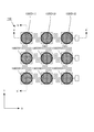
ここに示す実施例では、変形体層130は、正方形状をした各上部個別電極層120(D11)〜120(D33)の下面に接合された半球状(幾何学的に正確な半球ではなく、若干扁平している形状)の個別弾性変形体130(D11)〜130(D33)によって構成されているため、図7のパターン図では、各個別弾性変形体130(D11)〜130(D33)は円形のパターンを構成している。
In the embodiment shown here, the
図8(a) は、図2に示す触覚センサの上部網状部材100(すなわち、上部支持層110、上部電極層120、変形体層130の積層構造体)を、図7の切断線a−a′の位置で切断した側断面図(行方向断面図)であり、図8(b) は、切断線b−b′の位置で切断した側断面図(列方向断面図)である。ここで述べる基本的実施形態の場合、個別弾性変形体130(D11)〜130(D33)は、図示のとおり、各検出領域Dに配置された半球状の部材であり、弾性変形を生じる導電性材料によって構成されている。
FIG. 8A shows the
個別弾性変形体130(D11)〜130(D33)の材質は、弾性変形を生じる導電性材料(後述する変形例の場合は、弾性変形を生じる抵抗体材料)であれば、どのような材料を用いてもかまわないが、実用上は、導電性ゴムを用いるのが最適である。導電性ゴムは、主材となるゴム原料に所定量のカーボンや金属を添加したものであり、主材と添加物との割合を調整することにより抵抗率を調整することができる。 The material of the individual elastic deformation bodies 130 (D11) to 130 (D33) may be any material as long as it is a conductive material that generates elastic deformation (in the case of a modification described later, a resistor material that generates elastic deformation). Although it may be used, it is optimal to use conductive rubber for practical use. The conductive rubber is obtained by adding a predetermined amount of carbon or metal to a rubber material as a main material, and the resistivity can be adjusted by adjusting the ratio between the main material and the additive.
ここに示す実施例の場合、ほぼ導体としての性質を呈するように添加物の割合を調整した導電性ゴムを、半球状に成形したものを個別弾性変形体130(D11)〜130(D33)として用いている。なお、各個別弾性変形体の実寸は、直径2mm、高さ0.5mmであり、正確には幾何学的な半球よりも扁平したものになっている。 In the case of the example shown here, the conductive rubber whose ratio of the additive is adjusted so as to substantially exhibit the properties as a conductor, and those formed into a hemispherical shape are used as the individual elastic deformation bodies 130 (D11) to 130 (D33). Used. In addition, the actual size of each individual elastic deformation body is 2 mm in diameter and 0.5 mm in height, and more precisely, is flatter than a geometrical hemisphere.
個別弾性変形体130(D11)〜130(D33)の形状を半球状とするのは、§3で述べるように、下方に接することになる抵抗体層230との接触面積が、作用する外力に応じて変化するようにするためである。逆に言えば、作用する外力に応じて抵抗体層230との接触面積が変化する形状であれば、個別弾性変形体130(D11)〜130(D33)の形状は必ずしも半球状である必要はない。
The shape of each of the individual elastic deformation bodies 130 (D11) to 130 (D33) is hemispherical because, as described in §3, the contact area with the
要するに、個別弾性変形体130(D11)〜130(D33)は、上部個別電極層120(D11)〜120(D33)の下面から下方に凸となるように隆起した形状を有していればよいので、回転楕円体を切断した形状、放物線をその中心軸まわりに回転させた回転体形状、あるいは円錐形状などであってもかまわない。ただ、実用上は、作用した外力と接触面積との関係ができるだけ線形に近くなるように、球もしくは回転楕円体をその中心軸に直交する切断面で切断した立体形状を有する個別弾性変形体を用意し、当該切断面を上部個別電極層の下面に接続して用いるようにするのが好ましい。 In short, the individual elastic deformation bodies 130 (D11) to 130 (D33) may have a shape that protrudes downward from the lower surface of the upper individual electrode layers 120 (D11) to 120 (D33). Therefore, a shape obtained by cutting a spheroid, a shape of a rotator obtained by rotating a parabola around its central axis, a conical shape, or the like may be used. However, in practice, an individual elastic deformation body having a three-dimensional shape obtained by cutting a sphere or a spheroid with a cutting plane orthogonal to the central axis so that the relationship between the applied external force and the contact area is as close to linear as possible. It is preferable to prepare and use the cut surface by connecting it to the lower surface of the upper individual electrode layer.
一般論で述べれば、変形体層130は、m行n列の行列状に配置された各上部個別電極層の下面から、下方に凸となるように隆起した形状をなすm×n個の個別弾性変形体によって構成されており、各個別弾性変形体は導電体(この実施例の場合は導電性ゴム)からなり、その上面はそれぞれ上方に位置する個々の上部個別電極層の下面に接続されていることになる。
Generally speaking, the
<2−2.下部網状部材200の構造>
続いて、下部網状部材200の構造について説明する。図2に示すとおり、下部網状部材200は、下部支持層210、下部電極層220、抵抗体層230の3層構造からなる。図9は、図2に示す触覚センサの下部支持層210のみを示す上面図である。この図9に示されている下部支持層210の主たる構造は、図3に示す上部支持層110の構造とほぼ同じであり、両者の相違は、配線支持部および端子支持部の位置のみである。
<2-2. Structure of
Next, the structure of the
すなわち、図3に示す上部支持層110の場合、上部行方向配線支持部110(Wx1)〜110(Wx3)および上部行方向端子支持部110(Tx1)〜110(Tx3)が図の右方に配置されていたのに対して、図9に示す下部支持層210の場合、下部列方向配線支持部210(Wy1)〜210(Wy3)および下部列方向端子支持部110(Ty1)〜110(Ty3)は、図の下方に配置されている。このため、上部網状部材100の下方に下部網状部材200を積層配置すると、図1の上面図に示すように、両者の形状は平面的にほとんどの部分が重なり合い、下部網状部材200の列方向配線部Wy1〜Wy3および列方向端子部Ty1〜Ty3のみが、上部網状部材100の下方から食み出した状態になる。
That is, in the case of the
図9に示すとおり、下部支持層210は、3行3列の行列を構成するように配置された9個の正方形状の下部検出素片210(D11)〜210(D33)と、行方向に隣接する一対の下部検出素片を相互に接続する可撓性をもった下部行方向接続部210(C1112),210(C1213),210(C2122),210(C2223),210(C3132),210(C3233)と、列方向に隣接する一対の下部検出素片を相互に接続する可撓性をもった下部列方向接続部210(C1121),210(C2131),210(C1222),210(C2232),210(C1323),210(C2333)と、を有している。ここで、下部行方向接続部および下部列方向接続部は、図示のとおり、平面形状がクランク状(もしくはS字状でもよい)の屈曲構造を有する。
As shown in FIG. 9, the
更に、ここに示す実施例の場合、配線の便宜を考慮して、この下部支持層210の下端部分には、更に、行列の第4行目に相当する各位置に3個の下部列方向端子支持部210(Ty1),210(Ty2),210(Ty3)が設けられており、行列の第3行目に配置された3個の下部検出素片210(D31),210(D32),210(D33)と、上記下部列方向端子支持部210(Ty1),210(Ty2),210(Ty3)とをそれぞれ相互に接続するための下部列方向配線支持部210(Wy1),210(Wy2),210(Wy3)が設けられている。
Further, in the case of the embodiment shown here, in consideration of the convenience of wiring, the
一般論で述べれば、下部支持層210は、m行n列の行列を構成するように配置されたm×n個の下部検出素片と、第i行目(i=1〜m)に配列されたn個の下部検出素片のうち、それぞれ隣接する一対の下部検出素片を相互に接続する可撓性をもった下部行方向接続部と、第j列目(j=1〜n)に配列されたm個の下部検出素片のうち、それぞれ隣接する一対の下部検出素片を相互に接続する可撓性をもった下部列方向接続部と、を有している。ここで、下部行方向接続部および下部列方向接続部は、それぞれ両端に接続された一対の下部検出素片の三次元空間上での相互位置関係が、三次元の自由度をもって変化できるように、当該一対の下部検出素片を接続する機能を有する。
Generally speaking, the
また、下部支持層210は、配線の便宜を考慮して、行列の第(m+1)行第j列目(j=1〜n)に相当する各位置に配置されたn個の下部列方向端子支持部と、行列の第m行第j列目(j=1〜n)に配置されたn個の下部検出素片と前記n個の下部列方向端子支持部とをそれぞれ相互に接続するn個の下部列方向配線支持部と、を更に有している。
The
図10(a) は、図9に示す下部支持層210を切断線a−a′の位置で切断した側断面図(行方向断面図)であり、左から右に向かって、下部検出素片210(D11),下部行方向接続部210(C1112),下部検出素片210(D12),下部行方向接続部210(C1213),下部検出素片210(D13)が連続配置されている状態が示されている。
FIG. 10A is a side sectional view (a sectional view in the row direction) of the
一方、図10(b) は、図9に示す下部支持層210を切断線b−b′の位置で切断した側断面図(列方向断面図)であり、右から左に向かって、下部検出素片210(D11),下部列方向接続部210(C1121),下部検出素片210(D21),下部列方向接続部210(C2131),下部検出素片210(D31),下部列方向配線支持部210(Wy1),下部列方向端子支持部210(Ty1)が連続配置されている状態が示されている。
On the other hand, FIG. 10B is a side sectional view (column direction sectional view) obtained by cutting the
図10に示すとおり、下部支持層210は、一定の厚みをもった平板によって構成され、下部網状部材200の支持媒体として機能する。§1で述べたとおり、行方向接続部および列方向接続部は、クランク状(S字状でもよい)の屈曲構造を有しているため可撓性をもち、隣接する各下部検出素片の三次元空間上での相互位置関係は、三次元の自由度をもって変化させることができる。したがって、この下部支持層210は、上部支持層110と同様に、人型ロボットの指先のように、球面に近い曲面に装着することが可能である。
As shown in FIG. 10, the
下部支持層210の材質は、各下部検出素片の部分が下部電極層および抵抗体層の支持媒体として機能することができ、行方向接続部および列方向接続部の部分が上記可撓性を有するという条件を満たす材質であれば、どのような材質を用いてもかまわない。実用上は、上部支持層110と同様に、ポリイミドやPETなどの樹脂によって下部支持層210を構成すればよい。あるいは、ガラスエポキシ基板やセラミック基板によって下部支持層210を構成してもかまわない。
As for the material of the
ここに示す実施例の場合、厚み0.1mmのポリイミドのシートを、図9に示すような形状に加工して下部支持層210として用いている。また、下部検出素片210(D11)〜210(D33)は、上部検出素片110(D11)〜110(D33)と同様に、一辺が2mmの正方形となるようにし、隣接する一対の下部検出素片の間隔(下部行方向接続部および下部列方向接続部の両端点距離)を、1.6mmに設定している。一方、下部行方向接続部および下部列方向接続部の幅は、0.4mmに設定し、十分な可撓性が得られるようにしている。
In the embodiment shown here, a polyimide sheet having a thickness of 0.1 mm is processed into a shape as shown in FIG. 9 and used as the
図11は、図2に示す触覚センサの下部電極層220の平面形状を示すパターン図であり、上方から見たパターンを示す。位置関係を明確にするため、下部支持層210の平面形状を併せて描いてある。下部電極層220は、下部支持層210の上面に形成される層であるため、図11は、下部支持層210の上面に下部電極層220を形成した状態を示す上面図に相当する。図に太線枠で囲ってハッチングを施した部分が、下部電極層220を構成するパターンである(ハッチングは、下部電極層220の平面形状を示すためのものであり、断面を示すものではない)。結局、下部電極層220は、下部支持層210の上面における下部行方向接続部を除く全領域(ハッチングした領域)に形成されていることになる。
FIG. 11 is a pattern diagram showing a planar shape of the
ここでは、下部検出素片210(D11)〜210(D33)の上面に形成された電極層を、それぞれ下部個別電極層220(D11)〜220(D33)と呼び、下部列方向接続部210(C1121),210(C2131),210(C1222),210(C2232),210(C1323),210(C2333)の上面に形成された電極層を、それぞれ下部列方向接続電極層220(C1121),220(C2131),220(C1222),220(C2232),220(C1323),220(C2333)と呼ぶことにする。また、下部列方向配線支持部210(Wy1)〜210(Wy3)の上面に形成された電極層を、それぞれ下部列方向配線層220(Wy1)〜220(Wy3)と呼び、下部列方向端子支持部210(Ty1)〜210(Ty3)の上面に形成された電極層を、それぞれ下部列方向端子層220(Ty1)〜220(Ty3)と呼ぶことにする。 Here, the electrode layers formed on the upper surfaces of the lower detection pieces 210 (D11) to 210 (D33) are referred to as lower individual electrode layers 220 (D11) to 220 (D33), respectively, and the lower column direction connection portion 210 ( C1121), 210 (C2131), 210 (C1222), 210 (C2232), 210 (C1323), and 210 (C2333) are formed on the upper surface thereof by lower column direction connection electrode layers 220 (C1121) and 220, respectively. These are referred to as (C2131), 220 (C1222), 220 (C2232), 220 (C1323), and 220 (C2333). In addition, the electrode layers formed on the upper surfaces of the lower column direction wiring support portions 210 (Wy1) to 210 (Wy3) are referred to as lower column direction wiring layers 220 (Wy1) to 220 (Wy3), respectively. The electrode layers formed on the upper surfaces of the portions 210 (Ty1) to 210 (Ty3) will be referred to as lower column direction terminal layers 220 (Ty1) to 220 (Ty3), respectively.
図示のとおり、下部電極層220は、電気的に独立した3つの群に分けられる。すなわち、行列の第1列目には、下部個別電極層220(D11),下部列方向接続電極層220(C1121),下部個別電極層220(D21),下部列方向接続電極層220(C2131),下部個別電極層220(D31),下部列方向配線層220(Wy1),下部列方向端子層220(Ty1)からなる相互に電気的に接続された第1電極群が形成されている。これら第1電極群は、第1番目の列方向導電路を形成し、下部列方向端子層220(Ty1)は、この第1番目の列方向導電路に対する外部配線用の端子として機能する。
As shown, the
同様に、行列の第2列目には、下部個別電極層220(D12),下部列方向接続電極層220(C1222),下部個別電極層220(D22),下部列方向接続電極層220(C2232),下部個別電極層220(D32),下部列方向配線層220(Wy2),下部列方向端子層220(Ty2)からなる相互に電気的に接続された第2電極群が形成されている。これら第2電極群は、第2番目の列方向導電路を形成し、下部列方向端子層220(Ty2)は、この第2番目の列方向導電路に対する外部配線用の端子として機能する。 Similarly, in the second column of the matrix, the lower individual electrode layer 220 (D12), the lower column direction connection electrode layer 220 (C1222), the lower individual electrode layer 220 (D22), and the lower column direction connection electrode layer 220 (C2232). ), A lower individual electrode layer 220 (D32), a lower column direction wiring layer 220 (Wy2), and a lower column direction terminal layer 220 (Ty2), which are electrically connected to each other. These second electrode groups form a second column direction conductive path, and the lower column direction terminal layer 220 (Ty2) functions as an external wiring terminal for the second column direction conductive path.
そして、行列の第3列目には、下部個別電極層220(D13),下部列方向接続電極層220(C1323),下部個別電極層220(D23),下部列方向接続電極層220(C2333),下部個別電極層220(D33),下部列方向配線層220(Wy3),下部列方向端子層220(Ty3)からなる相互に電気的に接続された第3電極群が形成されている。これら第3電極群は、第3番目の列方向導電路を形成し、下部列方向端子層220(Ty3)は、この第3番目の列方向導電路に対する外部配線用の端子として機能する。 In the third column of the matrix, the lower individual electrode layer 220 (D13), the lower column direction connection electrode layer 220 (C1323), the lower individual electrode layer 220 (D23), and the lower column direction connection electrode layer 220 (C2333). , A lower individual electrode layer 220 (D33), a lower column direction wiring layer 220 (Wy3), and a lower column direction terminal layer 220 (Ty3), which are electrically connected to each other. The third electrode group forms a third column direction conductive path, and the lower column direction terminal layer 220 (Ty3) functions as a terminal for external wiring with respect to the third column direction conductive path.
一般論で述べれば、下部電極層220は、各下部検出素片の上面に形成されたm×n個の下部個別電極層220(Dij)と、各下部列方向接続部の上面に形成された下部列方向接続電極層220(Wyj)と、を有し、第j列目に配列された下部個別電極層および第j列目に配列された下部列方向接続電極層は相互に電気的に接続され、第j番目の列方向導電路を形成する。また、下部電極層220は、n個の下部列方向端子支持部の上面に形成されたn個の下部列方向端子層220(Tyj)と、n個の下部列方向配線支持部の上面に形成されたn個の下部列方向配線層220(Wyj)と、を更に有し、第j番目の列方向導電路は、第j番目の下部列方向配線層220(Wyj)を介して第j番目の下部列方向端子層220(Tyj)に電気的に接続されている。この下部列方向端子層220(Tyj)は、この第j番目の列方向導電路に対する外部配線用の端子として機能することになる。
Generally speaking, the
図12(a) は、図9に示す下部支持層210の上面に図11に示す下部電極層220を形成した状態を、図11の切断線a−a′の位置で切断した側断面図(行方向断面図)であり、図12(b) は、同じ状態を、図11の切断線b−b′の位置で切断した側断面図(列方向断面図)である。図12(b) に示すように、列方向に関しては、下部電極層220が連続して形成され、列方向導電路が形成されているが、図12(a) に示すように、行方向に関しては、下部電極層220は離散的に形成されているため、各列方向導電路は、互いに電気的に独立している。
FIG. 12A is a side sectional view of the state where the
下部電極層220の材質は、導電性を有し、かつ、クランク状の列方向接続部の撓みに応じて撓みを生じることが可能な材料であれば、どのような材料を用いてもかまわない。実用上は、上部電極層120と同様に、金属層によって下部電極層220を構成するのが好ましい。ここに示す実施例の場合、下部支持層210の上面の所定領域(図11にハッチングを施して示す領域)に、印刷の手法を用いて厚み0.05mm程度の銅箔を形成し、この銅箔を下部電極層220として用いている。この程度の厚みの銅箔であれば、クランク状の列方向接続部が撓みを生じても、これに応じた撓みを生じることができ、列方向導電路に断線が生じることはない。
The material of the
図13は、図2に示す触覚センサの抵抗体層230の平面形状を示すパターン図であり、上方から見たパターンを示す。ここでも位置関係を明確にするため、下部支持層210の平面形状を併せて描いてある。抵抗体層230は、下部支持層210の上面に形成された下部電極層220の更に上面に形成される層であるため、図13は、3層からなる下部網状部材200の上面図に相当する。図に太線枠で囲ってハッチングを施した部分が、抵抗体層230を構成するパターンである(ハッチングは、抵抗体層230の平面形状を示すためのものであり、断面を示すものではない)。
FIG. 13 is a pattern diagram showing a planar shape of the
ここに示す実施例では、抵抗体層230は、正方形状をした各下部個別電極層220(D11)〜220(D33)の上面に形成された同じ正方形状の個別抵抗体層230(D11)〜230(D33)によって構成されている。なお、抵抗体層230は、図11に示す下部列方向接続電極層220(C1121),220(C2131),220(C1222),220(C2232),220(C1323),220(C2333)の上面にも形成されるようにしてもかまわない。この場合、抵抗体層230を構成する平面パターンは、図11に示す下部電極層220の平面パターンと同じになる。
In the embodiment shown here, the
図14(a) は、図2に示す触覚センサの下部網状部材200(すなわち、下部支持層210、下部電極層220、抵抗体層230の積層構造体)を、図13の切断線a−a′の位置で切断した側断面図(行方向断面図)であり、図14(b) は、切断線b−b′の位置で切断した側断面図(列方向断面図)である。ここで述べる基本的実施形態の場合、個別抵抗体層230(D11)〜230(D33)は、平面形状が、下部個別電極層220(D11)〜220(D33)と同じ正方形をした電気抵抗を有する層によって構成されており、後述するように、その上面には、それぞれ個別弾性変形体130(D11)〜130(D33)の下端が接触することになる。
14A shows the
個別抵抗体層230(D11)〜230(D33)の材質は、後述する検出動作に適した電気抵抗を有する材料であれば、どのような材料を用いてもかまわない。ここに示す実施例の場合、ρ=20Ω・m程度の電気抵抗率を有する厚膜抵抗体を材料として用い、これを厚み0.05mm程度の層に形成したものを個別抵抗体層230(D11)〜230(D33)として用いている。 The material of the individual resistor layers 230 (D11) to 230 (D33) may be any material as long as the material has an electrical resistance suitable for the detection operation described later. In the embodiment shown here, a thick film resistor having an electrical resistivity of about ρ = 20 Ω · m is used as a material, and this is formed into a layer having a thickness of about 0.05 mm. ) To 230 (D33).
要するに、抵抗体層230は、m行n列の行列状に配置された各下部個別電極層の上面(すなわち、個々の検出領域D)に形成されたm×n個の個別抵抗体層によって構成すればよい。
In short, the
<2−3.網状本体部100+200の構造>
図2の側面図に示す網状本体部100+200は、§2−1で述べた上部網状部材100と§2−2で述べた下部網状部材200とを、図のように上下に積層することにより構成され、本発明に係る触覚センサの物理的な構造部分となる構成要素である。図15は、この網状本体部100+200の上面図である。本発明に係る触覚センサは、この網状本体部100+200に、更に検出回路300を付加することにより構成され、m行n列の行列を構成する位置に配置されたm×n個の検出点に作用した個々の外力を、それぞれ独立して検出する機能を有する。
<2-3. Structure of
2 is constructed by stacking the
図15に示す実施例の場合、3行3列の行列を構成する位置に合計9個の検出素子D11〜D33が配置されており、9箇所の検出点に作用した外力が、行方向端子部Tx1〜Tx3および列方向端子部Ty1〜Ty3に形成されている各端子層を介して電気的に検出されることになる。 In the case of the embodiment shown in FIG. 15, a total of nine detection elements D11 to D33 are arranged at positions constituting a 3 × 3 matrix, and the external force acting on the nine detection points is the row direction terminal portion. It is electrically detected through each terminal layer formed in Tx1 to Tx3 and the column direction terminal portions Ty1 to Ty3.
図16(a) は、図15に示す触覚センサの網状本体部を、切断線a−a′の位置で切断した側断面図(行方向断面図)であり、図16(b) は、切断線b−b′の位置で切断した側断面図(列方向断面図)である。図示のとおり、上部網状部材100は、上部支持層110、上部電極層120、変形体層130の3層構造をなし、下部網状部材200は、下部支持層210、下部電極層220、抵抗体層230の3層構造をなす。そして、変形体層130を構成する9個の個別弾性変形体130(D11)〜130(D33)の下端が、抵抗体層230を構成する9個の個別抵抗体層230(D11)〜230(D33)の上面にそれぞれ接触するように、上部網状部材100が下部網状部材200の上方に積層配置されることになる。
16 (a) is a side sectional view (row direction sectional view) of the tactile sensor shown in FIG. 15 cut along the cutting line aa ′, and FIG. 16 (b) is a sectional view. It is the sectional side view (column direction sectional view) cut | disconnected in the position of line bb '. As illustrated, the
一般論で述べれば、上部網状部材100は、第i行第j列目(i=1〜m,j=1〜n)に配置された個別弾性変形体130(Dij)の下端が、第i行第j列目に配置された個別抵抗体層230(Dij)の上面に接触するように、下部網状部材200の上方に積層配置されることになる。
Generally speaking, in the
なお、各個別弾性変形体130(Dij)の下端と各個別抵抗体層230(Dij)の上面とは、必要に応じて、両者の接触点位置において相互に接着するようにする。両者を接着しておけば、これら接着点において、上部網状部材100と下部網状部材200との位置関係が固定されることになるので、上部網状部材100と下部網状部材200とが図の横方向にずれるのを防ぐことができる。あるいは、上部網状部材100の周囲部分に上部枠体を設け、下部網状部材200の周囲部分に下部枠体を設け、これら上下の枠体を相互に接着する構造を採用すれば、上部網状部材100と下部網状部材200とを直接接着する必要はない。
In addition, the lower end of each individual elastic deformation body 130 (Dij) and the upper surface of each individual resistance body layer 230 (Dij) are adhered to each other at the contact point position as necessary. If the two are bonded, the positional relationship between the
<<< §3. 基本的実施形態に係る触覚センサの動作原理 >>>
ここでは、これまで述べてきた基本的実施形態に係る触覚センサの動作原理を説明する。図15に示す網状本体部100+200は、既に述べたとおり、3行3列に配置された9個の検出素子D11〜D33を有している。これら検出素子の基本構造は、図16(a) ,(b) の側断面図に示すとおり、上部電極層120および下部電極層220と、これら両電極層の間に挟まれた中間要素とによって構成されている。
<<< §3. Principle of operation of tactile sensor according to basic embodiment >>>
Here, the operation principle of the tactile sensor according to the basic embodiment described so far will be described. The net-like
これまで述べてきた基本的実施形態の場合、両電極層の間に挟まれた中間要素は、上部個別電極層の下面から下方に凸となるように隆起した形状(図示の例の場合は扁平した半球状)をなす個別弾性変形体と、下部個別電極層の上面に形成された個別抵抗体層と、によって構成される。たとえば、図16(a) の中央に示す検出素子D12の場合、両電極層120,220の間に挟まれた中間要素は、個別弾性変形体130(D12)と個別抵抗体層230(D12)とによって構成されている。ここで、個別弾性変形体130(D12)は導電体からなり、その上面は上部個別電極層120(D12)の下面に固定され、その下端は個別抵抗体層230(D12)の上面に接触している。 In the case of the basic embodiment described so far, the intermediate element sandwiched between the two electrode layers has a shape protruding from the lower surface of the upper individual electrode layer so as to protrude downward (in the case of the illustrated example, it is flat). The individual elastic deformable body having a hemispherical shape) and the individual resistor layer formed on the upper surface of the lower individual electrode layer. For example, in the case of the detection element D12 shown in the center of FIG. 16A, the intermediate element sandwiched between the electrode layers 120 and 220 is the individual elastic deformation body 130 (D12) and the individual resistance layer 230 (D12). And is composed of. Here, the individual elastic deformation body 130 (D12) is made of a conductor, and its upper surface is fixed to the lower surface of the upper individual electrode layer 120 (D12), and its lower end is in contact with the upper surface of the individual resistor layer 230 (D12). ing.
いま、図15に示す上面図において、行X1,列Y2に配置された検出素子D12の上面(上部検出素片110(D12)の上面)に、外力として、図の紙面垂直方向への押圧力F12が作用した場合を考えてみよう。このような押圧力が加わると、検出素子D12の内部構造に変化が生じる。図17(a) ,(b) は、図16(a) ,(b) に示す網状本体部100+200に対して、このような押圧力F12が加わったときの各部の変形状態を示す側断面図である。
Now, in the top view shown in FIG. 15, the pressing force in the direction perpendicular to the paper surface of FIG. 15 is applied as an external force to the top surface of the detection elements D12 arranged in the rows X1 and Y2 (the top surface of the upper detection element 110 (D12)). Consider the case where F12 is activated. When such a pressing force is applied, the internal structure of the detection element D12 changes. 17 (a) and 17 (b) are side sectional views showing the deformation state of each part when such a pressing force F12 is applied to the
押圧力F12は、検出素子D12に対してのみ加えられているので、図17(a) に示すように、検出素子D12内の個別弾性変形体130(D12)が上下に潰れるように弾性変形を生じることになる。このため、検出素子D12の上部検出素片110(D12)は下方へ変位するが、当該変位は、隣接する上部検出素片110(D11),110(D13),110(D22)にはほとんど伝達されない。これは、クランク状をした行方向接続部および列方向接続部が撓みを生じ、変位成分を吸収してしまうためである。したがって、図17(a) において、検出素子D12の左に隣接する検出素子D11の個別弾性変形体130(D11)や右に隣接する検出素子D13の個別弾性変形体130(D13)についての実質的な変形は生じない。図17(b) に示す各検出素子の個別弾性変形体についても、同様に実質的な変形は生じない。 Since the pressing force F12 is applied only to the detection element D12, as shown in FIG. 17 (a), the elastic deformation is performed so that the individual elastic deformation body 130 (D12) in the detection element D12 is crushed up and down. Will occur. For this reason, the upper detection element 110 (D12) of the detection element D12 is displaced downward, but the displacement is almost transmitted to the adjacent upper detection element 110 (D11), 110 (D13), 110 (D22). Not. This is because the crank-shaped row direction connection portion and the column direction connection portion bend and absorb the displacement component. Accordingly, in FIG. 17A, the individual elastic deformation body 130 (D11) of the detection element D11 adjacent to the left side of the detection element D12 and the individual elastic deformation body 130 (D13) of the detection element D13 adjacent to the right side of FIG. No significant deformation occurs. Similarly, substantial deformation does not occur in the individual elastic deformation bodies of the detection elements shown in FIG.
図17(a) に示すとおり、上下に潰れるように弾性変形を生じた個別弾性変形体130(D12)は、下端が押し潰され、個別抵抗体層230(D12)の上面に対する接触面積が増加することになる。図18は、検出素子D12の上面に下方への押圧力F12が作用した状態において、変形体層130各部の抵抗体層230に対する接触面積を示す平面図である。図において、黒丸もしくはハッチングを施した円で示す接触面S11〜S33は、各検出素子D11〜D33についての個別弾性変形体130(D11)〜130(D33)と個別抵抗体層230(D11)〜230(D33)との接触部分を示すものである。図示のとおり、押圧力F12が作用した検出素子D12についての接触面S12の面積のみが、他の接触面に比べて増加している。
As shown in FIG. 17 (a), the individual elastic deformation body 130 (D12) that has been elastically deformed so as to be crushed up and down is crushed at the lower end, and the contact area with the upper surface of the individual resistor layer 230 (D12) increases. Will do. FIG. 18 is a plan view showing a contact area of each part of the
このように、個別弾性変形体130(D12)と個別抵抗体層230(D12)との接触面S12の面積が増加すると、上部個別電極層120(D12)と下部個別電極層220(D12)との間の電気抵抗R12は減少する。これは、個別弾性変形体130(D12)が導電性をもった弾性材料(導電性ゴム)によって構成されており、個別抵抗体層230(D12)が電気抵抗をもった材料によって構成されているためである。接触面S12の面積が増加すれば、それだけ個別抵抗体層230(D12)内の電流路が広がり、電気抵抗は減少する。 Thus, when the area of the contact surface S12 between the individual elastic deformable body 130 (D12) and the individual resistor layer 230 (D12) increases, the upper individual electrode layer 120 (D12), the lower individual electrode layer 220 (D12), The electrical resistance R12 during is reduced. This is because the individual elastic deformable body 130 (D12) is made of an elastic material (conductive rubber) having conductivity, and the individual resistor layer 230 (D12) is made of a material having electric resistance. Because. As the area of the contact surface S12 increases, the current path in the individual resistor layer 230 (D12) increases and the electrical resistance decreases accordingly.
要するに、上下一対の個別電極層120(D12)/220(D12)の間隔を縮める方向に外力F12が作用すると、個別弾性変形体130(D12)が弾性変形を生じて両電極層の間隔が縮み、個別弾性変形体130(D12)と個別抵抗体層230(D12)の上面との接触面積が増加することにより、当該一対の個別電極層間の電気抵抗R12が減少することになる。 In short, when the external force F12 acts in a direction to reduce the distance between the pair of upper and lower individual electrode layers 120 (D12) / 220 (D12), the individual elastic deformation body 130 (D12) undergoes elastic deformation and the distance between both electrode layers is reduced. As the contact area between the individual elastic deformation body 130 (D12) and the upper surface of the individual resistor layer 230 (D12) increases, the electric resistance R12 between the pair of individual electrode layers decreases.
作用した外力F12の大きさと、接触面S12の面積との関係は、個別弾性変形体130(D12)の形状や弾性率に応じて決まるため、外力F12の大きさと電気抵抗R12との関係は、数学的には複雑な関数によって表現されることになるが、少なくとも、電気抵抗R12の値は外力F12の大きさに応じて単調減少する一価関数になるので、予め当該一価関数を実測やシミュレーションなどの方法によって求めておけば、電気抵抗R12を測定することにより、作用した外力F12の値を一義的に決定することができる。 Since the relationship between the magnitude of the applied external force F12 and the area of the contact surface S12 is determined according to the shape and elastic modulus of the individual elastic deformation body 130 (D12), the relationship between the magnitude of the external force F12 and the electrical resistance R12 is: Although mathematically expressed by a complex function, at least the value of the electric resistance R12 is a monovalent function that monotonously decreases in accordance with the magnitude of the external force F12. If it is determined by a method such as simulation, the value of the applied external force F12 can be uniquely determined by measuring the electric resistance R12.
§2で述べたとおり、本発明に係る触覚センサでは、m行n列の行列状に配置された各検出素子のうち、第i行目(i=1〜m)に配列されたn個の検出素子の上部個別電極層は相互に電気的に接続され、第i番目の行方向導電路を形成し、第j列目(j=1〜n)に配列されたm個の検出素子の下部個別電極層は相互に電気的に接続され、第j番目の列方向導電路を形成している。 As described in §2, the tactile sensor according to the present invention includes n detection elements arranged in the i-th row (i = 1 to m) among the detection elements arranged in a matrix of m rows and n columns. The upper individual electrode layers of the detection elements are electrically connected to each other to form the i-th row-direction conductive path, and the lower portions of the m detection elements arranged in the j-th column (j = 1 to n). The individual electrode layers are electrically connected to each other to form a j-th column direction conductive path.
一方、検出回路300は、m個の上部行方向端子層およびn個の下部列方向端子層に対する配線を介して、各行方向導電路および各列方向導電路に対して電気的に接続されている。したがって、検出回路300は、第i番目の行方向導電路と第j番目の列方向導電路との間の電気抵抗Rijに基づいて、第i行第j列目(i=1〜m,j=1〜n)に配置された検出点Pijに作用した外力Fijを検出することができる。
On the other hand, the
たとえば、これまで述べてきた3行3列の行列状に9個の検出素子D11〜D33を配置した実施例の場合、図5に示すとおり、第1行目に配列された3個の検出素子D11,D12,D13の上部個別電極層120(D11),120(D12),120(D13)は相互に電気的に接続され、第1番目の行方向導電路を形成している。同様に、第2行目に配列された3個の検出素子D21,D22,D23の上部個別電極層120(D21),120(D22),120(D23)は相互に電気的に接続され、第2番目の行方向導電路を形成しており、第3行目に配列された3個の検出素子D31,D32,D33の上部個別電極層120(D31),120(D32),120(D33)は相互に電気的に接続され、第3番目の行方向導電路を形成している。 For example, in the case of the embodiment in which nine detection elements D11 to D33 are arranged in a matrix of 3 rows and 3 columns as described above, the three detection elements arranged in the first row as shown in FIG. The upper individual electrode layers 120 (D11), 120 (D12), and 120 (D13) of D11, D12, and D13 are electrically connected to each other to form a first row-direction conductive path. Similarly, the upper individual electrode layers 120 (D21), 120 (D22), and 120 (D23) of the three detection elements D21, D22, and D23 arranged in the second row are electrically connected to each other. The second row direction conductive path is formed, and the upper individual electrode layers 120 (D31), 120 (D32), and 120 (D33) of the three detection elements D31, D32, and D33 arranged in the third row. Are electrically connected to each other to form a third row direction conductive path.
そして、第1番目の行方向導電路は、上部行方向端子層120(Tx1)に対する配線を介して検出回路300に接続され、第2番目の行方向導電路は、上部行方向端子層120(Tx2)に対する配線を介して検出回路300に接続され、第3番目の行方向導電路は、上部行方向端子層120(Tx3)に対する配線を介して検出回路300に接続されている。
The first row-direction conductive path is connected to the
一方、図11に示すとおり、第1列目に配列された3個の検出素子D11,D21,D31の下部個別電極層220(D11),220(D21),220(D31)は相互に電気的に接続され、第1番目の列方向導電路を形成している。同様に、第2列目に配列された3個の検出素子D12,D22,D32の下部個別電極層220(D12),220(D22),220(D32)は相互に電気的に接続され、第2番目の列方向導電路を形成しており、第3列目に配列された3個の検出素子D13,D23,D33の下部個別電極層220(D13),220(D23),220(D33)は相互に電気的に接続され、第3番目の列方向導電路を形成している。 On the other hand, as shown in FIG. 11, the lower individual electrode layers 220 (D11), 220 (D21), and 220 (D31) of the three detection elements D11, D21, and D31 arranged in the first row are electrically connected to each other. To form a first column direction conductive path. Similarly, the lower individual electrode layers 220 (D12), 220 (D22), and 220 (D32) of the three detection elements D12, D22, and D32 arranged in the second row are electrically connected to each other, and Lower individual electrode layers 220 (D13), 220 (D23), and 220 (D33) of the three detection elements D13, D23, and D33 arranged in the third column, forming the second column-direction conductive path. Are electrically connected to each other to form a third column-direction conductive path.
そして、第1番目の列方向導電路は、下部列方向端子層220(Ty1)に対する配線を介して検出回路300に接続され、第2番目の列方向導電路は、下部列方向端子層220(Ty2)に対する配線を介して検出回路300に接続され、第3番目の列方向導電路は、下部列方向端子層220(Ty3)に対する配線を介して検出回路300に接続されている。
The first column direction conductive path is connected to the
このような各導電路の構成を考慮すると、図15に示す網状本体部100+200は、電気的には、図19に示す等価回路に置き換えることができる。この等価回路における位置P11〜P33は、網状本体部100+200に定義された検出点に対応し、個々の検出素子D11〜D33の位置に対応する。
In consideration of such a configuration of each conductive path, the mesh
また、等価回路上の端子Tx1〜Tx3は、図5に示す上部行方向端子層120(Tx1)〜120(Tx3)に対応し、これら端子Tx1〜Tx3からそれぞれ左方に伸びる配線は、各行方向電流路に対応する。同様に、等価回路上の端子Ty1〜Ty3は、図11に示す下部列方向端子層220(Ty1)〜220(Ty3)に対応し、これら端子Ty1〜Ty3からそれぞれ上方に伸びる配線は、各列方向電流路に対応する。そして、抵抗素子R11〜R33は、それぞれ検出素子D11〜D33における、個別弾性変形体130(D11)〜130(D33)と個別抵抗体層230(D11)〜230(D33)とによって構成される可変抵抗要素に対応する。 Further, the terminals Tx1 to Tx3 on the equivalent circuit correspond to the upper row direction terminal layers 120 (Tx1) to 120 (Tx3) shown in FIG. 5, and the wirings extending to the left from these terminals Tx1 to Tx3 are respectively connected in the respective row directions. Corresponds to the current path. Similarly, the terminals Ty1 to Ty3 on the equivalent circuit correspond to the lower column direction terminal layers 220 (Ty1) to 220 (Ty3) shown in FIG. 11, and wirings extending upward from the terminals Ty1 to Ty3 are respectively connected to the columns. Corresponds to the directional current path. The resistance elements R11 to R33 are variable elements configured by the individual elastic deformation bodies 130 (D11) to 130 (D33) and the individual resistance body layers 230 (D11) to 230 (D33) in the detection elements D11 to D33, respectively. Corresponds to the resistance element.
図19の等価回路の各端子Tx1〜Tx3,Ty1〜Ty3と検出回路300との間には配線がなされ、検出回路300は、所定の端子間の電気抵抗を測定することにより、所定の検出点に作用した外力を検出する処理を行う。たとえば、上例のように、検出素子D12(検出点P12)に作用した外力F12は、抵抗素子R12の電気抵抗を測定することにより検出できるので、検出回路300は、端子Tx1と端子Ty2との間の電気抵抗Q12(実質的に、抵抗素子R12の抵抗R12)を測定することにより、外力F12を検出できる。
A wiring is made between each of the terminals Tx1 to Tx3, Ty1 to Ty3 of the equivalent circuit of FIG. 19 and the
一般論として、検出回路300は、m行n列の行列状に配置された各検出素子のうち、第i行第j列目に配列された検出素子Dijの位置(検出点Pijの位置)に作用した外力Fijを、第i番目の行方向導電路に接続された端子Txiと第j番目の列方向導電路に接続された端子Tyjとの間の電気抵抗Qij(実質的に、検出素子Dijについての個別弾性変形体130(Dij)と個別抵抗体層230(Dij)とによって構成される抵抗素子Rijの抵抗)を測定することにより検出することができる。
In general, the
図20は、図19に示す等価回路に基づいて、各検出点P11〜P33に作用した個々の外力F11〜F33を求める式を示す図である。たとえば、図17(a) に示すように、検出点P12(検出素子D12)に外力F12が作用した場合、当該外力は、所定の関数fを用いて、F12=f(Q12)なる式で求めることができる。ここで、Q12は、図19の等価回路に示す端子Tx1−Ty2間の抵抗値である。一般に、第i行第j列目に配列された検出素子Dijの位置(検出点Pijの位置)に作用した外力Fijは、Fij=f(Qij)なる式で求めることができる。ここで、Qijは、図19の等価回路に示す端子Txi−Tyj間の抵抗値(実質的に抵抗素子Rijの抵抗値)である。 FIG. 20 is a diagram showing equations for obtaining individual external forces F11 to F33 acting on the detection points P11 to P33 based on the equivalent circuit shown in FIG. For example, as shown in FIG. 17 (a), when an external force F12 is applied to the detection point P12 (detection element D12), the external force is obtained by the formula F12 = f (Q12) using a predetermined function f. be able to. Here, Q12 is a resistance value between the terminals Tx1 and Ty2 shown in the equivalent circuit of FIG. In general, the external force Fij acting on the position of the detection element Dij arranged at the i-th row and j-th column (the position of the detection point Pij) can be obtained by the equation Fij = f (Qij). Here, Qij is a resistance value between terminals Txi-Tyj shown in the equivalent circuit of FIG. 19 (substantially the resistance value of the resistance element Rij).
なお、上記式に示す所定の関数fは、端子Txi−Tyj間の抵抗値Qij(抵抗素子Rijの抵抗値)と作用した外力Fijとの関係を示すものである。前述したとおり、両者の関係は、個別弾性変形体の形状や弾性率に応じて決まるが、Fijが増加すると抵抗値Qijが減少する関係にある一価関数(近似的には、反比例を示す関数)になる。そこで、実用上は、サンプル製品となる触覚センサの代表検出素子について、加える外力F(下方への押圧力)の大きさを徐々に変化させながら、当該代表検出素子についての抵抗値Qを測定し、両者の関係F=f(Q)を示す関数fをグラフとして求め、当該グラフを数値テーブルとして用意しておくようにすればよい。実際の製品となる触覚センサの検出回路300は、当該数値テーブルを利用して、測定された抵抗値Qに対応する外力Fを検出値として出力すればよい。
The predetermined function f shown in the above expression indicates the relationship between the resistance value Qij between the terminals Txi and Tyj (resistance value of the resistance element Rij) and the applied external force Fij. As described above, the relationship between the two is determined according to the shape and elastic modulus of the individual elastic deformable body, but is a monovalent function (approximately a function indicating an inverse proportion) in which the resistance value Qij decreases as Fij increases. )become. Therefore, in practice, the resistance value Q of the representative detection element is measured while gradually changing the magnitude of the external force F (downward pressing force) applied to the representative detection element of the tactile sensor as the sample product. The function f indicating the relationship F = f (Q) between them is obtained as a graph, and the graph is prepared as a numerical table. The
<<< §4. 種々の変形例 >>>
これまで、本発明に係る触覚センサを、その基本的実施形態について説明した。ここでは、この基本的実施形態に対するいくつかの変形例を述べておく。
<<< §4. Various modifications >>
So far, the basic embodiment of the tactile sensor according to the present invention has been described. Here, some modifications to this basic embodiment will be described.
<4−1.端子部にスルーホールを設けた変形例>
図1の上面図には、検出回路300から行方向端子部Tx1〜Tx3および列方向端子部Ty1〜Ty3に対して配線を施した状態が示されているが、実際の配線は、図5に示す上部電極層120における上部行方向端子層120(Tx1)〜120(Tx3)および図11に示す下部電極層220における下部列方向端子層220(Ty1)〜220(Ty3)に対して行われる。別言すれば、上部行方向端子層120(Tx1)〜120(Tx3)および下部列方向端子層220(Ty1)〜220(Ty3)は、検出回路300に対する配線用のパッドとして機能する。
<4-1. Modified example in which through hole is provided in terminal portion>
The top view of FIG. 1 shows a state where wiring is applied from the
ここで、下部列方向端子層220(Ty1)〜220(Ty3)は、図16(b) に示すとおり、下部支持層210の上面に形成されている層であるのに対して、上部行方向端子層120(Tx1)〜120(Tx3)は、図16(a) に示すとおり、上部支持層110の下面に形成されている層になる。したがって、網状本体部100+200の上面から配線を行う一般的な工程を考慮すると、上部支持層110の下面に形成されている上部行方向端子層120(Tx1)〜120(Tx3)に対する配線作業は、効率的ではない。ここで述べる変形例は、このような配線作業の便宜を考慮し、端子部にスルーホールを設け、上部行方向端子層120(Tx1)〜120(Tx3)に対する配線を上面側から行えるようにしたものである。
Here, the lower column direction terminal layers 220 (Ty1) to 220 (Ty3) are layers formed on the upper surface of the
図21(a) は、この変形例に係る行方向端子部Tx1の上面図、図21(b) はその側断面図である。図示の行方向端子部Tx1は、図1の右上に示されている行方向端子部Tx1に対応するものであり、実際には、他の行方向端子部Tx2,Tx3についても、同様にスルーホールが設けられる。 FIG. 21 (a) is a top view of the row direction terminal portion Tx1 according to this modification, and FIG. 21 (b) is a side sectional view thereof. The illustrated row direction terminal portion Tx1 corresponds to the row direction terminal portion Tx1 shown in the upper right of FIG. 1, and actually, the other row direction terminal portions Tx2 and Tx3 are similarly through-holed. Is provided.
図21(a) の上面図には、上部行方向配線支持部110(Wx1)および上部行方向補助端子層140(Tx1)の上面が示されており、当該上面から紙面垂直方向に円形のスルーホールHが形成されている状態が示されている。また、図21(a) には、上下端子接続部150(Tx1)の外周部輪郭が破線の円で描かれている。 The top view of FIG. 21A shows the top surfaces of the upper row direction wiring support portion 110 (Wx1) and the upper row direction auxiliary terminal layer 140 (Tx1). The state in which the hole H is formed is shown. In FIG. 21 (a), the outline of the outer peripheral portion of the upper and lower terminal connecting portion 150 (Tx1) is drawn with a broken-line circle.
図21(b) の側断面図に示すとおり、上部行方向配線支持部110(Wx1)の下面には、上部行方向配線層120(Wx1)が形成されており、上部行方向端子支持部110(Tx1)の下面には、上部行方向端子層120(Tx1)が形成されている(これらの構成は、既に§2−1で述べたとおりである)。ここに示す変形例では、上部行方向端子支持部110(Tx1)の上面に上部行方向補助端子層140(Tx1)を形成し、スルーホールHを介して、上下の端子層を接続するようにしている。
As shown in the side sectional view of FIG. 21B, the upper row direction wiring layer 120 (Wx1) is formed on the lower surface of the upper row direction wiring support portion 110 (Wx1), and the upper row direction
すなわち、上部行方向端子支持部110(Tx1)を上下に貫通するスルーホールHを設け、その内側に、導体からなる円筒状の上下端子接続部150(Tx1)を形成する。上部行方向補助端子層140(Tx1)は、この上下端子接続部150(Tx1)によって、上部行方向端子層120(Tx1)に電気的に接続される。したがって、検出回路300からの配線は、下面側に配置された上部行方向端子層120(Tx1)に対して行う代わりに、上面側に配置された上部行方向補助端子層140(Tx1)に対して行うことが可能になり、配線作業の効率化を図ることができる。
That is, a through hole H that vertically penetrates the upper row direction terminal support portion 110 (Tx1) is provided, and a cylindrical upper and lower terminal connection portion 150 (Tx1) made of a conductor is formed inside thereof. The upper row direction auxiliary terminal layer 140 (Tx1) is electrically connected to the upper row direction terminal layer 120 (Tx1) by the upper and lower terminal connection portions 150 (Tx1). Therefore, instead of performing wiring from the
<4−2.検出素子の構造に関する変形例>
これまで述べてきた基本的実施形態に用いられている検出素子Dijは、導電体からなる個別弾性変形体130(Dij)と、その下方に配置された個別抵抗体層230(Dij)とを相互に接触させ、両者の接触面Sijの面積に応じて生じる抵抗変化を検出回路300で測定することにより、検出点Pijに作用した外力Fijを検出する構成を採用していた。ここでは、この検出素子の構造に関するいくつかの変形例を示しておく。
<4-2. Modification Example of Detection Element Structure>
The detection element Dij used in the basic embodiment described so far includes an individual elastic deformation body 130 (Dij) made of a conductor and an individual resistor layer 230 (Dij) disposed below the mutual elastic deformation body 130 (Dij). The external force Fij acting on the detection point Pij is detected by measuring the resistance change caused according to the areas of the contact surfaces Sij of the two by the
図22は、抵抗体層230を省略した変形例を示す側断面図である。この変形例は、図16(a) に示す基本的実施形態の構造において、下部網状部材200の最上層に形成されていた抵抗体層230を除去するとともに、上部網状部材100の最下層に形成されている導電体からなる変形体層130の代わりに、抵抗体からなる変形体層135を形成したものである。図では、便宜上、導電体からなる変形体層130(図16(a) )には網目状ハッチングを施し、抵抗体からなる変形体層135(図22)にはドットによるハッチングを施し、両者を区別している。
FIG. 22 is a side sectional view showing a modification in which the
図22に示す個別弾性変形体135(D11)〜135(D33)は、図16(a) に示す個別弾性変形体130(D11)〜130(D33)と同様に、扁平半球状の構造体であるが、導電体ではなく抵抗体であるため、それ自身が電気抵抗を有している。上下一対の個別電極層間には、この個別弾性変形体を通して電流を流すことができるが、その際の電気抵抗は、個別弾性変形体の形状変化に応じて変化する。 The individual elastic deformation bodies 135 (D11) to 135 (D33) shown in FIG. 22 are flat hemispherical structures similar to the individual elastic deformation bodies 130 (D11) to 130 (D33) shown in FIG. However, since it is not a conductor but a resistor, it itself has electrical resistance. A current can flow between the pair of upper and lower individual electrode layers through the individual elastic deformable body, and the electrical resistance at that time changes in accordance with the shape change of the individual elastic deformable body.
たとえば、図22の中央に配置されている検出素子D12の上面に、図の下方への押圧力F12が作用すると、個別弾性変形体135(D12)は、図17に示す個別弾性変形体130(D12)と同様に、上下方向に潰れる変形を生じ、一対の個別電極層間の間隔が縮み、接触面S12の面積が増加することになる。その結果、当該一対の個別電極層間の電気抵抗は減少する。これは、個別弾性変形体135(D12)が上下方向に潰れるため、一対の個別電極層間の電流路が短くなるとともに、接触面S12の面積増加により電流路が広がるためである。したがって、これまで述べてきた基本的実施形態と同様に、各検出素子D11〜D33の電気抵抗に基づいて、各検出点P11〜P33に作用した外力F11〜F33の検出が可能になる。 For example, when a downward pressing force F12 in the drawing acts on the upper surface of the detection element D12 disposed in the center of FIG. 22, the individual elastic deformation body 135 (D12) is changed to the individual elastic deformation body 130 (FIG. 17). As in D12), deformation that collapses in the vertical direction occurs, the interval between the pair of individual electrode layers is reduced, and the area of the contact surface S12 is increased. As a result, the electrical resistance between the pair of individual electrode layers decreases. This is because the individual elastic deformable body 135 (D12) is crushed in the vertical direction, so that the current path between the pair of individual electrode layers is shortened and the current path is widened due to an increase in the area of the contact surface S12. Therefore, similarly to the basic embodiment described so far, it is possible to detect the external forces F11 to F33 acting on the detection points P11 to P33 based on the electric resistances of the detection elements D11 to D33.
図23は、検出素子の構造に関するバリエーションを示す側断面図である。いずれも、便宜上、単一の検出素子のみを抽出した状態を示している。 FIG. 23 is a side sectional view showing a variation regarding the structure of the detection element. In either case, for convenience, only a single detection element is extracted.
図23(a) は、§1〜§3で述べた基本的実施形態で利用していた検出素子の構造を示しており、上部網状部材100の構成要素として、上部支持層110,上部電極層120,変形体層130(導電体)が設けられており、下部網状部材200の構成要素として、下部支持層210,下部電極層220,抵抗体層230が設けられている。上部支持層110に対して図の下方への押圧力が加わると、変形体層130が弾性変形を生じ、抵抗体層230の上面に対する接触面の面積が増加する。その結果、上部端子Txと下部端子Tyとの間の電気抵抗に変化が生じ、これを検出回路で測定することにより、作用した外力の検出が行われる。
FIG. 23 (a) shows the structure of the detection element used in the basic embodiment described in §1 to §3. The
一方、図23(b) は、図22に示す変形例に係る検出素子の構造を示している。この変形例では、上述したように、図23(a) に示す導電体からなる変形体層130の代わりに、電気抵抗をもった変形体層135が用いられ、個別抵抗体層230が省略されている。この変形例では、上部支持層110に対して図の下方への押圧力が加わると、抵抗体からなる変形体層135が弾性変形を生じ、その結果、上部端子Txと下部端子Tyとの間の電気抵抗に変化が生じ、これを検出回路で測定することにより、作用した外力の検出が行われる。
On the other hand, FIG. 23B shows the structure of the detection element according to the modification shown in FIG. In this modified example, as described above, the
ここで、図23(a) に示す導電体からなる変形体層130(個別弾性変形体)も、図23(b) に示す抵抗体からなる変形体層135(個別弾性変形体)も、実際には、所定量のカーボンや金属を含有する導電性ゴムによって構成することができる。両者の相違は、カーボンや金属の含有率の差にすぎない。ここでは、便宜上、導電体からなる変形体層130と抵抗体からなる変形体層135とを明確に区別した説明を行ったが、実際には、両者間に明確な境界があるわけではない。本発明における「導電性ゴム」は、金属のような導体に近い導電性を有するものから、本発明に係る検出原理上、有意な電気抵抗の変化を検出可能な抵抗体に至るまで、幅広く含むものであり、その抵抗率は、ゴムに添加するカーボンや金属の含有率によって調整可能である。
Here, the deformable body layer 130 (individual elastic deformable body) made of a conductor shown in FIG. 23A and the deformable body layer 135 (individual elastic deformable body) made of a resistor shown in FIG. Can be composed of conductive rubber containing a predetermined amount of carbon or metal. The difference between the two is only the difference in the content of carbon and metal. Here, for the sake of convenience, description has been made in which the
したがって、図23(a) に示す変形体層130を構成する導電性ゴムは、これまでの基本的実施形態では、導体として説明したが、添加するカーボンや金属の含有率を減らすことにより、抵抗体によって構成することも可能である。
Therefore, although the conductive rubber constituting the
このように、図23(a) に示す構造(抵抗体層230を設ける構造)を採用しつつ、変形体層130を抵抗体によって構成した場合でも、検出素子に作用した外力を上部端子Txと下部端子Tyとの間の電気抵抗の変化に基づいて検出することが可能である。この場合、変形体層130自身の変形に起因する変形体層130内部の電気抵抗の変化と、抵抗体層230に対する接触面の面積に起因する抵抗体層230内部の電気抵抗の変化との相乗効果によって、両端子Tx,Ty間の電気抵抗が変化するので、より効率的な検出が可能になる。
Thus, even when the structure shown in FIG. 23 (a) (structure in which the
これに対して、図23(b) に示す構造(抵抗体層230を省略した構造)を採用した場合は、抵抗体層230を設ける必要がないため、全体の構造は単純化される。ただ、変形体層135を金属と同等の導電性を有する導電性ゴムによって構成すると、有意な電気抵抗の変化を検出することができなくなるので、変形体層135は、有意な電気抵抗の検出が可能な程度の抵抗体によって構成しておく必要がある。
On the other hand, when the structure shown in FIG. 23B (a structure in which the
一方、図23(c) に示す変形例は、図23(a) に示す検出素子における半球状の変形体層130を、下面が凹凸構造面を有する変形体層160に置き換えたものである。図23(c) の変形体層160は、図23(a) の変形体層130と同じ導電体からなる導電性ゴムである。ただ、図23(a) の変形体層130が、上部電極層120の下面から下方に凸となるように隆起した半球状をなし、その下端の一部分が抵抗体層230の上面に接触する構造をなすのに対して、図23(c) に示す変形体層160は、下面が凹凸構造面を有し、複数の凸状部分が抵抗体層230の上面に接触する構造をなす。
On the other hand, the modification shown in FIG. 23 (c) is obtained by replacing the
図示の例の場合、変形体層160の下面は、断面が鋸歯状をした多数の円錐状突起を配置した凹凸構造面をなしているが、この凹凸構造面は、断面が波型をした多数の突起によって構成してもよいし、断面が他の形状をした多数の突起によって構成してもよい。要するに、変形体層160の下面に形成される凹凸構造面は、いわゆる梨地状面と呼ばれている多数の凹凸構造が形成された面になっていればよい。変形体層160は、導電性ゴムなどの弾性変形を生じる材料から構成されているため、上部支持層110に下方への押圧力が加わると、変形体層160の下面に形成された凹凸構造面の凸部が潰れ、変形体層160自身の厚みが減るとともに、抵抗体層230の上面に対する接触面の面積が増加する。
In the case of the illustrated example, the lower surface of the
したがって、図23(a) に示す半球状の変形体層130の代わりに、図23(c) に例示するような下面が凹凸構造面を有する変形体層160を用いた場合にも、両端子Tx,Ty間の電気抵抗を測定することにより、作用した外力の検出が可能である。もちろん、変形体層160は、必ずしも導電体によって構成する必要はなく、抵抗体によって構成してもかまわない。
Therefore, even when the
また、図23(d) に示す変形例は、図23(b) に示す検出素子における半球状の変形体層135を、下面が凹凸構造面を有する変形体層165に置き換えたものである。図23(d) の変形体層165は、図23(b) の変形体層135と同様に、ある程度の電気抵抗を有する抵抗体からなる導電性ゴムによって構成されている。ただ、図23(b) の変形体層135が、上部電極層120の下面から下方に凸となるように隆起した半球状をなし、その下端の一部分が下部電極層220の上面に接触する構造をなすのに対して、図23(d) に示す変形体層165は、下面が凹凸構造面を有し、複数の凸状部分が抵抗体層230の上面に接触する構造をなす。この凹凸構造面も、いわゆる梨地状面と呼ばれている多数の凹凸構造が形成された面になっていれば、具体的な形状はどのようなものでもかまわない。
Further, in the modification shown in FIG. 23 (d), the
やはり変形体層165は、導電性ゴムなどの弾性変形を生じる材料から構成されているため、上部支持層110に下方への押圧力が加わると、変形体層165の下面に形成された凹凸構造面の凸部が潰れ、変形体層165自身の厚みが減るとともに、下部電極層220の上面に対する接触面の面積が増加する。したがって、図23(b) に示す半球状の変形体層135の代わりに、図23(d) に例示するような下面が凹凸構造面を有する変形体層165を用いた場合にも、両端子Tx,Ty間の電気抵抗を測定することにより、作用した外力の検出が可能である。
Since the
この図23(a) 〜(d) に示す4通りのバリエーションに係る検出素子の中間要素(上部個別電極層と下部個別電極層との間に介挿された要素)の構成、およびこれら4通りのバリエーションに係る検出素子をm行n列に配置してなる網状本体部の構成をまとめると、次の(1) 〜(4) に示すとおりである。 Configuration of intermediate elements (elements interposed between the upper individual electrode layer and the lower individual electrode layer) of the detection elements according to the four variations shown in FIGS. 23 (a) to (d), and these four patterns The configuration of the net-like main body portion in which the detection elements according to the variation are arranged in m rows and n columns is as shown in the following (1) to (4).
(1) 図23(a) に示すバリエーション
図23(a) に示す検出素子の中間要素は、上部個別電極層120の下面から下方に凸となるように隆起した形状をなす個別弾性変形体130と、下部個別電極層220の上面に形成された個別抵抗体層230と、によって構成される。ここで、個別弾性変形体130は導電体もしくは抵抗体から構成されており、その上面は上部個別電極層120の下面に接続され、その下端は個別抵抗体層230の上面に接触している。そして、一対の個別電極層120,220間の間隔を縮める方向に外力が作用すると、個別弾性変形体130が弾性変形を生じて当該間隔が縮み、個別弾性変形体130と個別抵抗体層230の上面との接触面積が増加することにより、当該一対の個別電極層120,220間の電気抵抗が減少することになる。
(1) Variation shown in FIG. 23 (a) The intermediate element of the detection element shown in FIG. 23 (a) is an individual elastic
このような検出素子をm行n列に配置してなる網状本体部を構成するには、上部網状部材100を、上部支持層110と、この上部支持層110の下面に形成された上部電極層120と、この上部電極層120の下面に形成された変形体層130と、によって構成し、下部網状部材200を、下部支持層210と、この下部支持層210の上面に形成された下部電極層220と、この下部電極層220の上面に形成された抵抗体層230と、によって構成すればよい。
In order to construct a net-like main body formed by arranging such detection elements in m rows and n columns, an
ここで、変形体層130は、上部電極層120を構成する個々の上部個別電極層の下面から下方に凸となるように隆起した形状をなすm×n個の個別弾性変形体によって構成されるようにする。しかも、各個別弾性変形体は導電体もしくは抵抗体から構成されるようにし、その上面はそれぞれ上方に位置する個々の上部個別電極層の下面に接続されるようにする。また、抵抗体層230は、下部電極層220を構成する個々の下部個別電極層の上面に形成されたm×n個の個別抵抗体層によって構成されるようにする。
Here, the
そして、上部網状部材100を、第i行第j列目(i=1〜m,j=1〜n)に配置された個別弾性変形体130(Dij)の下端が、第i行第j列目に配置された個別抵抗体層230(Dij)の上面に接触するように、下部網状部材200の上方に積層配置すればよい。
The lower end of the individual elastic deformable body 130 (Dij) arranged in the i-th row and j-th column (i = 1 to m, j = 1 to n) is arranged at the i-th row and j-th column. What is necessary is just to carry out lamination | stacking arrangement | positioning above the lower
(2) 図23(b) に示すバリエーション
図23(b) に示す検出素子の中間要素は、上部個別電極層120の下面から下方に凸となるように隆起した形状をなす個別弾性変形体135によって構成される。ここで、個別弾性変形体135は抵抗体から構成されており、その上面は上部個別電極層120の下面に接続され、その下端は下部個別電極層220の上面に接触している。そして、一対の個別電極層120,220間の間隔を縮める方向に外力が作用すると、個別弾性変形体135が弾性変形を生じて当該間隔が縮み、個別弾性変形体135と下部個別電極層220の上面との接触面積が増加することにより、当該一対の個別電極層120,220間の電気抵抗が減少することになる。
(2) Variation shown in FIG. 23 (b) The intermediate element of the detection element shown in FIG. 23 (b) is an individual
このような検出素子をm行n列に配置してなる網状本体部を構成するには、上部網状部材100を、上部支持層110と、この上部支持層110の下面に形成された上部電極層120と、この上部電極層120の下面に形成された変形体層135と、によって構成し、下部網状部材200を、下部支持層210と、この下部支持層210の上面に形成された下部電極層220と、によって構成すればよい。
In order to construct a net-like main body formed by arranging such detection elements in m rows and n columns, an
ここで、変形体層135は、上部電極層120を構成する個々の上部個別電極層の下面から下方に凸となるように隆起した形状をなすm×n個の個別弾性変形体によって構成されるようにする。しかも、各個別弾性変形体は抵抗体から構成されるようにし、その上面はそれぞれ上方に位置する個々の上部個別電極層の下面に接続されるようにする。
Here, the
そして、上部網状部材100を、第i行第j列目(i=1〜m,j=1〜n)に配置された個別弾性変形体135(Dij)の下端が、第i行第j列目に配置された下部個別電極層220(Dij)の上面に接触するように、下部網状部材200の上方に積層配置すればよい。
And the lower end of the individual elastic deformation body 135 (Dij) arranged in the i-th row and j-th column (i = 1 to m, j = 1 to n) is arranged in the i-th row and j-th column. What is necessary is just to carry out lamination | stacking arrangement | positioning above the
(3) 図23(c) に示すバリエーション
図23(c) に示す検出素子の中間要素は、上面が上部個別電極層120の下面に接続され、下面が凹凸構造面を有する個別弾性変形体160と、下部個別電極層220の上面に形成された個別抵抗体層230と、によって構成される。ここで、個別弾性変形体160は導電体もしくは抵抗体から構成されており、その下面となる凹凸構造面は個別抵抗体層230の上面に接触している。そして、一対の個別電極層120,220間の間隔を縮める方向に外力が作用すると、個別弾性変形体160が弾性変形を生じて当該間隔が縮み、個別弾性変形体160と個別抵抗体層230の上面との接触面積が増加することにより、当該一対の個別電極層120,220間の電気抵抗が減少することになる。
(3) Variation shown in FIG. 23 (c) The intermediate element of the detection element shown in FIG. 23 (c) has an upper surface connected to the lower surface of the upper
このような検出素子をm行n列に配置してなる網状本体部を構成するには、上部網状部材100を、上部支持層110と、この上部支持層110の下面に形成された上部電極層120と、この上部電極層120の下面に形成された変形体層160と、によって構成し、下部網状部材200を、下部支持層210と、この下部支持層210の上面に形成された下部電極層220と、この下部電極層220の上面に形成された抵抗体層230と、によって構成すればよい。
In order to construct a net-like main body formed by arranging such detection elements in m rows and n columns, an
ここで、変形体層160は、上面が上部電極層120を構成する個々の上部個別電極層の下面に接続され、下面が凹凸構造面を有するm×n個の個別弾性変形体によって構成されるようにする。しかも、各個別弾性変形体は導電体もしくは抵抗体から構成されるようにし、その上面はそれぞれ上方に位置する個々の上部個別電極層の下面に接続されるようにする。また、抵抗体層230は、下部電極層220を構成する個々の下部個別電極層の上面に形成されたm×n個の個別抵抗体層によって構成されるようにする。
Here, the
そして、上部網状部材100を、第i行第j列目(i=1〜m,j=1〜n)に配置された個別弾性変形体160(Dij)の凹凸構造面が、第i行第j列目に配置された個別抵抗体層230(Dij)の上面に接触するように、下部網状部材200の上方に積層配置すればよい。
The uneven structure surface of the individual elastic deformation body 160 (Dij) arranged in the i-th row and the j-th column (i = 1 to m, j = 1 to n) of the
(4) 図23(d) に示すバリエーション
図23(d) に示す検出素子の中間要素は、上面が上部個別電極層120の下面に接続され、下面が凹凸構造面を有する個別弾性変形体165によって構成される。ここで、個別弾性変形体165は抵抗体から構成されており、その下面となる凹凸構造面は下部個別電極層220の上面に接触している。そして、一対の個別電極層120,220間の間隔を縮める方向に外力が作用すると、個別弾性変形体165が弾性変形を生じて当該間隔が縮み、個別弾性変形体165と下部個別電極層220の上面との接触面積が増加することにより、当該一対の個別電極層120,220間の電気抵抗が減少することになる。
(4) Variation shown in FIG. 23 (d) The intermediate element of the detection element shown in FIG. 23 (d) is an individual
このような検出素子をm行n列に配置してなる網状本体部を構成するには、上部網状部材100を、上部支持層110と、この上部支持層110の下面に形成された上部電極層120と、この上部電極層120の下面に形成された変形体層165と、によって構成し、下部網状部材200を、下部支持層210と、この下部支持層210の上面に形成された下部電極層220と、によって構成すればよい。
In order to construct a net-like main body formed by arranging such detection elements in m rows and n columns, an
ここで、変形体層165は、上面が上部電極層120を構成する個々の上部個別電極層の下面に接続され、下面が凹凸構造面を有するm×n個の個別弾性変形体によって構成されるようにする。しかも、各個別弾性変形体は抵抗体から構成されるようにし、その上面はそれぞれ上方に位置する個々の上部個別電極層の下面に接続されるようにする。
Here, the
そして、上部網状部材100を、第i行第j列目(i=1〜m,j=1〜n)に配置された個別弾性変形体165(Dij)の凹凸構造面が、第i行第j列目に配置された下部個別電極層220(Dij)の上面に接触するように、下部網状部材200の上方に積層配置すればよい。
The uneven structure surface of the individual elastic deformable body 165 (Dij) arranged in the i-th row and j-th column (i = 1 to m, j = 1 to n) of the
<4−3.スペーサ部材を設けた変形例>
図24は、個々の検出素子にスペーサ部材を設けた変形例を示す側断面図である。この図24に示す検出素子は、基本的には、図23(a) に示す検出素子と同様の構造を有しており、上から下に向かって順に、上部支持層110A,上部電極層120A,変形体層130A,抵抗体層230A,下部電極層220A,下部支持層210Aという6層構造を有する。ここで、各部の機能も、図23(a) に示す検出素子の各部の機能と同じである。
<4-3. Modification with spacer member>
FIG. 24 is a side cross-sectional view showing a modified example in which a spacer member is provided in each detection element. The detection element shown in FIG. 24 basically has the same structure as the detection element shown in FIG. 23 (a). The
ただ、図24に示す検出素子の各層の幅は、図23(a) に示す検出素子の各層の幅よりも若干広くなっており、変形体層130A(個別弾性変形体)の周囲に、上端が上部電極層120A(上部個別電極層)の下面に接続され、下端が抵抗体層230A(個別抵抗体層)の上面に接続されたスペーサ部材170が挿入されている。スペーサ部材170の平面形状は、個別弾性変形体130Aの周囲を取り囲む矩形枠状をなし、個別弾性変形体130Aは、四方をスペーサ部材170によって囲まれたセル内に配置されている。
However, the width of each layer of the detection element shown in FIG. 24 is slightly wider than the width of each layer of the detection element shown in FIG. 23 (a), and the upper end is formed around the
このように、個々の検出素子の個別弾性変形体の周囲にスペーサ部材170を設け、その上端を上部電極層120Aの下面に接着し、その下端を抵抗体層230Aの上面に接着するようにすれば、上部網状部材100と下部網状部材200とを、個々の検出素子の位置でしっかりと固定することができる。
As described above, the
図16(a) ,(b) に示す基本的実施形態に係る構造の場合、上部網状部材100と下部網状部材200とを相互に接着し、両者がXY平面に沿った方向にずれることがないようにするには、各個別弾性変形体130(Dij)の下端を各抵抗体層230(Dij)の上面に接着するか、もしくは、上部網状部材100の周囲部分に上部枠体を設け、下部網状部材200の周囲部分に下部枠体を設け、これら上下の枠体を相互に接着する構造を採る必要がある。図24に示すスペーサ部材170を設ける変形例では、このスペーサ部材170が上部網状部材100と下部網状部材200とを相互に接合する役割を果たすことになるので、個別弾性変形体130(Dij)の下端を接着したり、枠体を設けたりする必要はない。
In the case of the structure according to the basic embodiment shown in FIGS. 16 (a) and 16 (b), the
図24は、図23(a) のバリエーションにスペーサ部材170を設けた変形例であるが、もちろん当該変形例は、図23(b) 〜図23(d) のバリエーションにも適用可能である。図23(b) ,図23(d) のバリエーションに適用する場合は、スペーサ部材170の上端を上部電極層120(上部個別電極層)の下面に接続し、下端を下部電極層220(下部個別電極層)の上面に接続すればよい。
FIG. 24 shows a modification in which the
なお、このようなスペーサ部材170を介挿する変形例の場合にも、上部支持層110Aに加えられた下方への押圧力によって、変形体層130Aが上下方向に潰れ、上部電極層120Aと下部電極層220Aとの間隔が縮む必要があるので、スペーサ部材170は、ゴムや樹脂(たとえば、ポリイミドやPET)などの弾性変形材料によって構成しておくようにする。
In the case of the modification example in which the
<4−4.静電容量を測定するタイプの検出素子を利用した変形例>
図25は、個々の検出素子として、静電容量を測定するタイプの素子を用いる変形例を示す側断面図である。この図25に示す検出素子は、図24に示す検出素子から、変形体層130Aと抵抗体層230Aとを除去した構造を有している。すなわち、この検出素子は、上から下に向かって順に、上部支持層110A,上部電極層120A,スペーサ部材170で囲まれた空間層,下部電極層220A,下部支持層210Aという5層構造を有する。
<4-4. Modification using a detection element of a type for measuring capacitance>
FIG. 25 is a side cross-sectional view showing a modified example in which an element of a type that measures capacitance is used as each detection element. The detection element shown in FIG. 25 has a structure in which the
前述したように、スペーサ部材170は、弾性変形する材料によって構成されているため、上部支持層110Aに下方への押圧力が加えられると、このスペーサ部材170が上下方向に潰れるように変形し、上部電極層120Aと下部電極層220Aとの間隔が縮むことになる。そこで、この上部電極層120Aと下部電極層220Aとの対向部分によって構成される容量素子の静電容量値を測定することができれば、当該静電容量値は両電極の間隔を示す測定値として利用することができ、作用した押圧力の大きさを示す値として利用することができる。
As described above, since the
この場合、検出回路300は、所定の端子間の電気抵抗を測定する代わりに、所定の端子間の静電容量を測定すればよい。もっとも、このような静電容量を測定するタイプの検出素子を用いた測定は、実際には、配線部分の浮遊容量の影響を受けやすいため、正確な測定値を得ることが難しい。これを改善するためには、個々の検出素子に、静電容量値を電圧値などに変換する機能をもたせる必要があり、全体的な構造が複雑になる。したがって、実用上は、この静電容量を測定するタイプの検出素子を用いる例よりも、これまで述べてきた電気抵抗を測定するタイプの検出素子を用いる例の方が好ましい。
In this case, the
<4−5.伸縮性シートを付加した変形例>
最後に、網状本体部100+200に、伸縮性シートを付加した変形例を述べておく。図26は、このような変形例の上面図、図27は、この変形例を切断線a−a′の位置で切断した側断面図である。この変形例は、図15,図16に示す基本的実施形態に用いられている網状本体部100+200を、伸縮性シート400の上に載せて接着したものである。
<4-5. Modified example with an elastic sheet>
Finally, a modification in which a stretchable sheet is added to the net-like
伸縮性シート400は、上部網状部材100と下部網状部材200とを積層してなる網状本体部を載置するのに十分な面積をもったシートであれば、どのような形状のものでもかまわない。図示の例では、網状本体部100+200の平面形状よりもひとまわり大きな正方形状のシートを伸縮性シート400として用いている。また、伸縮性シート400は、伸縮自在な材料から構成されたものであれば、ゴムシートや織物のシートなど、どのような材質のものでもかまわない。特に、シリコーンゴムのシートによって伸縮性シート400を構成すれば、人間の皮膚のような感触を得ることができるので、人型ロボットに装着して利用するのに最適である。
The
図27の側断面図に示されているとおり、網状本体部100+200は、伸縮性シート400の上面に載置され、下部支持層210の下面を伸縮性シート400の上面に接着することにより固定される。伸縮性シート400は、自由に伸縮するので、人型ロボットの手や指などの曲面部分に容易に貼り付けることができる。
As shown in the side sectional view of FIG. 27, the net-like
図28は、一対の伸縮性シート450,460を用いたサンドイッチ構造を有する変形例を示す側断面図である。この変形例では、上部網状部材100と下部網状部材200とを積層してなる網状本体部を載置するのに十分な面積をもち、伸縮自在な材料から構成された上部伸縮性シート450および下部伸縮性シート460を用意し、網状本体部100+200を挟み込む構造が採用されている。
FIG. 28 is a side sectional view showing a modified example having a sandwich structure using a pair of
具体的には、上部支持層110の上面は上部伸縮性シート450の下面に接着され、下部支持層210の下面は下部伸縮性シート460の上面に接着されている。そして、上部伸縮性シート450の周囲部と下部伸縮性シート460の周囲部とを相互に接着することにより、網状本体部100+200を上部伸縮性シート450と下部伸縮性シート460との間に内包させた構造が実現されている。
Specifically, the upper surface of the
図示の例は、上部伸縮性シート450をシリコーンゴムによって構成し、下部伸縮性シート460を織物のシートによって構成した例である。このため、装着前の状態では、下部伸縮性シート460はほぼ平面の状態を維持し、上部伸縮性シート450は周囲部が下方に大きく湾曲して下部伸縮性シート460の周囲部に接合された状態になっている。もちろん、織物からなる下部伸縮性シート460も伸縮自在であるため、人型ロボットの手や指などの曲面部分に容易に貼り付けることができる。この場合、人型ロボットの手や指などの外皮部分はシリコーンゴムからなる上部伸縮性シート450によって構成されることになり、人型ロボットの皮膚として機能することになる。
In the illustrated example, the upper
100:上部網状部材
110,110A:上部支持層
110(D11)〜110(D33):上部検出素片
110(C1112),110(C1213):上部行方向接続部
110(C2122),110(C2223):上部行方向接続部
110(C3132),110(C3233):上部行方向接続部
110(C1121),110(C2131):上部列方向接続部
110(C2122),110(C2232):上部列方向接続部
110(C1323),110(C2333):上部列方向接続部
110(Wx1)〜110(Wx3):上部行方向配線支持部
110(Tx1)〜110(Tx3):上部行方向端子支持部
120,120A:上部電極層
120(D11)〜120(D33):上部個別電極層
120(C1112),120(C1213):上部行方向接続電極層
120(C2122),120(C2223):上部行方向接続電極層
120(C3132),120(C3233):上部行方向接続電極層
120(Wx1)〜120(Wx3):上部行方向配線層
120(Tx1)〜120(Tx3):上部行方向端子層
130,130A:変形体層(導電性ゴム)
130(D11)〜130(D33):個別弾性変形体
135:変形体層(導電性ゴム)
135(D11)〜135(D33):個別弾性変形体
140(Tx1):上部行方向補助端子層
150(Tx1):上下端子接続部
160:変形体層(導電性ゴム)
165:変形体層(導電性ゴム)
170:スペーサ部材
200:下部網状部材
210,210A:下部支持層
210(D11)〜210(D33):下部検出素片
210(C1112),210(C1213):下部行方向接続部
210(C2122),210(C2223):下部行方向接続部
210(C3132),210(C3233):下部行方向接続部
210(C1121),210(C2131):下部列方向接続部
210(C2122),210(C2232):下部列方向接続部
210(C1323),210(C2333):下部列方向接続部
210(Wy1)〜210(Wy3):下部列方向配線支持部
210(Ty1)〜210(Ty3):下部列方向端子支持部
220,220A:下部電極層
220(D11)〜120(D33):下部個別電極層
220(C1121),220(C2131):下部列方向接続電極層
220(C2122),220(C2232):下部列方向接続電極層
220(C1323),220(C2333):下部列方向接続電極層
220(Wy1)〜220(Wy3):下部列方向配線層
220(Ty1)〜220(Ty3):下部列方向端子層
230,230A:抵抗体層
230(D11)〜230(D33):個別抵抗体層
300:検出回路
400:伸縮性シート
450:上部伸縮性シート
460:下部伸縮性シート
a−a′:切断線
b−b′:切断線
C:接続領域
C1112,C1213:行方向接続部
C2122,C2223:行方向接続部
C3132,C3233:行方向接続部
C1121,C2131:列方向接続部
C1222,C2232:列方向接続部
C1323,C2333:列方向接続部
D:検出領域
D11〜D33:検出素子
F11〜F33:押圧力
f:変換関数
H:スルーホール
i:行列の行番号
j:行列の列番号
m:行列の総行数
n:行列の総列数
P11〜P33:検出点
Q11〜Q33:端子間の抵抗値
R11〜R33:抵抗素子
S11〜S33:接触面
Tx:上部端子
Tx1〜Tx3:行方向端子部(等価回路上の端子)
Ty:下部端子
Ty1〜Ty3:列方向端子部(等価回路上の端子)
W:配線領域
Wx1〜Wx3:行方向配線部
Wy1〜Wy3:列方向配線部
X:XYZ三次元座標系の座標軸
Xi:行列の第i行目
Y:XYZ三次元座標系の座標軸
Yj:行列の第j列目
Z:XYZ三次元座標系の座標軸
100: Upper mesh member 110, 110A: Upper support layer 110 (D11) to 110 (D33): Upper detection piece 110 (C1112), 110 (C1213): Upper row direction connection portion 110 (C2122), 110 (C2223) : Upper row direction connection part 110 (C3132), 110 (C3233): Upper row direction connection part 110 (C1121), 110 (C2131): Upper column direction connection part 110 (C2122), 110 (C2232): Upper column direction connection 110 (C1323), 110 (C2333): upper column direction connection portions 110 (Wx1) to 110 (Wx3): upper row direction wiring support portions 110 (Tx1) to 110 (Tx3): upper row direction terminal support portions 120, 120A: Upper electrode layer 120 (D11) to 120 (D33): Upper individual electrode layer 120 (C1112) 120 (C1213): Upper row direction connection electrode layer 120 (C2122), 120 (C2223): Upper row direction connection electrode layer 120 (C3132), 120 (C3233): Upper row direction connection electrode layer 120 (Wx1) to 120 ( Wx3): Upper row direction wiring layers 120 (Tx1) to 120 (Tx3): Upper row direction terminal layers 130, 130A: Deformable body layers (conductive rubber)
130 (D11) to 130 (D33): Individual elastic deformation body 135: Deformation body layer (conductive rubber)
135 (D11) to 135 (D33): Individual elastic deformation body 140 (Tx1): Upper row direction auxiliary terminal layer 150 (Tx1): Upper and lower terminal connection portion 160: Deformation body layer (conductive rubber)
165: Deformable body layer (conductive rubber)
170: Spacer member 200: Lower mesh member 210, 210A: Lower support layer 210 (D11) to 210 (D33): Lower detection piece 210 (C1112), 210 (C1213): Lower row direction connection portion 210 (C2122), 210 (C2223): Lower row direction connecting portions 210 (C3132), 210 (C3233): Lower row direction connecting portions 210 (C1121), 210 (C2131): Lower column direction connecting portions 210 (C2122), 210 (C2232): Lower column direction connection portions 210 (C1323) and 210 (C2333): Lower column direction connection portions 210 (Wy1) to 210 (Wy3): Lower column direction wiring support portions 210 (Ty1) to 210 (Ty3): Lower row direction terminals Support portions 220, 220A: lower electrode layers 220 (D11) to 120 (D33): lower individual electrode layers 20 (C1121), 220 (C2131): Lower column direction connection electrode layer 220 (C2122), 220 (C2232): Lower column direction connection electrode layer 220 (C1323), 220 (C2333): Lower column direction connection electrode layer 220 ( Wy1) to 220 (Wy3): Lower column direction wiring layers 220 (Ty1) to 220 (Ty3): Lower column direction terminal layers 230, 230A: Resistor layers 230 (D11) to 230 (D33): Individual resistor layers 300 : Detection circuit 400: stretchable sheet 450: upper stretchable sheet 460: lower stretchable sheet aa ′: cutting line bb ′: cutting line C: connection region C1112, C1213: row direction connecting part C2122 and C2223: Row direction connection parts C3132, C3233: Row direction connection parts C1121, C2131: Column direction connection parts C1222, C2232: Direction connecting part C1323, C2333: Column direction connecting part D: Detection areas D11 to D33: Detection elements F11 to F33: Pressing force f: Conversion function H: Through hole i: Row number of matrix j: Column number of matrix m: Matrix N: Total number of columns P11 to P33: Detection points Q11 to Q33: Resistance values between terminals R11 to R33: Resistance elements S11 to S33: Contact surface Tx: Upper terminals Tx1 to Tx3: Row direction terminal portions (Terminal on equivalent circuit)
Ty: Lower terminals Ty1 to Ty3: Column direction terminal portion (terminal on equivalent circuit)
W: wiring area Wx1 to Wx3: row direction wiring part Wy1 to Wy3: column direction wiring part X: coordinate axis Xi of XYZ three-dimensional coordinate system Y: row i of matrix Y: coordinate axis Yj of XYZ three-dimensional coordinate system J-th column Z: coordinate axis of XYZ three-dimensional coordinate system
Claims (20)
前記各検出点の位置に配置され、作用した外力に基づいてその電気的特性に変化が生じるm×n個の検出素子と、
行方向に隣接する各検出素子対を相互に接続する行方向接続部と、列方向に隣接する各検出素子対を相互に接続する列方向接続部と、
を有する網状本体部と、
前記各検出素子に生じた電気的特性の変化に基づいて、当該検出素子が配置されている検出点に作用した外力を検出する検出回路と、
を備え、
前記行方向接続部および前記列方向接続部は可撓性を有し、行方向もしくは列方向に隣接する任意の検出素子対について、両者の三次元空間上での相互位置関係が、三次元の自由度をもって変化できるように構成されていることを特徴とする触覚センサ。 A tactile sensor for detecting individual external forces acting on m × n detection points arranged at positions constituting an m × n matrix,
M × n detection elements that are arranged at the positions of the respective detection points and change in their electrical characteristics based on the applied external force;
A row-direction connecting portion for mutually connecting each detecting element pair adjacent in the row direction, and a column-direction connecting portion for connecting each detecting element pair adjacent in the column direction to each other;
A net-like body having
A detection circuit for detecting an external force acting on a detection point where the detection element is arranged based on a change in electrical characteristics generated in each detection element;
With
The row direction connection part and the column direction connection part have flexibility, and the mutual positional relationship in the three-dimensional space of any detector element pair adjacent in the row direction or the column direction is a three-dimensional space. A tactile sensor configured to be able to change with a degree of freedom.
各検出素子が、上方に配置された上部個別電極層と、この上部個別電極層に対向するように下方に配置された下部個別電極層と、これら一対の個別電極層間に介挿された中間要素と、を有し、前記中間要素は、前記一対の個別電極層間の間隔を縮める方向に外力が作用すると、少なくともその一部が弾性変形を生じ、外力が作用しなくなったときに前記間隔を元に復元させる性質をもち、かつ、前記間隔の変化に応じて前記一対の個別電極層間の電気抵抗を変化させる性質をもち、
検出回路が、前記電気抵抗に基づいて、作用した外力を検出することを特徴とする触覚センサ。 The tactile sensor according to claim 1,
Each detection element includes an upper individual electrode layer disposed above, a lower individual electrode layer disposed below to face the upper individual electrode layer, and an intermediate element interposed between the pair of individual electrode layers. And when the external force acts in a direction to reduce the distance between the pair of individual electrode layers, at least a part of the intermediate element undergoes elastic deformation, and the external element no longer acts when the external force no longer acts. And having the property of changing the electrical resistance between the pair of individual electrode layers in accordance with the change in the distance,
A tactile sensor, wherein a detection circuit detects an applied external force based on the electrical resistance.
中間要素が、上部個別電極層の下面から下方に凸となるように隆起した形状をなす個別弾性変形体と、下部個別電極層の上面に形成された個別抵抗体層と、を有し、
前記個別弾性変形体は導電体もしくは抵抗体から構成されており、その上面は前記上部個別電極層の下面に接続され、その下端は前記個別抵抗体層の上面に接触しており、
一対の個別電極層間の間隔を縮める方向に外力が作用すると、前記個別弾性変形体が弾性変形を生じて前記間隔が縮み、前記個別弾性変形体と前記個別抵抗体層の上面との接触面積が増加することにより、前記一対の個別電極層間の電気抵抗が減少することを特徴とする触覚センサ。 The tactile sensor according to claim 2,
The intermediate element has an individual elastic deformation body having a shape protruding so as to protrude downward from the lower surface of the upper individual electrode layer, and an individual resistor layer formed on the upper surface of the lower individual electrode layer,
The individual elastic deformation body is composed of a conductor or a resistor, the upper surface thereof is connected to the lower surface of the upper individual electrode layer, the lower end thereof is in contact with the upper surface of the individual resistor layer,
When an external force is applied in a direction to reduce the distance between the pair of individual electrode layers, the individual elastic deformable body is elastically deformed, the distance is reduced, and a contact area between the individual elastic deformable body and the upper surface of the individual resistor layer is increased. The tactile sensor according to claim 1, wherein the electrical resistance between the pair of individual electrode layers is decreased by increasing the tactile sensor.
中間要素が、上部個別電極層の下面から下方に凸となるように隆起した形状をなす個別弾性変形体を有し、
前記個別弾性変形体は抵抗体から構成されており、その上面は前記上部個別電極層の下面に接続され、その下端は下部個別電極層の上面に接触しており、
一対の個別電極層間の間隔を縮める方向に外力が作用すると、前記個別弾性変形体が弾性変形を生じて前記間隔が縮み、前記個別弾性変形体と前記下部個別電極層の上面との接触面積が増加することにより、前記一対の個別電極層間の電気抵抗が減少することを特徴とする触覚センサ。 The tactile sensor according to claim 2,
The intermediate element has an individual elastic deformation body having a shape protruding so as to protrude downward from the lower surface of the upper individual electrode layer,
The individual elastic deformation body is composed of a resistor, and the upper surface thereof is connected to the lower surface of the upper individual electrode layer, and the lower end thereof is in contact with the upper surface of the lower individual electrode layer,
When an external force is applied in a direction to reduce the distance between the pair of individual electrode layers, the individual elastic deformable body is elastically deformed, the distance is reduced, and a contact area between the individual elastic deformable body and the upper surface of the lower individual electrode layer is increased. The tactile sensor according to claim 1, wherein the electrical resistance between the pair of individual electrode layers is decreased by increasing the tactile sensor.
中間要素が、上面が上部個別電極層の下面に接続され、下面が凹凸構造面を有する個別弾性変形体と、下部個別電極層の上面に形成された個別抵抗体層と、を有し、
前記個別弾性変形体は導電体もしくは抵抗体から構成されており、前記凹凸構造面は前記個別抵抗体層の上面に接触しており、
一対の個別電極層間の間隔を縮める方向に外力が作用すると、前記個別弾性変形体が弾性変形を生じて前記間隔が縮み、前記個別弾性変形体と前記個別抵抗体層の上面との接触面積が増加することにより、前記一対の個別電極層間の電気抵抗が減少することを特徴とする触覚センサ。 The tactile sensor according to claim 2,
The intermediate element has an individual elastic deformation body whose upper surface is connected to the lower surface of the upper individual electrode layer and whose lower surface has an uneven structure surface, and an individual resistor layer formed on the upper surface of the lower individual electrode layer,
The individual elastic deformation body is composed of a conductor or a resistor, and the concavo-convex structure surface is in contact with the upper surface of the individual resistor layer,
When an external force is applied in a direction to reduce the distance between the pair of individual electrode layers, the individual elastic deformable body is elastically deformed, the distance is reduced, and a contact area between the individual elastic deformable body and the upper surface of the individual resistor layer is increased. The tactile sensor according to claim 1, wherein the electrical resistance between the pair of individual electrode layers is decreased by increasing the tactile sensor.
中間要素が、上面が上部個別電極層の下面に接続され、下面が凹凸構造面を有する個別弾性変形体を有し、前記個別弾性変形体は抵抗体から構成されており、前記凹凸構造面は前記下部個別電極層の上面に接触しており、
一対の個別電極層間の間隔を縮める方向に外力が作用すると、前記個別弾性変形体が弾性変形を生じて前記間隔が縮み、前記個別弾性変形体と前記下部個別電極層の上面との接触面積が増加することにより、前記一対の個別電極層間の電気抵抗が減少することを特徴とする触覚センサ。 The tactile sensor according to claim 2,
The intermediate element has an individual elastic deformation body whose upper surface is connected to the lower surface of the upper individual electrode layer and whose lower surface has an uneven structure surface, and the individual elastic deformation body is composed of a resistor, and the uneven structure surface is In contact with the upper surface of the lower individual electrode layer,
When an external force is applied in a direction to reduce the distance between the pair of individual electrode layers, the individual elastic deformable body is elastically deformed, the distance is reduced, and a contact area between the individual elastic deformable body and the upper surface of the lower individual electrode layer is increased. The tactile sensor according to claim 1, wherein the electrical resistance between the pair of individual electrode layers is decreased by increasing the tactile sensor.
m行n列の行列状に配置された各検出素子のうち、第i行目(i=1〜m)に配列されたn個の検出素子の上部個別電極層は相互に電気的に接続され、第i番目の行方向導電路を形成し、第j列目(j=1〜n)に配列されたm個の検出素子の下部個別電極層は相互に電気的に接続され、第j番目の列方向導電路を形成し、
検出回路が、前記第i番目の行方向導電路と前記第j番目の列方向導電路との間の電気抵抗に基づいて、第i行第j列目(i=1〜m,j=1〜n)に配置された検出点に作用した外力を検出することを特徴とする触覚センサ。 In the tactile sensor according to any one of claims 3 to 6,
Of the detection elements arranged in a matrix of m rows and n columns, the upper individual electrode layers of the n detection elements arranged in the i-th row (i = 1 to m) are electrically connected to each other. The lower individual electrode layers of the m detection elements arranged in the j-th column (j = 1 to n) forming the i-th row-direction conductive path are electrically connected to each other, and the j-th Forming a column-direction conductive path of
Based on the electrical resistance between the i-th row-direction conductive path and the j-th column-direction conductive path, the detection circuit is ith row and j-th column (i = 1 to m, j = 1). A tactile sensor that detects an external force that has acted on the detection points arranged in (n).
行方向接続部および列方向接続部が、クランク状もしくはS字状の屈曲構造を有することを特徴とする触覚センサ。 In the tactile sensor according to any one of claims 1 to 7,
A tactile sensor, wherein the row direction connecting portion and the column direction connecting portion have a crank-shaped or S-shaped bent structure.
上部網状部材と、下部網状部材と、検出回路と、を備え、
前記上部網状部材は、上部支持層と、前記上部支持層の下面に形成された上部電極層と、前記上部電極層の下面に形成された変形体層と、を有し、
前記下部網状部材は、下部支持層と、前記下部支持層の上面に形成された下部電極層と、前記下部電極層の上面に形成された抵抗体層と、を有し、
前記上部支持層は、前記m行n列の行列を構成するように配置されたm×n個の上部検出素片と、第i行目(i=1〜m)に配列されたn個の上部検出素片のうち、それぞれ隣接する一対の上部検出素片を相互に接続する可撓性をもった上部行方向接続部と、第j列目(j=1〜n)に配列されたm個の上部検出素片のうち、それぞれ隣接する一対の上部検出素片を相互に接続する可撓性をもった上部列方向接続部と、を有し、
前記上部電極層は、前記各上部検出素片の下面に形成されたm×n個の上部個別電極層と、前記各上部行方向接続部の下面に形成された上部行方向接続電極層と、を有し、第i行目に配列された上部個別電極層および第i行目に配列された上部行方向接続電極層は相互に電気的に接続され、第i番目の行方向導電路を形成し、
前記変形体層は、前記各上部個別電極層の下面から下方に凸となるように隆起した形状をなすm×n個の個別弾性変形体を有し、前記各個別弾性変形体は導電体もしくは抵抗体から構成されており、その上面はそれぞれ上方に位置する個々の上部個別電極層の下面に接続され、
前記下部支持層は、前記m行n列の行列を構成するように配置されたm×n個の下部検出素片と、第i行目(i=1〜m)に配列されたn個の下部検出素片のうち、それぞれ隣接する一対の下部検出素片を相互に接続する可撓性をもった下部行方向接続部と、第j列目(j=1〜n)に配列されたm個の下部検出素片のうち、それぞれ隣接する一対の下部検出素片を相互に接続する可撓性をもった下部列方向接続部と、を有し、
前記下部電極層は、前記各下部検出素片の上面に形成されたm×n個の下部個別電極層と、前記各下部列方向接続部の上面に形成された下部列方向接続電極層と、を有し、第j列目に配列された下部個別電極層および第j列目に配列された下部列方向接続電極層は相互に電気的に接続され、第j番目の列方向導電路を形成し、
前記抵抗体層は、前記各下部個別電極層の上面に形成されたm×n個の個別抵抗体層を有し、
前記上部網状部材は、第i行第j列目(i=1〜m,j=1〜n)に配置された個別弾性変形体の下端が、第i行第j列目に配置された個別抵抗体層の上面に接触するように、前記下部網状部材の上方に積層配置されており、
前記検出回路は、前記第i番目の行方向導電路と前記第j番目の列方向導電路との間の電気抵抗に基づいて、第i行第j列目(i=1〜m,j=1〜n)に配置された検出点に作用した外力を検出することを特徴とする触覚センサ。 A tactile sensor for detecting individual external forces acting on m × n detection points arranged at positions constituting an m × n matrix,
An upper mesh member, a lower mesh member, and a detection circuit;
The upper mesh member has an upper support layer, an upper electrode layer formed on the lower surface of the upper support layer, and a deformable body layer formed on the lower surface of the upper electrode layer,
The lower mesh member includes a lower support layer, a lower electrode layer formed on an upper surface of the lower support layer, and a resistor layer formed on an upper surface of the lower electrode layer,
The upper support layer includes m × n upper detection pieces arranged to form the m-row / n-column matrix, and n pieces arranged in the i-th row (i = 1 to m). Of the upper detection elements, m are arranged in the j-th column (j = 1 to n) and an upper row direction connection part having flexibility for mutually connecting a pair of adjacent upper detection elements. A plurality of upper detection element pieces, each having a flexible upper row direction connection portion that connects a pair of adjacent upper detection element pieces to each other; and
The upper electrode layer includes m × n upper individual electrode layers formed on a lower surface of each upper detection element, an upper row direction connection electrode layer formed on a lower surface of each upper row direction connection portion, and And the upper individual electrode layer arranged in the i-th row and the upper row-direction connecting electrode layer arranged in the i-th row are electrically connected to each other to form the i-th row-direction conductive path And
The deformable layer has m × n individual elastic deformable bodies having a shape protruding so as to protrude downward from the lower surface of each upper individual electrode layer, and the individual elastic deformable bodies are conductors or It is composed of a resistor, and its upper surface is connected to the lower surface of each upper individual electrode layer located above,
The lower support layer includes m × n lower detection elements arranged to form the m-row / n-column matrix, and n pieces arranged in the i-th row (i = 1 to m). Of the lower detection elements, m is arranged in a jth column (j = 1 to n) and a flexible lower row direction connection part for mutually connecting a pair of adjacent lower detection elements. A lower row-direction connecting portion having flexibility to connect a pair of adjacent lower detection pieces to each other among the lower detection pieces, and
The lower electrode layer includes m × n lower individual electrode layers formed on an upper surface of each lower detection element, a lower column direction connection electrode layer formed on an upper surface of each lower column direction connection portion, The lower individual electrode layer arranged in the j-th column and the lower column-direction connection electrode layer arranged in the j-th column are electrically connected to each other to form a j-th column-direction conductive path And
The resistor layer has m × n individual resistor layers formed on an upper surface of each lower individual electrode layer,
In the upper mesh member, the lower ends of the individual elastic deformation members arranged in the i-th row and j-th column (i = 1 to m, j = 1 to n) are individually arranged in the i-th row and j-th column. Laminated and disposed above the lower mesh member so as to contact the upper surface of the resistor layer,
The detection circuit is arranged based on an electrical resistance between the i-th row direction conductive path and the j-th column direction conductive path, i-th row and j-th column (i = 1 to m, j = A tactile sensor that detects an external force acting on detection points arranged in 1 to n).
上部網状部材と、下部網状部材と、検出回路と、を備え、
前記上部網状部材は、上部支持層と、前記上部支持層の下面に形成された上部電極層と、前記上部電極層の下面に形成された変形体層と、を有し、
前記下部網状部材は、下部支持層と、前記下部支持層の上面に形成された下部電極層と、を有し、
前記上部支持層は、前記m行n列の行列を構成するように配置されたm×n個の上部検出素片と、第i行目(i=1〜m)に配列されたn個の上部検出素片のうち、それぞれ隣接する一対の上部検出素片を相互に接続する可撓性をもった上部行方向接続部と、第j列目(j=1〜n)に配列されたm個の上部検出素片のうち、それぞれ隣接する一対の上部検出素片を相互に接続する可撓性をもった上部列方向接続部と、を有し、
前記上部電極層は、前記各上部検出素片の下面に形成されたm×n個の上部個別電極層と、前記各上部行方向接続部の下面に形成された上部行方向接続電極層と、を有し、第i行目に配列された上部個別電極層および第i行目に配列された上部行方向接続電極層は相互に電気的に接続され、第i番目の行方向導電路を形成し、
前記変形体層は、前記各上部個別電極層の下面から下方に凸となるように隆起した形状をなすm×n個の個別弾性変形体を有し、前記各個別弾性変形体は抵抗体から構成されており、その上面はそれぞれ上方に位置する個々の上部個別電極層の下面に接続され、
前記下部支持層は、前記m行n列の行列を構成するように配置されたm×n個の下部検出素片と、第i行目(i=1〜m)に配列されたn個の下部検出素片のうち、それぞれ隣接する一対の下部検出素片を相互に接続する可撓性をもった下部行方向接続部と、第j列目(j=1〜n)に配列されたm個の下部検出素片のうち、それぞれ隣接する一対の下部検出素片を相互に接続する可撓性をもった下部列方向接続部と、を有し、
前記下部電極層は、前記各下部検出素片の上面に形成されたm×n個の下部個別電極層と、前記各下部列方向接続部の上面に形成された下部列方向接続電極層と、を有し、第j列目に配列された下部個別電極層および第j列目に配列された下部列方向接続電極層は相互に電気的に接続され、第j番目の列方向導電路を形成し、
前記上部網状部材は、第i行第j列目(i=1〜m,j=1〜n)に配置された個別弾性変形体の下端が、第i行第j列目に配置された下部個別電極層の上面に接触するように、前記下部網状部材の上方に積層配置されており、
前記検出回路は、前記第i番目の行方向導電路と前記第j番目の列方向導電路との間の電気抵抗に基づいて、第i行第j列目(i=1〜m,j=1〜n)に配置された検出点に作用した外力を検出することを特徴とする触覚センサ。 A tactile sensor for detecting individual external forces acting on m × n detection points arranged at positions constituting an m × n matrix,
An upper mesh member, a lower mesh member, and a detection circuit;
The upper mesh member has an upper support layer, an upper electrode layer formed on the lower surface of the upper support layer, and a deformable body layer formed on the lower surface of the upper electrode layer,
The lower mesh member has a lower support layer and a lower electrode layer formed on the upper surface of the lower support layer,
The upper support layer includes m × n upper detection pieces arranged to form the m-row / n-column matrix, and n pieces arranged in the i-th row (i = 1 to m). Of the upper detection elements, m are arranged in the j-th column (j = 1 to n) and an upper row direction connection part having flexibility for mutually connecting a pair of adjacent upper detection elements. A plurality of upper detection element pieces, each having a flexible upper row direction connection portion that connects a pair of adjacent upper detection element pieces to each other; and
The upper electrode layer includes m × n upper individual electrode layers formed on a lower surface of each upper detection element, an upper row direction connection electrode layer formed on a lower surface of each upper row direction connection portion, and And the upper individual electrode layer arranged in the i-th row and the upper row-direction connecting electrode layer arranged in the i-th row are electrically connected to each other to form the i-th row-direction conductive path And
The deformable body layer has m × n individual elastic deformable bodies having a shape protruding so as to protrude downward from the lower surface of each upper individual electrode layer, and the individual elastic deformable bodies are formed from resistors. Each of the upper surfaces thereof is connected to the lower surfaces of the individual upper individual electrode layers located above,
The lower support layer includes m × n lower detection elements arranged to form the m-row / n-column matrix, and n pieces arranged in the i-th row (i = 1 to m). Of the lower detection elements, m is arranged in a jth column (j = 1 to n) and a flexible lower row direction connection part for mutually connecting a pair of adjacent lower detection elements. A lower row-direction connecting portion having flexibility to connect a pair of adjacent lower detection pieces to each other among the lower detection pieces, and
The lower electrode layer includes m × n lower individual electrode layers formed on an upper surface of each lower detection element, a lower column direction connection electrode layer formed on an upper surface of each lower column direction connection portion, The lower individual electrode layer arranged in the j-th column and the lower column-direction connection electrode layer arranged in the j-th column are electrically connected to each other to form a j-th column-direction conductive path And
The upper mesh member is a lower part in which the lower ends of the individual elastic deformation bodies arranged in the i-th row and j-th column (i = 1 to m, j = 1 to n) are arranged in the i-th row and j-th column. Laminated above the lower mesh member so as to contact the upper surface of the individual electrode layer,
The detection circuit is arranged based on an electrical resistance between the i-th row direction conductive path and the j-th column direction conductive path, i-th row and j-th column (i = 1 to m, j = A tactile sensor that detects an external force acting on detection points arranged in 1 to n).
上部網状部材と、下部網状部材と、検出回路と、を備え、
前記上部網状部材は、上部支持層と、前記上部支持層の下面に形成された上部電極層と、前記上部電極層の下面に形成された変形体層と、を有し、
前記下部網状部材は、下部支持層と、前記下部支持層の上面に形成された下部電極層と、前記下部電極層の上面に形成された抵抗体層と、を有し、
前記上部支持層は、前記m行n列の行列を構成するように配置されたm×n個の上部検出素片と、第i行目(i=1〜m)に配列されたn個の上部検出素片のうち、それぞれ隣接する一対の上部検出素片を相互に接続する可撓性をもった上部行方向接続部と、第j列目(j=1〜n)に配列されたm個の上部検出素片のうち、それぞれ隣接する一対の上部検出素片を相互に接続する可撓性をもった上部列方向接続部と、を有し、
前記上部電極層は、前記各上部検出素片の下面に形成されたm×n個の上部個別電極層と、前記各上部行方向接続部の下面に形成された上部行方向接続電極層と、を有し、第i行目に配列された上部個別電極層および第i行目に配列された上部行方向接続電極層は相互に電気的に接続され、第i番目の行方向導電路を形成し、
前記変形体層は、上面が前記各上部個別電極層の下面に接続され、下面が凹凸構造面を有するm×n個の個別弾性変形体を有し、前記各個別弾性変形体は導電体もしくは抵抗体から構成されており、
前記下部支持層は、前記m行n列の行列を構成するように配置されたm×n個の下部検出素片と、第i行目(i=1〜m)に配列されたn個の下部検出素片のうち、それぞれ隣接する一対の下部検出素片を相互に接続する可撓性をもった下部行方向接続部と、第j列目(j=1〜n)に配列されたm個の下部検出素片のうち、それぞれ隣接する一対の下部検出素片を相互に接続する可撓性をもった下部列方向接続部と、を有し、
前記下部電極層は、前記各下部検出素片の上面に形成されたm×n個の下部個別電極層と、前記各下部列方向接続部の上面に形成された下部列方向接続電極層と、を有し、第j列目に配列された下部個別電極層および第j列目に配列された下部列方向接続電極層は相互に電気的に接続され、第j番目の列方向導電路を形成し、
前記抵抗体層は、前記各下部個別電極層の上面に形成されたm×n個の個別抵抗体層を有し、
前記上部網状部材は、第i行第j列目(i=1〜m,j=1〜n)に配置された個別弾性変形体の凹凸構造面が、第i行第j列目に配置された個別抵抗体層の上面に接触するように、前記下部網状部材の上方に積層配置されており、
前記検出回路は、前記第i番目の行方向導電路と前記第j番目の列方向導電路との間の電気抵抗に基づいて、第i行第j列目(i=1〜m,j=1〜n)に配置された検出点に作用した外力を検出することを特徴とする触覚センサ。 A tactile sensor for detecting individual external forces acting on m × n detection points arranged at positions constituting an m × n matrix,
An upper mesh member, a lower mesh member, and a detection circuit;
The upper mesh member has an upper support layer, an upper electrode layer formed on the lower surface of the upper support layer, and a deformable body layer formed on the lower surface of the upper electrode layer,
The lower mesh member includes a lower support layer, a lower electrode layer formed on an upper surface of the lower support layer, and a resistor layer formed on an upper surface of the lower electrode layer,
The upper support layer includes m × n upper detection pieces arranged to form the m-row / n-column matrix, and n pieces arranged in the i-th row (i = 1 to m). Of the upper detection elements, m are arranged in the j-th column (j = 1 to n) and an upper row direction connection part having flexibility for mutually connecting a pair of adjacent upper detection elements. A plurality of upper detection element pieces, each having a flexible upper row direction connection portion that connects a pair of adjacent upper detection element pieces to each other; and
The upper electrode layer includes m × n upper individual electrode layers formed on a lower surface of each upper detection element, an upper row direction connection electrode layer formed on a lower surface of each upper row direction connection portion, and And the upper individual electrode layer arranged in the i-th row and the upper row-direction connecting electrode layer arranged in the i-th row are electrically connected to each other to form the i-th row-direction conductive path And
The deformable layer has m × n individual elastic deformable bodies having an upper surface connected to a lower surface of each upper individual electrode layer and a lower surface having a concavo-convex structure surface, and the individual elastic deformable bodies are conductors or It consists of a resistor,
The lower support layer includes m × n lower detection elements arranged to form the m-row / n-column matrix, and n pieces arranged in the i-th row (i = 1 to m). Of the lower detection elements, m is arranged in a jth column (j = 1 to n) and a flexible lower row direction connection part for mutually connecting a pair of adjacent lower detection elements. A lower row-direction connecting portion having flexibility to connect a pair of adjacent lower detection pieces to each other among the lower detection pieces, and
The lower electrode layer includes m × n lower individual electrode layers formed on an upper surface of each lower detection element, a lower column direction connection electrode layer formed on an upper surface of each lower column direction connection portion, The lower individual electrode layer arranged in the j-th column and the lower column-direction connection electrode layer arranged in the j-th column are electrically connected to each other to form a j-th column-direction conductive path And
The resistor layer has m × n individual resistor layers formed on an upper surface of each lower individual electrode layer,
In the upper mesh member, the concavo-convex structure surface of the individual elastic deformation body arranged in the i-th row and j-th column (i = 1 to m, j = 1 to n) is arranged in the i-th row and j-th column. In order to be in contact with the upper surface of the individual resistor layer, it is laminated above the lower mesh member,
The detection circuit is arranged based on an electrical resistance between the i-th row direction conductive path and the j-th column direction conductive path, i-th row and j-th column (i = 1 to m, j = A tactile sensor that detects an external force acting on detection points arranged in 1 to n).
上部網状部材と、下部網状部材と、検出回路と、を備え、
前記上部網状部材は、上部支持層と、前記上部支持層の下面に形成された上部電極層と、前記上部電極層の下面に形成された変形体層と、を有し、
前記下部網状部材は、下部支持層と、前記下部支持層の上面に形成された下部電極層と、を有し、
前記上部支持層は、前記m行n列の行列を構成するように配置されたm×n個の上部検出素片と、第i行目(i=1〜m)に配列されたn個の上部検出素片のうち、それぞれ隣接する一対の上部検出素片を相互に接続する可撓性をもった上部行方向接続部と、第j列目(j=1〜n)に配列されたm個の上部検出素片のうち、それぞれ隣接する一対の上部検出素片を相互に接続する可撓性をもった上部列方向接続部と、を有し、
前記上部電極層は、前記各上部検出素片の下面に形成されたm×n個の上部個別電極層と、前記各上部行方向接続部の下面に形成された上部行方向接続電極層と、を有し、第i行目に配列された上部個別電極層および第i行目に配列された上部行方向接続電極層は相互に電気的に接続され、第i番目の行方向導電路を形成し、
前記変形体層は、上面が前記各上部個別電極層の下面に接続され、下面が凹凸構造面を有するm×n個の個別弾性変形体を有し、前記各個別弾性変形体は抵抗体から構成されており、
前記下部支持層は、前記m行n列の行列を構成するように配置されたm×n個の下部検出素片と、第i行目(i=1〜m)に配列されたn個の下部検出素片のうち、それぞれ隣接する一対の下部検出素片を相互に接続する可撓性をもった下部行方向接続部と、第j列目(j=1〜n)に配列されたm個の下部検出素片のうち、それぞれ隣接する一対の下部検出素片を相互に接続する可撓性をもった下部列方向接続部と、を有し、
前記下部電極層は、前記各下部検出素片の上面に形成されたm×n個の下部個別電極層と、前記各下部列方向接続部の上面に形成された下部列方向接続電極層と、を有し、第j列目に配列された下部個別電極層および第j列目に配列された下部列方向接続電極層は相互に電気的に接続され、第j番目の列方向導電路を形成し、
前記上部網状部材は、第i行第j列目(i=1〜m,j=1〜n)に配置された個別弾性変形体の凹凸構造面が、第i行第j列目に配置された下部個別電極層の上面に接触するように、前記下部網状部材の上方に積層配置されており、
前記検出回路は、前記第i番目の行方向導電路と前記第j番目の列方向導電路との間の電気抵抗に基づいて、第i行第j列目(i=1〜m,j=1〜n)に配置された検出点に作用した外力を検出することを特徴とする触覚センサ。 A tactile sensor for detecting individual external forces acting on m × n detection points arranged at positions constituting an m × n matrix,
An upper mesh member, a lower mesh member, and a detection circuit;
The upper mesh member has an upper support layer, an upper electrode layer formed on the lower surface of the upper support layer, and a deformable body layer formed on the lower surface of the upper electrode layer,
The lower mesh member has a lower support layer and a lower electrode layer formed on the upper surface of the lower support layer,
The upper support layer includes m × n upper detection pieces arranged to form the m-row / n-column matrix, and n pieces arranged in the i-th row (i = 1 to m). Of the upper detection elements, m are arranged in the j-th column (j = 1 to n) and an upper row direction connection part having flexibility for mutually connecting a pair of adjacent upper detection elements. A plurality of upper detection element pieces, each having a flexible upper row direction connection portion that connects a pair of adjacent upper detection element pieces to each other; and
The upper electrode layer includes m × n upper individual electrode layers formed on a lower surface of each upper detection element, an upper row direction connection electrode layer formed on a lower surface of each upper row direction connection portion, and And the upper individual electrode layer arranged in the i-th row and the upper row-direction connecting electrode layer arranged in the i-th row are electrically connected to each other to form the i-th row-direction conductive path And
The deformable layer includes m × n individual elastic deformable bodies having an upper surface connected to a lower surface of each upper individual electrode layer and a lower surface having a concavo-convex structure surface. Configured,
The lower support layer includes m × n lower detection elements arranged to form the m-row / n-column matrix, and n pieces arranged in the i-th row (i = 1 to m). Of the lower detection elements, m is arranged in a jth column (j = 1 to n) and a flexible lower row direction connection part for mutually connecting a pair of adjacent lower detection elements. A lower row-direction connecting portion having flexibility to connect a pair of adjacent lower detection pieces to each other among the lower detection pieces, and
The lower electrode layer includes m × n lower individual electrode layers formed on an upper surface of each lower detection element, a lower column direction connection electrode layer formed on an upper surface of each lower column direction connection portion, The lower individual electrode layer arranged in the j-th column and the lower column-direction connection electrode layer arranged in the j-th column are electrically connected to each other to form a j-th column-direction conductive path And
In the upper mesh member, the concavo-convex structure surface of the individual elastic deformation body arranged in the i-th row and j-th column (i = 1 to m, j = 1 to n) is arranged in the i-th row and j-th column. In order to contact the upper surface of the lower individual electrode layer is laminated above the lower mesh member,
The detection circuit is arranged based on an electrical resistance between the i-th row direction conductive path and the j-th column direction conductive path, i-th row and j-th column (i = 1 to m, j = A tactile sensor that detects an external force acting on detection points arranged in 1 to n).
上部支持層が、行列の第i行第(n+1)列目(i=1〜m)に相当する各位置に配置されたm個の上部行方向端子支持部と、行列の第i行第n列目(i=1〜m)に配置されたm個の上部検出素片と前記m個の上部行方向端子支持部とをそれぞれ相互に接続するm個の上部行方向配線支持部と、を更に有し、
上部電極層が、前記m個の上部行方向端子支持部の下面に形成されたm個の上部行方向端子層と、前記m個の上部行方向配線支持部の下面に形成されたm個の上部行方向配線層と、を更に有し、第i番目の行方向導電路は、第i番目の上部行方向配線層を介して第i番目の上部行方向端子層に電気的に接続されており、
下部支持層が、行列の第(m+1)行第j列目(j=1〜n)に相当する各位置に配置されたn個の下部列方向端子支持部と、行列の第m行第j列目(j=1〜n)に配置されたn個の下部検出素片と前記n個の下部列方向端子支持部とをそれぞれ相互に接続するn個の下部列方向配線支持部と、を更に有し、
下部電極層が、前記n個の下部列方向端子支持部の上面に形成されたn個の下部列方向端子層と、前記n個の下部列方向配線支持部の上面に形成されたn個の下部列方向配線層と、を更に有し、第j番目の列方向導電路は、第j番目の下部列方向配線層を介して第j番目の下部列方向端子層に電気的に接続されており、
検出回路が、前記m個の上部行方向端子層および前記n個の下部列方向端子層に対する配線を介して、各行方向導電路および各列方向導電路に対して電気的に接続されていることを特徴とする触覚センサ。 The tactile sensor according to any one of claims 9 to 12,
The upper support layer includes m upper row direction terminal support portions arranged at positions corresponding to the i-th row (n + 1) -th column (i = 1 to m) of the matrix, and the i-th row and n-th row of the matrix. M upper row wiring support portions respectively connecting the m upper detection pieces arranged in a column (i = 1 to m) and the m upper row direction terminal support portions, respectively. In addition,
An upper electrode layer includes m upper row direction terminal layers formed on the lower surface of the m upper row direction terminal support portions, and m number of upper electrode layers formed on the lower surface of the m upper row direction wiring support portions. An i-th row-direction conductive path is electrically connected to the i-th upper row-direction terminal layer via the i-th upper row-direction wiring layer. And
The lower support layer includes n lower column direction terminal support portions arranged at positions corresponding to the (m + 1) th row and the jth column (j = 1 to n) of the matrix, and the mth row and jth row of the matrix. N lower row-direction wiring support portions that connect the n lower detection pieces and the n lower row-direction terminal support portions arranged in a row (j = 1 to n), respectively. In addition,
A lower electrode layer includes n lower column direction terminal layers formed on the upper surfaces of the n lower column direction terminal support portions, and n pieces of lower electrode layers formed on the upper surfaces of the n lower column direction wiring support portions. And a jth column-direction conductive path is electrically connected to the jth lower column-direction terminal layer via the jth lower column-direction wiring layer. And
The detection circuit is electrically connected to each row direction conductive path and each column direction conductive path via wirings for the m number of upper row direction terminal layers and the n number of lower column direction terminal layers. Tactile sensor characterized by
上部行方向接続部および上部列方向接続部は、それぞれ両端に接続された一対の上部検出素片の三次元空間上での相互位置関係が、三次元の自由度をもって変化できるように、前記一対の上部検出素片を接続する機能を有し、
下部行方向接続部および下部列方向接続部は、それぞれ両端に接続された一対の下部検出素片の三次元空間上での相互位置関係が、三次元の自由度をもって変化できるように、前記一対の下部検出素片を接続する機能を有することを特徴とする触覚センサ。 The tactile sensor according to any one of claims 9 to 13,
The upper row direction connection portion and the upper column direction connection portion are configured so that the mutual positional relationship of the pair of upper detection elements connected to both ends on the three-dimensional space can be changed with a three-dimensional degree of freedom. Has the function of connecting the upper detection element of
The lower row direction connection portion and the lower column direction connection portion are configured so that the mutual positional relationship in the three-dimensional space of the pair of lower detection elements connected to both ends can be changed with three-dimensional degrees of freedom. A tactile sensor characterized by having a function of connecting a lower detection piece.
上部行方向接続部、上部列方向接続部、下部行方向接続部、下部列方向接続部のそれぞれが、平面形状がクランク状もしくはS字状の屈曲構造を有することを特徴とする触覚センサ。 The tactile sensor according to any one of claims 9 to 13,
Each of the upper row direction connecting portion, the upper column direction connecting portion, the lower row direction connecting portion, and the lower column direction connecting portion has a bent structure in which the planar shape is a crank shape or an S shape.
個別弾性変形体が、所定量のカーボンもしくは金属を含有する導電性ゴムによって構成されていることを特徴とする触覚センサ。 In the tactile sensor according to any one of claims 9 to 15,
A tactile sensor, wherein the individual elastic deformable body is made of a conductive rubber containing a predetermined amount of carbon or metal.
個別弾性変形体の周囲に、上端が上部個別電極層の下面に接続され、下端が個別抵抗体層もしくは下部個別電極層の上面に接続されたスペーサ部材を設けたことを特徴とする触覚センサ。 The tactile sensor according to any one of claims 9 to 16,
A tactile sensor characterized in that a spacer member having an upper end connected to the lower surface of the upper individual electrode layer and a lower end connected to the upper surface of the individual resistor layer or the lower individual electrode layer is provided around the individual elastic deformation body.
上部網状部材と下部網状部材とを積層してなる網状本体部を載置するのに十分な面積をもち、伸縮自在な材料から構成された伸縮性シートを更に設け、下部支持層の下面を前記伸縮性シートの上面に接着したことを特徴とする触覚センサ。 The tactile sensor according to any one of claims 9 to 17,
A stretchable sheet made of a stretchable material having a sufficient area for placing a mesh-like main body formed by laminating an upper mesh member and a lower mesh member is further provided, and a lower surface of the lower support layer is provided on the lower surface of the lower support layer. A tactile sensor that is bonded to the upper surface of an elastic sheet.
上部網状部材と下部網状部材とを積層してなる網状本体部を載置するのに十分な面積をもち、伸縮自在な材料から構成された上部伸縮性シートおよび下部伸縮性シートを更に設け、上部支持層の上面を前記上部伸縮性シートの下面に接着し、下部支持層の下面を前記下部伸縮性シートの上面に接着し、前記上部伸縮性シートの周囲部と前記下部伸縮性シートの周囲部とを相互に接着することにより、前記網状本体部を前記上部伸縮性シートと前記下部伸縮性シートとの間に内包させたことを特徴とする触覚センサ。 The tactile sensor according to any one of claims 9 to 17,
An upper elastic sheet and a lower elastic sheet, each of which has a sufficient area to mount a net main body formed by laminating an upper net member and a lower net member, and are made of a stretchable material, are further provided. The upper surface of the support layer is bonded to the lower surface of the upper elastic sheet, the lower surface of the lower support layer is bonded to the upper surface of the lower elastic sheet, and the peripheral portion of the upper elastic sheet and the peripheral portion of the lower elastic sheet The tactile sensor is characterized in that the net-like main body is encapsulated between the upper elastic sheet and the lower elastic sheet.
個別弾性変形体が、球もしくは回転楕円体をその中心軸に直交する切断面で切断した立体形状を有し、前記切断面が上部個別電極層の下面に接続されていることを特徴とする触覚センサ。 The tactile sensor according to any one of claims 3, 4, 9, and 10,
The tactile sensation characterized in that the individual elastic deformable body has a three-dimensional shape obtained by cutting a sphere or a spheroid with a cut surface perpendicular to the central axis thereof, and the cut surface is connected to the lower surface of the upper individual electrode layer. Sensor.
Priority Applications (1)
| Application Number | Priority Date | Filing Date | Title |
|---|---|---|---|
| JP2013259114A JP5519068B1 (en) | 2013-12-16 | 2013-12-16 | Tactile sensor |
Applications Claiming Priority (1)
| Application Number | Priority Date | Filing Date | Title |
|---|---|---|---|
| JP2013259114A JP5519068B1 (en) | 2013-12-16 | 2013-12-16 | Tactile sensor |
Publications (2)
| Publication Number | Publication Date |
|---|---|
| JP5519068B1 JP5519068B1 (en) | 2014-06-11 |
| JP2015114308A true JP2015114308A (en) | 2015-06-22 |
Family
ID=51031299
Family Applications (1)
| Application Number | Title | Priority Date | Filing Date |
|---|---|---|---|
| JP2013259114A Expired - Fee Related JP5519068B1 (en) | 2013-12-16 | 2013-12-16 | Tactile sensor |
Country Status (1)
| Country | Link |
|---|---|
| JP (1) | JP5519068B1 (en) |
Cited By (13)
| Publication number | Priority date | Publication date | Assignee | Title |
|---|---|---|---|---|
| JP2017072472A (en) * | 2015-10-07 | 2017-04-13 | ニッタ株式会社 | Pressure sensitive sensor |
| KR101738256B1 (en) * | 2015-09-09 | 2017-05-23 | 성균관대학교산학협력단 | Tactile sensor |
| JP2017091254A (en) * | 2015-11-11 | 2017-05-25 | アルプス電気株式会社 | Input device |
| JP2018063175A (en) * | 2016-10-13 | 2018-04-19 | Nissha株式会社 | Pressure sensor |
| CN108681412A (en) * | 2018-04-12 | 2018-10-19 | 清华大学 | A kind of emotion recognition device and method based on arrayed tactile sensor |
| KR102056000B1 (en) * | 2018-03-27 | 2019-12-16 | 한양대학교 산학협력단 | Flexible sensor and fabricating method of the same |
| KR102153937B1 (en) * | 2020-02-04 | 2020-09-10 | 주식회사 폴리웍스 | Amorphous stretchable strain sensor sheet |
| JP2021001839A (en) * | 2019-06-24 | 2021-01-07 | 国立大学法人弘前大学 | Adhesive strength sensor, multipoint adhesive strength sensor, and manufacturing method of multipoint adhesive strength sensor |
| US10908034B2 (en) | 2016-11-25 | 2021-02-02 | Panasonic Intellectual Property Management Co., Ltd. | Pressure-sensitive element and steering device |
| JPWO2021140967A1 (en) * | 2020-01-06 | 2021-07-15 | ||
| US11137297B2 (en) | 2017-03-23 | 2021-10-05 | Panasonic Intellectual Property Management Co., Ltd. | Tactile sensor, and tactile sensor unit constituting tactile sensor |
| WO2022239353A1 (en) * | 2021-05-14 | 2022-11-17 | パナソニックIpマネジメント株式会社 | Load sensor |
| JP2023108953A (en) * | 2022-01-26 | 2023-08-07 | 株式会社ジャパンディスプレイ | pressure sensor |
Families Citing this family (4)
| Publication number | Priority date | Publication date | Assignee | Title |
|---|---|---|---|---|
| JP2018007811A (en) * | 2016-07-13 | 2018-01-18 | ロレアル | Tapping device |
| JP7281630B2 (en) | 2018-10-18 | 2023-05-26 | パナソニックIpマネジメント株式会社 | pressure sensitive devices and electronics |
| WO2020153029A1 (en) | 2019-01-24 | 2020-07-30 | パナソニックIpマネジメント株式会社 | Pressure-sensitive element |
| CN111896163A (en) * | 2019-05-06 | 2020-11-06 | 北京他山科技有限公司 | Resistance-type touch sensor, electronic skin and intelligent robot |
Family Cites Families (3)
| Publication number | Priority date | Publication date | Assignee | Title |
|---|---|---|---|---|
| JPS6461626A (en) * | 1987-09-02 | 1989-03-08 | Yokohama Rubber Co Ltd | Unit type distribution pressure sensor |
| JP2646387B2 (en) * | 1989-01-10 | 1997-08-27 | 横浜ゴム株式会社 | Distributed tactile sensor for curved surfaces |
| JPH0436627A (en) * | 1990-05-31 | 1992-02-06 | Nitta Ind Corp | Pressure-sensitive and conductive elastomer composition and pressure sensor using same |
-
2013
- 2013-12-16 JP JP2013259114A patent/JP5519068B1/en not_active Expired - Fee Related
Cited By (24)
| Publication number | Priority date | Publication date | Assignee | Title |
|---|---|---|---|---|
| KR101738256B1 (en) * | 2015-09-09 | 2017-05-23 | 성균관대학교산학협력단 | Tactile sensor |
| US9851223B2 (en) | 2015-09-09 | 2017-12-26 | Research & Business Foundation Sungkyunkwan University | Tactile sensor |
| JP2017072472A (en) * | 2015-10-07 | 2017-04-13 | ニッタ株式会社 | Pressure sensitive sensor |
| JP2017091254A (en) * | 2015-11-11 | 2017-05-25 | アルプス電気株式会社 | Input device |
| US10605679B2 (en) | 2016-10-13 | 2020-03-31 | Nissha Co., Ltd. | Pressure sensor |
| WO2018070123A1 (en) * | 2016-10-13 | 2018-04-19 | Nissha株式会社 | Pressure sensor |
| CN109791080A (en) * | 2016-10-13 | 2019-05-21 | 日写株式会社 | Pressure sensor |
| JP2018063175A (en) * | 2016-10-13 | 2018-04-19 | Nissha株式会社 | Pressure sensor |
| US10908034B2 (en) | 2016-11-25 | 2021-02-02 | Panasonic Intellectual Property Management Co., Ltd. | Pressure-sensitive element and steering device |
| US11137297B2 (en) | 2017-03-23 | 2021-10-05 | Panasonic Intellectual Property Management Co., Ltd. | Tactile sensor, and tactile sensor unit constituting tactile sensor |
| KR102056000B1 (en) * | 2018-03-27 | 2019-12-16 | 한양대학교 산학협력단 | Flexible sensor and fabricating method of the same |
| CN108681412A (en) * | 2018-04-12 | 2018-10-19 | 清华大学 | A kind of emotion recognition device and method based on arrayed tactile sensor |
| CN108681412B (en) * | 2018-04-12 | 2020-06-02 | 清华大学 | A kind of emotion recognition device and method based on array tactile sensor |
| JP2021001839A (en) * | 2019-06-24 | 2021-01-07 | 国立大学法人弘前大学 | Adhesive strength sensor, multipoint adhesive strength sensor, and manufacturing method of multipoint adhesive strength sensor |
| JPWO2021140967A1 (en) * | 2020-01-06 | 2021-07-15 | ||
| WO2021140967A1 (en) * | 2020-01-06 | 2021-07-15 | ソニーグループ株式会社 | Pressure sensor and electronic device |
| JP7571736B2 (en) | 2020-01-06 | 2024-10-23 | ソニーグループ株式会社 | Pressure Sensors and Electronics |
| US12203817B2 (en) | 2020-01-06 | 2025-01-21 | Sony Group Corporation | Convex surface shaped electrostatic capacitance type pressure sensor used in electronic devices |
| KR102153937B1 (en) * | 2020-02-04 | 2020-09-10 | 주식회사 폴리웍스 | Amorphous stretchable strain sensor sheet |
| WO2022239353A1 (en) * | 2021-05-14 | 2022-11-17 | パナソニックIpマネジメント株式会社 | Load sensor |
| JPWO2022239353A1 (en) * | 2021-05-14 | 2022-11-17 | ||
| CN117242325A (en) * | 2021-05-14 | 2023-12-15 | 松下知识产权经营株式会社 | load cell |
| JP2023108953A (en) * | 2022-01-26 | 2023-08-07 | 株式会社ジャパンディスプレイ | pressure sensor |
| JP7825432B2 (en) | 2022-01-26 | 2026-03-06 | 株式会社ジャパンディスプレイ | Pressure Sensor |
Also Published As
| Publication number | Publication date |
|---|---|
| JP5519068B1 (en) | 2014-06-11 |
Similar Documents
| Publication | Publication Date | Title |
|---|---|---|
| JP5519068B1 (en) | Tactile sensor | |
| EP4004513B1 (en) | A compliant tri-axial force sensor and method of fabricating the same | |
| CN105224129B (en) | A pressure sensing input device | |
| CN103743503B (en) | Based on the flexible 3 D force-touch sensor of pressure resistance type and capacitive combination | |
| US9671297B2 (en) | Pliable pressure-sensing fabric | |
| CN203672526U (en) | Flexible three-dimensional force tactile sensor based on piezoresistive and capacitive combination | |
| CN204576454U (en) | Temperature compensated transparent force sensor with flexible layer | |
| JP6300156B2 (en) | Stretchable flexible substrate and manufacturing method thereof | |
| US7538760B2 (en) | Force imaging input device and system | |
| JP7199382B2 (en) | flexible circuit package | |
| CN107710116B (en) | Display-integrated input device | |
| CN106249969B (en) | Sensing device | |
| CN104406627A (en) | Wearable flexible touch sensor of artificial hand and touch detection system thereof | |
| JP6291329B2 (en) | Pressure sensitive element, pressure sensor and display device | |
| CN107924228A (en) | Layer arrangement and input-output apparatus | |
| CN205080530U (en) | Pressure sensing input device | |
| CN103988155A (en) | Electrode pattern of touch panel and manufacturing method thereof | |
| WO2018231808A1 (en) | A dual use strain sensor | |
| CN113386158B (en) | Full-printing bionic super-sensing flexible robot skin | |
| US20170234673A1 (en) | Pliable pressure-sending fabric | |
| CN117629474A (en) | Flexible distributed three-dimensional touch sensor based on plane resistance structure | |
| DK181377B1 (en) | Tactile sensor, matrix of tactile sensors, and methods for producing the same | |
| KR20220022109A (en) | touch panel | |
| CN118732851A (en) | Smart gloves and human-computer interaction device with gesture capture and tactile feedback functions | |
| KR20250107261A (en) | Input device, and method for detecting output in the input device |
Legal Events
| Date | Code | Title | Description |
|---|---|---|---|
| A521 | Request for written amendment filed |
Free format text: JAPANESE INTERMEDIATE CODE: A523 Effective date: 20140314 |
|
| TRDD | Decision of grant or rejection written | ||
| A01 | Written decision to grant a patent or to grant a registration (utility model) |
Free format text: JAPANESE INTERMEDIATE CODE: A01 Effective date: 20140401 |
|
| A61 | First payment of annual fees (during grant procedure) |
Free format text: JAPANESE INTERMEDIATE CODE: A61 Effective date: 20140402 |
|
| R150 | Certificate of patent or registration of utility model |
Ref document number: 5519068 Country of ref document: JP Free format text: JAPANESE INTERMEDIATE CODE: R150 |
|
| S201 | Request for registration of exclusive licence |
Free format text: JAPANESE INTERMEDIATE CODE: R314201 |
|
| R360 | Written notification for declining of transfer of rights |
Free format text: JAPANESE INTERMEDIATE CODE: R360 |
|
| R370 | Written measure of declining of transfer procedure |
Free format text: JAPANESE INTERMEDIATE CODE: R370 |
|
| S201 | Request for registration of exclusive licence |
Free format text: JAPANESE INTERMEDIATE CODE: R314201 |
|
| R350 | Written notification of registration of transfer |
Free format text: JAPANESE INTERMEDIATE CODE: R350 |
|
| R250 | Receipt of annual fees |
Free format text: JAPANESE INTERMEDIATE CODE: R250 |
|
| S804 | Written request for registration of cancellation of exclusive licence |
Free format text: JAPANESE INTERMEDIATE CODE: R314803 |
|
| R371 | Transfer withdrawn |
Free format text: JAPANESE INTERMEDIATE CODE: R371 |
|
| S804 | Written request for registration of cancellation of exclusive licence |
Free format text: JAPANESE INTERMEDIATE CODE: R314803 |
|
| R350 | Written notification of registration of transfer |
Free format text: JAPANESE INTERMEDIATE CODE: R350 |
|
| R250 | Receipt of annual fees |
Free format text: JAPANESE INTERMEDIATE CODE: R250 |
|
| R250 | Receipt of annual fees |
Free format text: JAPANESE INTERMEDIATE CODE: R250 |
|
| LAPS | Cancellation because of no payment of annual fees |