JP2015076489A - Photoelectric conversion module and transmission device using the same - Google Patents
Photoelectric conversion module and transmission device using the same Download PDFInfo
- Publication number
- JP2015076489A JP2015076489A JP2013211345A JP2013211345A JP2015076489A JP 2015076489 A JP2015076489 A JP 2015076489A JP 2013211345 A JP2013211345 A JP 2013211345A JP 2013211345 A JP2013211345 A JP 2013211345A JP 2015076489 A JP2015076489 A JP 2015076489A
- Authority
- JP
- Japan
- Prior art keywords
- optical
- photoelectric conversion
- conversion module
- connector
- electrical
- Prior art date
- Legal status (The legal status is an assumption and is not a legal conclusion. Google has not performed a legal analysis and makes no representation as to the accuracy of the status listed.)
- Pending
Links
Images


Classifications
-
- G—PHYSICS
- G02—OPTICS
- G02B—OPTICAL ELEMENTS, SYSTEMS OR APPARATUS
- G02B6/00—Light guides; Structural details of arrangements comprising light guides and other optical elements, e.g. couplings
- G02B6/24—Coupling light guides
- G02B6/42—Coupling light guides with opto-electronic elements
- G02B6/4201—Packages, e.g. shape, construction, internal or external details
- G02B6/4204—Packages, e.g. shape, construction, internal or external details the coupling comprising intermediate optical elements, e.g. lenses, holograms
- G02B6/4214—Packages, e.g. shape, construction, internal or external details the coupling comprising intermediate optical elements, e.g. lenses, holograms the intermediate optical element having redirecting reflective means, e.g. mirrors, prisms for deflecting the radiation from horizontal to down- or upward direction toward a device
-
- G—PHYSICS
- G02—OPTICS
- G02B—OPTICAL ELEMENTS, SYSTEMS OR APPARATUS
- G02B6/00—Light guides; Structural details of arrangements comprising light guides and other optical elements, e.g. couplings
- G02B6/24—Coupling light guides
- G02B6/42—Coupling light guides with opto-electronic elements
- G02B6/4201—Packages, e.g. shape, construction, internal or external details
- G02B6/4266—Thermal aspects, temperature control or temperature monitoring
- G02B6/4268—Cooling
-
- G—PHYSICS
- G02—OPTICS
- G02B—OPTICAL ELEMENTS, SYSTEMS OR APPARATUS
- G02B6/00—Light guides; Structural details of arrangements comprising light guides and other optical elements, e.g. couplings
- G02B6/24—Coupling light guides
- G02B6/42—Coupling light guides with opto-electronic elements
- G02B6/4201—Packages, e.g. shape, construction, internal or external details
- G02B6/4274—Electrical aspects
- G02B6/428—Electrical aspects containing printed circuit boards [PCB]
-
- G—PHYSICS
- G02—OPTICS
- G02B—OPTICAL ELEMENTS, SYSTEMS OR APPARATUS
- G02B6/00—Light guides; Structural details of arrangements comprising light guides and other optical elements, e.g. couplings
- G02B6/24—Coupling light guides
- G02B6/42—Coupling light guides with opto-electronic elements
- G02B6/4201—Packages, e.g. shape, construction, internal or external details
- G02B6/4274—Electrical aspects
- G02B6/4284—Electrical aspects of optical modules with disconnectable electrical connectors
-
- G—PHYSICS
- G02—OPTICS
- G02B—OPTICAL ELEMENTS, SYSTEMS OR APPARATUS
- G02B6/00—Light guides; Structural details of arrangements comprising light guides and other optical elements, e.g. couplings
- G02B6/24—Coupling light guides
- G02B6/42—Coupling light guides with opto-electronic elements
- G02B6/4201—Packages, e.g. shape, construction, internal or external details
- G02B6/4219—Mechanical fixtures for holding or positioning the elements relative to each other in the couplings; Alignment methods for the elements, e.g. measuring or observing methods especially used therefor
- G02B6/4228—Passive alignment, i.e. without a detection of the degree of coupling or the position of the elements
- G02B6/423—Passive alignment, i.e. without a detection of the degree of coupling or the position of the elements using guiding surfaces for the alignment
-
- G—PHYSICS
- G02—OPTICS
- G02B—OPTICAL ELEMENTS, SYSTEMS OR APPARATUS
- G02B6/00—Light guides; Structural details of arrangements comprising light guides and other optical elements, e.g. couplings
- G02B6/24—Coupling light guides
- G02B6/42—Coupling light guides with opto-electronic elements
- G02B6/4201—Packages, e.g. shape, construction, internal or external details
- G02B6/4249—Packages, e.g. shape, construction, internal or external details comprising arrays of active devices and fibres
-
- G—PHYSICS
- G02—OPTICS
- G02B—OPTICAL ELEMENTS, SYSTEMS OR APPARATUS
- G02B6/00—Light guides; Structural details of arrangements comprising light guides and other optical elements, e.g. couplings
- G02B6/24—Coupling light guides
- G02B6/42—Coupling light guides with opto-electronic elements
- G02B6/4292—Coupling light guides with opto-electronic elements the light guide being disconnectable from the opto-electronic element, e.g. mutually self aligning arrangements
-
- G—PHYSICS
- G02—OPTICS
- G02B—OPTICAL ELEMENTS, SYSTEMS OR APPARATUS
- G02B6/00—Light guides; Structural details of arrangements comprising light guides and other optical elements, e.g. couplings
- G02B6/24—Coupling light guides
- G02B6/42—Coupling light guides with opto-electronic elements
- G02B6/43—Arrangements comprising a plurality of opto-electronic elements and associated optical interconnections
Abstract
Description
本発明は、信号伝送・処理装置内における大容量信号処理を可能にする光電気変換モジュールならびにそれを用いた伝送装置に関する。 The present invention relates to a photoelectric conversion module that enables large-capacity signal processing in a signal transmission / processing device and a transmission device using the photoelectric conversion module.
近年、データセンタにおけるサーバやルータ等の情報処理容量の飛躍的な増加に伴い、通信トラフィックの整備が急務である。しかし、従来の電気インターコネクト(電気配線)の高速化に限界が見え始めており、その打開策として、光インターコネクト技術の導入が検討されている。光インターコネクト技術は、光回路の小型化、低コスト化技術の開発、光デバイス、部品の低コスト化が進み、実用化に近づいている。 In recent years, with the dramatic increase in information processing capacity such as servers and routers in data centers, the maintenance of communication traffic is urgently needed. However, there is a limit to increasing the speed of conventional electrical interconnects (electrical wiring), and the introduction of optical interconnect technology is being studied as a breakthrough. Optical interconnect technology is approaching practical use as optical circuits are miniaturized, cost-effective technology development, and cost reduction of optical devices and components are advancing.
光インターコネクト技術は、信号を伝送する距離によって、装置間伝送、装置内伝送(バックプレーン)、チップ間伝送に分けられる。いずれの伝送も電気伝送が用いられてきたが、要求される伝送速度が増すにつれて、伝送距離が長いノード間から光インターコネクト技術が導入され始めてきた。電気信号伝送は速度が増加するほど伝送損失が大きくなり、その結果伝送距離が短くなる。低誘電率基板の適用やプリエンファシスならびにイコライザーなどの付加回路によって、これまで伝送速度の増加を図ってきたが、これらの技術を用いても、バックプレーン伝送に相当する伝送速度と伝送距離は、それぞれ、10Gbps、1mが電気伝送の限界と言われている(非特許文献1)。 The optical interconnect technology is divided into inter-device transmission, intra-device transmission (backplane), and inter-chip transmission depending on the distance for transmitting signals. In any transmission, electrical transmission has been used. However, as the required transmission speed increases, optical interconnect technology has begun to be introduced between nodes having a long transmission distance. As the speed of electrical signal transmission increases, transmission loss increases, resulting in a shorter transmission distance. The application of low dielectric constant substrates, pre-emphasis, and additional circuits such as equalizers have been used to increase the transmission speed, but even with these technologies, the transmission speed and transmission distance equivalent to backplane transmission are 10 Gbps and 1 m are said to be the limits of electrical transmission (Non-Patent Document 1).
基幹ルータや大規模サーバの装置ボード間を接続するバックプレーンの伝送容量は2008年に1Tbpsを超え、今後、1年に1.5倍のペースで増加することが予想される。2014年には、20Gbpsを超える伝送技術が必要であり、電気バックプレーンの帯域制限が深刻になる。この電気バックプレーンの帯域ボトルネックを解消する手段として、すでに述べた通り、バックプレーンの光化(光バックプレーン)の導入が期待されている。光は電気と異なり、非干渉性であるため、伝送路間隔を狭ピッチ化しても、伝送路間相互作用が原因として生じるクロストークは発生しない。さらに、光の反射による損失や伝送損失に関しても、周波数依存性がなく、制御が容易である。このように、高周波伝送路の光化は、従来の電気伝送に比べて、大容量伝送の可能性を秘めており、光インターコネクト技術に関する開発が盛んになってきている。 The transmission capacity of the backplane that connects the backbone routers and large-scale server device boards exceeds 1 Mbps in 2008, and is expected to increase at a rate of 1.5 times per year in the future. In 2014, transmission technology exceeding 20 Gbps is required, and the bandwidth limitation of the electric backplane becomes serious. As described above, the introduction of backplane opticalization (optical backplane) is expected as means for eliminating the bandwidth bottleneck of this electrical backplane. Since light is incoherent, unlike electricity, crosstalk caused by the interaction between transmission lines does not occur even if the transmission line interval is narrowed. Furthermore, the loss due to the reflection of light and the transmission loss are not dependent on the frequency and can be controlled easily. As described above, the opticalization of the high-frequency transmission path has the potential for large-capacity transmission as compared with conventional electrical transmission, and development related to the optical interconnect technology has become active.
これまで開発が進められている、装置内ボード間光インターコネクト向け光電気変換モジュールは、光サブアセンブリ、光サブアセンブリに搭載されている光素子と光伝送体(光ファイバまたは光導波路)を光学的に結合可能にする光コネクタ、光サブアセンブリに搭載されている電子回路と装置ボードとを電気的に接続する電気コネクタから構成される。ここで、装置ボードとは、伝送装置内におけるインターフェースボードとスイッチボードのことを示す。光電気変換モジュールは、この装置ボード上に電気的に接続された後、搭載される。この光サブアセンブリは、光信号を発信するレーザダイオードと光信号を電気信号に変換する受光素子である光素子と、電気信号を光信号に変換するためにレーザダイオードを駆動するレーザドライバ電子回路と受光素子からの電気信号を増幅するためのトランスインピーダンス電子回路とが電気配線用基板に搭載されている。 The optoelectric conversion module for optical interconnection between boards in the device, which has been developed so far, optically combines the optical subassembly, the optical element mounted in the optical subassembly and the optical transmission body (optical fiber or optical waveguide). And an optical connector that electrically connects an electronic circuit mounted on the optical subassembly and the device board. Here, the device board indicates an interface board and a switch board in the transmission device. The photoelectric conversion module is mounted after being electrically connected to the device board. The optical subassembly includes a laser diode that transmits an optical signal, an optical element that is a light receiving element that converts the optical signal into an electrical signal, and a laser driver electronic circuit that drives the laser diode to convert the electrical signal into an optical signal. A transimpedance electronic circuit for amplifying an electric signal from the light receiving element is mounted on the electric wiring board.
従来の装置ボード上に搭載する光電気変換モジュールとして、三種類の形態がある。第一のモジュール形態は、光素子、電子回路、光コネクタが光サブアセンブリの上面(装置ボード側と反対側の面)に搭載され、その光サブアセンブリを装置ボード面と平行な位置関係で、装置ボード上に設置された二次元電気配線用電気コネクタのソケットに挿入して用いる(非特許文献2)。 There are three types of photoelectric conversion modules mounted on conventional device boards. In the first module form, an optical element, an electronic circuit, and an optical connector are mounted on the upper surface (surface opposite to the device board side) of the optical subassembly, and the optical subassembly is in a positional relationship parallel to the device board surface. It is used by being inserted into a socket of an electrical connector for two-dimensional electrical wiring installed on an apparatus board (Non-Patent Document 2).
第二のモジュール形態は、光素子、電子回路、光コネクタは、光サブアセンブリの下面(装置ボード側と向い合う面)に搭載され、その光サブアセンブリを装置ボード面と平行な位置関係で、装置ボード上に設置された二次元電気配線用電気コネクタのソケットに挿入して用いる(特許文献1)。光伝送体である光ファイバは、電気コネクタの一部が窓領域を有し、その窓を通って外部に引き回される。 In the second module form, the optical element, the electronic circuit, and the optical connector are mounted on the lower surface of the optical subassembly (the surface facing the device board side), and the optical subassembly is in a positional relationship parallel to the device board surface. It is used by being inserted into a socket of an electrical connector for two-dimensional electrical wiring installed on an apparatus board (Patent Document 1). In an optical fiber that is an optical transmission body, a part of an electrical connector has a window region, and is routed to the outside through the window.
第三のモジュール形態は、光サブアセンブリが装置ボードに対して垂直に立てた状態で、装置ボード上に設置された一次元電気配線用電気コネクタのソケットに挿入して用いる(非特許文献3)。 The third module form is used by inserting it into a socket of an electrical connector for one-dimensional electrical wiring installed on the device board in a state where the optical subassembly stands upright with respect to the device board (Non-patent Document 3). .
背景技術で述べた従来型の三種類の装置ボード上搭載向け光電気変換モジュールには、次のような課題がある。第一の光電気変換モジュール形態の課題は、放熱が必要な電子回路や光素子と同じ面上に光コネクタが搭載されているため、大きな放熱器を使うことが困難で、放熱効率が悪くなる。また、光素子と電子回路が同一基板面上で近接のため、光素子への電子回路からの熱周り込みによって光素子の特性が悪化する懸念がある。しかしながら、上記熱周り込みの影響を回避するために光素子と電子回路との距離を離し過ぎると、高周波電気配線部分の信号伝播損失や反射の影響が大きくなってしまう。さらに、本モジュールを二次元に配置した場合、引き回された光ファイバが妨げになり、一括型放熱器での冷却が困難である。第二の光電気変換モジュール形態の課題は、本モジュールを装置ボード上に二次元に配列させた場合、光ファイバをモジュールから引き出す窓領域が一つしかないため、隣接するモジュールに妨げられて、光ファイバの引き回しができないことである。第三の光電気変換モジュールの課題は、光サブアセンブリを装置ボード上に立てた形で搭載するため、モジュールの高さが高くなり、装置ボード間の狭い伝送装置への適用は困難となることである。 The three conventional types of on-board photoelectric conversion modules described in the background art have the following problems. The problem with the first photoelectric conversion module is that an optical connector is mounted on the same surface as an electronic circuit or optical element that requires heat dissipation, making it difficult to use a large heatsink, resulting in poor heat dissipation efficiency. . In addition, since the optical element and the electronic circuit are close to each other on the same substrate surface, there is a concern that the characteristics of the optical element may be deteriorated due to heat entrapping from the electronic circuit to the optical element. However, if the distance between the optical element and the electronic circuit is too large in order to avoid the influence of the heat wraparound, the influence of signal propagation loss and reflection on the high-frequency electrical wiring portion will increase. Furthermore, when this module is arranged two-dimensionally, the routed optical fiber becomes an obstacle, and cooling with a collective radiator is difficult. The problem of the second photoelectric conversion module configuration is that when this module is arranged two-dimensionally on the device board, there is only one window region for drawing out the optical fiber from the module, so that it is blocked by the adjacent module, The optical fiber cannot be routed. The third issue of the photoelectric conversion module is that the optical subassembly is mounted upright on the device board, which increases the height of the module, making it difficult to apply to narrow transmission devices between device boards. It is.
本発明は、装置ボード上に二次元配置の高密度かつ低背実装が可能で、さらに取り付けが簡単な一括放熱器で効率よく冷却可能な光電気変換モジュールを提供することを目的とする。 An object of the present invention is to provide a photoelectric conversion module that can be efficiently cooled with a collective heat radiator that can be mounted on a device board in a two-dimensional arrangement with a high density and a low profile and can be easily mounted.
上記目的を達成するために、本発明は特許請求の範囲に記載の構成を採用する。 In order to achieve the above object, the present invention employs the structures described in the claims.
本発明は、上記課題を解決する手段を複数含んでいるが、その一例を挙げるならば、光信号を発信または受信する光素子と、電気信号を光信号に変換するために光素子を駆動し、または、光信号から変換された電気信号を増幅する電子回路とが電気配線用基板に搭載された光サブアセンブリと、前記光素子と光信号を伝送する光伝送体を光学的に結合可能とする光コネクタと、前記電気配線用基板と装置ボードとを電気的に結合可能とする電気コネクタから構成される光電気変換モジュールにおいて、前記光コネクタは、前記光サブアセンブリの前記装置ボードと向い合う面に設置され、前記光サブアセンブリの前記装置ボードと向い合う面に設置される前記電気コネクタは、前記光サブアセンブリの少なくとも向い合う二辺に前記光伝送体を通すことができるように少なくとも二辺が開放されており、前記光伝送体を前記光アセンブリと前記装置ボード間に上下に重ねて通すことができるように構成したものである。 The present invention includes a plurality of means for solving the above problems. For example, an optical element that transmits or receives an optical signal and an optical element that drives an optical element to convert an electrical signal into an optical signal are provided. Or an optical subassembly in which an electronic circuit for amplifying an electrical signal converted from an optical signal is mounted on an electrical wiring board, and the optical element and an optical transmission body that transmits the optical signal can be optically coupled. In an optoelectric conversion module comprising an optical connector that enables electrical connection between the electrical wiring board and the device board, the optical connector faces the device board of the optical subassembly. The electrical connector installed on a surface facing the device board of the optical subassembly is mounted on at least two facing sides of the optical subassembly. And at least two sides are opened so as to be able to pass, in which the optical transmission member configured to be able to pass one above between the device boards and the light assembly.
また、本発明の伝送装置は、上記光電気変換モジュールを、装置ボード上に二次元配列し、前記光サブアセンブリの前記光コネクタが搭載されている面とは反対側の面に、水冷式または空冷式の一括型放熱器を設置したものである。 In the transmission device of the present invention, the photoelectric conversion module is two-dimensionally arranged on a device board, and the surface of the optical subassembly opposite to the surface on which the optical connector is mounted is water-cooled or An air-cooled batch type heatsink is installed.
本発明により、装置ボード上に二次元配置の高密度かつ低背実装が可能で、取り付けが簡単な一括型放熱器で効率よく冷却可能な光電気変換モジュールを提供することができる。 According to the present invention, it is possible to provide a photoelectric conversion module that can be efficiently cooled with a collective heat radiator that can be mounted two-dimensionally on a device board with high density and low profile and can be easily mounted.
以下に、図面を用いて、本発明の実施形態を詳細に述べる。なお、実施の形態を説明するための全図において、同一の機能を有する要素には同一の名称、符号を付して、その繰り返しの説明を省略する。 Hereinafter, embodiments of the present invention will be described in detail with reference to the drawings. Note that components having the same function are denoted by the same names and reference symbols throughout the drawings for describing the embodiments, and the repetitive description thereof will be omitted.
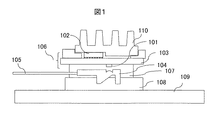
本発明の実施例1を、図1を用いて説明する。実施例1は、光信号を発信または受信する光素子と、電気信号を光信号に変換するために光素子を駆動し、または、光信号から変換された電気信号を増幅する電子回路とが電気配線用基板に搭載された光サブアセンブリと、前記光素子と光信号を伝送する光伝送体を光学的に結合可能とする光コネクタと、前記電気配線用基板と装置ボードとを電気的に結合可能とする電気コネクタから構成される光電気変換モジュールにおいて、前記光コネクタは、前記光サブアセンブリの前記装置ボードと向い合う面に設置され、前記光サブアセンブリの前記装置ボードと向かい合う面に設置される前記電気コネクタは、前記光サブアセンブリの少なくとも向い合う二辺に前記光伝送体を通すことができるように光伝送体が通る少なくとも二辺が開放されており、前記光伝送体を前記光アセンブリと前記装置ボード間に上下に重ねて通すことができるように構成した光電気変換モジュールの実施例である。 A first embodiment of the present invention will be described with reference to FIG. In the first embodiment, an optical element that transmits or receives an optical signal and an electronic circuit that drives the optical element to convert the electrical signal into an optical signal or amplifies the electrical signal converted from the optical signal are electrically connected. An optical subassembly mounted on a wiring board, an optical connector capable of optically coupling the optical element and an optical transmission body that transmits an optical signal, and the electrical wiring board and an apparatus board are electrically coupled. In the photoelectric conversion module including the electrical connector to be enabled, the optical connector is installed on a surface of the optical subassembly facing the device board, and is installed on a surface of the optical subassembly facing the device board. The electrical connector is open on at least two sides through which the optical transmission body passes so that the optical transmission body can pass through at least two opposite sides of the optical subassembly. Cage, is an example of a photoelectric conversion module configured to be able to pass through the optical transmission body one above between the device boards and the light assembly.
図1において、光素子(発光素子または受光素子)101と電子回路102(発光素子駆動回路または電気信号増幅回路)を、電気配線用基板103にフリップチップ搭載する。電気配線用基板103は、ガラス入りエポキシなどの有機またはアルミナなどのセラミック、或いは発光素子からの光を透過させる材料からできている。この中で、光透過性材料としては、例えば、光の波長850nmの場合、電気配線用基板103の材料としてSiが用いられる。光素子である発光素子と受光素子の材料として、GaAsまたはInP系化合物半導体またはSi、Ge半導体などが適用できる。電子回路の材料としては、SiまたはSiGeなどが適用できる。電気配線用基板103の電子回路102を搭載した面と反対側の面にリボン光ファイバ105付き光コネクタ104を搭載する。光コネクタ104は、光路を90度変換する反射器とレンズをモノリシックに集積化した構造を備えている。これにより、光ファイバ105と光素子101との光結合を可能にする。光コネクタ104の材料は、ウルテムなどの樹脂またはガラスでもよい。また、光ファイバ105はポリマーなどからできた光導波路でもよい。電気コネクタ107は一次元配列型のインライン型コネクタで、電気配線用基板103に接続されている。
In FIG. 1, an optical element (light emitting element or light receiving element) 101 and an electronic circuit 102 (light emitting element driving circuit or electric signal amplifier circuit) are flip-chip mounted on an
電気コネクタ107を伝送装置内の装置ボード109に設置されている電気コネクタ用ソケット108に挿入することにより、リボン光ファイバ105付き光コネクタ104が搭載された光サブアセンブリ106(光サブアセンブリ106は光素子101、電子回路102、電気配線用基板103から構成される)を、装置ボード109上に設置する。この場合、光コネクタ104は電気配線用基板103の装置ボードと向い合う面上に搭載されおり、光ファイバ105は光サブアセンブリ106と装置ボード109の間を通る。光素子101と電子回路102を搭載している光サブアセンブリ106の面上には、放熱器110が搭載されている。放熱器110の材料としては、熱伝導性がよく、熱膨張率の小さいタングステン、モリブデンの単体と、タングステン、モリブデンと銅との複合材料及びアルミシリコンカーバイト、窒化アルミニウムセラミックスの複合材料などが適用できる。図1に示す本実施例の光電気変換モジュール構成によれば、光コネクタの設置部分が障害になること無く、放熱が必要な電子回路に大きな放熱器を載置する事ができ、光モジュールの小型化を保ちつつ高効率に放熱が可能となる。
By inserting the
図2に、本発明の実施例2である光電気変換モジュールの断面図を示す。実施例2は、光サブアセンブリ構造が実施例1とは異なるものである。
本例では、少なくとも2チャンネル以上(ここでは4チャンネル)の発光素子101aアレイまたは受光素子101bアレイの一方、または両方を、電気配線用基板103の装置ボード109側の面に搭載する。ここで、発光素子101aの発光面ならびに受光素子101bの受光面のそれぞれと反対側の面が電気配線用基板103の面に接するように搭載する。一方、少なくとも2チャンネル以上のアレイチャンネルが集積された発光素子駆動回路102aまたは電気信号増幅回路102bは、電気配線用基板103の装置ボード側とは反対側の面にフリップチップ搭載する。また、図2のように電気配線用基板103内の光素子と電子回路間にビア200が設けられている。上記の手順で発光素子101aアレイまたは受光素子101bアレイを載置した後、光素子とビア200をワイヤボンディングすることにより、光素子と電子回路が電気配線用基板103を介して電気的に接続される。また、電気コネクタ107と電気配線用基板103は電極パッド201を介して接続されている。同様に、電気コネクタ用ソケット108と装置ボード109も電極パッド201を介して接続されており、光サブアセンブリの電気コネクタ107を電気コネクタ用ソケット108に取付けることにより、光素子および電子回路と装置ボード109間で電気的接続がなされる。
FIG. 2 is a cross-sectional view of the photoelectric conversion module that is Embodiment 2 of the present invention. The second embodiment is different from the first embodiment in the optical subassembly structure.
In this example, one or both of the
光コネクタ104は、電気配線用基板103の装置ボード側の面上にスペーサ202を挿入して、その上に搭載する。スペーサ202の代わりに、電気配線用基板103上に段差を設けて、その上に光コネクタを搭載してもよい。また、光コネクタ104は、12チャンネルのリボン光ファイバ105が載置されたアレイ光コネクタとしている。本例では発光素子101aアレイおよび受光素子101bアレイのそれぞれと、1つのリボン光ファイバ105が光学的に接続されるように構成している。
The
本実施例では、実施例1と同様に、光コネクタの設置部分が障害になること無く、放熱器を介して電子回路を高効率に放熱することができる。さらに、本例では、光コネクタ105に近接して光素子を配置することができるとともに、発光素子101aアレイおよび受光素子101bアレイのそれぞれと、1つのリボン光ファイバ105とを一括して光接続可能のため、部品数や工程数の増大を抑えつつ、光素子と光ファイバとの高効率な光接続が実現できる。
In the present embodiment, similarly to the first embodiment, the electronic circuit can be radiated with high efficiency through the radiator without the obstacle of the installation portion of the optical connector. Further, in this example, optical elements can be arranged close to the
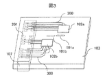
図3に、本発明の実施例3である光電気変換モジュールの上面斜視図を示す。
図3のように、電気配線用基板103の装置ボード側とは反対側の面に発光素子駆動回路102aおよび電気信号増幅回路102bをそれぞれ載置している。また、電気配線用基板103の装置ボード201側の面には発光素子101aならびに受光素子101bを載置し、光素子と電子回路が電気配線用基板103を介して電気的に接続される。ここで、本実施例では発光素子駆動回路102aおよび電気信号増幅回路102bは発光素子101aの発光部ならびに受光素子101bの受光部をそれぞれ結ぶ一直線を中心として互いに向かい合うように載置する。本構成により、発光素子駆動回路102aおよび電気信号増幅回路102bのそれぞれから基板端に載置された電気コネクタ107の電極パッド201まで電気配線300を引き回しする際に、電子回路を横並びに配置するのに対して、駆動回路102aおよび電気信号増幅回路102bの電気配線300間におけるクロストークの抑制と、電子回路の熱分布および配線レイアウトの分散が可能となり、小型化を保ちつつ放熱および高周波特性に優れた光電気変換モジュールを実現できる。
FIG. 3 is a top perspective view of the photoelectric conversion module that is
As shown in FIG. 3, the light emitting
図4に、本発明の実施例4である光電気変換モジュールの断面図を示す。図4のように、光素子と電子回路を搭載している光サブアセンブリ106の面上には、放熱器110が搭載されている。本例では、電気配線用基板103面上の電子回路と電気コネクタ107とを結ぶ電気配線とは反対方向に、発光素子駆動回路102aと接地(GND)とが電気的に接続された金属パタン400aを形成しており、該金属パタン400aと放熱器110が接触した構造としている。同様に、電気信号増幅回路102bと接地(GND)とが電気的に接続された金属パタン400bがビア200を介して電気配線用基板103の内層を通り、再度ビア200を介して金属パタン400aと電気的に接続している。
FIG. 4 shows a cross-sectional view of a photoelectric conversion module that is Embodiment 4 of the present invention. As shown in FIG. 4, a
上記のように、電気配線用基板103面上の電子回路と電気コネクタとを結ぶ電気配線とは反対方向の信号配線パタンの無い広領域にて金属パタン400a、400bと放熱器110とを接触した構造とすることにより、電子回路、または光素子の電気配線用基板103側からの放熱パス確保と、基板実装強度の補強ができる。
As described above, the
図5に、本発明の実施例5である光電気変換モジュールの断面図を示す。本例では図5のように、電気配線用基板103の装置ボード109と向い合う面上に発光素子101aアレイが載置され、該電気配線用基板103の装置ボード109と向い合う面とは反対側の面上に受光素子101bアレイが載置されている。また、図5の下部に、発光素子101aアレイおよび受光素子101bアレイと、リボン光ファイバ105との光結合部の拡大図を示す。拡大図のように、発光素子101aアレイおよび受光素子101bアレイと、光ファイバ105アレイとは光コネクタ104に設けられたレンズ501を介して光学的に接続されている。また、リボン光ファイバ105からの出射光線502は、レンズ501と電気配線用基板103に設けた光スルーホールビア500を介して受光素子101bアレイに導入される。さらに、発光素子101aアレイは光源素子アレイとして一般的に用いられる面発光レーザ(VCSEL)素子を用いている。
FIG. 5 shows a cross-sectional view of a photoelectric conversion module that is Embodiment 5 of the present invention. In this example, as shown in FIG. 5, the
ここで、光ファイバからの出射光線502の開口数(NA)は通常0.2程度であるのに対して、発光素子101aであるVCSELからの出射光線503の開口数は0.3〜0.4程度と大きい。そのため、電気配線用基板103と同一面上に発光素子101aと受光素子101bを配置すると、リボン光ファイバ105とそれぞれの光素子間の光学距離がほぼ同じとなり、上記光ファイバと発光素子との開口数の差、すなわちビーム拡がり角の差によって高効率な光結合効率の確保が困難となる。そこで、本例のように、光ファイバに対して開口数の大きい発光素子101aのVCSELを電気配線用基板103の光コネクタ104と近い面に載置し、それと反対側の面上に受光素子101bを載置することによって、上記光素子および光ファイバの開口数(NA)の差による光結合効率の劣化を抑制することができる。また、本構成によって、光コネクタ104に設けられたレンズ501は送信部および受信部共に同じ形状のレンズアレイも用いることが可能となり、部品数や組立工程数の削減にも有効である。
Here, the numerical aperture (NA) of the
本発明の実施例6は、光電気変換モジュールを複数配置したものである。
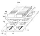
図6に、本発明の実施例1の光電気変換モジュールを下側から見た図を示す。電気コネクタ107は、その長手方向とリボン光ファイバ105が略平行になるように設置する。電気コネクタ107は一次元配列であり、光サブアセンブリの向かい合う二辺を含む三辺が開放されているので、図7に示すように、本光電気変換モジュールを2次元配置し、光ファイバ105を配線することができ、装置ボード109上に高密度実装することが可能となる。さらに、装置ボード109と反対側の光サブアセンブリの上面には光コネクタならびに光ファイバがないため、図8に示すように、取り付が容易でかつ放熱効率が高い一括型放熱器800を設置することができる。ここで、一括型放熱器800は、水冷型または空冷型のどちらでもよい。図6に示した電気コネクタを1つ設置する形式に代えて、図9に示すように、電気コネクタ107をもう一つ、光コネクタ104を挟んで電気配線用基板103同一面の反対側に設置した形式としてもよい。図9の変形例においても、光サブアセンブリの向かい合う二辺(電気コネクタの長軸方向と交差する二辺)が開放されているので、隣の光電気変換モジュールからのリボンファイバを通すことができ、図7に示すような、光電気変換モジュールの二次元配列が可能である。
In Example 6 of the present invention, a plurality of photoelectric conversion modules are arranged.
FIG. 6 shows a view of the photoelectric conversion module according to the first embodiment of the present invention as viewed from below. The
図10に、実施例7の光電気変換モジュールを示す。実施例7は、電気コネクタの構造が実施例1とは異なるものであり、図10は、電気コネクタを裏側から見た図である。 In FIG. 10, the photoelectric conversion module of Example 7 is shown. The seventh embodiment is different from the first embodiment in the structure of the electrical connector, and FIG. 10 is a view of the electrical connector as viewed from the back side.
電気コネクタとして、電気パッドが二次元配列している電気コネクタ1001を用いる。電気コネクタ1001は、光コネクタ104の周囲を取り囲む構造をしている。電気コネクタ1001は、リボン光ファイバ105と隣の光電気変換モジュールのリボンファイバが通れるように、向かい合う二つの辺に第一の窓領域1002と第二の窓領域1003の二つの窓領域を有する。これにより、光電気変換モジュールを図7のように二次元配列できる。
As the electrical connector, an electrical connector 1001 in which electrical pads are two-dimensionally arranged is used. The electrical connector 1001 has a structure surrounding the
本実施例では、実施例1で説明した電気パッドが一次元配列している電気コネクタ107に比べて、配線数が多くとれるメリットがある。
This embodiment has an advantage that the number of wirings can be increased as compared with the
図11に、実施例8の光電気変換モジュールを示す。実施例8は、装置ボード上に設置された電気コネクタのソケットと当該電気コネクタのソケットに固定された光コネクタに、電気コネクタと光コネクタを一括して接続することが可能な、光サブアセンブリに電気コネクタと光コネクタのソケットが搭載された光電気変換モジュールの実施例である。 In FIG. 11, the photoelectric conversion module of Example 8 is shown. Example 8 is an optical subassembly capable of collectively connecting an electrical connector and an optical connector to an electrical connector socket installed on the device board and an optical connector fixed to the electrical connector socket. It is the Example of the photoelectric conversion module with which the socket of the electrical connector and the optical connector was mounted.
電気コネクタ用のソケット108に、接着固定またはガイドピンなどを用いて勘合して固定された光コネクタ1101を装置ボード109上に取り付ける。その後、電気コネクタ107と光コネクタ用ソケット1102が搭載された光サブアセンブリ106を、電気コネクタ107と電気コネクタ用ソケット108を、かつ光コネクタ1101と光コネクタ用ソケット1102をそれぞれ位置合せして、電気コネクタと光コネクタを一括して嵌めこむ。光コネクタ1101と光コネクタ用ソケット1102はガイドピン1103によって勘合する。
An
この実施例により、光電気変換モジュールの装置ボード上への搭載工程数が減り、作業が容易になる。 According to this embodiment, the number of steps of mounting the photoelectric conversion module on the device board is reduced, and the operation is facilitated.
図12および図13に、実施例9の光電気変換モジュールを示す。図12は、光ファイバの高さを容易に変えることができる光コネクタと光コネクタ用ソケットの説明図、図13は、図12の光コネクタと光コネクタ用ソケットを搭載した光電気変換モジュールを配列した場合の断面図である。実施例9は、光素子と光伝送体との光結合を可能にする光接続部が、第一レンズ用レンズホルダーを有する光コネクタ用ソケットと、第二レンズと光路方向変換ミラーを有する光コネクタから構成されており、前記第二レンズから出射または当該第二レンズに入射する光は略平行光である光電気変換モジュールの実施例である。
12 and 13 show the photoelectric conversion module of Example 9. FIG. FIG. 12 is an explanatory diagram of an optical connector and an optical connector socket that can easily change the height of the optical fiber, and FIG. 13 is an array of photoelectric conversion modules equipped with the optical connector and optical connector socket of FIG. FIG.
光コネクタ用ソケット1202は、第一レンズ1201用レンズホルダー1203とガイドピン1103から構成されている。光コネクタ104は第二レンズ1200、光路方向変換ミラー、光ファイバ搭載用V溝構造から構成されている。このV溝構造に代えて、光ファイバが通る穴でもよい。光素子101側の第一レンズは光を集光して光素子との高い光結合効率を実現する。一方、光コネクタ104の第二レンズから出射または第二レンズに入射する光は略平行光となるように、第二レンズを設計する。この場合、第一レンズ1201と第二レンズ1200との間の距離を大きく変えても、光素子との光結合効率の変化は小さくなると期待できる。その結果、光コネクタ104の厚さを大きく変えることができ、装置ボード上からの光ファイバ105の高さを任意に変えることができる。
The
このような光ファイバ105の高さが異なるような光電気変換モジュールを用いれば、装置ボード109上に光電気変換モジュールを搭載した場合、図13に示すように、隣の光電気変換モジュールの光ファイバに妨げられずに、光ファイバの引き回しが可能となる。光コネクタと装置ボード間の距離を3mm、ファイバ被覆の直径を0.25mmとすると、最大12本分の光ファイバの重ねが可能である。
When such photoelectric conversion modules having different heights of the
図14に、本発明の光電気変換モジュールを用いた伝送装置の実施例を示す。図14は上から見た図である。図14に示す通り、装置ボード109上のLSI1402の周りに本発明の光電気変換モジュール1400を二次元状に配置する。各光電気変換モジュール1400の光ファイバ105はモジュールと装置ボード間を通って引き回されて、バックプレーン光コネクタ1401に接続される。
FIG. 14 shows an embodiment of a transmission apparatus using the photoelectric conversion module of the present invention. FIG. 14 is a view from above. As shown in FIG. 14, the
この方法により、装置ボード間の信号伝送を光信号で行うことにより、信号処理能力の高い伝送装置を実現することが可能となる。 With this method, it is possible to realize a transmission apparatus with high signal processing capability by performing signal transmission between apparatus boards using optical signals.
101 光素子
101a 発光素子
101b 受光素子
102 電子回路
102a 発光素子駆動回路
102b 電気信号増幅回路
103 電気配線用基板
104 光コネクタ
105 リボン光ファイバ
106 光サブアセンブリ
107 電気コネクタ
108 電気コネクタ用ソケット
109 装置ボード
110 放熱器
200 ビア
201 電極パッド
202 スペーサ
300 電気配線
400a、400b 金属パタン
500 光スルーホールビア
501 レンズ
502 光ファイバからの出射光線
503 発光素子からの出射光線
800 一括型放熱器
1001 電気コネクタ
1002 第一の窓領域
1003 第二の窓領域
1101 光コネクタ
1102 光コネクタ用ソケット
1103 ガイドピン
1200 第二レンズ
1201 第一レンズ
1202 光コネクタ用ソケット
1203 レンズホルダー
1400 光電気変換モジュール
1401 バックプレーン光コネクタ
1402 LSI
DESCRIPTION OF
Claims (14)
前記光素子と光信号を伝送する光伝送体を光学的に結合可能とする光コネクタと、
前記電気配線用基板と装置ボードとを電気的に結合可能とする電気コネクタとから構成される光電気変換モジュールにおいて、
前記光コネクタは、前記光サブアセンブリの前記装置ボードと向い合う面に設置され、
前記光サブアセンブリの前記装置ボードと向い合う面に設置される前記電気コネクタは、前記光サブアセンブリの少なくとも向い合う二辺に前記光伝送体を通すことができるように光伝送体が通る少なくとも二辺が開放されており、
前記光伝送体を前記光アセンブリと前記装置ボード間に上下に重ねて通すことができるように構成した光電気変換モジュール。 An optical circuit that transmits or receives an optical signal and an electronic circuit that drives the optical element to convert the electrical signal into an optical signal or amplifies the electrical signal converted from the optical signal are mounted on the electrical wiring board. An optical subassembly,
An optical connector capable of optically coupling the optical element and an optical transmission body for transmitting an optical signal;
In the photoelectric conversion module composed of an electrical connector capable of electrically coupling the electrical wiring board and the device board,
The optical connector is installed on a surface of the optical subassembly facing the device board;
The electrical connector installed on the surface of the optical subassembly facing the device board is at least two through which the optical transmission body passes so that the optical transmission body can be passed through at least two opposite sides of the optical subassembly. The sides are open,
A photoelectric conversion module configured to allow the optical transmission body to pass vertically between the optical assembly and the device board.
少なくとも2チャンネルの前記電子回路が、前記電気配線用基板の、前記装置ボードと向い合う面とは反対側の面上に載置され、少なくとも2チャンネルの、光信号を発信または受信する前記光素子のうち少なくとも一方が、前記電気配線用基板の電子回路搭載面とは別の面に載置されている光電気変換モジュール。 The photoelectric conversion module according to claim 1,
The optical element on which the electronic circuit of at least two channels is mounted on the surface of the electrical wiring board opposite to the surface facing the device board, and transmits or receives at least two channels of optical signals. The photoelectric conversion module in which at least one is mounted in the surface different from the electronic circuit mounting surface of the said board | substrate for electrical wiring.
光信号を発信または受信する前記光素子は、それぞれ少なくとも2チャンネル以上のアレイ光素子であり、前記光コネクタは、少なくとも4チャンネル以上の前記光伝送体が載置されたアレイ光コネクタであり、前記少なくとも1つの発光または受光素子アレイと、前記1つの光ファイバアレイが光学的に接続されるように構成された光電気変換モジュール。 The photoelectric conversion module according to claim 1,
The optical elements that transmit or receive optical signals are each an array optical element having at least two channels, and the optical connector is an array optical connector on which the optical transmission body having at least four channels is mounted, An optoelectric conversion module configured to optically connect at least one light emitting or light receiving element array and the one optical fiber array.
前記電気配線用基板に載置された前記電子回路のうち、電気信号を光信号に変換するために光素子を駆動する電子回路と、光信号から変換された電気信号を増幅する電子回路とが、少なくとも2つの前記光素子の、発光または受光部をそれぞれ結ぶ一直線を中心として互いに向かい合うように載置されている光電気変換モジュール。 The photoelectric conversion module according to claim 2,
Of the electronic circuits mounted on the electrical wiring board, an electronic circuit that drives an optical element to convert an electrical signal into an optical signal, and an electronic circuit that amplifies the electrical signal converted from the optical signal The photoelectric conversion module placed so as to face each other around a straight line connecting the light emitting or light receiving portions of at least two of the optical elements.
前記電子回路が搭載された前記電気配線用基板と同一面上に、前記電子回路を放熱するための放熱器が載置され、前記電気配線用基板面上で、前記電子回路および接地と電気的に接続された金属パタンが形成され、前記放熱器と前記金属パタンとが接触されている光電気変換モジュール。 The photoelectric conversion module according to claim 2,
A radiator for dissipating heat from the electronic circuit is placed on the same surface as the electric wiring board on which the electronic circuit is mounted. The electronic circuit and the ground are electrically connected to the electric wiring board surface. A photoelectric conversion module in which a metal pattern connected to the heat sink is formed, and the radiator and the metal pattern are in contact with each other.
前記電気配線用基板の装置ボードと向い合う面上に発光素子アレイが載置され、前記電気配線用基板の装置ボードと向い合う面とは反対側の面上に受光素子アレイが載置されている光電気変換モジュール。 In the photoelectric conversion module according to claim 3,
A light emitting element array is placed on the surface of the electrical wiring board facing the device board, and a light receiving element array is placed on the surface opposite to the face of the electrical wiring board facing the device board. Photoelectric conversion module.
前記電気コネクタが、前記光伝送体と略平行となるように、前記光サブアセンブリの一辺に配置されている光電気変換モジュール。 The photoelectric conversion module according to claim 1,
The photoelectric conversion module arranged on one side of the optical subassembly so that the electrical connector is substantially parallel to the optical transmission body.
前記電気コネクタが、前記光伝送体と略平行となるように、前記光サブアセンブリの向かい合う二辺に配置されている光電気変換モジュール。 The photoelectric conversion module according to claim 1,
The photoelectric conversion module which is arrange | positioned at the two opposite sides of the said optical subassembly so that the said electrical connector may become substantially parallel to the said optical transmission body.
前記電気コネクタが、前記光コネクタの周囲を取り囲む構造であり、少なくとも向かい合う二つの辺に、前記光伝送体を通すための少なくとも二つの窓領域を有する光電気変換モジュール。 The photoelectric conversion module according to claim 1,
The electrical connector has a structure that surrounds the periphery of the optical connector, and has at least two window regions for passing the optical transmission body on at least two sides facing each other.
前記電気コネクタは、電気パッドが二次元配列している光電気変換モジュール。 The photoelectric conversion module according to claim 9, wherein
The electrical connector is a photoelectric conversion module in which electrical pads are two-dimensionally arranged.
前記装置ボード上に電気コネクタのソケットを設置するとともに、当該電気コネクタのソケットに光コネクタを固定し、前記光サブアセンブリに電気コネクタと光コネクタのソケットを搭載し、前記電気コネクタと前記光コネクタを一括して接続することを可能とした光電気変換モジュール。 The photoelectric conversion module according to claim 1,
An electrical connector socket is installed on the device board, an optical connector is fixed to the electrical connector socket, an electrical connector and an optical connector socket are mounted on the optical subassembly, and the electrical connector and the optical connector are mounted. A photoelectric conversion module that can be connected together.
前記光素子と前記光伝送体との光結合を可能にする光接続部が、第一レンズと、当該第一レンズを収納するレンズホルダーを有する光コネクタ用ソケットと、第二レンズと光方向変換ミラーを有する光コネクタから構成されており、前記第二レンズから出射または当該第二レンズに入射する光が略平行光である光電気変換モジュール。 The photoelectric conversion module according to claim 1,
An optical connecting portion that enables optical coupling between the optical element and the optical transmission body includes a first lens, an optical connector socket having a lens holder that houses the first lens, a second lens, and an optical direction change. An opto-electric conversion module that includes an optical connector having a mirror, and that the light emitted from or incident on the second lens is substantially parallel light.
複数の光電気変換モジュールの間で、前記光コネクタの厚さを変化させた光電気変換モジュール。 The photoelectric conversion module according to claim 12, wherein
A photoelectric conversion module in which a thickness of the optical connector is changed among a plurality of photoelectric conversion modules.
Priority Applications (3)
| Application Number | Priority Date | Filing Date | Title |
|---|---|---|---|
| JP2013211345A JP2015076489A (en) | 2013-10-08 | 2013-10-08 | Photoelectric conversion module and transmission device using the same |
| US14/508,418 US9217835B2 (en) | 2013-10-08 | 2014-10-07 | Photoelectric conversion module and transmission apparatus using the same |
| CN201410524376.2A CN104516066B (en) | 2013-10-08 | 2014-10-08 | Light-to-current inversion module and use its transmitting device |
Applications Claiming Priority (1)
| Application Number | Priority Date | Filing Date | Title |
|---|---|---|---|
| JP2013211345A JP2015076489A (en) | 2013-10-08 | 2013-10-08 | Photoelectric conversion module and transmission device using the same |
Publications (2)
| Publication Number | Publication Date |
|---|---|
| JP2015076489A true JP2015076489A (en) | 2015-04-20 |
| JP2015076489A5 JP2015076489A5 (en) | 2016-08-25 |
Family
ID=52777016
Family Applications (1)
| Application Number | Title | Priority Date | Filing Date |
|---|---|---|---|
| JP2013211345A Pending JP2015076489A (en) | 2013-10-08 | 2013-10-08 | Photoelectric conversion module and transmission device using the same |
Country Status (2)
| Country | Link |
|---|---|
| US (1) | US9217835B2 (en) |
| JP (1) | JP2015076489A (en) |
Cited By (2)
| Publication number | Priority date | Publication date | Assignee | Title |
|---|---|---|---|---|
| JP2016156916A (en) * | 2015-02-24 | 2016-09-01 | 住友電気工業株式会社 | Optical data link |
| JP2020177192A (en) * | 2019-04-22 | 2020-10-29 | 住友電気工業株式会社 | Optical transceiver |
Families Citing this family (10)
| Publication number | Priority date | Publication date | Assignee | Title |
|---|---|---|---|---|
| US9285555B2 (en) * | 2010-11-25 | 2016-03-15 | Gnitabouré YABRE | Optical circuit board |
| US9350448B2 (en) * | 2013-12-03 | 2016-05-24 | Cisco Technology, Inc. | Multi-beam free space optical endpoint |
| TWI617852B (en) * | 2014-10-16 | 2018-03-11 | 英屬開曼群島商鴻騰精密科技股份有限公司 | Optical module |
| JP2016197635A (en) * | 2015-04-02 | 2016-11-24 | 日立金属株式会社 | Transmitter-receiver integrated optical subassembly and optical module |
| US10877217B2 (en) | 2017-01-06 | 2020-12-29 | Rockley Photonics Limited | Copackaging of asic and silicon photonics |
| US10761262B2 (en) * | 2017-08-01 | 2020-09-01 | Rockley Photonics Limited | Module with transmit and receive optical subassemblies with specific pic cooling architecture |
| JP7117133B2 (en) * | 2018-04-16 | 2022-08-12 | 日本ルメンタム株式会社 | Optical subassembly, manufacturing method thereof, and optical module |
| JP7243449B2 (en) * | 2019-05-24 | 2023-03-22 | 富士通オプティカルコンポーネンツ株式会社 | optical module |
| US20210356683A1 (en) * | 2020-05-13 | 2021-11-18 | Hisense Broadband Multimedia Technologies Co., Ltd. | Optical module |
| JP2022124177A (en) * | 2021-02-15 | 2022-08-25 | 株式会社日本マイクロニクス | Connection device and light condensing substrate |
Citations (5)
| Publication number | Priority date | Publication date | Assignee | Title |
|---|---|---|---|---|
| JP2006126370A (en) * | 2004-10-27 | 2006-05-18 | Sony Corp | Composite photoelectric device, ic socket and optical waveguide used for the device and electronic appliance using the device |
| JP2006133763A (en) * | 2004-10-07 | 2006-05-25 | Nec Corp | Structure and method of mounting lsi package to photoelectric wiring board, information processing apparatus, optical interface and photoelectric wiring board |
| JP2006235115A (en) * | 2005-02-23 | 2006-09-07 | Sony Corp | Optical signal inputting device and electronic equipment using it |
| US20080298818A1 (en) * | 2007-03-05 | 2008-12-04 | Aprius, Inc. | Optical Receiver for Computing Applications |
| JP2010062087A (en) * | 2008-09-05 | 2010-03-18 | Hitachi Ltd | Optoelectrical module |
Family Cites Families (1)
| Publication number | Priority date | Publication date | Assignee | Title |
|---|---|---|---|---|
| EP2428828B1 (en) | 2010-09-13 | 2016-06-29 | Tyco Electronics Svenska Holdings AB | Miniaturized high speed optical module |
-
2013
- 2013-10-08 JP JP2013211345A patent/JP2015076489A/en active Pending
-
2014
- 2014-10-07 US US14/508,418 patent/US9217835B2/en not_active Expired - Fee Related
Patent Citations (5)
| Publication number | Priority date | Publication date | Assignee | Title |
|---|---|---|---|---|
| JP2006133763A (en) * | 2004-10-07 | 2006-05-25 | Nec Corp | Structure and method of mounting lsi package to photoelectric wiring board, information processing apparatus, optical interface and photoelectric wiring board |
| JP2006126370A (en) * | 2004-10-27 | 2006-05-18 | Sony Corp | Composite photoelectric device, ic socket and optical waveguide used for the device and electronic appliance using the device |
| JP2006235115A (en) * | 2005-02-23 | 2006-09-07 | Sony Corp | Optical signal inputting device and electronic equipment using it |
| US20080298818A1 (en) * | 2007-03-05 | 2008-12-04 | Aprius, Inc. | Optical Receiver for Computing Applications |
| JP2010062087A (en) * | 2008-09-05 | 2010-03-18 | Hitachi Ltd | Optoelectrical module |
Cited By (2)
| Publication number | Priority date | Publication date | Assignee | Title |
|---|---|---|---|---|
| JP2016156916A (en) * | 2015-02-24 | 2016-09-01 | 住友電気工業株式会社 | Optical data link |
| JP2020177192A (en) * | 2019-04-22 | 2020-10-29 | 住友電気工業株式会社 | Optical transceiver |
Also Published As
| Publication number | Publication date |
|---|---|
| US9217835B2 (en) | 2015-12-22 |
| US20150098675A1 (en) | 2015-04-09 |
| CN104516066A (en) | 2015-04-15 |
Similar Documents
| Publication | Publication Date | Title |
|---|---|---|
| JP2015076489A (en) | Photoelectric conversion module and transmission device using the same | |
| CN107040318B (en) | Method and system for communication | |
| US11863917B2 (en) | Assembly of network switch ASIC with optical transceivers | |
| US10962728B2 (en) | Co-packaged optics and transceiver | |
| EP3121630B1 (en) | Optoelectronic module with improved heat management | |
| US9647762B2 (en) | Integrated parallel optical transceiver | |
| US6955481B2 (en) | Method and apparatus for providing parallel optoelectronic communication with an electronic device | |
| JP6294838B2 (en) | Chip assembly configuration with densely packed optical interconnects | |
| US10483413B2 (en) | Photoelectric module and optical device | |
| JP5708816B2 (en) | Optical module | |
| KR100460703B1 (en) | Electro-optical circuit board having unified optical transmission/receiving module and optical waveguide | |
| JP2007271998A (en) | Optical connector and optical module | |
| US6685364B1 (en) | Enhanced folded flexible cable packaging for use in optical transceivers | |
| KR20100092861A (en) | Optoelectric complex wring module and manufacturing method thereof | |
| JP2007293018A (en) | Optoelectric composite module and optical i/o apparatus | |
| JPWO2006035499A1 (en) | Opto-electric integrated circuit element and transmission device using the same | |
| US6786651B2 (en) | Optical interconnect structure, system and transceiver including the structure, and method of forming the same | |
| US8348522B2 (en) | Attachable components for providing an optical interconnect between/through printed wiring boards | |
| JP2008041772A (en) | Optical module | |
| JP2012013726A (en) | Optical interconnection module, and optical and electrical circuit board using the same | |
| WO2015132849A1 (en) | Photoelectric conversion module and information device using same | |
| JP2012141471A (en) | Optical interconnection module | |
| JPWO2009001822A1 (en) | Optical module | |
| JP2012128387A (en) | Optical waveguide device and optical transmission device using the same | |
| JP6260167B2 (en) | Photoelectric fusion module |
Legal Events
| Date | Code | Title | Description |
|---|---|---|---|
| A521 | Request for written amendment filed |
Free format text: JAPANESE INTERMEDIATE CODE: A523 Effective date: 20160711 |
|
| A621 | Written request for application examination |
Free format text: JAPANESE INTERMEDIATE CODE: A621 Effective date: 20160711 |
|
| A977 | Report on retrieval |
Free format text: JAPANESE INTERMEDIATE CODE: A971007 Effective date: 20170405 |
|
| A131 | Notification of reasons for refusal |
Free format text: JAPANESE INTERMEDIATE CODE: A131 Effective date: 20170411 |
|
| A02 | Decision of refusal |
Free format text: JAPANESE INTERMEDIATE CODE: A02 Effective date: 20171017 |