JP2015047692A - Method of chemical mechanical polishing substrate - Google Patents
Method of chemical mechanical polishing substrate Download PDFInfo
- Publication number
- JP2015047692A JP2015047692A JP2014174665A JP2014174665A JP2015047692A JP 2015047692 A JP2015047692 A JP 2015047692A JP 2014174665 A JP2014174665 A JP 2014174665A JP 2014174665 A JP2014174665 A JP 2014174665A JP 2015047692 A JP2015047692 A JP 2015047692A
- Authority
- JP
- Japan
- Prior art keywords
- layer
- polishing
- substrate
- chemical mechanical
- mechanical polishing
- Prior art date
- Legal status (The legal status is an assumption and is not a legal conclusion. Google has not performed a legal analysis and makes no representation as to the accuracy of the status listed.)
- Pending
Links
Images


Classifications
-
- B—PERFORMING OPERATIONS; TRANSPORTING
- B24—GRINDING; POLISHING
- B24B—MACHINES, DEVICES, OR PROCESSES FOR GRINDING OR POLISHING; DRESSING OR CONDITIONING OF ABRADING SURFACES; FEEDING OF GRINDING, POLISHING, OR LAPPING AGENTS
- B24B37/00—Lapping machines or devices; Accessories
- B24B37/11—Lapping tools
- B24B37/20—Lapping pads for working plane surfaces
- B24B37/24—Lapping pads for working plane surfaces characterised by the composition or properties of the pad materials
-
- B—PERFORMING OPERATIONS; TRANSPORTING
- B24—GRINDING; POLISHING
- B24B—MACHINES, DEVICES, OR PROCESSES FOR GRINDING OR POLISHING; DRESSING OR CONDITIONING OF ABRADING SURFACES; FEEDING OF GRINDING, POLISHING, OR LAPPING AGENTS
- B24B1/00—Processes of grinding or polishing; Use of auxiliary equipment in connection with such processes
-
- B—PERFORMING OPERATIONS; TRANSPORTING
- B24—GRINDING; POLISHING
- B24B—MACHINES, DEVICES, OR PROCESSES FOR GRINDING OR POLISHING; DRESSING OR CONDITIONING OF ABRADING SURFACES; FEEDING OF GRINDING, POLISHING, OR LAPPING AGENTS
- B24B37/00—Lapping machines or devices; Accessories
- B24B37/11—Lapping tools
- B24B37/20—Lapping pads for working plane surfaces
- B24B37/205—Lapping pads for working plane surfaces provided with a window for inspecting the surface of the work being lapped
-
- B—PERFORMING OPERATIONS; TRANSPORTING
- B24—GRINDING; POLISHING
- B24B—MACHINES, DEVICES, OR PROCESSES FOR GRINDING OR POLISHING; DRESSING OR CONDITIONING OF ABRADING SURFACES; FEEDING OF GRINDING, POLISHING, OR LAPPING AGENTS
- B24B37/00—Lapping machines or devices; Accessories
- B24B37/11—Lapping tools
- B24B37/20—Lapping pads for working plane surfaces
- B24B37/22—Lapping pads for working plane surfaces characterised by a multi-layered structure
-
- C—CHEMISTRY; METALLURGY
- C08—ORGANIC MACROMOLECULAR COMPOUNDS; THEIR PREPARATION OR CHEMICAL WORKING-UP; COMPOSITIONS BASED THEREON
- C08G—MACROMOLECULAR COMPOUNDS OBTAINED OTHERWISE THAN BY REACTIONS ONLY INVOLVING UNSATURATED CARBON-TO-CARBON BONDS
- C08G18/00—Polymeric products of isocyanates or isothiocyanates
- C08G18/06—Polymeric products of isocyanates or isothiocyanates with compounds having active hydrogen
- C08G18/08—Processes
- C08G18/10—Prepolymer processes involving reaction of isocyanates or isothiocyanates with compounds having active hydrogen in a first reaction step
-
- H—ELECTRICITY
- H01—ELECTRIC ELEMENTS
- H01L—SEMICONDUCTOR DEVICES NOT COVERED BY CLASS H10
- H01L21/00—Processes or apparatus adapted for the manufacture or treatment of semiconductor or solid state devices or of parts thereof
- H01L21/02—Manufacture or treatment of semiconductor devices or of parts thereof
- H01L21/04—Manufacture or treatment of semiconductor devices or of parts thereof the devices having at least one potential-jump barrier or surface barrier, e.g. PN junction, depletion layer or carrier concentration layer
- H01L21/18—Manufacture or treatment of semiconductor devices or of parts thereof the devices having at least one potential-jump barrier or surface barrier, e.g. PN junction, depletion layer or carrier concentration layer the devices having semiconductor bodies comprising elements of Group IV of the Periodic System or AIIIBV compounds with or without impurities, e.g. doping materials
- H01L21/30—Treatment of semiconductor bodies using processes or apparatus not provided for in groups H01L21/20 - H01L21/26
- H01L21/302—Treatment of semiconductor bodies using processes or apparatus not provided for in groups H01L21/20 - H01L21/26 to change their surface-physical characteristics or shape, e.g. etching, polishing, cutting
- H01L21/306—Chemical or electrical treatment, e.g. electrolytic etching
- H01L21/30625—With simultaneous mechanical treatment, e.g. mechanico-chemical polishing
-
- H—ELECTRICITY
- H01—ELECTRIC ELEMENTS
- H01L—SEMICONDUCTOR DEVICES NOT COVERED BY CLASS H10
- H01L21/00—Processes or apparatus adapted for the manufacture or treatment of semiconductor or solid state devices or of parts thereof
- H01L21/02—Manufacture or treatment of semiconductor devices or of parts thereof
- H01L21/04—Manufacture or treatment of semiconductor devices or of parts thereof the devices having at least one potential-jump barrier or surface barrier, e.g. PN junction, depletion layer or carrier concentration layer
- H01L21/18—Manufacture or treatment of semiconductor devices or of parts thereof the devices having at least one potential-jump barrier or surface barrier, e.g. PN junction, depletion layer or carrier concentration layer the devices having semiconductor bodies comprising elements of Group IV of the Periodic System or AIIIBV compounds with or without impurities, e.g. doping materials
- H01L21/30—Treatment of semiconductor bodies using processes or apparatus not provided for in groups H01L21/20 - H01L21/26
- H01L21/31—Treatment of semiconductor bodies using processes or apparatus not provided for in groups H01L21/20 - H01L21/26 to form insulating layers thereon, e.g. for masking or by using photolithographic techniques; After treatment of these layers; Selection of materials for these layers
- H01L21/3205—Deposition of non-insulating-, e.g. conductive- or resistive-, layers on insulating layers; After-treatment of these layers
- H01L21/321—After treatment
- H01L21/32115—Planarisation
- H01L21/3212—Planarisation by chemical mechanical polishing [CMP]
Abstract
Description
本発明は、基材を化学機械研磨する方法に関する。より具体的には、本発明は、基材を提供する工程、組成及び研磨面を有する研磨層であって、組成が、初期加水分解安定性を持続的加水分解不安定性と併せて示すように選択されている研磨層と、上面及び下面を有する硬質層と、研磨層のベース面と硬質層の上面との間に挿入された、研磨層を硬質層に接着するホットメルト接着剤と、スタック側及びプラテン側を有する感圧プラテン接着剤層であって、スタック側が硬質層の下面に隣接する感圧接着剤層とを含む化学機械研磨パッドを提供する工程、及び研磨面と基材との間に動的接触を生じさせて基材の表面を研磨する工程を含む、基材を化学機械研磨する方法に関する。 The present invention relates to a method for chemical mechanical polishing a substrate. More specifically, the present invention is a polishing layer having a step of providing a substrate, a composition and a polishing surface, such that the composition exhibits initial hydrolysis stability in combination with persistent hydrolysis instability. A selected polishing layer; a hard layer having an upper surface and a lower surface; a hot melt adhesive inserted between the base surface of the polishing layer and the upper surface of the hard layer; Providing a chemical mechanical polishing pad having a pressure sensitive platen adhesive layer having a side and a platen side, the stack side including a pressure sensitive adhesive layer adjacent to the lower surface of the hard layer; and The present invention relates to a method for chemical mechanical polishing of a substrate, comprising the step of polishing the surface of the substrate by causing dynamic contact therebetween.
半導体の製造は通常、いくつかの化学機械平坦化(CMP)工程を含む。各CMP工程において、研磨パッドが、研磨溶液、たとえば砥粒含有研磨スラリー又は無砥粒反応性液と組み合わさって、後続の層の受け入れに備えて平坦化する、又は平坦さを維持するようなやり方で余剰材料を除去する。これらの層の積み重ねが、集積回路を形成するようなやり方で組み合わさる。これらの半導体素子の製造は、より高い作動速度、より少ない漏れ電流及び低下した電力消費を有する素子に対する要求のせいで、より複雑化し続けている。素子アーキテクチャの点では、これは、より微細な形体幾何学及び増大したメタライゼーションレベルと言い換えることができる。これらのますます厳しくなる素子設計要求が、より低い誘電率を有する新たな絶縁材料とともに銅メタライゼーションの採用を強要している。 Semiconductor manufacturing typically includes several chemical mechanical planarization (CMP) steps. In each CMP step, the polishing pad is combined with a polishing solution, such as an abrasive-containing polishing slurry or an abrasive-free reactive liquid, such that it is planarized or remains flat for subsequent layer acceptance. Remove excess material in a manner. These stacks of layers combine in such a way as to form an integrated circuit. The manufacture of these semiconductor devices continues to become more complex due to the demand for devices with higher operating speeds, lower leakage currents and reduced power consumption. In terms of device architecture, this can be translated into finer feature geometry and increased metallization levels. These increasingly stringent device design requirements force the adoption of copper metallization along with new insulating materials with lower dielectric constants.
化学機械研磨におけるもっとも重大な課題の一つが、半導体ウェーハ上の表面形体の平坦化と、素子収率の低下を招く欠陥形成、特にスクラッチ欠陥の最小限化との間の所望のバランスを達成することである。従来の見識は、平坦化と欠陥とのバランスは、化学機械研磨パッドの研磨層に使用されるポリマー材料の硬さの関数であるということである。すなわち、従来の見識は、より硬い研磨層材料がより高い平坦化をより高い欠陥数とともに提供し、より軟らかい研磨層材料がより低い平坦化をより低い欠陥数とともに提供するということである。化学機械研磨における平坦化と欠陥形成との間のこの折り合いを打ち破る方法を特定することが望ましいであろう。 One of the most critical challenges in chemical mechanical polishing is to achieve the desired balance between planarization of surface features on semiconductor wafers and defect formation that leads to reduced device yields, especially minimizing scratch defects That is. The conventional wisdom is that the balance between planarization and defects is a function of the hardness of the polymer material used in the polishing layer of the chemical mechanical polishing pad. That is, the conventional insight is that a harder polishing layer material provides higher planarization with a higher number of defects, and a softer polishing layer material provides lower planarization with a lower number of defects. It would be desirable to identify a way to overcome this compromise between planarization and defect formation in chemical mechanical polishing.
化学機械研磨法においては、通常、水性研磨溶液が、研磨層の研磨面と研磨される基材の表面との間に挿入される。したがって、従来の見識は、化学機械研磨に使用される研磨層材料は、水に長期間暴露されたときでも加水分解安定性を維持すべきであるということである。 In chemical mechanical polishing methods, an aqueous polishing solution is usually inserted between the polishing surface of the polishing layer and the surface of the substrate to be polished. Thus, the conventional insight is that polishing layer materials used for chemical mechanical polishing should maintain hydrolytic stability even when exposed to water for extended periods of time.
ポリウレタン研磨層のファミリーがKulpによって米国特許第8,288,448号に開示されている。Kulpは、プレポリマーポリオールと多官能イソシアネートとのプレポリマー反応から形成されるイソシアネート末端反応生成物で形成されるキャストポリウレタンポリマー材料を含む研磨パッドを開示している。イソシアネート末端反応生成物は4.5〜8.7重量%の未反応NCOを有し、イソシアネート末端反応生成物は、硬化剤ポリアミン、硬化剤ポリオール、硬化剤アルコールアミン及びそれらの混合物からなる群より選択される硬化剤で硬化させられる。 A family of polyurethane polishing layers is disclosed by Kulp in US Pat. No. 8,288,448. Kulp discloses a polishing pad comprising a cast polyurethane polymer material formed with an isocyanate-terminated reaction product formed from a prepolymer reaction of a prepolymer polyol and a polyfunctional isocyanate. The isocyanate-terminated reaction product has 4.5 to 8.7% by weight unreacted NCO, and the isocyanate-terminated reaction product is from the group consisting of a curing agent polyamine, a curing agent polyol, a curing agent alcohol amine, and mixtures thereof. Cured with a selected curing agent.
それにもかかわらず、欠陥形成を最小限にしながらもより高い程度の平坦化を提供する改良された化学機械研磨法の必要性が絶えずある。 Nevertheless, there is a continuing need for improved chemical mechanical polishing methods that provide a higher degree of planarization while minimizing defect formation.
本発明は、磁性基材、光学基材及び半導体基材の少なくとも一つから選択される基材を提供する工程、(A)組成及び研磨面を有する研磨層であって、組成が、(i)研磨層の試料の長さ寸法が25℃の脱イオン水中24時間の浸漬ののち<1%変化する初期加水分解安定性を(ii)研磨層の試料の長さ寸法が25℃の脱イオン水中7日間の浸漬ののち≧1.75%変化する持続的加水分解不安定性と併せて示すように選択されている研磨層と、(B)上面及び下面を有する硬質層と、(C)研磨層のベース面と硬質層の上面との間に挿入された、研磨層を硬質層に接着するホットメルト接着剤と、(D)スタック側及びプラテン側を有する感圧プラテン接着剤層であって、スタック側が硬質層の下面に隣接する感圧プラテン接着剤層と、(E)場合によっては、感圧プラテン接着剤層のプラテン側に配置される任意選択の剥離ライナと、(F)場合によっては、終点検出ウィンドウと、(G)場合によっては、硬質層の下面及び感圧プラテン接着剤層のスタック側と対面し、それらの間に挿入される少なくとも一つのさらなる層とを含む化学機械研磨パッドを提供する工程、及び研磨面と基材との間に動的接触を生じさせて基材の表面を研磨する工程を含む、基材を化学機械研磨する方法を提供する。 The present invention provides a step of providing a substrate selected from at least one of a magnetic substrate, an optical substrate and a semiconductor substrate, (A) a polishing layer having a composition and a polishing surface, and the composition is (i ) The initial hydrolysis stability changes <1% after immersion for 24 hours in deionized water at 25 ° C. in deionized water (ii) Deionized in sample whose length is 25 ° C. A polishing layer selected to show in combination with a persistent hydrolysis instability that changes ≧ 1.75% after immersion in water for 7 days, (B) a hard layer having an upper surface and a lower surface, and (C) polishing A hot melt adhesive inserted between the base surface of the layer and the upper surface of the hard layer to bond the abrasive layer to the hard layer; and (D) a pressure sensitive platen adhesive layer having a stack side and a platen side. A pressure sensitive platen adhesive layer with the stack side adjacent to the lower surface of the hard layer; ) In some cases, an optional release liner placed on the platen side of the pressure sensitive platen adhesive layer, (F) in some cases an endpoint detection window, and (G) in some cases, the underside of the hard layer and the Providing a chemical mechanical polishing pad that includes a pressure platen adhesive layer facing the stack side and including at least one additional layer interposed therebetween, and providing dynamic contact between the polishing surface and the substrate. Provided is a method of chemical mechanical polishing a substrate comprising the step of producing and polishing the surface of the substrate.
本発明は、半導体基材を提供する工程、(A)組成及び研磨面を有する研磨層であって、組成が、(i)研磨層の試料の長さ寸法が25℃の脱イオン水中24時間の浸漬ののち<1%変化する初期加水分解安定性を(ii)研磨層の試料の長さ寸法が25℃の脱イオン水中7日間の浸漬ののち≧1.75%変化する持続的加水分解不安定性と併せて示すように選択されている研磨層と、(B)上面及び下面を有する硬質層と、(C)研磨層のベース面と硬質層の上面との間に挿入された、研磨層を硬質層に接着するホットメルト接着剤と、(D)スタック側及びプラテン側を有する感圧プラテン接着剤層であって、スタック側が硬質層の下面に隣接する感圧プラテン接着剤層と、(E)場合によっては、感圧プラテン接着剤層のプラテン側に配置される任意選択の剥離ライナと、(F)場合によっては、終点検出ウィンドウと、(G)場合によっては、硬質層の下面及び感圧プラテン接着剤層のスタック側と対面し、それらの間に挿入される少なくとも一つのさらなる層とを含む化学機械研磨パッドを提供する工程、及び研磨面と基材との間に動的接触を生じさせて基材の表面を研磨する工程を含む、基材を化学機械研磨する方法を提供する。 The present invention includes a step of providing a semiconductor substrate, (A) a polishing layer having a composition and a polishing surface, wherein the composition is (i) a sample of the polishing layer having a length dimension of 25 ° C. in deionized water for 24 hours. (Ii) Sustained hydrolysis where the length dimension of the polishing layer sample changes ≧ 1.75% after 7 days immersion in deionized water at 25 ° C. A polishing layer selected as shown in conjunction with instability; (B) a hard layer having an upper surface and a lower surface; and (C) a polishing inserted between the base surface of the polishing layer and the upper surface of the hard layer. A hot-melt adhesive that bonds the layer to the hard layer, and (D) a pressure-sensitive platen adhesive layer having a stack side and a platen side, wherein the stack side is adjacent to the lower surface of the hard layer, (E) In some cases, placed on the platen side of the pressure sensitive platen adhesive layer. (F) in some cases, an endpoint detection window, and (G) in some cases, facing the bottom surface of the hard layer and the stack side of the pressure sensitive platen adhesive layer, between them Providing a chemical mechanical polishing pad comprising at least one additional layer to be inserted, and creating a dynamic contact between the polishing surface and the substrate to polish the surface of the substrate. A method of chemical mechanical polishing is provided.
本発明は、露出した銅面を有する半導体基材を提供する工程、(A)組成及び研磨面を有する研磨層であって、組成が、(i)研磨層の試料の長さ寸法が25℃の脱イオン水中24時間の浸漬ののち<1%変化する初期加水分解安定性を(ii)研磨層の試料の長さ寸法が25℃の脱イオン水中7日間の浸漬ののち≧1.75%変化する持続的加水分解不安定性と併せて示すように選択されている研磨層と、(B)上面及び下面を有する硬質層と、(C)研磨層のベース面と硬質層の上面との間に挿入された、研磨層を硬質層に接着するホットメルト接着剤と、(D)スタック側及びプラテン側を有する感圧プラテン接着剤層であって、スタック側が硬質層の下面に隣接する感圧プラテン接着剤層と、(E)場合によっては、感圧プラテン接着剤層のプラテン側に配置される任意選択の剥離ライナと、(F)場合によっては、終点検出ウィンドウと、(G)場合によっては、硬質層の下面及び感圧プラテン接着剤層のスタック側と対面し、それらの間に挿入される少なくとも一つのさらなる層とを含む化学機械研磨パッドを提供する工程、及び研磨面と基材との間に動的接触を生じさせて基材の表面を研磨する工程を含み、露出した銅面の少なくともいくらかが基材の表面から研磨除去される、基材を化学機械研磨する方法を提供する。 The present invention is a process for providing a semiconductor substrate having an exposed copper surface, (A) a polishing layer having a composition and a polishing surface, wherein the composition is (i) a sample having a length of 25 ° C. (Ii) ≧ 1.75% after immersion for 7 days in deionized water at 25 ° C. in the length dimension of the polishing layer sample. A polishing layer selected to show in conjunction with varying persistent hydrolysis instability; (B) a hard layer having an upper surface and a lower surface; and (C) a base surface of the polishing layer and an upper surface of the hard layer. And (D) a pressure sensitive platen adhesive layer having a stack side and a platen side, wherein the stack side is adjacent to the lower surface of the hard layer. Platen adhesive layer and (E) pressure sensitive platen bond in some cases An optional release liner disposed on the platen side of the layer; (F) in some cases an endpoint detection window; and (G) in some cases facing the lower surface of the hard layer and the stack side of the pressure sensitive platen adhesive layer. Providing a chemical mechanical polishing pad comprising at least one additional layer interposed therebetween, and polishing the surface of the substrate by creating dynamic contact between the polishing surface and the substrate A method of chemical mechanical polishing a substrate comprising the steps wherein at least some of the exposed copper surface is polished away from the surface of the substrate.
本発明は、磁性基材、光学基材及び半導体基材の少なくとも一つから選択される基材を提供する工程、(A)組成及び研磨面を有する研磨層であって、組成が、(i)研磨層の試料の長さ寸法が25℃の脱イオン水中24時間の浸漬ののち<1%変化する初期加水分解安定性を(ii)研磨層の試料の長さ寸法が25℃の脱イオン水中7日間の浸漬ののち≧1.75%変化する持続的加水分解不安定性と併せて示すように選択されている研磨層と、(B)上面及び下面を有する硬質層と、(C)研磨層のベース面と硬質層の上面との間に挿入された、研磨層を硬質層に接着するホットメルト接着剤と、(D)スタック側及びプラテン側を有する感圧プラテン接着剤層であって、スタック側が硬質層の下面に隣接する感圧プラテン接着剤層と、(E)場合によっては、感圧プラテン接着剤層のプラテン側に配置される任意選択の剥離ライナと、(F)場合によっては、終点検出ウィンドウと、(G)場合によっては、硬質層の下面及び感圧プラテン接着剤層のスタック側と対面し、それらの間に挿入される少なくとも一つのさらなる層とを含む化学機械研磨パッドを提供する工程、及び研磨面と基材との間に動的接触を生じさせて基材の表面を研磨する工程を含む、基材を化学機械研磨する方法を提供する。 The present invention provides a step of providing a substrate selected from at least one of a magnetic substrate, an optical substrate and a semiconductor substrate, (A) a polishing layer having a composition and a polishing surface, and the composition is (i ) The initial hydrolysis stability changes <1% after immersion for 24 hours in deionized water at 25 ° C. in deionized water (ii) Deionized in sample whose length is 25 ° C. A polishing layer selected to show in combination with a persistent hydrolysis instability that changes ≧ 1.75% after immersion in water for 7 days, (B) a hard layer having an upper surface and a lower surface, and (C) polishing A hot melt adhesive inserted between the base surface of the layer and the upper surface of the hard layer to bond the abrasive layer to the hard layer; and (D) a pressure sensitive platen adhesive layer having a stack side and a platen side. A pressure sensitive platen adhesive layer with the stack side adjacent to the lower surface of the hard layer; ) In some cases, an optional release liner placed on the platen side of the pressure sensitive platen adhesive layer, (F) in some cases an endpoint detection window, and (G) in some cases, the underside of the hard layer and the Providing a chemical mechanical polishing pad that includes a pressure platen adhesive layer facing the stack side and including at least one additional layer interposed therebetween, and providing dynamic contact between the polishing surface and the substrate. Provided is a method of chemical mechanical polishing a substrate comprising the step of producing and polishing the surface of the substrate.
本発明は、磁性基材、光学基材及び半導体基材の少なくとも一つから選択される基材を提供する工程、(A)組成及び研磨面を有する研磨層であって、組成が、(i)研磨層の試料の長さ寸法が25℃の脱イオン水中24時間の浸漬ののち<1%変化する初期加水分解安定性を(ii)研磨層の試料の長さ寸法が25℃の脱イオン水中7日間の浸漬ののち≧1.75%変化する持続的加水分解不安定性と併せて示すように選択されており、組成がキャストポリウレタンであり、キャストポリウレタンが、(a)(i)多官能イソシアネートと(ii)ポリエーテル系ポリオールとの反応によって得られるイソシアネート末端プレポリマー、(b)硬化剤ポリアミン、硬化剤ポリオール、硬化剤アルコールアミン及びそれらの混合物からなる群より選択される硬化剤、ならびに(c)場合によっては、複数の微小エレメントを含む成分の反応生成物であり、研磨層が、0.6よりも高い比重、60〜90のショアD硬さ及び100〜300%の破断点伸びを示し、研磨面が、基材を研磨するように適合されている研磨層と、(B)上面及び下面を有する硬質層と、(C)研磨層のベース面と硬質層の上面との間に挿入された、研磨層を硬質層に接着するホットメルト接着剤と、(D)スタック側及びプラテン側を有する感圧プラテン接着剤層であって、スタック側が硬質層の下面に隣接する感圧プラテン接着剤層と、(E)場合によっては、感圧プラテン接着剤層のプラテン側に配置される任意選択の剥離ライナと、(F)場合によっては、終点検出ウィンドウと、(G)場合によっては、硬質層の下面及び感圧プラテン接着剤層のスタック側と対面し、それらの間に挿入される少なくとも一つのさらなる層とを含む化学機械研磨パッドを提供する工程、及び研磨面と基材との間に動的接触を生じさせて基材の表面を研磨する工程を含む、基材を化学機械研磨する方法を提供する。 The present invention provides a step of providing a substrate selected from at least one of a magnetic substrate, an optical substrate and a semiconductor substrate, (A) a polishing layer having a composition and a polishing surface, and the composition is (i ) The initial hydrolysis stability changes <1% after immersion for 24 hours in deionized water at 25 ° C. in deionized water (ii) Deionized in sample whose length is 25 ° C. Selected to show in conjunction with persistent hydrolysis instability that changes ≧ 1.75% after 7 days of immersion in water, the composition is cast polyurethane, and the cast polyurethane is (a) (i) multifunctional Selected from the group consisting of isocyanate terminated prepolymers obtained by reaction of isocyanates with (ii) polyether polyols, (b) curing agent polyamines, curing agent polyols, curing agent alcohol amines and mixtures thereof. And (c) a reaction product of a component comprising a plurality of microelements, where the polishing layer has a specific gravity higher than 0.6, a Shore D hardness of 60-90 and 100 A polishing layer having an elongation at break of ˜300%, the polishing surface being adapted to polish the substrate, (B) a hard layer having an upper surface and a lower surface, and (C) a base surface of the polishing layer A hot-melt adhesive inserted between the upper surface of the hard layer and adhering the polishing layer to the hard layer; and (D) a pressure-sensitive platen adhesive layer having a stack side and a platen side, the stack side being the hard layer A pressure-sensitive platen adhesive layer adjacent to the lower surface of the substrate; (E) an optional release liner disposed on the platen side of the pressure-sensitive platen adhesive layer in some cases; and (F) an endpoint detection window in some cases. And (G) Providing a chemical mechanical polishing pad that includes a bottom surface of a porous layer and a stack side of a pressure sensitive platen adhesive layer and including at least one additional layer interposed therebetween, and a polishing surface and a substrate A method for chemical mechanical polishing a substrate comprising the step of polishing the surface of the substrate with dynamic contact therebetween.
本発明は、磁性基材、光学基材及び半導体基材の少なくとも一つから選択される基材を提供する工程、(A)組成及び研磨面を有する研磨層であって、組成が、(i)研磨層の試料の長さ寸法が25℃の脱イオン水中24時間の浸漬ののち<1%変化する初期加水分解安定性を(ii)研磨層の試料の長さ寸法が25℃の脱イオン水中7日間の浸漬ののち≧1.75%変化する持続的加水分解不安定性と併せて示すように選択されており、組成がキャストポリウレタンであり、キャストポリウレタンが、(a)(i)多官能イソシアネートと(ii)ポリエーテル系ポリオールとの反応によって得られるイソシアネート末端プレポリマー、(b)硬化剤ポリアミン、硬化剤ポリオール、硬化剤アルコールアミン及びそれらの混合物からなる群より選択される硬化剤であって、硬化剤及びイソシアネート末端プレポリマーが、80〜120%の、未反応NCOに対するOH又はNH2の化学量論比を有する硬化剤、ならびに(c)場合によっては、複数の微小エレメントを含む成分の反応生成物であり、研磨層が、0.6よりも高い比重、60〜90のショアD硬さ及び100〜300%の破断点伸びを示し、研磨面が、基材を研磨するように適合されている研磨層と、(B)上面及び下面を有する硬質層と、(C)研磨層のベース面と硬質層の上面との間に挿入された、研磨層を硬質層に接着するホットメルト接着剤と、(D)スタック側及びプラテン側を有する感圧プラテン接着剤層であって、スタック側が硬質層の下面に隣接する感圧プラテン接着剤層と、(E)場合によっては、感圧プラテン接着剤層のプラテン側に配置される任意選択の剥離ライナと、(F)場合によっては、終点検出ウィンドウと、(G)場合によっては、硬質層の下面及び感圧プラテン接着剤層のスタック側と対面し、それらの間に挿入される少なくとも一つのさらなる層とを含む化学機械研磨パッドを提供する工程、及び研磨面と基材との間に動的接触を生じさせて基材の表面を研磨する工程を含む、基材を化学機械研磨する方法を提供する。 The present invention provides a step of providing a substrate selected from at least one of a magnetic substrate, an optical substrate and a semiconductor substrate, (A) a polishing layer having a composition and a polishing surface, and the composition is (i ) The initial hydrolysis stability changes <1% after immersion for 24 hours in deionized water at 25 ° C. in deionized water (ii) Deionized in sample whose length is 25 ° C. Selected to show in conjunction with persistent hydrolysis instability that changes ≧ 1.75% after 7 days of immersion in water, the composition is cast polyurethane, and the cast polyurethane is (a) (i) multifunctional Selected from the group consisting of isocyanate terminated prepolymers obtained by reaction of isocyanates with (ii) polyether polyols, (b) curing agent polyamines, curing agent polyols, curing agent alcohol amines and mixtures thereof. A curing agent-option, curing agent and an isocyanate-terminated prepolymer, of 80% to 120%, a curing agent having a stoichiometry of OH or NH 2 to unreacted NCO, and optionally (c), the It is a reaction product of a component containing a plurality of microelements, the polishing layer exhibits a specific gravity higher than 0.6, a Shore D hardness of 60 to 90, and an elongation at break of 100 to 300%. A polishing layer adapted to polish a substrate; (B) a hard layer having an upper surface and a lower surface; and (C) a polishing layer inserted between the base surface of the polishing layer and the upper surface of the hard layer. (D) a pressure-sensitive platen adhesive layer having a stack side and a platen side, wherein the stack side is adjacent to the lower surface of the hard layer; E) In some cases, feeling An optional release liner disposed on the platen side of the platen adhesive layer, (F) in some cases an endpoint detection window, and (G) in some cases, a bottom surface of the hard layer and a stack of pressure sensitive platen adhesive layers. Providing a chemical mechanical polishing pad that includes at least one additional layer facing the sides and inserted therebetween, and creating a dynamic contact between the polishing surface and the substrate to form a surface of the substrate A method of chemically mechanically polishing a substrate, comprising the step of polishing the substrate.
本発明は、磁性基材、光学基材及び半導体基材の少なくとも一つから選択される基材を提供する工程、(A)組成及び研磨面を有する研磨層であって、組成が、(i)研磨層の試料の長さ寸法が25℃の脱イオン水中24時間の浸漬ののち<1%変化する初期加水分解安定性を(ii)研磨層の試料の長さ寸法が25℃の脱イオン水中7日間の浸漬ののち≧1.75%変化する持続的加水分解不安定性と併せて示すように選択されている研磨層と、(B)上面及び下面を有する硬質層であって、上面が溝を有さず、下面が溝を有しない硬質層と、(C)研磨層のベース面と硬質層の上面との間に挿入された、研磨層を硬質層に接着するホットメルト接着剤と、(D)スタック側及びプラテン側を有する感圧プラテン接着剤層であって、スタック側が硬質層の下面に隣接する感圧プラテン接着剤層と、(E)場合によっては、感圧プラテン接着剤層のプラテン側に配置される任意選択の剥離ライナと、(F)場合によっては、終点検出ウィンドウと、(G)場合によっては、硬質層の下面及び感圧プラテン接着剤層のスタック側と対面し、それらの間に挿入される少なくとも一つのさらなる層とを含む化学機械研磨パッドを提供する工程、及び研磨面と基材との間に動的接触を生じさせて基材の表面を研磨する工程を含む、基材を化学機械研磨する方法を提供する。 The present invention provides a step of providing a substrate selected from at least one of a magnetic substrate, an optical substrate and a semiconductor substrate, (A) a polishing layer having a composition and a polishing surface, and the composition is (i ) The initial hydrolysis stability changes <1% after immersion for 24 hours in deionized water at 25 ° C. in deionized water (ii) Deionized in sample whose length is 25 ° C. A polishing layer selected to show in combination with a persistent hydrolysis instability that changes ≧ 1.75% after immersion in water for 7 days, and (B) a hard layer having an upper surface and a lower surface, the upper surface being A hard layer having no groove and a lower surface having no groove, and (C) a hot melt adhesive that is inserted between the base surface of the polishing layer and the upper surface of the hard layer and adheres the polishing layer to the hard layer (D) a pressure sensitive platen adhesive layer having a stack side and a platen side, the stack comprising A pressure sensitive platen adhesive layer adjacent to the lower surface of the hard layer, (E) optionally an optional release liner disposed on the platen side of the pressure sensitive platen adhesive layer, and (F) in some cases, A chemical mechanical polishing pad comprising an endpoint detection window and (G) optionally at least one additional layer facing the bottom side of the hard layer and the stack side of the pressure sensitive platen adhesive layer and interposed therebetween Provided is a method of chemical mechanical polishing a substrate comprising the steps of providing and polishing the surface of the substrate by creating dynamic contact between the polishing surface and the substrate.
本発明は、磁性基材、光学基材及び半導体基材の少なくとも一つから選択される基材を提供する工程、(A)組成及び研磨面を有する研磨層であって、組成が、(i)研磨層の試料の長さ寸法が25℃の脱イオン水中24時間の浸漬ののち<1%変化する初期加水分解安定性を(ii)研磨層の試料の長さ寸法が25℃の脱イオン水中7日間の浸漬ののち≧1.75%変化する持続的加水分解不安定性と併せて示すように選択されている研磨層と、(B)上面及び下面を有する硬質層であって、上面及び下面が1〜500nmの粗さRaを有する硬質層と、(C)研磨層のベース面と硬質層の上面との間に挿入された、研磨層を硬質層に接着するホットメルト接着剤と、(D)スタック側及びプラテン側を有する感圧プラテン接着剤層であって、スタック側が硬質層の下面に隣接する感圧プラテン接着剤層と、(E)場合によっては、感圧プラテン接着剤層のプラテン側に配置される任意選択の剥離ライナと、(F)場合によっては、終点検出ウィンドウと、(G)場合によっては、硬質層の下面及び感圧プラテン接着剤層のスタック側と対面し、それらの間に挿入される少なくとも一つのさらなる層とを含む化学機械研磨パッドを提供する工程、及び研磨面と基材との間に動的接触を生じさせて基材の表面を研磨する工程を含む、基材を化学機械研磨する方法を提供する。 The present invention provides a step of providing a substrate selected from at least one of a magnetic substrate, an optical substrate and a semiconductor substrate, (A) a polishing layer having a composition and a polishing surface, and the composition is (i ) The initial hydrolysis stability changes <1% after immersion for 24 hours in deionized water at 25 ° C. in deionized water (ii) Deionized in sample whose length is 25 ° C. A polishing layer selected to show in conjunction with a persistent hydrolysis instability that changes ≧ 1.75% after immersion in water for 7 days, and (B) a hard layer having an upper surface and a lower surface, the upper surface and A hard layer having a roughness Ra of 1 to 500 nm on the lower surface, and (C) a hot melt adhesive that is inserted between the base surface of the polishing layer and the upper surface of the hard layer, and adheres the polishing layer to the hard layer; (D) a pressure sensitive platen adhesive layer having a stack side and a platen side, A pressure-sensitive platen adhesive layer with the tack side adjacent to the lower surface of the hard layer; (E) optionally an optional release liner disposed on the platen side of the pressure-sensitive platen adhesive layer; and (F) in some cases A chemical mechanical polishing pad comprising: an endpoint detection window; and (G) optionally, at least one additional layer facing and inserted between the lower surface of the hard layer and the stack side of the pressure sensitive platen adhesive layer And a method of chemically mechanically polishing the substrate, comprising the step of polishing the surface of the substrate by creating dynamic contact between the polishing surface and the substrate.
本発明は、磁性基材、光学基材及び半導体基材の少なくとも一つから選択される基材を提供する工程、(A)組成及び研磨面を有する研磨層であって、組成が、(i)研磨層の試料の長さ寸法が25℃の脱イオン水中24時間の浸漬ののち<1%変化する初期加水分解安定性を(ii)研磨層の試料の長さ寸法が25℃の脱イオン水中7日間の浸漬ののち≧1.75%変化する持続的加水分解不安定性と併せて示すように選択されている研磨層と、(B)上面及び下面を有する硬質層であって、二軸延伸ポリエチレンテレフタレートでできており、6〜15ミルの平均厚さを有し、3,000〜7,000MPaのヤング率を示す硬質層と、(C)研磨層のベース面と硬質層の上面との間に挿入された、研磨層を硬質層に接着するホットメルト接着剤と、(D)スタック側及びプラテン側を有する感圧プラテン接着剤層であって、スタック側が硬質層の下面に隣接する感圧プラテン接着剤層と、(E)場合によっては、感圧プラテン接着剤層のプラテン側に配置される任意選択の剥離ライナと、(F)場合によっては、終点検出ウィンドウと、(G)場合によっては、硬質層の下面及び感圧プラテン接着剤層のスタック側と対面し、それらの間に挿入される少なくとも一つのさらなる層とを含む化学機械研磨パッドを提供する工程、及び研磨面と基材との間に動的接触を生じさせて基材の表面を研磨する工程を含む、基材を化学機械研磨する方法を提供する。 The present invention provides a step of providing a substrate selected from at least one of a magnetic substrate, an optical substrate and a semiconductor substrate, (A) a polishing layer having a composition and a polishing surface, and the composition is (i ) The initial hydrolysis stability changes <1% after immersion for 24 hours in deionized water at 25 ° C. in deionized water (ii) Deionized in sample whose length is 25 ° C. A polishing layer selected to show in conjunction with a persistent hydrolysis instability that changes ≧ 1.75% after immersion in water for 7 days, and (B) a hard layer having an upper surface and a lower surface, biaxial A hard layer made of stretched polyethylene terephthalate, having an average thickness of 6 to 15 mils and exhibiting a Young's modulus of 3,000 to 7,000 MPa, (C) a base surface of the polishing layer and an upper surface of the hard layer; Hot-melt adhesive that is inserted between the two and adheres the abrasive layer to the hard layer And (D) a pressure sensitive platen adhesive layer having a stack side and a platen side, wherein the stack side is adjacent to the lower surface of the hard layer, and (E) pressure sensitive platen adhesion in some cases An optional release liner disposed on the platen side of the agent layer, (F) in some cases an endpoint detection window, and (G) in some cases, the bottom surface of the hard layer and the stack side of the pressure sensitive platen adhesive layer; Providing a chemical mechanical polishing pad that faces and includes at least one additional layer interposed therebetween, and polishing the surface of the substrate by creating dynamic contact between the polishing surface and the substrate The method of carrying out chemical mechanical polishing of the substrate including the process of carrying out is provided.
本発明は、磁性基材、光学基材及び半導体基材の少なくとも一つから選択される基材を提供する工程、(A)組成及び研磨面を有する研磨層であって、組成が、(i)研磨層の試料の長さ寸法が25℃の脱イオン水中24時間の浸漬ののち<1%変化する初期加水分解安定性を(ii)研磨層の試料の長さ寸法が25℃の脱イオン水中7日間の浸漬ののち≧1.75%変化する持続的加水分解不安定性と併せて示すように選択されている研磨層と、(B)上面及び下面を有する硬質層と、(C)研磨層のベース面と硬質層の上面との間に挿入された、研磨層を硬質層に接着するホットメルト接着剤と、(D)スタック側及びプラテン側を有する感圧プラテン接着剤層であって、スタック側が硬質層の下面に隣接する感圧プラテン接着剤層と、(E)場合によっては、感圧プラテン接着剤層のプラテン側に配置される任意選択の剥離ライナと、(F)場合によっては、終点検出ウィンドウと、(G)場合によっては、硬質層の下面及び感圧プラテン接着剤層のスタック側と対面し、それらの間に挿入される少なくとも一つのさらなる層とを含む化学機械研磨パッドを提供する工程、及び研磨面と基材との間に動的接触を生じさせて基材の表面を研磨する工程を含む、基材を化学機械研磨する方法を提供する。 The present invention provides a step of providing a substrate selected from at least one of a magnetic substrate, an optical substrate and a semiconductor substrate, (A) a polishing layer having a composition and a polishing surface, and the composition is (i ) The initial hydrolysis stability changes <1% after immersion for 24 hours in deionized water at 25 ° C. in deionized water (ii) Deionized in sample whose length is 25 ° C. A polishing layer selected to show in combination with a persistent hydrolysis instability that changes ≧ 1.75% after immersion in water for 7 days, (B) a hard layer having an upper surface and a lower surface, and (C) polishing A hot melt adhesive inserted between the base surface of the layer and the upper surface of the hard layer to bond the abrasive layer to the hard layer; and (D) a pressure sensitive platen adhesive layer having a stack side and a platen side. A pressure sensitive platen adhesive layer with the stack side adjacent to the lower surface of the hard layer; ) In some cases, an optional release liner placed on the platen side of the pressure sensitive platen adhesive layer, (F) in some cases an endpoint detection window, and (G) in some cases, the underside of the hard layer and the Providing a chemical mechanical polishing pad that includes a pressure platen adhesive layer facing the stack side and including at least one additional layer interposed therebetween, and providing dynamic contact between the polishing surface and the substrate. Provided is a method of chemical mechanical polishing a substrate comprising the step of producing and polishing the surface of the substrate.
詳細な説明
従来の研磨層組成は、加水分解安定性及び長期加水分解安定性の両方を示す材料を使用して設計されている。従来の見識は、材料が、化学機械研磨層組成における使用のために水中に長期間浸漬されたときでも寸法安定性を維持しなければならないということである。本出願人は、驚くことに、組成及び研磨面を有する研磨層であって、組成が、(i)初期加水分解安定性を(ii)持続的加水分解不安定性と併せて示すように選択されている研磨層を有する化学機械研磨パッドを提供する工程を含む、基材を化学機械研磨する方法が、素子収率の低下を招きかねない欠陥、特にスクラッチ欠陥を最小限にしながらも改善された平坦化性能を提供するということを見いだした。本発明の方法において提供される研磨層によって示される性質の独自のバランスは、たとえば、欠陥形成を最小限にしながらも、露出した銅フィーチャーを有する半導体ウェーハの効果的な平坦化を可能にする。
DETAILED DESCRIPTION Conventional polishing layer compositions are designed using materials that exhibit both hydrolytic stability and long-term hydrolytic stability. The conventional insight is that the material must maintain dimensional stability even when immersed in water for extended periods of time for use in chemical mechanical polishing layer compositions. Applicants have surprisingly selected a polishing layer having a composition and a polishing surface, wherein the composition is selected to exhibit (i) initial hydrolysis stability in combination with (ii) persistent hydrolysis instability. A method for chemically mechanically polishing a substrate, including the step of providing a chemical mechanical polishing pad having a polishing layer that is improved, while minimizing defects that can reduce device yield, particularly scratch defects It has been found that it provides flattening performance. The unique balance of properties exhibited by the polishing layer provided in the method of the present invention enables, for example, effective planarization of semiconductor wafers with exposed copper features while minimizing defect formation.
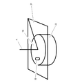
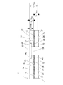
本明細書及び特許請求の範囲の中で研磨面(14)を有する化学機械研磨パッド(10)に関して使用される「平均全厚さTT-avg」とは、研磨面(14)に対して垂直な方向に研磨面(14)から硬質層(25)の下面(27)までで計測される化学機械研磨パッドの平均厚さTTをいう(図1、2、5及び7〜10を参照)。 The “average total thickness T T-avg ” used with respect to a chemical mechanical polishing pad (10) having a polishing surface (14) within the specification and claims is relative to the polishing surface (14). Refers to the average thickness T T of the chemical mechanical polishing pad measured in the vertical direction from the polishing surface (14) to the lower surface (27) of the hard layer (25) (see FIGS. 1, 2, 5 and 7-10). ).
本明細書及び特許請求の範囲の中で研磨層に関して使用される「初期加水分解安定性」とは、実施例に記載される手順にしたがって計測して、研磨層の試料の長さ寸法が25℃の脱イオン水中24時間の浸漬ののち<1%変化することをいう。 As used herein and in the claims, “initial hydrolysis stability” as used with respect to the polishing layer is measured according to the procedure described in the examples and the length dimension of the sample of the polishing layer is 25. A change of <1% after 24 hours of immersion in deionized water at 0 ° C.
本明細書及び特許請求の範囲の中で研磨層に関して使用される「長期加水分解安定性」とは、実施例に記載される手順にしたがって計測して、研磨層の試料の長さ寸法が25℃の脱イオン水中7日間の浸漬ののち<1.75%変化することをいう。 “Long-term hydrolysis stability” as used in the specification and claims with respect to the polishing layer is measured according to the procedure described in the examples, and the length dimension of the sample of the polishing layer is 25. A change of <1.75% after 7 days of immersion in deionized water at 0 ° C.
本明細書及び特許請求の範囲の中で研磨層に関して使用される「持続的加水分解不安定性」とは、実施例に記載される手順にしたがって計測して、研磨層の試料の長さ寸法が25℃の脱イオン水中7日間の浸漬ののち≧1.75%変化することをいう。 As used herein and in the claims, “persistent hydrolysis instability” refers to the length dimension of the sample of the polishing layer as measured according to the procedure described in the examples. A change of ≧ 1.75% after 7 days of immersion in deionized water at 25 ° C.
本明細書及び特許請求の範囲の中で化学機械研磨パッド(10)に関して使用される「実質的に円形の断面」とは、中心軸(12)から研磨層(20)の研磨面(14)の外周(15)までの断面の最長半径rが中心軸(12)から研磨面(14)の外周(15)までの断面の最短半径rよりも≦20%しか長くないことをいう(図1を参照)。 “Substantially circular cross-section” as used in connection with the chemical mechanical polishing pad (10) in this specification and claims refers to the polishing surface (14) of the polishing layer (20) from the central axis (12). The longest radius r of the cross section up to the outer periphery (15) of the steel is only ≦ 20% longer than the shortest radius r of the cross section from the central axis (12) to the outer periphery (15) of the polishing surface (14) (FIG. 1). See).
本発明の基材を化学機械研磨する方法は、磁性基材、光学基材及び半導体基材の少なくとも一つから選択される基材を提供する工程、(A)組成及び研磨面を有する研磨層であって、組成が、(i)研磨層の試料の長さ寸法が25℃の脱イオン水中24時間の浸漬ののち<1%変化する初期加水分解安定性を(ii)研磨層の試料の長さ寸法が25℃の脱イオン水中7日間の浸漬ののち≧1.75%変化する持続的加水分解不安定性と併せて示すように選択されている研磨層と、(B)上面及び下面を有する硬質層と、(C)研磨層のベース面と硬質層の上面との間に挿入された、研磨層を硬質層に接着するホットメルト接着剤と、(D)スタック側及びプラテン側を有する感圧プラテン接着剤層であって、スタック側が硬質層の下面に隣接する感圧プラテン接着剤層と、(E)場合によっては、感圧プラテン接着剤層のプラテン側に配置される任意選択の剥離ライナと、(F)場合によっては、終点検出ウィンドウと、(G)場合によっては、硬質層の下面及び感圧プラテン接着剤層のスタック側と対面し、それらの間に挿入される少なくとも一つのさらなる層とを含む化学機械研磨パッドを提供する工程、及び研磨面と基材との間に動的接触を生じさせて基材の表面を研磨する工程を含む。 The method of chemically mechanically polishing a substrate of the present invention includes a step of providing a substrate selected from at least one of a magnetic substrate, an optical substrate and a semiconductor substrate, (A) a polishing layer having a composition and a polished surface Wherein the composition has (i) an initial hydrolysis stability that changes <1% after immersion for 24 hours in deionized water at 25 ° C. in the length dimension of the sample of the polishing layer (ii) of the sample of the polishing layer A polishing layer selected to show in combination with a persistent hydrolysis instability that changes ≧ 1.75% after 7 days of immersion in deionized water at 25 ° C. in length, and (B) the top and bottom surfaces A hard layer having (C) a hot melt adhesive that is inserted between the base surface of the polishing layer and the upper surface of the hard layer, and (D) a stack side and a platen side. A pressure sensitive platen adhesive layer with the stack side adjacent to the underside of the hard layer A pressure-sensitive platen adhesive layer; (E) an optional release liner disposed on the platen side of the pressure-sensitive platen adhesive layer; (F) an endpoint detection window; Optionally providing a chemical mechanical polishing pad comprising a lower surface of the hard layer and a stack side of the pressure sensitive platen adhesive layer, and comprising at least one additional layer interposed therebetween, and a polishing surface; A step of polishing the surface of the substrate by generating dynamic contact with the substrate;
好ましくは、本発明の方法において提供される基材は半導体基材である。より好ましくは、提供される基材は、露出した銅フィーチャーを有する表面を有する半導体基材である。 Preferably, the substrate provided in the method of the present invention is a semiconductor substrate. More preferably, the provided substrate is a semiconductor substrate having a surface with exposed copper features.
好ましくは、本発明の方法において提供される化学機械研磨パッド(10)は、研磨面(14)、ベース面(17)及び研磨面(14)に対して垂直な方向に研磨面(14)からベース面(17)までで計測される平均厚さTP-avgを有する研磨層(20)と、上面(26)及び下面(27)を有する硬質層(25)と、研磨層(20)のベース面(17)と硬質層(25)の上面(26)との間に挿入された、研磨層(20)を硬質層(25)に接着するホットメルト接着剤(23)と、場合によっては、スタック側(72)及びプラテン側(74)を有し、硬質層(25)の下面(27)に配置される感圧プラテン接着剤層(70)(好ましくは、任意選択の感圧プラテン接着剤層は、研磨機への化学機械研磨パッドの取り付けを容易にする)と、場合によっては、剥離ライナ(75)(感圧プラテン接着剤層(70)が硬質層(25)の下面(27)と任意選択の剥離ライナ(75)との間に挿入される)と、場合によっては、終点検出ウィンドウ(30)(好ましくは、終点検出ウィンドウはインサイチュー研磨終点検出を容易にする)と、場合によっては、硬質層(25)の下面(27)及び感圧プラテン接着剤層(70)のスタック側(72)と対面し、それらの間に挿入される少なくとも一つのさらなる層(図示せず)とを含む(図1〜10を参照)。 Preferably, the chemical mechanical polishing pad (10) provided in the method of the invention is from the polishing surface (14) in a direction perpendicular to the polishing surface (14), the base surface (17) and the polishing surface (14). A polishing layer (20) having an average thickness T P-avg measured up to the base surface (17), a hard layer (25) having an upper surface (26) and a lower surface (27), and a polishing layer (20). A hot melt adhesive (23) inserted between the base surface (17) and the upper surface (26) of the hard layer (25) to bond the abrasive layer (20) to the hard layer (25), and possibly A pressure-sensitive platen adhesive layer (70) having a stack side (72) and a platen side (74) and disposed on the lower surface (27) of the hard layer (25) (preferably an optional pressure-sensitive platen bond) The agent layer facilitates the attachment of chemical mechanical polishing pads to the polishing machine. ) And, in some cases, a release liner (75) (a pressure sensitive platen adhesive layer (70) is inserted between the lower surface (27) of the hard layer (25) and the optional release liner (75)). And, optionally, an endpoint detection window (30) (preferably the endpoint detection window facilitates in situ polishing endpoint detection), and in some cases, the lower surface (27) of the hard layer (25) and the pressure sensitive platen. It includes at least one additional layer (not shown) facing the stack side (72) of the adhesive layer (70) and inserted therebetween (see FIGS. 1-10).
好ましくは、本発明の方法において提供される化学機械研磨パッド(10)は、中心軸(12)を中心に回転するように適合されている(図1を参照)。好ましくは、研磨層(20)の研磨面(14)は、中心軸(12)に対して垂直な平面(28)にある。本発明の方法において提供される化学機械研磨パッド(10)は、好ましくは、中心軸(12)に対して85〜95°、好ましくは中心軸(12)に対して90°の角度γにある平面(28)において回転するように適合されている。好ましくは、研磨層(20)は、中心軸(12)に対して垂直な実質的に円形の断面を有する研磨面(14)を有する。好ましくは、中心軸(12)に対して垂直な研磨面(14)の断面の半径rは、断面に関して≦20%、より好ましくは断面に関して≦10%しか変化しない。 Preferably, the chemical mechanical polishing pad (10) provided in the method of the present invention is adapted to rotate about a central axis (12) (see FIG. 1). Preferably, the polishing surface (14) of the polishing layer (20) is in a plane (28) perpendicular to the central axis (12). The chemical mechanical polishing pad (10) provided in the method of the present invention is preferably at an angle γ of 85 to 95 ° with respect to the central axis (12), preferably 90 ° with respect to the central axis (12). Adapted to rotate in the plane (28). Preferably, the polishing layer (20) has a polishing surface (14) having a substantially circular cross section perpendicular to the central axis (12). Preferably, the radius r of the cross section of the polishing surface (14) perpendicular to the central axis (12) varies only ≦ 20% with respect to the cross section, more preferably ≦ 10% with respect to the cross section.
好ましくは、本発明の方法において提供される化学機械研磨パッドは、磁性基材、光学基材及び半導体基材の少なくとも一つから選択される基材の研磨を容易にするように具体的に設計されている。好ましくは、本発明の化学機械研磨パッドは、半導体基材の研磨を容易にするように設計されている。より好ましくは、本発明の化学機械研磨パッドは、半導体ウェーハ基材の表面上の露出した銅フィーチャーの研磨を容易にするように設計されている。 Preferably, the chemical mechanical polishing pad provided in the method of the present invention is specifically designed to facilitate polishing of a substrate selected from at least one of a magnetic substrate, an optical substrate and a semiconductor substrate. Has been. Preferably, the chemical mechanical polishing pad of the present invention is designed to facilitate polishing of a semiconductor substrate. More preferably, the chemical mechanical polishing pad of the present invention is designed to facilitate polishing of exposed copper features on the surface of a semiconductor wafer substrate.
本発明の方法において提供される化学機械研磨パッドは、組成を有する研磨層であって、組成が、(i)研磨層の試料の長さ寸法が25℃の脱イオン水中24時間の浸漬ののち<1%変化する初期加水分解安定性を(ii)研磨層の試料の長さ寸法が25℃の脱イオン水中7日間の浸漬ののち≧1.75%変化する持続的加水分解不安定性と併せて示すように選択されている研磨層を含む。 The chemical mechanical polishing pad provided in the method of the present invention is a polishing layer having a composition, wherein the composition is (i) after immersion for 24 hours in deionized water having a sample length of the polishing layer of 25 ° C. <1% change in initial hydrolysis stability with (ii) continuous hydrolysis instability that changes ≧ 1.75% after 7 days of immersion in deionized water at 25 ° C. in the length dimension of the polishing layer sample A polishing layer selected as shown.
好ましくは、本発明の方法において提供される化学機械研磨パッドに使用される研磨層の組成は、ポリ(ウレタン)、ポリスルホン、ポリエーテルスルホン、ナイロン、ポリエーテル、ポリエステル、ポリスチレン、アクリルポリマー、ポリウレア、ポリアミド、ポリ塩化ビニル、ポリフッ化ビニル、ポリエチレン、ポリプロピレン、ポリブタジエン、ポリエチレンイミン、ポリアクリロニトリル、ポリエチレンオキシド、ポリオレフィン、ポリ(アルキル)アクリレート、ポリ(アルキル)メタクリレート、ポリアミド、ポリエーテルイミド、ポリケトン、エポキシ、シリコーン、エチレンプロピレンジエンモノマーから形成されるポリマー、タンパク質、多糖類、ポリアセテート及び前記の少なくとも二つの組み合わせからなる群より選択される。好ましくは、本発明の方法において提供される化学機械研磨パッドに使用される研磨層の組成はポリ(ウレタン)を含む。より好ましくは、本発明の方法において提供される化学機械研磨パッドに使用される研磨層の組成はポリウレタンである。 Preferably, the composition of the polishing layer used in the chemical mechanical polishing pad provided in the method of the present invention is poly (urethane), polysulfone, polyethersulfone, nylon, polyether, polyester, polystyrene, acrylic polymer, polyurea, Polyamide, polyvinyl chloride, polyvinyl fluoride, polyethylene, polypropylene, polybutadiene, polyethyleneimine, polyacrylonitrile, polyethylene oxide, polyolefin, poly (alkyl) acrylate, poly (alkyl) methacrylate, polyamide, polyetherimide, polyketone, epoxy, silicone Selected from the group consisting of polymers formed from ethylene propylene diene monomers, proteins, polysaccharides, polyacetates and combinations of at least two of the foregoing. It is. Preferably, the composition of the polishing layer used in the chemical mechanical polishing pad provided in the method of the present invention comprises poly (urethane). More preferably, the composition of the polishing layer used in the chemical mechanical polishing pad provided in the method of the present invention is polyurethane.
好ましくは、本発明の方法において提供される化学機械研磨パッドに使用される研磨層の組成は、ポリイソシアネート(たとえばジイソシアネート)と、ヒドロキシル含有材料と、場合によっては硬化剤との反応生成物である。 Preferably, the composition of the polishing layer used in the chemical mechanical polishing pad provided in the method of the present invention is the reaction product of a polyisocyanate (eg, diisocyanate), a hydroxyl-containing material, and optionally a curing agent. .
好ましくは、ポリイソシアネートは、メチレンビス4,4′−シクロヘキシル−イソシアネート、シクロヘキシルジイソシアネート、イソホロンジイソシアネート、ヘキサメチレンジイソシアネート、プロピレン−1,2−ジイソシアネート、テトラメチレン−1,4−ジイソシアネート、1,6−ヘキサメチレン−ジイソシアネート、ドデカン−1,12−ジイソシアネート、シクロブタン−1,3−ジイソシアネート、シクロヘキサン−1,3−ジイソシアネート、シクロヘキサン−1,4−ジイソシアネート、1−イソシアナト−3,3,5−トリメチル−5−イソシアナトメチルシクロヘキサン、メチルシクロヘキシレンジイソシアネート、ヘキサメチレンジイソシアネートのトリイソシアネート、2,4,4−トリメチル−1,6−ヘキサンジイソシアネートのトリイソシアネート、ヘキサメチレンジイソシアネートのウレトジオン、エチレンジイソシアネート、2,2,4−トリメチルヘキサメチレンジイソシアネート、2,4,4−トリメチルヘキサメチレンジイソシアネート、ジシクロヘキシルメタンジイソシアネート及びそれらの組み合わせを含む。より好ましくは、ポリイソシアネートは脂肪族であり、14%未満の未反応のイソシアネート基を有する。 Preferably, the polyisocyanate is methylene bis 4,4'-cyclohexyl-isocyanate, cyclohexyl diisocyanate, isophorone diisocyanate, hexamethylene diisocyanate, propylene-1,2-diisocyanate, tetramethylene-1,4-diisocyanate, 1,6-hexamethylene. Diisocyanate, dodecane-1,12-diisocyanate, cyclobutane-1,3-diisocyanate, cyclohexane-1,3-diisocyanate, cyclohexane-1,4-diisocyanate, 1-isocyanato-3,3,5-trimethyl-5-isocyanate Natomethylcyclohexane, methylcyclohexylene diisocyanate, triisocyanate of hexamethylene diisocyanate, 2,4,4-trimethyl-1,6 Triisocyanate hexane diisocyanate, including uretdione of hexamethylene diisocyanate, ethylene diisocyanate, 2,2,4-trimethylhexamethylene diisocyanate, 2,4,4-trimethylhexamethylene diisocyanate, dicyclohexylmethane diisocyanate, and combinations thereof. More preferably, the polyisocyanate is aliphatic and has less than 14% unreacted isocyanate groups.
好ましくは、ヒドロキシル含有材料はポリオールを含む。例示的なポリオールは、たとえば、ポリエーテルポリオール、ヒドロキシ末端ポリブタジエン(部分的及び完全に水素化された誘導体を含む)、ポリエステルポリオール、ポリカプロラクトンポリオール、ポリカーボネートポリオール及びそれらの混合物を含む。 Preferably, the hydroxyl-containing material includes a polyol. Exemplary polyols include, for example, polyether polyols, hydroxy-terminated polybutadienes (including partially and fully hydrogenated derivatives), polyester polyols, polycaprolactone polyols, polycarbonate polyols and mixtures thereof.
好ましいポリオールはポリエーテルポリオールを含む。ポリエーテルポリオールの例は、ポリテトラメチレンエーテルグリコール(「PTMEG」)、ポリエチレンプロピレングリコール、ポリオキシプロピレングリコール及びそれらの混合物を含む。炭化水素鎖は、飽和又は不飽和結合を有することもできるし、置換又は非置換の芳香族及び環式基を有することもできる。好ましくは、本発明のポリオールはPTMEGを含む。好ましいポリエステルポリオールは、ポリエチレンアジペートグリコール、ポリブチレンアジペートグリコール、ポリエチレンプロピレンアジペートグリコール、o−フタレート−1,6−ヘキサンジオール、ポリ(ヘキサメチレンアジペート)グリコール及びそれらの混合物を含むが、それらに限定されない。炭化水素鎖は、飽和又は不飽和結合を有することもできるし、置換又は非置換の芳香族及び環式基を有することもできる。好ましいポリカプロラクトンポリオールは、1,6−ヘキサンジオール誘導ポリカプロラクトン、ジエチレングリコール誘導ポリカプロラクトン、トリメチロールプロパン誘導ポリカプロラクトン、ネオペンチルグリコール誘導ポリカプロラクトン、1,4−ブタンジオール誘導ポリカプロラクトン、PTMEG誘導ポリカプロラクトン及びそれらの混合物を含むが、それらに限定されない。炭化水素鎖は、飽和又は不飽和結合を有することもできるし、置換又は非置換の芳香族及び環式基を有することもできる。好ましいポリカーボネートは、ポリフタレートカーボネート及びポリ(ヘキサメチレンカーボネート)グリコールを含むが、それらに限定されない。 Preferred polyols include polyether polyols. Examples of polyether polyols include polytetramethylene ether glycol (“PTMEG”), polyethylene propylene glycol, polyoxypropylene glycol, and mixtures thereof. The hydrocarbon chain can have saturated or unsaturated bonds and can have substituted or unsubstituted aromatic and cyclic groups. Preferably, the polyol of the present invention comprises PTMEG. Preferred polyester polyols include, but are not limited to, polyethylene adipate glycol, polybutylene adipate glycol, polyethylene propylene adipate glycol, o-phthalate-1,6-hexanediol, poly (hexamethylene adipate) glycol, and mixtures thereof. The hydrocarbon chain can have saturated or unsaturated bonds and can have substituted or unsubstituted aromatic and cyclic groups. Preferred polycaprolactone polyols are 1,6-hexanediol derived polycaprolactone, diethylene glycol derived polycaprolactone, trimethylolpropane derived polycaprolactone, neopentyl glycol derived polycaprolactone, 1,4-butanediol derived polycaprolactone, PTMEG derived polycaprolactone and Including but not limited to mixtures thereof. The hydrocarbon chain can have saturated or unsaturated bonds and can have substituted or unsubstituted aromatic and cyclic groups. Preferred polycarbonates include but are not limited to polyphthalate carbonate and poly (hexamethylene carbonate) glycol.
好ましい硬化剤はジアミンを含む。好ましいポリジアミンは第一級アミン及び第二級アミンを含む。より好ましいポリジアミンは、ジエチルトルエンジアミン(「DETDA」)、3,5−ジメチルチオ−2,4−トルエンジアミン及びその異性体、3,5−ジエチルトルエン−2,4−ジアミン及びその異性体(たとえば3,5−ジエチルトルエン−2,6−ジアミン)、4,4′−ビス−(sec−ブチルアミノ)−ジフェニルメタン、1,4−ビス−(sec−ブチルアミノ)−ベンゼン、4,4′−メチレン−ビス−(2−クロロアニリン)、4,4′−メチレン−ビス−(3−クロロ−2,6−ジエチルアニリン)(「MCDEA」)、ポリテトラメチレンオキシド−ジ−p−アミノベンゾエート、N,N′−ジアルキルジアミノジフェニルメタン、p,p′−メチレンジアニリン(「MDA」)、m−フェニレンジアミン(「MPDA」)、メチレン−ビス2−クロロアニリン(「MBOCA」)、4,4′−メチレン−ビス−(2−クロロアニリン)(「MOCA」)、4,4′−メチレン−ビス−(2,6−ジエチルアニリン)(「MDEA」)、4,4′−メチレン−ビス−(2,3−ジクロロアニリン)(「MDCA」)、4,4′−ジアミノ−3,3′−ジエチル−5,5′−ジメチルジフェニルメタン、2,2′,3,3′−テトラクロロジアミノジフェニルメタン、トリメチレングリコールジ−p−アミノベンゾエート及びそれらの混合物を含む。 Preferred curing agents include diamines. Preferred polydiamines include primary amines and secondary amines. More preferred polydiamines are diethyltoluenediamine (“DETDA”), 3,5-dimethylthio-2,4-toluenediamine and its isomers, 3,5-diethyltoluene-2,4-diamine and its isomers (eg 3 , 5-diethyltoluene-2,6-diamine), 4,4'-bis- (sec-butylamino) -diphenylmethane, 1,4-bis- (sec-butylamino) -benzene, 4,4'-methylene -Bis- (2-chloroaniline), 4,4'-methylene-bis- (3-chloro-2,6-diethylaniline) ("MCDEA"), polytetramethylene oxide-di-p-aminobenzoate, N , N'-dialkyldiaminodiphenylmethane, p, p'-methylenedianiline ("MDA"), m-phenylenediamine ("MPDA") , Methylene-bis 2-chloroaniline (“MBOCA”), 4,4′-methylene-bis- (2-chloroaniline) (“MOCA”), 4,4′-methylene-bis- (2,6-diethyl) Aniline) ("MDEA"), 4,4'-methylene-bis- (2,3-dichloroaniline) ("MDCA"), 4,4'-diamino-3,3'-diethyl-5,5'- Dimethyldiphenylmethane, 2,2 ', 3,3'-tetrachlorodiaminodiphenylmethane, trimethylene glycol di-p-aminobenzoate and mixtures thereof.
硬化剤はまた、ジオール、トリオール、テトラオール及びヒドロキシ末端硬化剤を含むことができる。好ましいジオール、トリオール及びテトラオールは、エチレングリコール、ジエチレングリコール、ポリエチレングリコール、プロピレングリコール、ポリプロピレングリコール、低分子量ポリテトラメチレンエーテルグリコール、1,3−ビス(2−ヒドロキシエトキシ)ベンゼン、1,3−ビス−[2−(2−ヒドロキシエトキシ)エトキシ]ベンゼン、1,3−ビス−{2−[2−(2−ヒドロキシエトキシ)エトキシ]エトキシ}ベンゼン、1,4−ブタンジオール、1,5−ペンタンジオール、1,6−ヘキサンジオール、レソルシノール−ジ−(β−ヒドロキシエチル)エーテル、ヒドロキノン−ジ−(β−ヒドロキシエチル)エーテル及びそれらの混合物を含む。好ましいヒドロキシ末端硬化剤は、1,3−ビス(2−ヒドロキシエトキシ)ベンゼン、1,3−ビス−[2−(2−ヒドロキシエトキシ)エトキシ]ベンゼン、1,3−ビス−{2−[2−(2−ヒドロキシエトキシ)エトキシ]エトキシ}ベンゼン、1,4−ブタンジオール及びそれらの混合物を含む。ヒドロキシ末端硬化剤及びジアミン硬化剤は、一つ以上の飽和、不飽和、芳香族及び環式基を含むことができる。加えて、ヒドロキシ末端硬化剤及びジアミン硬化剤は一つ以上のハロゲン基を含むことができる。
Curing agents can also include diols, triols, tetraols and hydroxy-terminated curing agents. Preferred diols, triols and tetraols are ethylene glycol, diethylene glycol, polyethylene glycol, propylene glycol, polypropylene glycol, low molecular weight polytetramethylene ether glycol, 1,3-bis (2-hydroxyethoxy) benzene, 1,3-bis- [2- (2-hydroxyethoxy) ethoxy] benzene, 1,3-bis- {2- [2- (2-hydroxyethoxy) ethoxy] ethoxy} benzene, 1,4-butanediol, 1,5-
好ましくは、本発明の方法において提供される化学機械研磨パッドに使用される研磨層は複数の微小エレメントを含む。好ましくは、複数の微小エレメントは、本発明の方法において提供される化学機械研磨パッドに使用される研磨層全体に均一に分散している。好ましくは、複数の微小エレメントは、閉じ込められた気泡、中空コアポリマー材料、液体充填中空コアポリマー材料、水溶性材料、不溶相材料(たとえば鉱油)及びそれらの組み合わせから選択される。より好ましくは、複数の微小エレメントは、本発明の方法において提供される化学機械研磨パッドに使用される研磨層全体に均一に分散している閉じ込められた気泡及び中空コアポリマー材料から選択される。好ましくは、複数の微小エレメントは、150μm未満(より好ましくは50μm未満、もっとも好ましくは10〜50μm)の重量平均直径を有する。好ましくは、複数の微小エレメントは、ポリアクリロニトリル又はポリアクリロニトリルコポリマーのシェル壁を有するポリマーマイクロバルーン(たとえばAkzo NobelのExpancel(登録商標))を含む。好ましくは、複数の微小エレメントは、0〜35容量%の気孔率(より好ましくは10〜25容量%の気孔率)で、本発明の方法において提供される化学機械研磨パッドに使用される研磨層に組み込まれる。 Preferably, the polishing layer used in the chemical mechanical polishing pad provided in the method of the present invention comprises a plurality of microelements. Preferably, the plurality of microelements are uniformly distributed throughout the polishing layer used in the chemical mechanical polishing pad provided in the method of the present invention. Preferably, the plurality of microelements are selected from confined bubbles, hollow core polymer material, liquid filled hollow core polymer material, water soluble material, insoluble phase material (eg mineral oil) and combinations thereof. More preferably, the plurality of microelements are selected from confined cellular and hollow core polymeric materials that are uniformly distributed throughout the polishing layer used in the chemical mechanical polishing pad provided in the method of the present invention. Preferably, the plurality of microelements have a weight average diameter of less than 150 μm (more preferably less than 50 μm, most preferably 10 to 50 μm). Preferably, the plurality of microelements comprises a polymer microballoon (eg Akzo Nobel's Expancel®) with a shell wall of polyacrylonitrile or polyacrylonitrile copolymer. Preferably, the plurality of microelements have a porosity of 0 to 35% by volume (more preferably 10 to 25% by volume), and a polishing layer used in a chemical mechanical polishing pad provided in the method of the present invention. Incorporated into.
本発明の方法において提供される化学機械研磨パッドに使用される研磨層は、多孔構造及び無孔(すなわち非充填)構造の両方で提供することができる。好ましくは、本発明の方法において提供される化学機械研磨パッドに使用される研磨層は、ASTM D1622にしたがって計測して0.6よりも高い比重を示す。より好ましくは、本発明の方法において提供される化学機械研磨パッドに使用される研磨層は、ASTM D1622にしたがって計測して0.6〜1.5(さらに好ましくは0.7〜1.2、もっとも好ましくは0.95〜1.2)の比重を示す。 The polishing layer used in the chemical mechanical polishing pad provided in the method of the present invention can be provided in both a porous structure and a non-porous (ie, unfilled) structure. Preferably, the polishing layer used in the chemical mechanical polishing pad provided in the method of the present invention exhibits a specific gravity greater than 0.6 as measured according to ASTM D1622. More preferably, the polishing layer used in the chemical mechanical polishing pad provided in the method of the present invention is 0.6-1.5 (more preferably 0.7-1.2, more preferably) measured according to ASTM D1622. Most preferably, it has a specific gravity of 0.95 to 1.2).
好ましくは、本発明の方法において提供される化学機械研磨パッドに使用される研磨層は、ASTM D2240にしたがって計測して60〜90のショアD硬さを示す。より好ましくは、本発明の方法において提供される化学機械研磨パッドに使用される研磨層は、ASTM D2240にしたがって計測して>60〜75(より好ましくは61〜75、もっとも好ましくは>65〜70)のショアD硬さを示す。 Preferably, the polishing layer used in the chemical mechanical polishing pad provided in the method of the present invention exhibits a Shore D hardness of 60-90 as measured according to ASTM D2240. More preferably, the polishing layer used in the chemical mechanical polishing pad provided in the method of the present invention is> 60 to 75 (more preferably 61 to 75, most preferably> 65 to 70) as measured according to ASTM D2240. ) Shore D hardness.
好ましくは、本発明の方法において提供される化学機械研磨パッドに使用される研磨層は、ASTM D412にしたがって計測して100〜300%の破断点伸びを示す。好ましくは、本発明の方法において提供される化学機械研磨パッドに使用される研磨層は、ASTM D412にしたがって計測して100〜200%(さらに好ましくは125〜175%、もっとも好ましくは150〜160%)の破断点伸びを示す。 Preferably, the polishing layer used in the chemical mechanical polishing pad provided in the method of the present invention exhibits an elongation at break of 100-300% as measured according to ASTM D412. Preferably, the polishing layer used in the chemical mechanical polishing pad provided in the method of the present invention is 100-200% (more preferably 125-175%, most preferably 150-160%) measured according to ASTM D412. ) Shows the elongation at break.
当業者は、所与の研磨作業のために本発明の方法において提供される化学機械研磨パッド(10)における使用に適した厚さTPを有する研磨層(20)を選択する方法を理解するであろう。好ましくは、本発明の方法において提供される化学機械研磨パッド(10)に使用される研磨層(20)は、研磨面(14)の平面(28)に対して垂直な軸(A)に沿って平均厚さTP-avgを示す。より好ましくは、平均厚さTP-avgは20〜150ミル(より好ましくは30〜130ミル、もっとも好ましくは70〜90ミル)である(図2、5及び7〜10を参照)。 Those skilled in the art will understand how to select a polishing layer (20) having a thickness T P suitable for use in the chemical mechanical polishing pad which is provided in the method of the present invention (10) for a given polishing operation Will. Preferably, the polishing layer (20) used in the chemical mechanical polishing pad (10) provided in the method of the present invention is along an axis (A) perpendicular to the plane (28) of the polishing surface (14). Mean thickness TP-avg . More preferably, the average thickness T P-avg is 20-150 mils (more preferably 30-130 mils, most preferably 70-90 mils) (see FIGS. 2, 5 and 7-10).
好ましくは、本発明の方法において提供される化学機械研磨パッドに使用される研磨層の研磨面は、磁性基材、光学基材及び半導体基材の少なくとも一つから選択される基材(より好ましくは半導体基材、さらに好ましくは半導体ウェーハ、もっとも好ましくは、露出した銅フィーチャーを有する面を有する半導体ウェーハ)を研磨するように適合されている。本発明の方法において提供される化学機械研磨パッドに使用される研磨層の研磨面は、基材の研磨を促進するためにマクロテキスチャ及びミクロテキスチャの少なくとも一つを示す。好ましくは、研磨面はマクロテキスチャを示し、マクロテキスチャは、(i)ハイドロプレーニングの少なくとも1つを緩和すること、(ii)研磨媒の流れに影響すること、(iii)研磨層の剛性を変化させること、(iv)エッジ効果を減らすこと、及び(v)研磨面と研磨される基材との間の区域からの研磨くずの運び出しを促進することの少なくとも一つを実行するように設計されている。 Preferably, the polishing surface of the polishing layer used in the chemical mechanical polishing pad provided in the method of the present invention is a substrate selected from at least one of a magnetic substrate, an optical substrate and a semiconductor substrate (more preferably Is adapted to polish a semiconductor substrate, more preferably a semiconductor wafer, most preferably a semiconductor wafer having a surface with exposed copper features. The polishing surface of the polishing layer used in the chemical mechanical polishing pad provided in the method of the present invention exhibits at least one of macrotexture and microtexture to promote polishing of the substrate. Preferably, the polishing surface exhibits macrotexture, the macrotexture being (i) relaxing at least one of the hydroplaning, (ii) affecting the flow of the polishing medium, (iii) changing the stiffness of the polishing layer. Designed to perform at least one of: (iv) reducing edge effects; and (v) facilitating removal of abrasive debris from the area between the polishing surface and the substrate being polished. ing.
研磨面は、好ましくは、穿孔及び溝の少なくとも一つから選択されるマクロテキスチャを示す。好ましくは、穿孔は、研磨面から発明の方法において提供される化学機械研磨パッドに使用される研磨層の厚さの途中まで又は全部に延びることができる。好ましくは、溝は、研磨中にパッドが回転すると、少なくとも一つの溝が基材の上を掃くように研磨面上に配設される。好ましくは、溝は、カーブした溝、直線状の溝及びそれらの組み合わせから選択される。溝は、≧10ミル(好ましくは10〜120ミル)の深さを示す。好ましくは、溝は、≧10ミル、≧15ミル及び15〜120ミルから選択される深さ、≧10ミル及び10〜100ミルから選択される幅ならびに≧30ミル、≧50ミル、50〜200ミル、70〜200ミル及び90〜200ミルから選択されるピッチの組み合わせを有する少なくとも二つの溝を含む溝パターンを形成する。 The polished surface preferably exhibits a macrotexture selected from at least one of perforations and grooves. Preferably, the perforations can extend from the polishing surface halfway through or through the thickness of the polishing layer used in the chemical mechanical polishing pad provided in the method of the invention. Preferably, the grooves are disposed on the polishing surface such that at least one groove sweeps over the substrate as the pad rotates during polishing. Preferably, the grooves are selected from curved grooves, straight grooves and combinations thereof. The grooves exhibit a depth of ≧ 10 mils (preferably 10-120 mils). Preferably, the groove has a depth selected from ≧ 10 mils, ≧ 15 mils and 15-120 mils, a width selected from ≧ 10 mils and 10-100 mils and ≧ 30 mils, ≧ 50 mils, 50-200. A groove pattern is formed that includes at least two grooves having a combination of pitches selected from a mill, 70-200 mil and 90-200 mil.
好ましくは、本発明の方法において提供される化学機械研磨パッドに使用される研磨層は、その中に組み込まれた砥粒<1ppmを含有する。 Preferably, the polishing layer used in the chemical mechanical polishing pad provided in the method of the present invention contains abrasive grains <1 ppm incorporated therein.
本発明の方法において提供される化学機械研磨パッドに使用される好ましい研磨層組成はポリウレタンであり、ポリウレタンは、(a)(i)トルエンジイソシアネート(好ましくは、2,4−トルエンジイソシアネート、2,6−トルエンジイソシアネート及びそれらの混合物から選択されるトルエンジイソシアネート)と(ii)ポリプロピレングルコール系ポリオールとの反応によって得られる、8〜9.5重量%(好ましくは8.65〜9.05重量%、より好ましくは>8.7〜9重量%)の未反応NCOを有するポリプロピレングルコール系イソシアネート末端ウレタンプレポリマー、(b)4,4′−メチレン−ビス−(2−クロロアニリン)である硬化剤、及び(c)場合によっては、複数の微小エレメントを含む成分の反応生成物であり、研磨層は、0.6よりも高い比重、60〜90(好ましくは>60〜75、より好ましくは61〜75、もっとも好ましくは>65〜70)のショアD硬さ及び100〜300%(好ましくは100〜200%、より好ましくは125〜175%、もっとも好ましくは150〜160%)の破断点伸びを示し、研磨層は、研磨層の試料の長さ寸法が25℃の脱イオン水中24時間の浸漬ののち<1%変化する初期加水分解安定性(実施例に記載される方法にしたがって計測)を示し、研磨層は、研磨層の試料の長さ寸法が25℃の脱イオン水中7日間の浸漬ののち≧1.75%(好ましくは1.75〜5%、より好ましくは1.75〜3.5%、もっとも好ましくは2〜3%)変化する持続的加水分解不安定性(実施例に記載される方法にしたがって計測)を示す。好ましくは、本発明の方法において提供される化学機械研磨パッドに使用される研磨層の形成に使用されるポリプロピレングルコール系イソシアネート末端ウレタンプレポリマー中の未反応イソシアネート(NCO)基に対する硬化剤中の反応性水素基(すなわちアミン(NH2)基とヒドロキシル(OH)基との合計)の化学量論比は80〜<95%(より好ましくは85〜<95%、さらに好ましくは87〜94%、もっとも好ましくは89〜92%)である。好ましくは、発明の方法において提供される化学機械研磨パッドに使用される研磨層の形成に使用されるポリプロピレングルコール系イソシアネート末端ウレタンプレポリマーは、0.1重量%未満の遊離トルエンジイソシアネート(TDI)モノマー含量を有する、低遊離のイソシアネート末端ウレタンプレポリマーである。 The preferred polishing layer composition used in the chemical mechanical polishing pad provided in the method of the present invention is polyurethane, and the polyurethane is (a) (i) toluene diisocyanate (preferably 2,4-toluene diisocyanate, 2,6 -Toluene diisocyanate selected from toluene diisocyanate and mixtures thereof) and (ii) 8 to 9.5% by weight (preferably 8.65 to 9.05% by weight) obtained by reaction of polypropylene glycol-based polyol, More preferably> 8.7-9 wt%) polypropylene glycol based isocyanate terminated urethane prepolymer with unreacted NCO, (b) a curing agent which is 4,4'-methylene-bis- (2-chloroaniline) And (c) reaction of a component comprising a plurality of microelements in some cases The composition, the polishing layer, has a specific gravity greater than 0.6, a Shore D hardness of 100-90 (preferably> 60-75, more preferably 61-75, most preferably> 65-70) and 100 Exhibit an elongation at break of ˜300% (preferably 100-200%, more preferably 125-175%, most preferably 150-160%) and the polishing layer has a sample length dimension of 25 ° C. Shows initial hydrolysis stability (measured according to the method described in the Examples), which changes <1% after immersion in deionized water for 24 hours, and the polishing layer has a sample length dimension of 25 ° C. Sustained hydrolysis that changes ≧ 1.75% (preferably 1.75-5%, more preferably 1.75-3.5%, most preferably 2-3%) after 7 days immersion in deionized water Instability (as described in the examples) According to the method to be measured). Preferably, in a curing agent for unreacted isocyanate (NCO) groups in a polypropylene glycol-based isocyanate-terminated urethane prepolymer used to form a polishing layer used in the chemical mechanical polishing pad provided in the method of the present invention. The stoichiometric ratio of reactive hydrogen groups (ie, the sum of amine (NH 2 ) groups and hydroxyl (OH) groups) is 80 to <95% (more preferably 85 to <95%, more preferably 87 to 94%). , Most preferably 89-92%). Preferably, the polypropylene glycol-based isocyanate-terminated urethane prepolymer used to form the polishing layer used in the chemical mechanical polishing pad provided in the method of the invention comprises less than 0.1% by weight free toluene diisocyanate (TDI) A low free isocyanate-terminated urethane prepolymer having a monomer content.
市販されているポリプロピレングリコール系イソシアネート末端ウレタンプレポリマーの例は、Imuthane(登録商標)プレポリマー(COIM USA, Inc.から市販されているもの、たとえばPPT-80A、PPT-90A、PPT-95A、PPT-65D、PPT-75D)、Adiprene(登録商標)プレポリマー(Chemturaから市販されているもの、たとえばLFG963A、LFG964A、LFG740D)及びAndur(登録商標)プレポリマー(Anderson Development Companyから市販されているもの、たとえば8000APLF、9500APLF、6500DPLF、7501DPLF)を含む。 Examples of commercially available polypropylene glycol-based isocyanate-terminated urethane prepolymers include Imuthane® prepolymers (commercially available from COIM USA, Inc., such as PPT-80A, PPT-90A, PPT-95A, PPT -65D, PPT-75D), Adiprene® prepolymers (commercially available from Chemtura, eg LFG963A, LFG964A, LFG740D) and Andur® prepolymers (commercially available from Anderson Development Company, For example, 8000APLF, 9500APLF, 6500DPLF, 7501DPLF).
好ましくは、本発明の方法において提供される化学機械研磨パッド(10)に使用される硬質層(25)は、ポリマー、金属、強化ポリマー及びそれらの組み合わせからなる群より選択される材料でできている。より好ましくは、本発明の方法において提供される化学機械研磨パッド(10)に使用される硬質層(25)はポリマーでできている。もっとも好ましくは、本発明の方法において提供される化学機械研磨パッド(10)に使用される硬質層(25)は、ポリエステル、ナイロン、エポキシ、ガラス繊維強化エポキシ及びポリカーボネートからなる群より選択されるポリマー(より好ましくはポリエステル、さらに好ましくはポリエチレンテレフタレートポリエステル、もっとも好ましくは二軸延伸ポリエチレンテレフタレートポリエステル)でできている。 Preferably, the hard layer (25) used in the chemical mechanical polishing pad (10) provided in the method of the present invention is made of a material selected from the group consisting of polymers, metals, reinforcing polymers, and combinations thereof. Yes. More preferably, the hard layer (25) used in the chemical mechanical polishing pad (10) provided in the method of the present invention is made of a polymer. Most preferably, the hard layer (25) used in the chemical mechanical polishing pad (10) provided in the method of the present invention is a polymer selected from the group consisting of polyester, nylon, epoxy, glass fiber reinforced epoxy and polycarbonate. (More preferably polyester, still more preferably polyethylene terephthalate polyester, most preferably biaxially stretched polyethylene terephthalate polyester).
好ましくは、本発明の方法において提供される化学機械研磨パッド(10)に使用される硬質層(25)は、>5〜60ミル(より好ましくは6〜15ミル、もっとも好ましくは6〜8ミル)の平均厚さTR-avgを有する。 Preferably, the hard layer (25) used in the chemical mechanical polishing pad (10) provided in the method of the present invention is> 5-60 mils (more preferably 6-15 mils, most preferably 6-8 mils). ) Average thickness TR -avg .
好ましくは、本発明の方法において提供される化学機械研磨パッド(10)に使用される硬質層(25)の上面(26)及び下面(27)はいずれも溝を有しない。より好ましくは、上面(26)及び下面(27)はいずれも滑らかである。もっとも好ましくは、上面(26)及び下面(27)は、光学プロフィルメータを使用して測定して1〜500nm(好ましくは1〜100nm、より好ましくは10〜50nm、もっとも好ましくは20〜40nm)の粗さRaを有する。 Preferably, neither the upper surface (26) nor the lower surface (27) of the hard layer (25) used in the chemical mechanical polishing pad (10) provided in the method of the present invention has a groove. More preferably, both the upper surface (26) and the lower surface (27) are smooth. Most preferably, the upper surface (26) and the lower surface (27) are 1 to 500 nm (preferably 1 to 100 nm, more preferably 10 to 50 nm, most preferably 20 to 40 nm) as measured using an optical profilometer. It has a roughness Ra.
好ましくは、本発明の方法において提供される化学機械研磨パッド(10)に使用される硬質層(25)の上面(26)は、硬質層(25)と反応性ホットメルト接着剤(23)との間の接着を改善するための接着促進剤で処理される。当業者は、硬質層(25)の構成材料及びホットメルト接着剤(23)の組成を考慮して適切な接着促進剤を選択する方法を知るであろう。 Preferably, the top surface (26) of the hard layer (25) used in the chemical mechanical polishing pad (10) provided in the method of the present invention comprises a hard layer (25) and a reactive hot melt adhesive (23). Treated with an adhesion promoter to improve the adhesion between. Those skilled in the art will know how to select an appropriate adhesion promoter in view of the constituent material of the hard layer (25) and the composition of the hot melt adhesive (23).
好ましくは、本発明の方法において提供される化学機械研磨パッド(10)に使用される硬質層(25)は、ASTM D882−12にしたがって計測して≧100MPa(より好ましくは1,000〜10,000MPa、さらに好ましくは2,500〜7,500MPa、もっとも好ましくは3,000〜7,000MPa)のヤング率を示す。 Preferably, the hard layer (25) used in the chemical mechanical polishing pad (10) provided in the method of the present invention is ≧ 100 MPa (more preferably 1,000-10, measured according to ASTM D882-12). 000 MPa, more preferably 2,500 to 7,500 MPa, most preferably 3,000 to 7,000 MPa).
好ましくは、本発明の方法において提供される化学機械研磨パッド(10)に使用される硬質層(25)は<0.1容量%(より好ましくは<0.01容量%)のボイド率を示す。 Preferably, the hard layer (25) used in the chemical mechanical polishing pad (10) provided in the method of the present invention exhibits a void fraction of <0.1% by volume (more preferably <0.01% by volume). .
好ましくは、本発明の方法において提供される化学機械研磨パッド(10)に使用される硬質層(25)は、6〜15ミルの平均厚さ及びASTM D882−12にしたがって計測して2,500〜7,500MPa(もっとも好ましくは3,000〜7,000MPa)のヤング率を有する二軸延伸ポリエチレンテレフタレートでできている。 Preferably, the hard layer (25) used in the chemical mechanical polishing pad (10) provided in the method of the present invention has an average thickness of 6-15 mils and a measured 2500 according to ASTM D882-12. It is made of biaxially stretched polyethylene terephthalate having a Young's modulus of ˜7,500 MPa (most preferably 3,000 to 7,000 MPa).
当業者は、本発明の方法において提供される化学機械研磨パッド(10)における使用に適切なホットメルト接着剤(23)を選択する方法を知るであろう。好ましくは、ホットメルト接着剤(23)は硬化反応性ホットメルト接着剤である。より好ましくは、ホットメルト接着剤(23)は、その非硬化状態で50〜150℃、好ましくは115〜135℃の融解温度を示し、融解後≦90分の可使時間を示す硬化反応性ホットメルト接着剤である。もっとも好ましくは、その非硬化状態のホットメルト接着剤(23)はポリウレタン樹脂を含む(たとえばRohm and Haasから市販されているMor-Melt(商標)R5003)。 Those skilled in the art will know how to select a hot melt adhesive (23) suitable for use in the chemical mechanical polishing pad (10) provided in the method of the present invention. Preferably, the hot melt adhesive (23) is a curing reactive hot melt adhesive. More preferably, the hot melt adhesive (23) exhibits a curing reactive hot in its uncured state exhibiting a melting temperature of 50-150 ° C., preferably 115-135 ° C. and exhibiting a pot life of ≦ 90 minutes after melting. It is a melt adhesive. Most preferably, the uncured hot melt adhesive (23) comprises a polyurethane resin (eg, Mor-Melt ™ R5003 commercially available from Rohm and Haas).
本発明の方法において提供される化学機械研磨パッド(10)は、好ましくは、研磨機のプラテンと対面するように適合されている。好ましくは、本発明の方法において提供される化学機械研磨パッド(10)は、研磨機のプラテンに固定されるように適合されている。本発明の方法において提供される化学機械研磨パッド(10)は、感圧接着剤及び真空の少なくとも一つを使用してプラテンに固定することができる。 The chemical mechanical polishing pad (10) provided in the method of the present invention is preferably adapted to face the platen of the polishing machine. Preferably, the chemical mechanical polishing pad (10) provided in the method of the present invention is adapted to be secured to the platen of the polishing machine. The chemical mechanical polishing pad (10) provided in the method of the present invention can be secured to the platen using at least one of a pressure sensitive adhesive and a vacuum.
好ましくは、本発明の方法において提供される化学機械研磨パッド(10)は、硬質層(25)の下面(27)に適用された感圧プラテン接着剤層(70)を含む。当業者は、感圧プラテン接着剤層(70)としての使用に適切な感圧接着剤を選択する方法を知るであろう。好ましくは、本発明の方法において提供される化学機械研磨パッド(10)はまた、感圧プラテン接着剤層(70)の上に適用された剥離ライナ(75)を含み、感圧プラテン接着剤層(70)は硬質層(25)の下面(27)と剥離ライナ(75)との間に挿入される(図2及び7〜10を参照)。 Preferably, the chemical mechanical polishing pad (10) provided in the method of the present invention comprises a pressure sensitive platen adhesive layer (70) applied to the lower surface (27) of the hard layer (25). Those skilled in the art will know how to select a pressure sensitive adhesive suitable for use as the pressure sensitive platen adhesive layer (70). Preferably, the chemical mechanical polishing pad (10) provided in the method of the present invention also includes a release liner (75) applied over the pressure sensitive platen adhesive layer (70), the pressure sensitive platen adhesive layer. (70) is inserted between the lower surface (27) of the hard layer (25) and the release liner (75) (see FIGS. 2 and 7-10).
基材研磨作業における重要な工程は、加工の終点を決定することである。終点検出のための一つの一般的なインサイチュー法は、選択された波長の光に対して透過性である終点検出ウィンドウを研磨パッドに設けることを含む。研磨中、光ビームが終点検出ウィンドウを通してウェーハ表面に当てられると、そこで反射し、終点検出ウィンドウを反対に通過して検出器(たとえば分光光度計)に達する。この戻り信号に基づき、終点検出のために基材表面の性質(たとえばその上の膜の厚さ)を測定することができる。そのような光ベースの終点検出法を容易にするために、本発明の方法において提供される化学機械研磨パッド(10)は、場合によっては、終点検出ウィンドウ(30)をさらに含む。好ましくは、終点検出ウィンドウは、研磨層(20)に組み込まれた一体型ウィンドウ(34)及び化学機械研磨パッド(10)に組み込まれたプラグ配置ウィンドウブロック(32)から選択される(図1〜10を参照)。当業者は、所期の研磨加工において使用するための終点検出ウィンドウの構築に適切な材料を選択する方法を知るであろう。 An important step in the substrate polishing operation is to determine the end point of processing. One common in-situ method for endpoint detection involves providing a polishing pad with an endpoint detection window that is transparent to light of a selected wavelength. During polishing, when the light beam is applied to the wafer surface through the endpoint detection window, it is reflected there and passes back through the endpoint detection window to the detector (eg, spectrophotometer). Based on this return signal, the properties of the substrate surface (for example, the thickness of the film thereon) can be measured for end point detection. To facilitate such a light-based endpoint detection method, the chemical mechanical polishing pad (10) provided in the method of the present invention optionally further includes an endpoint detection window (30). Preferably, the endpoint detection window is selected from an integral window (34) incorporated into the polishing layer (20) and a plug placement window block (32) incorporated into the chemical mechanical polishing pad (10) (FIGS. 10). Those skilled in the art will know how to select the appropriate material for constructing the endpoint detection window for use in the intended polishing process.
好ましくは、本発明の方法において提供される化学機械研磨パッド(10)に使用される終点検出ウィンドウは、研磨層(20)に組み込まれた一体型ウィンドウ(34)である。好ましくは、一体型ウィンドウ(34)を含む、本発明の方法において提供される化学機械研磨パッド(10)は、研磨面(14)、ベース面(17)及び研磨面(14)に対して垂直な方向に研磨面(14)からベース面(17)までで計測される平均厚さTP-avgを有する研磨層と、上面(26)及び下面(27)を有する硬質層(25)と、研磨層(20)のベース面(17)と硬質層(25)の上面(26)との間に挿入された、研磨層(20)を硬質層(25)に接着するホットメルト接着剤と、感圧プラテン接着剤(70)と、剥離ライナ(75)(感圧プラテン接着剤(70)が硬質層(25)の下面(27)と剥離ライナ(75)との間に挿入される)と、研磨層(20)に組み込まれた一体型ウィンドウ(34)とを含み、研磨層(20)は、0.6よりも高い比重、60〜90(好ましくは>60〜75、より好ましくは61〜75、もっとも好ましくは>65〜70)のショアD硬さ及び100〜300%(好ましくは100〜200%、より好ましくは125〜175%、もっとも好ましくは150〜160%)の破断点伸びを示し、研磨層(20)は、研磨層の試料の長さ寸法が25℃の脱イオン水中24時間の浸漬ののち<1%変化する初期加水分解安定性(実施例に記載される方法にしたがって計測)を示し、研磨層(20)は、研磨層の試料の長さ寸法が25℃の脱イオン水中7日間の浸漬ののち≧1.75%(好ましくは1.75〜5%、より好ましくは1.75〜3.5%、もっとも好ましくは2〜3%)変化する持続的加水分解不安定性(実施例に記載される方法にしたがって計測)を示し、研磨層(20)は、基材を研磨するように適合された研磨面(14)を有する。一体型ウィンドウ(34)は、好ましくは、研磨面(14)の平面(28)に対して垂直な軸Bに沿って計測される厚さTWを有する(図10を参照)。好ましくは、一体型ウィンドウ(34)は、研磨面(25)の平面(28)に対して垂直な軸(B)に沿って平均厚さTW-avgを有し、平均ウィンドウ厚さTW-avgは研磨層(20)の平均厚さTP-avgに等しい(図10を参照)。 Preferably, the endpoint detection window used in the chemical mechanical polishing pad (10) provided in the method of the present invention is an integral window (34) incorporated in the polishing layer (20). Preferably, the chemical mechanical polishing pad (10) provided in the method of the present invention comprising an integral window (34) is perpendicular to the polishing surface (14), the base surface (17) and the polishing surface (14). A polishing layer having an average thickness T P-avg measured from the polishing surface (14) to the base surface (17) in any direction, a hard layer (25) having an upper surface (26) and a lower surface (27), A hot melt adhesive inserted between the base surface (17) of the polishing layer (20) and the upper surface (26) of the hard layer (25) to adhere the polishing layer (20) to the hard layer (25); A pressure sensitive platen adhesive (70) and a release liner (75) (the pressure sensitive platen adhesive (70) is inserted between the lower surface (27) of the hard layer (25) and the release liner (75)); An integrated window (34) incorporated into the polishing layer (20), The polishing layer (20) has a specific gravity greater than 0.6, a Shore D hardness of 60-90 (preferably> 60-75, more preferably 61-75, most preferably> 65-70) and 100-300. % (Preferably 100-200%, more preferably 125-175%, most preferably 150-160%), and the polishing layer (20) has a length dimension of 25 ° C. of the polishing layer sample. Shows initial hydrolysis stability (measured according to the method described in the examples), which changes <1% after immersion in deionized water for 24 hours, and the polishing layer (20) is the sample length dimension of the polishing layer Changes by ≧ 1.75% (preferably 1.75-5%, more preferably 1.75-3.5%, most preferably 2-3%) after 7 days of immersion in deionized water at 25 ° C. Sustained hydrolytic instability (actual Example shows the measurement) according to the method described in the polishing layer (20) has an adapted polishing surface to polish the substrate (14). Integrated window (34) preferably has a thickness T W, measured along the vertical axis B relative to the plane (28) of the polishing surface (14) (see Figure 10). Preferably, the integral window (34) has an average thickness T W-avg along an axis (B) perpendicular to the plane (28) of the polishing surface (25), and the average window thickness T W -avg is equal to the average thickness T P-avg of the polishing layer (20) (see FIG. 10).
好ましくは、本発明の方法において提供される化学機械研磨パッド(10)に使用される終点検出ウィンドウはプラグ配置ウィンドウブロック(32)である。好ましくは、プラグ配置ウィンドウブロック(32)を含む、本発明の方法において提供される化学機械研磨パッド(10)は、研磨面(14)、ベース面(17)及び研磨面(14)に対して垂直な方向に研磨面(14)からベース面(17)までで計測される平均厚さTP-avgを有する研磨層(20)と、上面(26)及び下面(27)を有する硬質層(25)と、研磨層(20)のベース面(17)と硬質層(25)の上面(26)との間に挿入された、研磨層(20)を硬質層(25)に接着するホットメルト接着剤(23)と、感圧プラテン接着剤(70)と、剥離ライナ(75)(感圧プラテン接着剤(70)が硬質層(25)の下面(27)と剥離ライナ(75)との間に挿入される)と、化学機械研磨パッド(10)に組み込まれたプラグ配置ウィンドウ(32)とを含み、研磨層(20)は、0.6よりも高い比重、60〜90(好ましくは>60〜75、より好ましくは61〜75、もっとも好ましくは>65〜70)のショアD硬さ及び100〜300%(好ましくは100〜200%、より好ましくは125〜175%、もっとも好ましくは150〜160%)の破断点伸びを示し、研磨層(20)は、研磨層の試料の長さ寸法が25℃の脱イオン水中24時間の浸漬ののち<1%変化する初期加水分解安定性(実施例に記載される方法にしたがって計測)を示し、研磨層(20)は、研磨層の試料の長さ寸法が25℃の脱イオン水中7日間の浸漬ののち≧1.75%(好ましくは1.75〜5%、より好ましくは1.75〜3.5%、もっとも好ましくは2〜3%)変化する持続的加水分解不安定性(実施例に記載される方法にしたがって計測)を示し、研磨層(20)は、基材を研磨するように適合された研磨面(14)を有し、化学機械研磨パッド(10)は、化学機械研磨パッド(10)を研磨層(20)の研磨面(14)から硬質層(25)の下面(27)まで延びる貫通孔(35)を有し、プラグ配置ウィンドウブロック(30)は貫通孔(35)の中に配置され、プラグ配置ウィンドウブロック(30)は感圧プラテン接着剤(70)に固着されている。プラグ配置ウィンドウブロック(30)は、研磨面(14)の平面(28)に対して垂直な軸Bに沿って計測される厚さTWを有する(図5〜7を参照)。好ましくは、本発明の方法において提供される化学機械研磨パッド(10)において使用されるプラグ配置ウィンドウブロック(30)は、研磨面(25)の平面(28)に対して垂直な軸(B)に沿って平均ウィンドウ厚さTW-avgを有し、平均ウィンドウ厚さTW-avgは、5ミル〜化学機械研磨パッド(10)の平均全厚さTT-avgである(図7を参照)。より好ましくは、本発明の方法において提供される化学機械研磨パッド(10)において使用されるプラグ配置ウィンドウブロック(30)は5ミル〜<TT-avgの平均ウィンドウ厚さTW-avgを有する。さらに好ましくは、プラグ配置ウィンドウブロック(30)は5ミル〜75ミル(さらに好ましくは15〜50ミル、もっとも好ましくは20〜40ミル)の平均ウィンドウ厚さTW-avgを有する(図5〜7を参照)。 Preferably, the endpoint detection window used in the chemical mechanical polishing pad (10) provided in the method of the present invention is a plug placement window block (32). Preferably, the chemical mechanical polishing pad (10) provided in the method of the present invention comprising a plug placement window block (32) is relative to the polishing surface (14), the base surface (17) and the polishing surface (14). A polishing layer (20) having an average thickness T P-avg measured from the polishing surface (14) to the base surface (17) in a vertical direction, and a hard layer having an upper surface (26) and a lower surface (27) ( 25) and a hot melt that is inserted between the base surface (17) of the polishing layer (20) and the upper surface (26) of the hard layer (25) and adheres the polishing layer (20) to the hard layer (25). Adhesive (23), pressure sensitive platen adhesive (70), release liner (75) (pressure sensitive platen adhesive (70) is formed between the lower surface (27) of the hard layer (25) and the release liner (75). Inserted into the chemical mechanical polishing pad (10) The polishing layer (20) has a specific gravity higher than 0.6, 60-90 (preferably> 60-75, more preferably 61-75, most preferably> 65). ˜70) Shore D hardness and 100-300% (preferably 100-200%, more preferably 125-175%, most preferably 150-160%) elongation at break, the polishing layer (20) being Shows the initial hydrolysis stability (measured according to the method described in the Examples), wherein the length dimension of the sample of the polishing layer changes <1% after immersion in deionized water at 25 ° C. for 24 hours. 20) is ≧ 1.75% (preferably 1.75-5%, more preferably 1.75-3.5) after immersion for 7 days in deionized water at 25 ° C. in the length dimension of the polishing layer sample. %, Most preferably ~ 3%) exhibiting varying hydrolytic instability (measured according to the method described in the examples), the polishing layer (20) has a polishing surface (14) adapted to polish the substrate The chemical mechanical polishing pad (10) has a through hole (35) extending from the polishing surface (14) of the polishing layer (20) to the lower surface (27) of the hard layer (25). The plug placement window block (30) is disposed in the through hole (35), and the plug placement window block (30) is secured to the pressure sensitive platen adhesive (70). Plug arrangement window block (30) has a thickness T W, measured along the vertical axis B relative to the plane (28) of the polishing surface (14) (see Figure 5-7). Preferably, the plug placement window block (30) used in the chemical mechanical polishing pad (10) provided in the method of the present invention has an axis (B) perpendicular to the plane (28) of the polishing surface (25). has an average window thickness T W-avg along, averaging window thickness T W-avg is the average total thickness T T-avg of 5 mils and a chemical mechanical polishing pad (10) (FIG. 7 reference). More preferably, the plug placement window block (30) used in the chemical mechanical polishing pad (10) provided in the method of the present invention has an average window thickness T W-avg of 5 mils to <T T-avg. . More preferably, the plug placement window block (30) has an average window thickness T W-avg of 5 mils to 75 mils (more preferably 15-50 mils, most preferably 20-40 mils) (FIGS. 5-7). See).
好ましくは、本発明の方法において提供される化学機械研磨パッド(10)において使用される終点検出ウィンドウはプラグ配置ウィンドウブロック(32)である。好ましくは、プラグ配置ウィンドウブロック(32)を含む、本発明の方法において提供される化学機械研磨パッド(10)は、研磨面(14)、ベース面(17)及び研磨面(14)に対して垂直な方向に研磨面(14)からベース面(17)までで計測される平均厚さTP-avgを有する研磨層(20)と、研磨層(20)の厚さTPを通して延びる貫通路(35)を拡大するカウンタボア開口(40)であって、研磨面(14)上に開口し、軸Aと平行かつ研磨面(14)の平面(28)に対して垂直な軸Bに沿う深さDOの位置で、カウンタボア開口(40)と貫通路(35)との間の境界面に、棚状部(45)を形成するカウンタボア開口(40)とを含む(図1、4、6及び8を参照)。好ましくは、棚状部(45)は研磨面(14)と平行である。好ましくは、カウンタボア開口は、軸(A)に対して平行である軸を有する円柱形容積を画定する。好ましくは、カウンタボア開口は非円柱形の容積を画定する。好ましくは、プラグ配置ウィンドウブロック(32)がカウンタボア開口(40)内に配置される。好ましくは、プラグ配置ウィンドウブロック(32)がカウンタボア開口(40)内に配置され、研磨層(20)に接着される。好ましくは、プラグ配置ウィンドウブロック(32)は、超音波溶接及び接着剤の少なくとも一つを使用して研磨層(20)に接着される。好ましくは、軸Aと平行かつ研磨面(14)の平面(28)に対して垂直な軸Bに沿うカウンタボア開口の平均深さDO-avgは5〜75ミル(好ましくは10〜60ミル、より好ましくは15〜50ミル、もっとも好ましくは20〜40ミル)である。好ましくは、カウンタボア開口の平均深さDO-avgはプラグ配置ウィンドウブロック(32)の平均厚さTW-avg以下である(図6及び8を参照)。より好ましくは、カウンタボア開口の平均深さDO-avgは以下の式を満たす。
0.90*TW-avg≦DO-avg≦TW-avg
より好ましくは、カウンタボア開口の平均深さDO-avgは以下の式を満たす。
0.95*TW-avg≦DO-avg<TW-avg
Preferably, the endpoint detection window used in the chemical mechanical polishing pad (10) provided in the method of the present invention is a plug placement window block (32). Preferably, the chemical mechanical polishing pad (10) provided in the method of the present invention comprising a plug placement window block (32) is relative to the polishing surface (14), the base surface (17) and the polishing surface (14). A polishing layer (20) having an average thickness T P-avg measured from the polishing surface (14) to the base surface (17) in a vertical direction, and a through passage extending through the thickness T P of the polishing layer (20) Counter bore opening (40) for enlarging (35), which opens on the polishing surface (14), along axis B parallel to axis A and perpendicular to the plane (28) of the polishing surface (14). A counter bore opening (40) forming a shelf (45) at the interface between the counter bore opening (40) and the through-passage (35) at a depth D O (FIG. 1, 4, 6 and 8). Preferably, the shelf (45) is parallel to the polishing surface (14). Preferably, the counterbore opening defines a cylindrical volume having an axis that is parallel to the axis (A). Preferably, the counterbore opening defines a non-cylindrical volume. Preferably, a plug placement window block (32) is placed in the counterbore opening (40). Preferably, a plug placement window block (32) is placed in the counterbore opening (40) and adhered to the polishing layer (20). Preferably, the plug placement window block (32) is adhered to the polishing layer (20) using at least one of ultrasonic welding and adhesive. Preferably, the average depth D O-avg of the counterbore opening along axis B parallel to axis A and perpendicular to the plane (28) of the polishing surface (14) is 5 to 75 mils (preferably 10 to 60 mils). , More preferably 15-50 mils, most preferably 20-40 mils). Preferably, the average depth D O-avg of the counterbore opening is less than or equal to the average thickness T W-avg of the plug placement window block (32) (see FIGS. 6 and 8). More preferably, the average depth D O-avg of the counterbore opening satisfies the following equation.
0.90 * T W-avg ≦ D O-avg ≦ T W-avg
More preferably, the average depth D O-avg of the counterbore opening satisfies the following equation.
0.95 * T W-avg ≦ D O-avg <T W-avg
好ましくは、本発明の方法において提供される化学機械研磨パッド(10)において使用される終点検出ウィンドウはプラグ配置ウィンドウブロック(32)である。好ましくは、プラグ配置ウィンドウブロック(32)を含む、本発明の方法において提供される化学機械研磨パッド(10)は、研磨面(14)、ベース面(17)及び研磨面(14)に対して垂直な方向に研磨面(14)からベース面(17)までで計測される平均厚さTP-avgを有する研磨層(20)と、化学機械研磨パッド(10)の全厚さTTを通して延びる貫通路(35)を拡大する研磨層開口(37)であって、研磨面(14)上に開口し、軸Aと平行かつ研磨面(14)の平面(28)に対して垂直な軸Bに沿う深さDOの位置でかつ、研磨層開口(37)と貫通路(35)との間の境界面にある硬質層(25)の上面(26)に、棚状部(55)を形成する研磨層開口(37)とを含む(図1、4、6及び9を参照)。好ましくは、棚状部(55)は研磨面(14)と平行である。好ましくは、研磨層開口(37)は、軸(A)に対して平行である軸を有する円柱形容積を画定する。好ましくは、研磨層開口(37)は非円柱形の容積を画定する。好ましくは、プラグ配置ウィンドウブロック(32)が研磨層開口(37)内に配置される。好ましくは、プラグ配置ウィンドウブロック(32)が研磨層開口(37)内に配置され、硬質層(25)の上面(26)に接着される。好ましくは、プラグ配置ウィンドウブロック(32)は、超音波溶接及び接着剤の少なくとも一つを使用して硬質層(25)の上面(26)に接着される。好ましくは、軸Aと平行かつ研磨面(14)の平面(28)に対して垂直な軸Bに沿うカウンタボア開口の平均深さDO-avgは5〜75ミル(好ましくは10〜60ミル、より好ましくは15〜50ミル、もっとも好ましくは20〜40ミル)である。好ましくは、カウンタボア開口の平均深さDO-avgはプラグ配置ウィンドウブロック(32)の平均厚さTW-avg以下である(図6及び9を参照)。より好ましくは、カウンタボア開口の平均深さDO-avgは以下の式を満たす。
0.90*TW-avg≦DO-avg≦TW-avg
より好ましくは、カウンタボア開口の平均深さDO-avgは以下の式を満たす。
0.95*TW-avg≦DO-avg<TW-avg
Preferably, the endpoint detection window used in the chemical mechanical polishing pad (10) provided in the method of the present invention is a plug placement window block (32). Preferably, the chemical mechanical polishing pad (10) provided in the method of the present invention comprising a plug placement window block (32) is relative to the polishing surface (14), the base surface (17) and the polishing surface (14). Through the polishing layer (20) having an average thickness T P-avg measured from the polishing surface (14) to the base surface (17) in the vertical direction, and the total thickness T T of the chemical mechanical polishing pad (10). A polishing layer opening (37) for enlarging the extending through passage (35), which opens on the polishing surface (14) and is parallel to the axis A and perpendicular to the plane (28) of the polishing surface (14) and a position of a depth D O along the B, and the top surface (26) of the rigid layer (25) on the interface between the abrasive layer opening and (37) through-passage (35), ledge (55) (See FIGS. 1, 4, 6, and 9). Preferably, the shelf (55) is parallel to the polishing surface (14). Preferably, the abrasive layer opening (37) defines a cylindrical volume having an axis that is parallel to the axis (A). Preferably, the abrasive layer opening (37) defines a non-cylindrical volume. Preferably, a plug placement window block (32) is placed in the polishing layer opening (37). Preferably, a plug placement window block (32) is placed in the polishing layer opening (37) and adhered to the upper surface (26) of the hard layer (25). Preferably, the plug placement window block (32) is adhered to the upper surface (26) of the hard layer (25) using at least one of ultrasonic welding and adhesive. Preferably, the average depth D O-avg of the counterbore opening along axis B parallel to axis A and perpendicular to the plane (28) of the polishing surface (14) is 5 to 75 mils (preferably 10 to 60 mils). , More preferably 15-50 mils, most preferably 20-40 mils). Preferably, the average depth D O-avg of the counterbore opening is less than or equal to the average thickness T W-avg of the plug placement window block (32) (see FIGS. 6 and 9). More preferably, the average depth D O-avg of the counterbore opening satisfies the following equation.
0.90 * T W-avg ≦ D O-avg ≦ T W-avg
More preferably, the average depth D O-avg of the counterbore opening satisfies the following equation.
0.95 * T W-avg ≦ D O-avg <T W-avg
本発明の方法において提供される化学機械研磨パッド(10)は、硬質層の下面及び感圧プラテン接着剤層のスタック側と対面し、それらの間に挿入される少なくとも一つのさらなる層を含む。好ましくは、少なくとも一つのさらなる層は、パッド接着剤を使用して、硬質層の下面と対面させられる。パッド接着剤は、感圧接着剤、ホットメルト接着剤、コンタクト接着剤及びそれらの組み合わせから選択することができる。好ましくは、パッド接着剤はホットメルト接着剤又は感圧接着剤である。より好ましくは、パッド接着剤はホットメルト接着剤である。 The chemical mechanical polishing pad (10) provided in the method of the present invention comprises at least one additional layer facing and inserted between the lower surface of the hard layer and the stack side of the pressure sensitive platen adhesive layer. Preferably, at least one further layer is faced to the lower surface of the hard layer using a pad adhesive. The pad adhesive can be selected from a pressure sensitive adhesive, a hot melt adhesive, a contact adhesive, and combinations thereof. Preferably, the pad adhesive is a hot melt adhesive or a pressure sensitive adhesive. More preferably, the pad adhesive is a hot melt adhesive.
好ましくは、本発明の基材を化学機械研磨する方法はさらに、研磨媒を提供する工程、及び研磨媒を化学機械研磨パッドの研磨面と基材の表面との間の界面に小出しする工程を含む。本明細書及び特許請求の範囲の中で使用される「研磨媒」とは、粒子含有研磨溶液及び非粒子含有溶液、たとえば無砥粒及び反応液研磨溶液を包含する。 Preferably, the method of chemically mechanically polishing a substrate of the present invention further comprises the steps of providing a polishing medium, and dispensing the polishing medium at the interface between the polishing surface of the chemical mechanical polishing pad and the surface of the substrate. Including. As used herein and in the appended claims, “polishing media” includes particle-containing polishing solutions and non-particle-containing solutions such as abrasive-free and reaction liquid polishing solutions.
ここで、以下の実施例において本発明のいくつかの実施態様を詳細に説明する。 Several embodiments of the present invention will now be described in detail in the following examples.
実施例1:研磨層の調製
(a)多官能イソシアネート(すなわちトルエンジイソシアネート)とポリエーテル系ポリオール(すなわちChemtura Corporationから市販されているAdiprene(登録商標)LFG740D)との反応によって得られる51℃のイソシアネート末端プレポリマー、(b)116℃の硬化剤(すなわち4,4′−メチレン−ビス−(2−クロロアニリン))、及び(c)中空コア充填剤(すなわち、Akzo Nobelから市販されている551DE40d42 Expancel(登録商標)微小球)0.3重量%の制御された混合により、キャストポリウレタンケーキを調製した。イソシアネート末端プレポリマーと硬化剤との比は、イソシアネート末端プレポリマー中の未反応イソシアネート(NCO)基に対する硬化剤中の活性水素基(すなわち−OH基と−NH2基との合計)の比によって決まる化学量論比が91%になるように設定した。硬化剤の添加の前に中空コア充填剤をイソシアネート末端プレポリマーに混入した。次いで、高剪断混合ヘッドを使用して、中空コア充填剤を組み込まれたイソシアネート末端プレポリマーと硬化剤とを混合した。混合ヘッドを出たのち、混合物を直径86.4cm(34インチ)の円形型の中に5分間かけて小出しして、約8cm(3インチ)の全流し込厚さを得た。小出しした混合物を15分間ゲル化させたのち、型を硬化オーブンに入れた。次いで、以下のサイクルを使用して硬化オーブン中で硬化させた。周囲温度から104℃までのオーブン設定温度で30分間の勾配、次いで104℃のオーブン設定温度で15.5時間保持、次いで104℃から21℃までのオーブン設定温度で2時間の勾配。
Example 1: Preparation of polishing layer (a) 51 ° C. isocyanate obtained by reaction of a polyfunctional isocyanate (ie toluene diisocyanate) with a polyether-based polyol (ie Adiprene® LFG740D commercially available from Chemtura Corporation) Terminal prepolymer, (b) a curing agent at 116 ° C. (ie, 4,4′-methylene-bis- (2-chloroaniline)), and (c) a hollow core filler (ie, 551DE40d42 commercially available from Akzo Nobel). A cast polyurethane cake was prepared with controlled mixing of 0.3% by weight of Expancel® microspheres. The ratio of isocyanate-terminated prepolymer to curing agent depends on the ratio of active hydrogen groups in the curing agent (ie, the sum of —OH groups and —NH 2 groups) to unreacted isocyanate (NCO) groups in the isocyanate-terminated prepolymer. The determined stoichiometric ratio was set to 91%. Hollow core filler was incorporated into the isocyanate-terminated prepolymer prior to addition of the curing agent. A high shear mixing head was then used to mix the curing agent with the isocyanate terminated prepolymer incorporating the hollow core filler. After exiting the mixing head, the mixture was dispensed into a circular mold with a diameter of 86.4 cm (34 inches) over 5 minutes to give a total pouring thickness of about 8 cm (3 inches). After the dispensed mixture was allowed to gel for 15 minutes, the mold was placed in a curing oven. It was then cured in a curing oven using the following cycle. A gradient of 30 minutes at ambient temperature to 104 ° C oven set temperature, then hold at oven set temperature of 104 ° C for 15.5 hours, then gradient at 104 ° C to 21 ° C oven set temperature for 2 hours.
その後、硬化したポリウレタンケーキを型から取り出し、30〜80℃の温度で、2.0mm(80ミル)の平均厚さTP-avgを有する複数の研磨層にスカイビング(可動ブレードを使用してカット)した。スカイビングは、各ケーキの頂部から開始した。 The cured polyurethane cake is then removed from the mold and skived (using a movable blade) over a plurality of polishing layers having an average thickness T P-avg of 2.0 mm (80 mils) at a temperature of 30-80 ° C. Cut). Skiving started from the top of each cake.
研磨層性質の分析
実施例1にしたがって調製した溝のない研磨層材料を分析して、表1に報告するようなその物性を測定した。報告される比重は、ASTM D1622にしたがって純水に対して測定されたものであり、報告されるショアD硬さはASTM D2240にしたがって測定されたものである。
Analysis of Polishing Layer Properties The grooveless polishing layer material prepared according to Example 1 was analyzed to determine its physical properties as reported in Table 1. The reported specific gravity is measured against pure water according to ASTM D1622, and the reported Shore D hardness is measured according to ASTM D2240.
研磨層の引張り性質(すなわちメジアン引張り強さ、メジアン破断点伸び、メジアン弾性率、靱性)を、ASTM D412にしたがって、MTS Systems Corporationから市販のAlliance RT/5メカニカルテスタを50.8cm/minのクロスヘッド速度で使用して計測した。すべて試験は、23℃及び相対湿度50%に設定された温度・湿度制御された実験室で実施した。試験を実施する前に、すべての試料を前記実験室条件下で5日間コンディショニングした。研磨層材料に関して報告するメジアン引張り強さ(MPa)及びメジアン破断点伸び(%)は、5つの反復試料の応力ひずみ曲線から決定されたものである。 The abrasive layer tensile properties (ie, median tensile strength, median elongation at break, median modulus, toughness) were measured using a 50.8 cm / min cross-section Alliance RT / 5 mechanical tester from MTS Systems Corporation according to ASTM D412. Measured using at head speed. All tests were conducted in a temperature and humidity controlled laboratory set at 23 ° C. and 50% relative humidity. All samples were conditioned for 5 days under the laboratory conditions before conducting the test. The median tensile strength (MPa) and median elongation at break (%) reported for the abrasive layer material were determined from the stress strain curves of five replicate samples.
研磨層材料の貯蔵弾性率G′及び損失弾性率G″は、ASTM D5279−08にしたがって、TA Instrumentsのねじれ固定具付きARESレオメータを使用して計測されたものである。計器に接続された液体窒素を周囲以下温度制御に使用した。試料の線形粘弾性応答を10rad/secの試験周波数(1.59Hz)で−100℃から200℃まで3℃/minの温度勾配で計測した。Indusco油圧スイングアーム切断機上、47.5mm×7mmのダイを使用して、研磨層から試料を打ち抜き、ハサミを使用して約35mmの長さにカットした。 The storage modulus G ′ and loss modulus G ″ of the abrasive layer material were measured using a TA Instruments ARES rheometer with a twist fixture according to ASTM D5279-08. Liquid connected to the instrument Nitrogen was used for subambient temperature control and the linear viscoelastic response of the sample was measured at a test frequency of 10 rad / sec (1.59 Hz) with a temperature gradient of 3 ° C./min from −100 ° C. to 200 ° C. Indusco hydraulic swing On the arm cutter, a sample was punched out from the polishing layer using a 47.5 mm × 7 mm die and cut into a length of about 35 mm using scissors.

加水分解安定性分析
次に、実施例1にしたがって調製した溝のない研磨層材料を分析して、それが初期加水分解安定性及び持続的加水分解不安定性を示すかどうかを判定した。また、市販されている三つの研磨層材料を分析した(すなわち、すべてRohm and Haas Electronic Materials CMP Inc.から市販されているIC1000(商標)研磨層材料、VisionPad(商標)3100研磨層材料及びVisionPad(商標)研磨層材料)。市販の研磨層材料の市販パッド規格を表2に示す。具体的には、まず、キャリパーを使用して、厚さ2mmの研磨層材料それぞれの1.5″×1.5″試料を両方の1.5″寸法(すなわちx及びy寸法)に沿って計測した。次いで、試料を25℃の脱イオン水に浸漬した。24時間の浸漬及び7日間の浸漬ののち、キャリパーを使用して再び試料をx及びyの両寸法に沿って計測した。これらの計測の結果を表3に示す。
Hydrolysis Stability Analysis Next, the grooveless abrasive layer material prepared according to Example 1 was analyzed to determine if it exhibited initial hydrolysis stability and persistent hydrolysis instability. Three commercially available abrasive layer materials were also analyzed (ie, IC1000 ™ abrasive layer material, VisionPad ™ 3100 abrasive layer material and VisionPad (all commercially available from Rohm and Haas Electronic Materials CMP Inc.). Trademark) polishing layer material). Table 2 shows the commercial pad specifications of commercially available polishing layer materials. Specifically, first, using a caliper, 1.5 ″ × 1.5 ″ samples of each 2 mm thick abrasive layer material along both 1.5 ″ dimensions (ie, x and y dimensions). The sample was then immersed in deionized water at 25 ° C. After 24 hours of immersion and 7 days of immersion, the sample was again measured along both x and y dimensions using a caliper. The measurement results are shown in Table 3.
Claims (10)
組成及び研磨面を有する研磨層であって、前記組成が、(i)前記研磨層の試料の長さ寸法が25℃の脱イオン水中24時間の浸漬ののち<1%変化する初期加水分解安定性を(ii)前記研磨層の前記試料の前記長さ寸法が25℃の脱イオン水中7日間の浸漬ののち≧1.75%変化する持続的加水分解不安定性と併せて示すように選択されている研磨層と、
上面及び下面を有する硬質層と、
前記研磨層のベース面と前記硬質層の前記上面との間に挿入された、前記研磨層を前記硬質層に接着するホットメルト接着剤と、
スタック側及びプラテン側を有する感圧プラテン接着剤層であって、前記スタック側が前記硬質層の前記下面に隣接する感圧プラテン接着剤層と、
場合によっては、前記感圧プラテン接着剤層の前記プラテン側に配置される任意選択の剥離ライナと、
場合によっては、終点検出ウィンドウと、
場合によっては、前記硬質層の前記下面及び前記感圧プラテン接着剤層の前記スタック側と対面し、それらの間に挿入される少なくとも一つのさらなる層と
を含む化学機械研磨パッドを提供する工程、及び
前記研磨面と基材との間に動的接触を生じさせて前記基材の表面を研磨する工程
を含む、基材を化学機械研磨する方法。 Providing a substrate selected from at least one of a magnetic substrate, an optical substrate, and a semiconductor substrate;
A polishing layer having a composition and a polishing surface, the composition comprising: (i) an initial hydrolysis stability wherein the length dimension of the sample of the polishing layer changes <1% after immersion in deionized water at 25 ° C. for 24 hours Selected to show (ii) the length dimension of the sample of the polishing layer in conjunction with a persistent hydrolysis instability that changes ≧ 1.75% after 7 days immersion in deionized water at 25 ° C. A polishing layer,
A hard layer having an upper surface and a lower surface;
A hot-melt adhesive inserted between the base surface of the polishing layer and the upper surface of the hard layer, for bonding the polishing layer to the hard layer;
A pressure sensitive platen adhesive layer having a stack side and a platen side, wherein the stack side is adjacent to the lower surface of the hard layer; and
In some cases, an optional release liner disposed on the platen side of the pressure sensitive platen adhesive layer;
In some cases, an endpoint detection window,
Optionally, providing a chemical mechanical polishing pad comprising at least one further layer facing the bottom side of the hard layer and the stack side of the pressure sensitive platen adhesive layer and inserted therebetween; And a method of chemically mechanically polishing the substrate, comprising the step of polishing the surface of the substrate by causing dynamic contact between the polishing surface and the substrate.
多官能イソシアネート、及び
ポリエーテル系ポリオール
の反応によって得られるイソシアネート末端プレポリマー、
硬化剤ポリアミン、硬化剤ポリオール、硬化剤アルコールアミン及びそれらの混合物からなる群より選択される硬化剤、ならびに
場合によっては、複数の微小エレメント
を含む成分の反応生成物であり、
前記研磨層が、0.6よりも高い比重、60〜90のショアD硬さ及び100〜300%の破断点伸びを示し、前記研磨面が、基材を研磨するように適合されている、請求項1記載の方法。 The polishing layer is cast polyurethane, the cast polyurethane,
An isocyanate-terminated prepolymer obtained by reaction of a polyfunctional isocyanate and a polyether-based polyol;
A curing product selected from the group consisting of a curing agent polyamine, a curing agent polyol, a curing agent alcohol amine and mixtures thereof, and in some cases, a reaction product of a component comprising a plurality of microelements;
The polishing layer exhibits a specific gravity greater than 0.6, a Shore D hardness of 60-90 and an elongation at break of 100-300%, and the polishing surface is adapted to polish a substrate; The method of claim 1.
Applications Claiming Priority (2)
| Application Number | Priority Date | Filing Date | Title |
|---|---|---|---|
| US14/014,498 US9102034B2 (en) | 2013-08-30 | 2013-08-30 | Method of chemical mechanical polishing a substrate |
| US14/014,498 | 2013-08-30 |
Publications (2)
| Publication Number | Publication Date |
|---|---|
| JP2015047692A true JP2015047692A (en) | 2015-03-16 |
| JP2015047692A5 JP2015047692A5 (en) | 2017-09-28 |
Family
ID=52470535
Family Applications (1)
| Application Number | Title | Priority Date | Filing Date |
|---|---|---|---|
| JP2014174665A Pending JP2015047692A (en) | 2013-08-30 | 2014-08-29 | Method of chemical mechanical polishing substrate |
Country Status (7)
| Country | Link |
|---|---|
| US (1) | US9102034B2 (en) |
| JP (1) | JP2015047692A (en) |
| KR (1) | KR20150026902A (en) |
| CN (1) | CN104416453B (en) |
| DE (1) | DE102014012378A1 (en) |
| FR (1) | FR3009989B1 (en) |
| TW (1) | TWI630066B (en) |
Cited By (4)
| Publication number | Priority date | Publication date | Assignee | Title |
|---|---|---|---|---|
| JP2018533489A (en) * | 2015-11-03 | 2018-11-15 | キャボット マイクロエレクトロニクス コーポレイション | Polishing pad having a base layer and a window attached thereto |
| WO2019074098A1 (en) * | 2017-10-12 | 2019-04-18 | 富士紡ホールディングス株式会社 | Polishing pad and method for manufacturing same |
| JP2020205443A (en) * | 2016-08-26 | 2020-12-24 | 株式会社東京精密 | Wafer surface treatment device |
| CN112720248A (en) * | 2020-12-16 | 2021-04-30 | 浙江工业大学 | Efficient polishing disc with shear expansion characteristic and preparation method thereof |
Families Citing this family (11)
| Publication number | Priority date | Publication date | Assignee | Title |
|---|---|---|---|---|
| US9216489B2 (en) * | 2014-03-28 | 2015-12-22 | Rohm And Haas Electronic Materials Cmp Holdings, Inc. | Chemical mechanical polishing pad with endpoint detection window |
| USD785339S1 (en) * | 2014-10-23 | 2017-05-02 | Griot's Garage, Inc. | Hand applicator buffing pad |
| US9484212B1 (en) * | 2015-10-30 | 2016-11-01 | Rohm And Haas Electronic Materials Cmp Holdings, Inc. | Chemical mechanical polishing method |
| US10086494B2 (en) * | 2016-09-13 | 2018-10-02 | Rohm And Haas Electronic Materials Cmp Holdings, Inc. | High planarization efficiency chemical mechanical polishing pads and methods of making |
| KR101853021B1 (en) * | 2017-01-12 | 2018-04-30 | 에스케이씨 주식회사 | Porous polyurethane polishing pad and preparation method thereof |
| US10391606B2 (en) | 2017-06-06 | 2019-08-27 | Rohm And Haas Electronic Materials Cmp Holdings, Inc. | Chemical mechanical polishing pads for improved removal rate and planarization |
| WO2019042428A1 (en) * | 2017-08-31 | 2019-03-07 | 湖北鼎汇微电子材料有限公司 | Polyurethane polishing layer, polishing pad containing polishing layer, method for preparing polishing layer and method for planarizing material |
| KR102058877B1 (en) * | 2018-04-20 | 2019-12-24 | 에스케이씨 주식회사 | POROUS POLYURETHANE POLISHING PAD and PREPARATION METHOD THEREOF |
| US11845156B2 (en) * | 2019-07-12 | 2023-12-19 | Cmc Materials, Inc. | Polishing pad employing polyamine and cyclohexanedimethanol curatives |
| KR102387060B1 (en) * | 2020-06-16 | 2022-04-14 | 임용성 | Punching apparatus for abrasive article |
| US20230390970A1 (en) * | 2022-06-02 | 2023-12-07 | Rohm And Haas Electronic Materials Cmp Holdings, Inc. | Method of making low specific gravity polishing pads |
Citations (4)
| Publication number | Priority date | Publication date | Assignee | Title |
|---|---|---|---|---|
| JP2005539398A (en) * | 2002-09-25 | 2005-12-22 | ピーピージー インダストリーズ オハイオ, インコーポレイテッド | Polishing pad for flattening |
| JP2007520617A (en) * | 2004-02-03 | 2007-07-26 | ローム アンド ハース エレクトロニック マテリアルズ シーエムピー ホウルディングス インコーポレイテッド | Polyurethane polishing pad |
| US7455571B1 (en) * | 2007-06-20 | 2008-11-25 | Rohm And Haas Electronic Materials Cmp Holdings, Inc. | Window polishing pad |
| US20130084702A1 (en) * | 2011-09-29 | 2013-04-04 | Jia Xie | Acrylate polyurethane chemical mechanical polishing layer |
Family Cites Families (33)
| Publication number | Priority date | Publication date | Assignee | Title |
|---|---|---|---|---|
| US5257478A (en) | 1990-03-22 | 1993-11-02 | Rodel, Inc. | Apparatus for interlayer planarization of semiconductor material |
| US5212910A (en) | 1991-07-09 | 1993-05-25 | Intel Corporation | Composite polishing pad for semiconductor process |
| US5287663A (en) | 1992-01-21 | 1994-02-22 | National Semiconductor Corporation | Polishing pad and method for polishing semiconductor wafers |
| US5245790A (en) * | 1992-02-14 | 1993-09-21 | Lsi Logic Corporation | Ultrasonic energy enhanced chemi-mechanical polishing of silicon wafers |
| US5489233A (en) | 1994-04-08 | 1996-02-06 | Rodel, Inc. | Polishing pads and methods for their use |
| JPH08216033A (en) * | 1995-02-16 | 1996-08-27 | Fuji Photo Film Co Ltd | Polishing tape |
| EP0779655A3 (en) | 1995-12-14 | 1997-07-16 | International Business Machines Corporation | A method of chemically-mechanically polishing an electronic component |
| JP3611404B2 (en) * | 1996-06-21 | 2005-01-19 | 株式会社荏原製作所 | Polishing device |
| US5692950A (en) | 1996-08-08 | 1997-12-02 | Minnesota Mining And Manufacturing Company | Abrasive construction for semiconductor wafer modification |
| US6524164B1 (en) | 1999-09-14 | 2003-02-25 | Applied Materials, Inc. | Polishing pad with transparent window having reduced window leakage for a chemical mechanical polishing apparatus |
| US6582281B2 (en) * | 2000-03-23 | 2003-06-24 | Micron Technology, Inc. | Semiconductor processing methods of removing conductive material |
| US6561891B2 (en) | 2000-05-23 | 2003-05-13 | Rodel Holdings, Inc. | Eliminating air pockets under a polished pad |
| US6749485B1 (en) | 2000-05-27 | 2004-06-15 | Rodel Holdings, Inc. | Hydrolytically stable grooved polishing pads for chemical mechanical planarization |
| US6454634B1 (en) | 2000-05-27 | 2002-09-24 | Rodel Holdings Inc. | Polishing pads for chemical mechanical planarization |
| TW567114B (en) * | 2000-12-01 | 2003-12-21 | Toyo Boseki | Polishing pad and manufacture method thereof and buffer layer for polishing pad |
| TWI222390B (en) * | 2001-11-13 | 2004-10-21 | Toyo Boseki | Polishing pad and its production method |
| US7704125B2 (en) | 2003-03-24 | 2010-04-27 | Nexplanar Corporation | Customized polishing pads for CMP and methods of fabrication and use thereof |
| US7101275B2 (en) | 2003-09-26 | 2006-09-05 | Rohm And Haas Electronic Materials Cmp Holdings, Inc. | Resilient polishing pad for chemical mechanical polishing |
| US8066552B2 (en) | 2003-10-03 | 2011-11-29 | Applied Materials, Inc. | Multi-layer polishing pad for low-pressure polishing |
| US7132033B2 (en) | 2004-02-27 | 2006-11-07 | Rohm And Haas Electronic Materials Cmp Holdings, Inc. | Method of forming a layered polishing pad |
| US7371160B1 (en) * | 2006-12-21 | 2008-05-13 | Rohm And Haas Electronic Materials Cmp Holdings Inc. | Elastomer-modified chemical mechanical polishing pad |
| US7569268B2 (en) | 2007-01-29 | 2009-08-04 | Rohm And Haas Electronic Materials Cmp Holdings, Inc. | Chemical mechanical polishing pad |
| US20090062414A1 (en) | 2007-08-28 | 2009-03-05 | David Picheng Huang | System and method for producing damping polyurethane CMP pads |
| US8052507B2 (en) | 2007-11-20 | 2011-11-08 | Praxair Technology, Inc. | Damping polyurethane CMP pads with microfillers |
| US20100035529A1 (en) | 2008-08-05 | 2010-02-11 | Mary Jo Kulp | Chemical mechanical polishing pad |
| TWM367052U (en) | 2009-04-24 | 2009-10-21 | Bestac Advanced Material Co Ltd | Polishing pad and polishing device |
| US8157614B2 (en) | 2009-04-30 | 2012-04-17 | Applied Materials, Inc. | Method of making and apparatus having windowless polishing pad and protected fiber |
| KR101352235B1 (en) | 2009-05-27 | 2014-01-15 | 로저스코포레이션 | Polishing pad, polyurethane layer therefor, and method of polishing a silicon wafer |
| US8697239B2 (en) | 2009-07-24 | 2014-04-15 | Rohm And Haas Electronic Materials Cmp Holdings, Inc. | Multi-functional polishing pad |
| US8551201B2 (en) | 2009-08-07 | 2013-10-08 | Praxair S.T. Technology, Inc. | Polyurethane composition for CMP pads and method of manufacturing same |
| JP5634903B2 (en) | 2010-02-25 | 2014-12-03 | 東洋ゴム工業株式会社 | Polishing pad |
| JP5710353B2 (en) * | 2011-04-15 | 2015-04-30 | 富士紡ホールディングス株式会社 | Polishing pad and manufacturing method thereof |
| JP5945874B2 (en) * | 2011-10-18 | 2016-07-05 | 富士紡ホールディングス株式会社 | Polishing pad and manufacturing method thereof |
-
2013
- 2013-08-30 US US14/014,498 patent/US9102034B2/en active Active
-
2014
- 2014-08-18 TW TW103128259A patent/TWI630066B/en active
- 2014-08-20 DE DE102014012378.2A patent/DE102014012378A1/en active Pending
- 2014-08-27 KR KR20140112163A patent/KR20150026902A/en not_active Application Discontinuation
- 2014-08-29 JP JP2014174665A patent/JP2015047692A/en active Pending
- 2014-08-29 FR FR1458106A patent/FR3009989B1/en active Active
- 2014-08-29 CN CN201410438133.7A patent/CN104416453B/en active Active
Patent Citations (4)
| Publication number | Priority date | Publication date | Assignee | Title |
|---|---|---|---|---|
| JP2005539398A (en) * | 2002-09-25 | 2005-12-22 | ピーピージー インダストリーズ オハイオ, インコーポレイテッド | Polishing pad for flattening |
| JP2007520617A (en) * | 2004-02-03 | 2007-07-26 | ローム アンド ハース エレクトロニック マテリアルズ シーエムピー ホウルディングス インコーポレイテッド | Polyurethane polishing pad |
| US7455571B1 (en) * | 2007-06-20 | 2008-11-25 | Rohm And Haas Electronic Materials Cmp Holdings, Inc. | Window polishing pad |
| US20130084702A1 (en) * | 2011-09-29 | 2013-04-04 | Jia Xie | Acrylate polyurethane chemical mechanical polishing layer |
Cited By (5)
| Publication number | Priority date | Publication date | Assignee | Title |
|---|---|---|---|---|
| JP2018533489A (en) * | 2015-11-03 | 2018-11-15 | キャボット マイクロエレクトロニクス コーポレイション | Polishing pad having a base layer and a window attached thereto |
| JP2020205443A (en) * | 2016-08-26 | 2020-12-24 | 株式会社東京精密 | Wafer surface treatment device |
| WO2019074098A1 (en) * | 2017-10-12 | 2019-04-18 | 富士紡ホールディングス株式会社 | Polishing pad and method for manufacturing same |
| JP2019072777A (en) * | 2017-10-12 | 2019-05-16 | 富士紡ホールディングス株式会社 | Polishing pad and method for manufacturing the same |
| CN112720248A (en) * | 2020-12-16 | 2021-04-30 | 浙江工业大学 | Efficient polishing disc with shear expansion characteristic and preparation method thereof |
Also Published As
| Publication number | Publication date |
|---|---|
| CN104416453B (en) | 2017-07-28 |
| US9102034B2 (en) | 2015-08-11 |
| TWI630066B (en) | 2018-07-21 |
| DE102014012378A1 (en) | 2015-03-05 |
| US20150065014A1 (en) | 2015-03-05 |
| FR3009989A1 (en) | 2015-03-06 |
| CN104416453A (en) | 2015-03-18 |
| FR3009989B1 (en) | 2019-05-24 |
| KR20150026902A (en) | 2015-03-11 |
| TW201524676A (en) | 2015-07-01 |
Similar Documents
| Publication | Publication Date | Title |
|---|---|---|
| JP2015047692A (en) | Method of chemical mechanical polishing substrate | |
| TWI551395B (en) | Method of manufacturing chemical mechanical polishing layers | |
| KR20150026903A (en) | Chemical mechanical polishing pad | |
| KR102195526B1 (en) | Soft and conditionable chemical mechanical window polishing pad | |
| TWI551397B (en) | Method of manufacturing chemical mechanical polishing layers having a window | |
| JP6367611B2 (en) | Multilayer chemical mechanical polishing pad stack with soft and conditioned polishing layer | |
| JP2015189002A (en) | Chemical mechanical polishing pad having polishing layer and window | |
| JP6538397B2 (en) | Soft and conditioned windowed chemical mechanical polishing pad | |
| KR102191947B1 (en) | Soft and conditionable chemical mechanical polishing pad stack | |
| JP6238664B2 (en) | Method for producing grooved chemical mechanical polishing layer | |
| WO2016052155A1 (en) | Abrasive pad | |
| JP2022155532A (en) | Abrasive pad and polished product manufacturing method | |
| TWI450811B (en) | A storage tank and a polishing pad manufacturing method using the same |
Legal Events
| Date | Code | Title | Description |
|---|---|---|---|
| RD04 | Notification of resignation of power of attorney |
Free format text: JAPANESE INTERMEDIATE CODE: A7424 Effective date: 20150304 |
|
| A521 | Request for written amendment filed |
Free format text: JAPANESE INTERMEDIATE CODE: A523 Effective date: 20170815 |
|
| A621 | Written request for application examination |
Free format text: JAPANESE INTERMEDIATE CODE: A621 Effective date: 20170815 |
|
| A02 | Decision of refusal |
Free format text: JAPANESE INTERMEDIATE CODE: A02 Effective date: 20190305 |