JP2015029093A5 - - Google Patents
Download PDFInfo
- Publication number
- JP2015029093A5 JP2015029093A5 JP2014147263A JP2014147263A JP2015029093A5 JP 2015029093 A5 JP2015029093 A5 JP 2015029093A5 JP 2014147263 A JP2014147263 A JP 2014147263A JP 2014147263 A JP2014147263 A JP 2014147263A JP 2015029093 A5 JP2015029093 A5 JP 2015029093A5
- Authority
- JP
- Japan
- Prior art keywords
- etch rate
- plasma system
- generator
- voltage
- output
- Prior art date
- Legal status (The legal status is an assumption and is not a legal conclusion. Google has not performed a legal analysis and makes no representation as to the accuracy of the status listed.)
- Granted
Links
- 210000002381 Plasma Anatomy 0.000 claims description 58
- 238000005530 etching Methods 0.000 claims description 13
- 230000005540 biological transmission Effects 0.000 claims description 6
- 239000004065 semiconductor Substances 0.000 claims description 3
- 239000007789 gas Substances 0.000 description 13
- 238000000034 method Methods 0.000 description 9
- 239000000203 mixture Substances 0.000 description 4
- 229910000838 Al alloy Inorganic materials 0.000 description 3
- 229910052782 aluminium Inorganic materials 0.000 description 3
- XAGFODPZIPBFFR-UHFFFAOYSA-N aluminum Chemical compound [Al] XAGFODPZIPBFFR-UHFFFAOYSA-N 0.000 description 3
- 229910052751 metal Inorganic materials 0.000 description 3
- 239000002184 metal Substances 0.000 description 3
- 238000003860 storage Methods 0.000 description 3
- 239000011737 fluorine Substances 0.000 description 2
- 229910052731 fluorine Inorganic materials 0.000 description 2
- YCKRFDGAMUMZLT-UHFFFAOYSA-N fluorine atom Chemical compound [F] YCKRFDGAMUMZLT-UHFFFAOYSA-N 0.000 description 2
- 229910052760 oxygen Inorganic materials 0.000 description 2
- 239000001301 oxygen Substances 0.000 description 2
- MYMOFIZGZYHOMD-UHFFFAOYSA-N oxygen Chemical compound O=O MYMOFIZGZYHOMD-UHFFFAOYSA-N 0.000 description 2
- 210000002304 ESC Anatomy 0.000 description 1
- 229910052729 chemical element Inorganic materials 0.000 description 1
- 238000001816 cooling Methods 0.000 description 1
- 239000010949 copper Substances 0.000 description 1
- 229910052802 copper Inorganic materials 0.000 description 1
- RYGMFSIKBFXOCR-UHFFFAOYSA-N copper Chemical compound [Cu] RYGMFSIKBFXOCR-UHFFFAOYSA-N 0.000 description 1
- 238000010586 diagram Methods 0.000 description 1
- 238000009826 distribution Methods 0.000 description 1
- 239000000284 extract Substances 0.000 description 1
- 239000011521 glass Substances 0.000 description 1
- 238000010438 heat treatment Methods 0.000 description 1
- 239000012212 insulator Substances 0.000 description 1
- 238000004519 manufacturing process Methods 0.000 description 1
- 239000000463 material Substances 0.000 description 1
- 238000005259 measurement Methods 0.000 description 1
Images
Description
一例として、時刻t2において、エッチング速度を決定するために使用される電圧振幅V1及び/又は電流振幅I1及び/又は周波数F1に変動があるときに、xMHzRF発生器は、プラズマシステム100に関係付けられたエッチング速度を一定に維持するために、その出力における、例えば供給電力、送達電力、反射電力などの電力P1を調整する。例示すると、時刻t2において、電圧振幅V1及び/又は電流振幅I1及び/又は周波数F1に変動があるときに、xMHzRF発生器は、プラズマシステム100に関係付けられたエッチング速度ER1007を一定に維持するために、xMHzRF発生器の出力102における電力P1を調整する。別の例として、時刻t2において、電圧振幅V1及び/又は電流振幅I1に変動があるときに、xMHzRF発生器は、プラズマシステム100に関係付けられたエッチング速度ER1005を一定に維持するために、xMHzRF発生器の出力102における電力P1を調整する。
As an example, at time t 2 , when there is a variation in the voltage amplitude V 1 and / or current amplitude I 1 and / or frequency F 1 that are used to determine the etch rate, the x MHz RF generator is connected to the plasma system 100. In order to keep the etching rate related to the constant, the power P 1 , such as supply power, delivery power, reflected power, etc. at its output is adjusted. Illustratively, at time t 2 , when there is a variation in voltage amplitude V 1 and / or current amplitude I 1 and / or frequency F 1 , the x MHz RF generator keeps the etch rate ER 1007 associated with plasma system 100 constant. To maintain the power P 1 at the
一部の実施形態では、第1の圧力が第2の圧力から一定範囲内であるときに、プラズマチャンバ128内で同様な圧力が維持されている。様々な実施形態において、第1の温度が第2の温度から一定範囲内であるときに、プラズマチャンバ128内で同様な温度が維持されている。様々な実施形態において、第1の周波数が第2の周波数から一定範囲内であるときに、RF発生器の周波数は同様に維持されている。一部の実施形態では、第1のギャップが第2のギャップから一定範囲内であるときに、プラズマチャンバ118内で同様なギャップが維持されている。多岐にわたる実施形態において、プラズマチャンバ118内で各プロセスガスの量が既定の範囲内に維持されているときに及び/又は複数のプロセスガスの組み合わせが既定の範囲内に維持されているときに、プラズマチャンバ118内で同様な化学的性質が維持されている。一部の実施形態では、プラズマチャンバ118内で複数のプロセスガスの組み合わせが既定の範囲内に維持されているときに、プラズマチャンバ118内で同様な化学的性質が維持されている。プロセスガスの種類の例として、酸素含有ガスやフッ素含有ガスが挙げられる。例示すると、フッ素含有ガスは、酸素含有ガスと異なる種類である。一部の実施形態では、第1のプロセスガスが第2のプロセスガスに含まれない化学元素を含むときに、第1のプロセスガスは第2のプロセスガスと異なる種類である。
In some embodiments, a similar pressure is maintained in the
プラズマチャンバ158は、チャック174と、上部電極176と、上述のようなその他の部分とを含む。上部電極176は、チャック174の向かいに相対して位置付けられ、接地される。チャック174の上面180上で、例えば半導体ウエハなどの被加工物178が支えられる。生産時には、被加工物178に対し、上述のような様々なプロセスが実施される。被加工物の上には、集積回路が成長され、これらの集積回路は、例えば携帯電話、タブレット、スマートフォン、コンピュータ、ラップトップ型コンピュータ、ネットワーク機器などの多岐にわたる電子機器に使用される。プラズマチャンバ158の下部電極及び上部電極176は、それぞれ、例えばアルミニウム、アルミニウム合金、銅などの金属で作成される。チャック174は、ESC又は磁気チャックであってよい。 The plasma chamber 158 includes a chuck 174, an upper electrode 176, and other portions as described above. The upper electrode 176 is positioned opposite the chuck 174 and grounded. A workpiece 178 such as a semiconductor wafer is supported on the upper surface 180 of the chuck 174. During production, various processes as described above are performed on the workpiece 178. On the workpiece, the integrated circuit is grown, these integrated circuits, for example, a mobile phone, a tablet, a smart phone, a computer, a laptop computer, is used in electronic equipment variety, such as a network device. The lower electrode and the upper electrode 176 of the plasma chamber 158 are each made of a metal such as aluminum, aluminum alloy, or copper. The chuck 174 may be an ESC or a magnetic chuck.
プラズマチャンバの構造要素の例には、上部電極、下部電極、上部プラズマ排除ゾーン(PEZ)リング、下部PEZリング、閉じ込めリングアセンブリ、エッジリング、絶縁体層、ガス分布孔、プラズマチャンバ壁、上部電極を取り囲む上部誘電体リング、上部誘電体リングを取り囲む上部電極延長部、下部電極を取り囲む下部誘電体リング、上部電極内又は下部電極内に位置付けられた加熱要素、下部電極又は上部電極内に位置付けられた冷却要素、下部誘電体リングを取り囲む下部電極延長部などがある。様々な実施形態において、下部電極及び下部電極延長部は、例えば陽極酸化アルミニウムやアルミニウム合金などの金属で作成される。また、一部の実施形態では、上部電極及び上部電極延長部は、例えばアルミニウムやアルミニウム合金などの金属で作成される。幾つかの実施形態では、上部電極は、下部電極の向かいに相対して位置付けられ、上部電極延長部は、上部電極の向かいに相対して位置付けられる。 Examples of plasma chamber structural elements include upper electrode, lower electrode, upper plasma exclusion zone (PEZ) ring, lower PEZ ring, confinement ring assembly, edge ring, insulator layer, gas distribution hole, plasma chamber wall, upper electrode An upper dielectric ring surrounding the upper dielectric ring, an upper electrode extension surrounding the upper dielectric ring, a lower dielectric ring surrounding the lower electrode, a heating element positioned in or within the upper electrode, positioned in the lower electrode or the upper electrode Cooling elements, lower electrode extensions surrounding the lower dielectric ring, and the like. In various embodiments, the lower electrode and the lower electrode extension are made of a metal such as, for example, anodized aluminum or an aluminum alloy. In some embodiments, the upper electrode and the upper electrode extension are made of a metal such as aluminum or aluminum alloy. In some embodiments, the upper electrode is positioned relative to the lower electrode and the upper electrode extension is positioned relative to the upper electrode.
RF伝送ロッド194は、インピーダンス整合回路190の出力196に結合される。また、RFスプーンとしても知られるRFストラップ198が、RF伝送ロッド194に及びRFロッド202に結合され、その一部分は、例えばシリンダなどのサポート204内に位置付けられる。一実施形態では、シリンダ188と、RFストラップ198と、サポート204と、RFロッド202との組み合わせが、RF伝送路186を形成する。サポート204は、プラズマチャンバ118(図2A)又はプラズマチャンバ158(図2B)の一例であるプラズマチャンバ206の支えを提供する。サポート204は、プラズマチャンバ206のチャック208に取り付けられる。チャック208は、チャック120(図2A)又はチャック174(図2B)の一例である。RF発生器から、RFケーブル191、インピーダンス整合回路190、RFロッド194、RFストラップ198、及びRFロッド202を通じてチャック208にRF信号が供給される。 The RF transmission rod 194 is coupled to the output 196 of the impedance matching circuit 190. An RF strap 198, also known as an RF spoon, is coupled to the RF transmission rod 194 and to the RF rod 202, a portion of which is positioned within a support 204, such as a cylinder. In one embodiment, the combination of cylinder 188, RF strap 198, support 204 and RF rod 202 forms an RF transmission path 186. Support 204 provides support for plasma chamber 206, which is an example of plasma chamber 118 (FIG. 2A) or plasma chamber 158 (FIG. 2B). The support 204 is attached to the chuck 208 of the plasma chamber 206. The chuck 208 is an example of the chuck 120 (FIG. 2A) or the chuck 174 (FIG. 2B). An RF signal is supplied from the RF generator to the chuck 208 through the RF cable 191, the impedance matching circuit 190, the RF rod 194, the RF strap 198, and the RF rod 202.
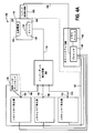
図4Aは、エッチング速度を決定するために使用される、電圧及び電流及び/若しくは電力の係数、並びに/又は電圧及び電流及び/若しくは電力の指数、並びに/又は周波数を決定するための、プラズマシステム250の一実施形態のブロック図である。プラズマシステム250は、プラズマシステム100(図2A)と、エッチング速度測定機器(ERMD)252とを含む。ERMD252は、ケーブル254を通じてプロセッサ128に接続され、プラズマチャンバ118の窓256を通る見通し線を有する。該見通し線は、プラズマチャンバ118内でプラズマが発生する空間内へ方向付けられる。例えば、ERMD252は、プラズマによって発せられて窓256を通る放射の強度を測定するために、プラズマチャンバ118内のプラズマを監視する分光光度計を含む。一部の実施形態では、窓256は、プラズマによって発せられた光が通過することを可能にする例えばガラスなどの透明材料で作成される。様々な実施形態において、窓256は、半透明窓である。強度は、プラズマによって消耗されるダミーウエハ124の層のエッチング速度に正比例する。プロセッサ128は、測定された強度をケーブル254を通じて受信し、強度に正比例するものとしてエッチング速度を決定する。別の例として、レシピが既知である場合は、ERMD252は、時刻tm1においてダミーウエハ124の厚さを測定し、時刻tm1の後で且つダミーウエハ124のエッチングの後である時刻tm2においてダミーウエハ124の厚さを測定する。ERMD252は、ダミーウエハ124のエッチング速度ER2501を、時刻tm2における厚さと時刻tm1における厚さとの差を時刻tm2と時刻tm1との差で割った比率として決定する。エッチング速度ER2501は、ケーブル254を通じてERMD252によってプロセッサ128に提供される。一部の実施形態では、ERMD252がエッチング速度ER2501を決定する代わりに、プロセッサ128が、測定された強度からエッチング速度ER2501を決定し、該エッチング速度ER2501を、記憶させるためにメモリデバイス132に提供する。既知のレシピの例は、プラズマチャンバ118内で維持される圧力、プラズマチャンバ118内で維持される温度、上部電極122とチャック120との間のギャップ、xMHzRF発生器、yMHzRF発生器、及びzMHzRF発生器によって供給される電力の大きさ、xMHzRF発生器、yMHzRF発生器、及びzMHzRF発生器の周波数、又はそれらの組み合わせを含む。
FIG. 4A illustrates a plasma system for determining voltage and current and / or power coefficients and / or voltage and current and / or power indices and / or frequencies used to determine the etch rate. 2 is a block diagram of one embodiment of 250. FIG.
上述のように、複素インピーダンスセンサ119は、複素電圧・電流の測定値をケーブル127を通じてプロセッサ128に提供する。プロセッサ128は、複素電圧・電流の測定値を受信し、該測定値から電圧振幅V3及び電流振幅I3及び/又は電力振幅P3を抽出し、これらの電圧振幅V3及び電流振幅I3及び電力振幅P3を、記憶させるためにメモリデバイス132に提供する。例えばプロセッサ128は、電力振幅P3を、電圧振幅V3と、電流振幅I3と、電圧振幅V3と電流振幅I3との間の位相であるφ3とを乗じた積として算出する。一部の実施形態では、電圧振幅V3は電圧振幅V1と同じであり、電流振幅I3は電流振幅I1と同じであり、電力振幅P3は電力振幅P1と同じであり、位相φ3はプラズマシステム100を使用して決定される位相φ1と同じである。一部の実施形態では、出力102に接続された周波数センサが、xMHzRF発生器によって供給されるRF信号の周波数F3を測定し、該周波数F3を、周波数センサをプロセッサ128に接続しているケーブルを通じてプロセッサ128に提供する。様々な実施形態において、周波数F3は、周波数F1と同じである。
As described above,
様々な実施形態において、エッチング速度ER2071を決定する代わりに、ERMD272は、プラズマチャンバ158内で発生するプラズマによって発せられる光の強度を窓273を介して測定し、該測定された強度を、ケーブル274を通じてプロセッサ128に提供する。ケーブル274は、ERMD272をプロセッサ128に接続している。一部の実施形態では、プロセッサ128は、エッチング速度ER2701を、測定された強度に正比例するものとして決定し、該エッチング速度ER2701を、記憶させるためにメモリデバイス132に提供する。
In various embodiments, instead of determining the etch rate ER 2071, the ERMD 272 measures the intensity of light emitted by the plasma generated in the plasma chamber 158 through the window 273, and the measured intensity is measured by the cable 274. To the
図5は、zMHzRF発生器が例えば電力を供給している、作動している、機能しているなどのように稼働しており、xMHzRF発生器及びyMHzRF発生器が例えば電力を供給していないなどのように稼働していないときにおける、例えば二次多項式エッチング速度、三次多項式エッチング速度、四次多項式エッチング速度などのエッチング速度モデルの平均値対ERMDを使用して決定された測定エッチング速度の平均値のグラフの一実施形態290である。ERMDを使用して決定された平均測定エッチング速度は、x軸に沿ってプロットされ、平均エッチング速度モデルは、y軸に沿ってプロットされる。グラフ290の各平均エッチング速度モデルの各点を通るように、最良適合直線が引かれてよい。図に示されるように、グラフ290における二次多項式平均エッチング速度モデルは、0.998の決定係数(R2)を有し、グラフ290における三次多項式平均エッチング速度モデルは、0.9999のR2を有し、グラフ290における四次多項式平均エッチング速度モデルは、0.9997のR2を有する。R2が大きいほど、エッチング速度モデルの平均値の正確さが増す。 FIG. 5 shows that the z MHz RF generator is operating, eg, supplying power, operating, functioning, etc., and the x MHz RF generator and the y MHz RF generator are not supplying power, etc. For example, the average value of the etching rate model determined using ERMD versus the average value of the etching rate model such as the second-order polynomial etching rate, the third-order polynomial etching rate, the fourth-order polynomial etching rate, etc. 2 is one embodiment 290 of the graph. The average measured etch rate determined using ERMD is plotted along the x-axis and the average etch rate model is plotted along the y-axis. A best-fit line may be drawn through each point of each average etch rate model in graph 290. As shown, the second order polynomial average etch rate model in graph 290 has a coefficient of determination (R 2 ) of 0.998 , and the third order polynomial average etch rate model in graph 290 is an R 2 of 0.9999. And the fourth order polynomial average etch rate model in graph 290 has an R 2 of 0.9997. The larger R 2 is, the more accurate the average value of the etching rate model is.
Claims (23)
第1のプラズマシステムの高周波(RF)発生器の出力において測定される電圧及び電流を受信することと、
前記電圧及び電流、及び電力に基づいて、第1のモデルエッチング速度を算出することであって、前記電力は、前記電圧及び電流、及び前記電圧と前記電流との間の位相に基づいて算出される、ことと、
第2のプラズマシステムのRF発生器の出力において測定される電圧及び電流を受信することと、
前記第2のプラズマシステムの前記RF発生器の前記出力における前記電圧及び電流に基づいて、第2のモデルエッチング速度を決定することと、
前記第2のモデルエッチング速度を前記第1のモデルエッチング速度と比較することと、
前記第2のモデルエッチング速度が前記第1のモデルエッチング速度に一致しないことが決定された際に、前記第1のプラズマシステムに関係付けられた前記第1のモデルエッチング速度を実現するために、前記第2のプラズマシステムの前記RF発生器の前記出力における電力を調整することと、
を備え、
プロセッサによって実行される方法。 A method for performing chamber-to-chamber matching of etch rates based on a model etch rate comprising:
Receiving a voltage and current measured at the output of a radio frequency (RF) generator of the first plasma system;
Calculating a first model etching rate based on the voltage, current and power, wherein the power is calculated based on the voltage and current and a phase between the voltage and current; And that
Receiving the voltage and current measured at the output of the RF generator of the second plasma system;
Determining a second model etch rate based on the voltage and current at the output of the RF generator of the second plasma system;
Comparing the second model etch rate with the first model etch rate;
To achieve the first model etch rate associated with the first plasma system when it is determined that the second model etch rate does not match the first model etch rate, Adjusting the power at the output of the RF generator of the second plasma system;
With
The method performed by the processor.
前記第1のプラズマシステムに関係付けられた前記第1のモデルエッチング速度を実現するために、前記第2のプラズマシステムの前記RF発生器の前記出力における前記電圧又は電流を調整することを備える方法。 The method of claim 1, further comprising:
Adjusting the voltage or current at the output of the RF generator of the second plasma system to achieve the first model etch rate associated with the first plasma system. .
前記第1のモデルエッチング速度を算出するために使用される前記電圧及び電流は、電圧振幅、及び電流振幅、及び前記電圧振幅と前記電流振幅との間の位相を含み、前記第1のモデルエッチング速度を算出するために使用される前記電力は、電力振幅を含み、前記電力振幅は、前記電圧振幅と、前記電流振幅と、前記位相との積として算出される、方法。 The method of claim 1, comprising:
The voltage and current used to calculate the first model etch rate include a voltage amplitude, a current amplitude, and a phase between the voltage amplitude and the current amplitude, and the first model etch. The method wherein the power used to calculate velocity includes power amplitude, and the power amplitude is calculated as a product of the voltage amplitude, the current amplitude, and the phase.
前記第1のプラズマシステムの前記RF発生器の前記出力において測定される周波数を受信することと、
前記周波数に基づいて、第3のモデルエッチング速度を算出することと、
前記第2のプラズマシステムの前記RF発生器の前記出力において測定される周波数を受信することと、
前記第2のプラズマシステムの前記RF発生器の前記出力において測定される前記周波数に基づいて、第4のモデルエッチング速度を算出することと、
前記第3のモデルエッチング速度を前記第4のモデルエッチング速度と比較することと、
前記第1のプラズマシステムに関係付けられた前記第3のモデルエッチング速度を実現するために、前記第2のプラズマシステムの前記RF発生器の前記出力における前記電力を調整することと、
を備える方法。 The method of claim 1, further comprising:
Receiving a frequency measured at the output of the RF generator of the first plasma system;
Calculating a third model etch rate based on the frequency;
Receiving a frequency measured at the output of the RF generator of the second plasma system;
Calculating a fourth model etch rate based on the frequency measured at the output of the RF generator of the second plasma system;
Comparing the third model etch rate with the fourth model etch rate;
Adjusting the power at the output of the RF generator of the second plasma system to achieve the third model etch rate associated with the first plasma system;
A method comprising:
前記第1のプラズマシステムに関係付けられた前記第3のモデルエッチング速度を実現するために、前記第2のプラズマシステムの前記RF発生器の前記出力における前記周波数を調整することを備える方法。 The method of claim 4, further comprising:
Adjusting the frequency at the output of the RF generator of the second plasma system to achieve the third model etch rate associated with the first plasma system.
前記第1のプラズマシステムの前記RF発生器の前記出力において測定される前記電圧及び電流、及び前記周波数を受信することは、前記第1のプラズマシステムのプラズマチャンバ内でダミーウエハを使用して実施される、方法。 The method of claim 4, comprising:
Receiving the voltage and current measured at the output of the RF generator of the first plasma system and the frequency is performed using a dummy wafer within the plasma chamber of the first plasma system. The way.
前記第1のプラズマシステムの前記RF発生器は、ケーブルを通じてインピーダンス整合回路に接続され、前記インピーダンス整合回路は、RF伝送路を通じてプラズマチャンバに接続される、方法。 The method of claim 1, comprising:
The RF generator of the first plasma system is connected to an impedance matching circuit through a cable, and the impedance matching circuit is connected to the plasma chamber through an RF transmission line.
前記第1のプラズマシステムの前記RF発生器の前記出力は、インピーダンス整合回路の入力に接続され、前記出力は、前記インピーダンス整合回路を通じてプラズマチャンバにRF信号を送ることを促すために使用される、方法。 The method of claim 1, comprising:
The output of the RF generator of the first plasma system is connected to an input of an impedance matching circuit, and the output is used to facilitate sending an RF signal to the plasma chamber through the impedance matching circuit; Method.
前記第2のプラズマシステムの前記RF発生器の前記出力における前記電力を調整することは、前記第2のプラズマシステムが半導体ウエハをエッチングするために使用されるときに実施される、方法。 The method of claim 1, comprising:
The method wherein adjusting the power at the output of the RF generator of the second plasma system is performed when the second plasma system is used to etch a semiconductor wafer.
前記電力を調整することは、前記第2のプラズマシステムの前記RF発生器の前記出力において測定される前記電力を引き上げる又は引き下げることを含む、方法。 The method of claim 1, comprising:
Adjusting the power includes raising or lowering the power measured at the output of the RF generator of the second plasma system.
前記第1のプラズマシステムは、前記第2のプラズマシステムのツールと機能的に同一であって前記第2のプラズマシステムの前記ツールと異なる識別情報を有するツールを含む、方法。 The method of claim 1, comprising:
The first plasma system includes a tool that is functionally identical to a tool of the second plasma system and has identification information different from the tool of the second plasma system.
前記第1のプラズマシステムは、前記第2のプラズマシステムのツールと構造的に同一であって前記第2のプラズマシステムの前記ツールと異なる識別情報を有するツールを含む、方法。 The method of claim 1, comprising:
The method of claim 1, wherein the first plasma system includes a tool that is structurally identical to the tool of the second plasma system and has identification information different from the tool of the second plasma system.
前記第1のプラズマシステムは、前記第2のプラズマシステムのツールと構造的に及び機能的に同一であって前記第2のプラズマシステムの前記ツールと異なる識別情報を有するツールを含む、方法。 The method of claim 1, comprising:
The first plasma system includes a tool that is structurally and functionally identical to a tool of the second plasma system and has identification information different from the tool of the second plasma system.
前記第1のモデルエッチング速度を算出することは、テイラー級数である和を算出することを含む、方法。 The method of claim 1, comprising:
The calculating the first model etch rate includes calculating a sum that is a Taylor series.
プラズマシステムの高周波(RF)発生器の出力において第1の時点において測定される電圧及び電流を受信することと、
前記電圧、前記電流、及び電力に基づいて、第1のモデルエッチング速度を算出することであって、前記電力は、前記電圧と前記電流との間の位相に基づいて算出される、ことと、
前記RF発生器の前記出力において第2の時点において測定される電圧及び電流を受信することと、
前記第2の時点で測定される前記電圧、前記第2の時点で測定される前記電流、及び電力に基づいて、第2のモデルエッチング速度を算出することであって、前記電力は、前記第2の時点において測定される前記電圧と前記電流との間の位相に基づいて算出される、ことと、
前記第1のモデルエッチング速度を前記第2のモデルエッチング速度と比較することと、
前記第2のモデルエッチング速度が前記第1のモデルエッチング速度に一致しないことが決定された際に、前記第1のモデルエッチング速度を実現するために、前記RF発生器の前記出力における電力を調整することと、
を備え、
プロセッサによって実行される方法。 A method for performing in-chamber alignment of etch rates based on a model etch rate comprising:
Receiving a voltage and current measured at a first time at the output of a radio frequency (RF) generator of the plasma system;
Calculating a first model etching rate based on the voltage, the current, and the power, wherein the power is calculated based on a phase between the voltage and the current;
Receiving a voltage and current measured at a second time point at the output of the RF generator;
Calculating a second model etch rate based on the voltage measured at the second time point, the current measured at the second time point , and power, wherein the power is Calculated on the basis of the phase between the voltage and the current measured at a point of time 2;
Comparing the first model etch rate to the second model etch rate;
When it is determined that the second model etch rate does not match the first model etch rate, power at the output of the RF generator is adjusted to achieve the first model etch rate. To do
With
The method performed by the processor.
前記RF発生器の前記出力において前記第1の時点において測定される周波数を受信することと、
前記周波数に基づいて、第3のモデルエッチング速度を算出することと、
前記RF発生器の前記出力において前記第2の時点において測定される周波数を受信することと、
前記第2の時点において測定される前記周波数に基づいて、第4のモデルエッチング速度を算出することと、
前記第3のモデルエッチング速度を前記第4のモデルエッチング速度と比較することと、
前記第3のモデルエッチング速度が前記第4のモデルエッチング速度に一致しないことが決定された際に、前記第3のモデルエッチング速度を実現するために、前記RF発生器の前記出力における前記電力を調整することと、
を備える方法。 The method of claim 15, further comprising:
Receiving a frequency measured at the first time point at the output of the RF generator;
Calculating a third model etch rate based on the frequency;
Receiving a frequency measured at the second time point in the output of the RF generator,
Calculating a fourth model etch rate based on the frequency measured at the second time point;
Comparing the third model etch rate with the fourth model etch rate;
When it is determined that the third model etch rate does not match the fourth model etch rate, to achieve the third model etch rate, the power at the output of the RF generator is Adjusting,
A method comprising:
前記第3のモデルエッチング速度を実現するために、前記RF発生器の前記出力における前記電圧又は電流又は周波数を調整することを備える方法。 The method of claim 16, further comprising:
Adjusting the voltage or current or frequency at the output of the RF generator to achieve the third model etch rate.
前記RF発生器の前記出力において前記第1の時点において測定される前記電圧、前記電流、及び前記周波数を受信することは、前記プラズマシステムのプラズマチャンバ内でダミーウエハを使用して実施される、方法。 The method according to claim 16, comprising:
Receiving the voltage, the current, and the frequency measured at the first time point at the output of the RF generator is performed using a dummy wafer in a plasma chamber of the plasma system. .
前記第2の時点は、前記第1の時点の後に起きる、方法。 16. A method according to claim 15, comprising
The method, wherein the second time point occurs after the first time point.
前記第1のモデルエッチング速度を算出するために使用される前記電圧及び電流は、電圧振幅、及び電流振幅、及び前記電圧振幅と前記電流振幅との間の位相を含み、前記第1のモデルエッチング速度を算出するために使用される前記電力は、電力振幅を含む、方法。 16. A method according to claim 15, comprising
The voltage and current used to calculate the first model etch rate include a voltage amplitude, a current amplitude, and a phase between the voltage amplitude and the current amplitude, and the first model etch. The method, wherein the power used to calculate velocity includes power amplitude.
前記RF発生器の前記出力における前記電力を調整することは、前記プラズマシステムが半導体ウエハをエッチングするために使用されるときに実施される、方法。 16. A method according to claim 15, comprising
Adjusting the pre-Symbol power that put to the output of the RF generator, the plasma system is carried out when it is used to etch the semiconductor wafer, the method.
RF信号を生成するための高周波(RF)発生器であって、前記RF信号の送出を促すための出力を含むRF発生器と、
前記RF信号の電圧及び電流を測定するための、前記出力に接続された複素インピーダンスセンサと、
プラズマを発生するプラズマチャンバと、
RF信号を修正して修正RF信号を生成するための、ケーブルを通じて前記RF発生器に及びRF伝送路を通じて前記プラズマチャンバに接続されたインピーダンス整合回路と、
を備え、
前記プラズマチャンバは、前記インピーダンス整合回路から前記修正RF信号が受信されたときに前記プラズマを発生させるように構成されており、
前記第1のプラズマシステムは、更に、
前記複素インピーダンスセンサに接続されたプロセッサであって、
前記RF発生器の前記出力において測定される前記電圧及び電流を受信するためと、
前記電圧及び電流、及び電力に基づいて、第1のモデルエッチング速度を算出するためであって、前記電力は、前記電圧及び電流、及び前記電圧と前記電流との間の位相に基づいて算出される、ためと、
第2のプラズマシステムのRF発生器の出力において測定される電圧及び電流を受信することと、
前記第2のプラズマシステムの前記RF発生器の前記出力における前記電圧及び電流に基づいて、第2のモデルエッチング速度を決定するためと、
前記第2のモデルエッチング速度を前記第1のモデルエッチング速度と比較するためと、
前記第2のモデルエッチング速度が前記第1のモデルエッチング速度に一致しないことが決定された際に、前記第1のモデルエッチング速度を実現するために、前記第1のプラズマシステムの前記RF発生器の前記出力における電力を調整するためと、
である、プロセッサと、
を備える第1のプラズマシステム。 A first plasma system comprising:
A radio frequency (RF) generator for generating an RF signal, the RF generator including an output for encouraging transmission of the RF signal;
A complex impedance sensor connected to the output for measuring the voltage and current of the RF signal;
A plasma chamber for generating plasma;
An impedance matching circuit connected to the RF generator through a cable and to the plasma chamber through an RF transmission line for modifying the RF signal to generate a modified RF signal;
With
Wherein the plasma chamber, the being configured to generate a plasma when said modified RF signal from the impedance matching circuit is received,
The first plasma system further comprises:
A processor connected to the complex impedance sensor,
Receiving the voltage and current measured at the output of the RF generator;
For calculating a first model etching rate based on the voltage, current, and power, the power is calculated based on the voltage and current, and a phase between the voltage and current. For,
Receiving the voltage and current measured at the output of the RF generator of the second plasma system;
Determining a second model etch rate based on the voltage and current at the output of the RF generator of the second plasma system;
For comparing the second model etch rate with the first model etch rate;
The RF generator of the first plasma system to achieve the first model etch rate when it is determined that the second model etch rate does not match the first model etch rate. Adjusting the power at the output of
A processor,
A first plasma system comprising:
前記プロセッサは、更に、前記第1のモデルエッチング速度を実現するために、前記第1のプラズマシステムの前記RF発生器の前記出力における前記電圧又は前記電流を調整するように構成される、第1のプラズマシステム。 A first plasma system according to claim 22,
The processor is further configured to adjust the voltage or the current at the output of the RF generator of the first plasma system to achieve the first model etch rate. Plasma system.
Applications Claiming Priority (4)
| Application Number | Priority Date | Filing Date | Title |
|---|---|---|---|
| US201361858985P | 2013-07-26 | 2013-07-26 | |
| US61/858,985 | 2013-07-26 | ||
| US14/243,705 US9502221B2 (en) | 2013-07-26 | 2014-04-02 | Etch rate modeling and use thereof with multiple parameters for in-chamber and chamber-to-chamber matching |
| US14/243,705 | 2014-04-02 |
Publications (3)
| Publication Number | Publication Date |
|---|---|
| JP2015029093A JP2015029093A (en) | 2015-02-12 |
| JP2015029093A5 true JP2015029093A5 (en) | 2015-03-26 |
| JP6465579B2 JP6465579B2 (en) | 2019-02-06 |
Family
ID=52389903
Family Applications (1)
| Application Number | Title | Priority Date | Filing Date |
|---|---|---|---|
| JP2014147263A Active JP6465579B2 (en) | 2013-07-26 | 2014-07-18 | Etch rate modeling using multiple parameters and its use for intra-chamber alignment and inter-chamber alignment |
Country Status (5)
| Country | Link |
|---|---|
| US (2) | US9502221B2 (en) |
| JP (1) | JP6465579B2 (en) |
| KR (2) | KR102282713B1 (en) |
| CN (1) | CN104347340B (en) |
| TW (3) | TWI641042B (en) |
Families Citing this family (13)
| Publication number | Priority date | Publication date | Assignee | Title |
|---|---|---|---|---|
| US9720022B2 (en) | 2015-05-19 | 2017-08-01 | Lam Research Corporation | Systems and methods for providing characteristics of an impedance matching model for use with matching networks |
| US9412670B2 (en) * | 2013-05-23 | 2016-08-09 | Lam Research Corporation | System, method and apparatus for RF power compensation in plasma etch chamber |
| US9460894B2 (en) * | 2013-06-28 | 2016-10-04 | Lam Research Corporation | Controlling ion energy within a plasma chamber |
| US9595424B2 (en) * | 2015-03-02 | 2017-03-14 | Lam Research Corporation | Impedance matching circuit for operation with a kilohertz RF generator and a megahertz RF generator to control plasma processes |
| JP6604595B2 (en) * | 2016-03-10 | 2019-11-13 | パナソニックIpマネジメント株式会社 | Plasma processing apparatus and plasma processing method |
| US10438805B2 (en) | 2016-12-06 | 2019-10-08 | Tokyo Electron Limited | Methods and systems for chamber matching and monitoring |
| CN108663642B (en) * | 2017-03-31 | 2020-09-29 | 西门子(深圳)磁共振有限公司 | Tuning and detuning structure and method of radio frequency coil |
| US10636686B2 (en) * | 2018-02-27 | 2020-04-28 | Lam Research Corporation | Method monitoring chamber drift |
| JP7018823B2 (en) * | 2018-05-29 | 2022-02-14 | 東京エレクトロン株式会社 | Model generator, model generator and model generation method |
| WO2020036801A1 (en) * | 2018-08-17 | 2020-02-20 | Lam Research Corporation | Rf power compensation to reduce deposition or etch rate changes in response to substrate bulk resistivity variations |
| JP7257918B2 (en) * | 2019-08-29 | 2023-04-14 | 東京エレクトロン株式会社 | Plasma processing system and plasma ignition support method |
| CN110850812B (en) * | 2019-11-18 | 2020-07-31 | 北京邮电大学 | Ion beam etching rate control method and device based on model |
| DE102022108634A1 (en) * | 2022-04-08 | 2023-10-12 | TRUMPF Hüttinger GmbH + Co. KG | Plasma system and method for operating a plasma system |
Family Cites Families (166)
| Publication number | Priority date | Publication date | Assignee | Title |
|---|---|---|---|---|
| US4377961A (en) | 1979-09-10 | 1983-03-29 | Bode Harald E W | Fundamental frequency extracting system |
| DE3027828A1 (en) | 1980-07-23 | 1982-03-04 | Deutsche Itt Industries Gmbh, 7800 Freiburg | FREQUENCY / PHASE CONTROL LOOP |
| US4353777A (en) | 1981-04-20 | 1982-10-12 | Lfe Corporation | Selective plasma polysilicon etching |
| US4457820A (en) | 1981-12-24 | 1984-07-03 | International Business Machines Corporation | Two step plasma etching |
| US4420790A (en) | 1982-04-02 | 1983-12-13 | Honeywell Inc. | High sensitivity variable capacitance transducer |
| US4454001A (en) | 1982-08-27 | 1984-06-12 | At&T Bell Laboratories | Interferometric method and apparatus for measuring etch rate and fabricating devices |
| US4500563A (en) | 1982-12-15 | 1985-02-19 | Pacific Western Systems, Inc. | Independently variably controlled pulsed R.F. plasma chemical vapor processing |
| US4855897A (en) | 1987-07-13 | 1989-08-08 | The Foxboro Company | Method and apparatus for statistical set point bias control |
| DE3923662A1 (en) | 1989-07-18 | 1991-01-24 | Leybold Ag | CIRCUIT ARRANGEMENT FOR AUTOMATICALLY TUNING A ADAPTATION NETWORK |
| US5788801A (en) | 1992-12-04 | 1998-08-04 | International Business Machines Corporation | Real time measurement of etch rate during a chemical etching process |
| US5479340A (en) | 1993-09-20 | 1995-12-26 | Sematech, Inc. | Real time control of plasma etch utilizing multivariate statistical analysis |
| US5571366A (en) | 1993-10-20 | 1996-11-05 | Tokyo Electron Limited | Plasma processing apparatus |
| US5980767A (en) | 1994-02-25 | 1999-11-09 | Tokyo Electron Limited | Method and devices for detecting the end point of plasma process |
| US5556549A (en) | 1994-05-02 | 1996-09-17 | Lsi Logic Corporation | Power control and delivery in plasma processing equipment |
| US5474648A (en) | 1994-07-29 | 1995-12-12 | Lsi Logic Corporation | Uniform and repeatable plasma processing |
| US5989999A (en) | 1994-11-14 | 1999-11-23 | Applied Materials, Inc. | Construction of a tantalum nitride film on a semiconductor wafer |
| US6042686A (en) | 1995-06-30 | 2000-03-28 | Lam Research Corporation | Power segmented electrode |
| US5810963A (en) | 1995-09-28 | 1998-09-22 | Kabushiki Kaisha Toshiba | Plasma processing apparatus and method |
| US5892198A (en) | 1996-03-29 | 1999-04-06 | Lam Research Corporation | Method of and apparatus for electronically controlling r.f. energy supplied to a vacuum plasma processor and memory for same |
| US5812361A (en) | 1996-03-29 | 1998-09-22 | Lam Research Corporation | Dynamic feedback electrostatic wafer chuck |
| US6110214A (en) | 1996-05-03 | 2000-08-29 | Aspen Technology, Inc. | Analyzer for modeling and optimizing maintenance operations |
| US5764471A (en) | 1996-05-08 | 1998-06-09 | Applied Materials, Inc. | Method and apparatus for balancing an electrostatic force produced by an electrostatic chuck |
| US5689215A (en) | 1996-05-23 | 1997-11-18 | Lam Research Corporation | Method of and apparatus for controlling reactive impedances of a matching network connected between an RF source and an RF plasma processor |
| US6048435A (en) | 1996-07-03 | 2000-04-11 | Tegal Corporation | Plasma etch reactor and method for emerging films |
| US6246972B1 (en) | 1996-08-23 | 2001-06-12 | Aspen Technology, Inc. | Analyzer for modeling and optimizing maintenance operations |
| JP3630931B2 (en) * | 1996-08-29 | 2005-03-23 | 富士通株式会社 | Plasma processing apparatus, process monitoring method, and semiconductor device manufacturing method |
| US5737177A (en) | 1996-10-17 | 1998-04-07 | Applied Materials, Inc. | Apparatus and method for actively controlling the DC potential of a cathode pedestal |
| US5866985A (en) | 1996-12-03 | 1999-02-02 | International Business Machines Corporation | Stable matching networks for plasma tools |
| US5694207A (en) | 1996-12-09 | 1997-12-02 | Taiwan Semiconductor Manufacturing Company, Ltd. | Etch rate monitoring by optical emission spectroscopy |
| US5889252A (en) | 1996-12-19 | 1999-03-30 | Lam Research Corporation | Method of and apparatus for independently controlling electric parameters of an impedance matching network |
| US6017414A (en) * | 1997-03-31 | 2000-01-25 | Lam Research Corporation | Method of and apparatus for detecting and controlling in situ cleaning time of vacuum processing chambers |
| US5894400A (en) | 1997-05-29 | 1999-04-13 | Wj Semiconductor Equipment Group, Inc. | Method and apparatus for clamping a substrate |
| US6351683B1 (en) | 1997-09-17 | 2002-02-26 | Tokyo Electron Limited | System and method for monitoring and controlling gas plasma processes |
| US6020794A (en) | 1998-02-09 | 2000-02-01 | Eni Technologies, Inc. | Ratiometric autotuning algorithm for RF plasma generator |
| US6157867A (en) | 1998-02-27 | 2000-12-05 | Taiwan Semiconductor Manufacturing Company | Method and system for on-line monitoring plasma chamber condition by comparing intensity of certain wavelength |
| US6198616B1 (en) | 1998-04-03 | 2001-03-06 | Applied Materials, Inc. | Method and apparatus for supplying a chucking voltage to an electrostatic chuck within a semiconductor wafer processing system |
| EP1098359A4 (en) | 1998-06-02 | 2003-11-19 | Nikon Corp | Scanning aligner, method of manufacture thereof, and method of manufacturing device |
| US6021672A (en) | 1998-09-18 | 2000-02-08 | Windbond Electronics Corp. | Simultaneous in-situ optical sensing of pressure and etch rate in plasma etch chamber |
| JP4408313B2 (en) | 1999-10-29 | 2010-02-03 | 東京エレクトロン株式会社 | Plasma processing apparatus and plasma processing method |
| US7361287B2 (en) | 1999-04-30 | 2008-04-22 | Robert Bosch Gmbh | Method for etching structures in an etching body by means of a plasma |
| US6431112B1 (en) | 1999-06-15 | 2002-08-13 | Tokyo Electron Limited | Apparatus and method for plasma processing of a substrate utilizing an electrostatic chuck |
| US6319355B1 (en) * | 1999-06-30 | 2001-11-20 | Lam Research Corporation | Plasma processor with coil responsive to variable amplitude rf envelope |
| US6528751B1 (en) | 2000-03-17 | 2003-03-04 | Applied Materials, Inc. | Plasma reactor with overhead RF electrode tuned to the plasma |
| US6441555B1 (en) | 2000-03-31 | 2002-08-27 | Lam Research Corporation | Plasma excitation coil |
| US6472822B1 (en) | 2000-04-28 | 2002-10-29 | Applied Materials, Inc. | Pulsed RF power delivery for plasma processing |
| US7137354B2 (en) | 2000-08-11 | 2006-11-21 | Applied Materials, Inc. | Plasma immersion ion implantation apparatus including a plasma source having low dissociation and low minimum plasma voltage |
| JP4240259B2 (en) | 2000-08-21 | 2009-03-18 | 富士電機システムズ株式会社 | Plasma potential measurement method and measurement probe |
| US6492774B1 (en) | 2000-10-04 | 2002-12-10 | Lam Research Corporation | Wafer area pressure control for plasma confinement |
| US7871676B2 (en) | 2000-12-06 | 2011-01-18 | Novellus Systems, Inc. | System for depositing a film by modulated ion-induced atomic layer deposition (MII-ALD) |
| JP4270872B2 (en) | 2001-03-16 | 2009-06-03 | 東京エレクトロン株式会社 | System and method for monitoring impedance |
| US6522121B2 (en) | 2001-03-20 | 2003-02-18 | Eni Technology, Inc. | Broadband design of a probe analysis system |
| IE20010288A1 (en) | 2001-03-23 | 2002-10-02 | Scient Systems Res Ltd | Endpoint Detection in the Etching of Dielectric Layers |
| US7096819B2 (en) | 2001-03-30 | 2006-08-29 | Lam Research Corporation | Inductive plasma processor having coil with plural windings and method of controlling plasma density |
| US6750711B2 (en) | 2001-04-13 | 2004-06-15 | Eni Technology, Inc. | RF power amplifier stability |
| US6669783B2 (en) | 2001-06-28 | 2003-12-30 | Lam Research Corporation | High temperature electrostatic chuck |
| US6727655B2 (en) | 2001-10-26 | 2004-04-27 | Mcchesney Jon | Method and apparatus to monitor electrical states at a workpiece in a semiconductor processing chamber |
| JP4006982B2 (en) | 2001-11-16 | 2007-11-14 | セイコーエプソン株式会社 | Printer and printer unit |
| KR100557842B1 (en) | 2001-12-10 | 2006-03-10 | 동경 엘렉트론 주식회사 | High-frequency power source and its control method, and plasma processor |
| US20030119308A1 (en) | 2001-12-20 | 2003-06-26 | Geefay Frank S. | Sloped via contacts |
| US7480571B2 (en) | 2002-03-08 | 2009-01-20 | Lam Research Corporation | Apparatus and methods for improving the stability of RF power delivery to a plasma load |
| US6962644B2 (en) * | 2002-03-18 | 2005-11-08 | Applied Materials, Inc. | Tandem etch chamber plasma processing system |
| JP2003282545A (en) | 2002-03-26 | 2003-10-03 | Seiko Epson Corp | Method of manufacturing semiconductor device and plasma treatment apparatus |
| US7557591B2 (en) | 2002-03-28 | 2009-07-07 | Tokyo Electron Limited | System and method for determining the state of a film in a plasma reactor using an electrical property |
| US7505879B2 (en) | 2002-06-05 | 2009-03-17 | Tokyo Electron Limited | Method for generating multivariate analysis model expression for processing apparatus, method for executing multivariate analysis of processing apparatus, control device of processing apparatus and control system for processing apparatus |
| AU2003245315A1 (en) | 2002-06-28 | 2004-01-19 | Tokyo Electron Limited | Method and system for predicting process performance using material processing tool and sensor data |
| US20040028837A1 (en) | 2002-06-28 | 2004-02-12 | Tokyo Electron Limited | Method and apparatus for plasma processing |
| US6664166B1 (en) | 2002-09-13 | 2003-12-16 | Texas Instruments Incorporated | Control of nichorme resistor temperature coefficient using RF plasma sputter etch |
| US6873114B2 (en) | 2002-09-26 | 2005-03-29 | Lam Research Corporation | Method for toolmatching and troubleshooting a plasma processing system |
| US20040060660A1 (en) | 2002-09-26 | 2004-04-01 | Lam Research Inc., A Delaware Corporation | Control of plasma density with broadband RF sensor |
| KR100708313B1 (en) * | 2002-10-31 | 2007-04-17 | 세메스 주식회사 | Apparatus and method for treating plasma |
| TW201041455A (en) | 2002-12-16 | 2010-11-16 | Japan Science & Tech Agency | Plasma generation device, plasma control method, and substrate manufacturing method |
| US20040127031A1 (en) | 2002-12-31 | 2004-07-01 | Tokyo Electron Limited | Method and apparatus for monitoring a plasma in a material processing system |
| JP2004239211A (en) | 2003-02-07 | 2004-08-26 | Denso Corp | Intake module |
| US6781317B1 (en) | 2003-02-24 | 2004-08-24 | Applied Science And Technology, Inc. | Methods and apparatus for calibration and metrology for an integrated RF generator system |
| JP2004335594A (en) | 2003-05-02 | 2004-11-25 | Matsushita Electric Ind Co Ltd | Plasma processing device |
| US7247218B2 (en) | 2003-05-16 | 2007-07-24 | Applied Materials, Inc. | Plasma density, energy and etch rate measurements at bias power input and real time feedback control of plasma source and bias power |
| US7795153B2 (en) | 2003-05-16 | 2010-09-14 | Applied Materials, Inc. | Method of controlling a chamber based upon predetermined concurrent behavior of selected plasma parameters as a function of selected chamber parameters |
| US6862557B2 (en) | 2003-06-12 | 2005-03-01 | Lam Research Corporation | System and method for electronically collecting data in a fabrication facility |
| US7169625B2 (en) | 2003-07-25 | 2007-01-30 | Applied Materials, Inc. | Method for automatic determination of semiconductor plasma chamber matching and source of fault by comprehensive plasma monitoring |
| US7625460B2 (en) | 2003-08-01 | 2009-12-01 | Micron Technology, Inc. | Multifrequency plasma reactor |
| US7405521B2 (en) | 2003-08-22 | 2008-07-29 | Lam Research Corporation | Multiple frequency plasma processor method and apparatus |
| US8296687B2 (en) * | 2003-09-30 | 2012-10-23 | Tokyo Electron Limited | System and method for using first-principles simulation to analyze a process performed by a semiconductor processing tool |
| US7042311B1 (en) | 2003-10-10 | 2006-05-09 | Novellus Systems, Inc. | RF delivery configuration in a plasma processing system |
| JP2005130198A (en) | 2003-10-23 | 2005-05-19 | Ulvac Japan Ltd | High frequency device |
| US7838430B2 (en) | 2003-10-28 | 2010-11-23 | Applied Materials, Inc. | Plasma control using dual cathode frequency mixing |
| JP3768999B2 (en) | 2003-10-29 | 2006-04-19 | 澄英 池之内 | Plasma processing apparatus and control method thereof |
| US7190119B2 (en) | 2003-11-07 | 2007-03-13 | Lam Research Corporation | Methods and apparatus for optimizing a substrate in a plasma processing system |
| US6983215B2 (en) | 2003-12-02 | 2006-01-03 | Mks Instruments, Inc. | RF metrology characterization for field installation and serviceability for the plasma processing industry |
| US20050130620A1 (en) * | 2003-12-16 | 2005-06-16 | Andreas Fischer | Segmented radio frequency electrode apparatus and method for uniformity control |
| US7879185B2 (en) | 2003-12-18 | 2011-02-01 | Applied Materials, Inc. | Dual frequency RF match |
| US7157857B2 (en) | 2003-12-19 | 2007-01-02 | Advanced Energy Industries, Inc. | Stabilizing plasma and generator interactions |
| US6972524B1 (en) | 2004-03-24 | 2005-12-06 | Lam Research Corporation | Plasma processing system control |
| JP2005284046A (en) | 2004-03-30 | 2005-10-13 | Kumamoto Univ | Method for detecting pattern displacement and exposure device |
| US7435926B2 (en) | 2004-03-31 | 2008-10-14 | Lam Research Corporation | Methods and array for creating a mathematical model of a plasma processing system |
| US20050241762A1 (en) | 2004-04-30 | 2005-11-03 | Applied Materials, Inc. | Alternating asymmetrical plasma generation in a process chamber |
| JP2005333075A (en) * | 2004-05-21 | 2005-12-02 | Tokyo Electron Ltd | Processing method of workpiece and its processing system device |
| KR101144018B1 (en) | 2004-05-28 | 2012-05-09 | 램 리써치 코포레이션 | Plasma processor with electrode responsive to multiple rf frequencies |
| JP2006019442A (en) * | 2004-06-30 | 2006-01-19 | Fujitsu Ltd | Dry etching device and manufacturing method of semiconductor apparatus |
| FR2875304B1 (en) | 2004-09-16 | 2006-12-22 | Ecole Polytechnique Etablissem | PROBE OF MEASUREMENT OF CHARACTERISTICS OF A PLASMA EXCITATION CURRENT, AND ASSOCIATED PLASMA REACTOR |
| US20060065631A1 (en) | 2004-09-27 | 2006-03-30 | Chia-Cheng Cheng | Methods and apparatus for monitoring a process in a plasma processing system by measuring impedance |
| US20060065632A1 (en) | 2004-09-27 | 2006-03-30 | Chia-Cheng Cheng | Methods and apparatus for monitoring a process in a plasma processing system by measuring a plasma frequency |
| US7323116B2 (en) | 2004-09-27 | 2008-01-29 | Lam Research Corporation | Methods and apparatus for monitoring a process in a plasma processing system by measuring self-bias voltage |
| US7666464B2 (en) | 2004-10-23 | 2010-02-23 | Applied Materials, Inc. | RF measurement feedback control and diagnostics for a plasma immersion ion implantation reactor |
| US20060100824A1 (en) | 2004-10-27 | 2006-05-11 | Tokyo Electron Limited | Plasma processing apparatus, abnormal discharge detecting method for the same, program for implementing the method, and storage medium storing the program |
| US7459100B2 (en) | 2004-12-22 | 2008-12-02 | Lam Research Corporation | Methods and apparatus for sequentially alternating among plasma processes in order to optimize a substrate |
| US7364623B2 (en) | 2005-01-27 | 2008-04-29 | Lam Research Corporation | Confinement ring drive |
| US20060172536A1 (en) | 2005-02-03 | 2006-08-03 | Brown Karl M | Apparatus for plasma-enhanced physical vapor deposition of copper with RF source power applied through the workpiece |
| US7602127B2 (en) | 2005-04-18 | 2009-10-13 | Mks Instruments, Inc. | Phase and frequency control of a radio frequency generator from an external source |
| US7359177B2 (en) | 2005-05-10 | 2008-04-15 | Applied Materials, Inc. | Dual bias frequency plasma reactor with feedback control of E.S.C. voltage using wafer voltage measurement at the bias supply output |
| US20070021935A1 (en) | 2005-07-12 | 2007-01-25 | Larson Dean J | Methods for verifying gas flow rates from a gas supply system into a plasma processing chamber |
| US7375038B2 (en) | 2005-09-28 | 2008-05-20 | Applied Materials, Inc. | Method for plasma etching a chromium layer through a carbon hard mask suitable for photomask fabrication |
| US20080179948A1 (en) | 2005-10-31 | 2008-07-31 | Mks Instruments, Inc. | Radio frequency power delivery system |
| US7764140B2 (en) | 2005-10-31 | 2010-07-27 | Mks Instruments, Inc. | Radio frequency power delivery system |
| US7780864B2 (en) | 2006-04-24 | 2010-08-24 | Applied Materials, Inc. | Process using combined capacitively and inductively coupled plasma sources for controlling plasma ion radial distribution |
| US7722778B2 (en) | 2006-06-28 | 2010-05-25 | Lam Research Corporation | Methods and apparatus for sensing unconfinement in a plasma processing chamber |
| CN100530529C (en) | 2006-07-17 | 2009-08-19 | 应用材料公司 | Double offset frequency plasma body reactor with electrostatic chuck voltage feedback control |
| US20080029385A1 (en) | 2006-08-03 | 2008-02-07 | Tokyo Electron Limited | Plasma processing apparatus and plasma processing method |
| US7732728B2 (en) | 2007-01-17 | 2010-06-08 | Lam Research Corporation | Apparatuses for adjusting electrode gap in capacitively-coupled RF plasma reactor |
| US7858898B2 (en) | 2007-01-26 | 2010-12-28 | Lam Research Corporation | Bevel etcher with gap control |
| JP2010518597A (en) * | 2007-02-02 | 2010-05-27 | レクサス リサーチ リミテッド | Method and apparatus for determining process parameters of a plasma etching process |
| US7728602B2 (en) | 2007-02-16 | 2010-06-01 | Mks Instruments, Inc. | Harmonic derived arc detector |
| US8241457B2 (en) | 2007-03-30 | 2012-08-14 | Tokyo Electron Limited | Plasma processing system, plasma measurement system, plasma measurement method, and plasma control system |
| KR100870121B1 (en) | 2007-04-19 | 2008-11-25 | 주식회사 플라즈마트 | Impedance Matching Methods And Systems Performing The Same |
| US7768269B2 (en) | 2007-08-15 | 2010-08-03 | Applied Materials, Inc. | Method of multi-location ARC sensing with adaptive threshold comparison |
| WO2009060213A1 (en) | 2007-11-06 | 2009-05-14 | Microoncology Limited | Microwave plasms sterilisation system and applicators therefor |
| US9074285B2 (en) | 2007-12-13 | 2015-07-07 | Lam Research Corporation | Systems for detecting unconfined-plasma events |
| US7586100B2 (en) | 2008-02-12 | 2009-09-08 | Varian Semiconductor Equipment Associates, Inc. | Closed loop control and process optimization in plasma doping processes using a time of flight ion detector |
| US9856558B2 (en) * | 2008-03-14 | 2018-01-02 | Applied Materials, Inc. | Physical vapor deposition method with a source of isotropic ion velocity distribution at the wafer surface |
| JP5319150B2 (en) | 2008-03-31 | 2013-10-16 | 東京エレクトロン株式会社 | Plasma processing apparatus, plasma processing method, and computer-readable storage medium |
| KR20150017389A (en) | 2008-05-14 | 2015-02-16 | 어플라이드 머티어리얼스, 인코포레이티드 | Method and apparatus for pulsed plasma processing using a time resolved tuning scheme for rf power delivery |
| US7967944B2 (en) | 2008-05-29 | 2011-06-28 | Applied Materials, Inc. | Method of plasma load impedance tuning by modulation of an unmatched low power RF generator |
| US8337661B2 (en) | 2008-05-29 | 2012-12-25 | Applied Materials, Inc. | Plasma reactor with plasma load impedance tuning for engineered transients by synchronized modulation of an unmatched low power RF generator |
| US8264238B1 (en) | 2008-06-13 | 2012-09-11 | Mks Instruments, Inc. | Method for calibrating a broadband voltage/current probe |
| US20090308734A1 (en) | 2008-06-17 | 2009-12-17 | Schneider Automation Inc. | Apparatus and Method for Wafer Level Arc Detection |
| JP5089513B2 (en) * | 2008-07-11 | 2012-12-05 | 東京エレクトロン株式会社 | Control device for plasma processing apparatus system, control method for plasma processing system, and storage medium storing control program |
| US8103492B2 (en) | 2008-09-05 | 2012-01-24 | Tokyo Electron Limited | Plasma fluid modeling with transient to stochastic transformation |
| CN102160155A (en) | 2008-09-22 | 2011-08-17 | 应用材料公司 | Etch reactor suitable for etching high aspect ratio features |
| US8313664B2 (en) | 2008-11-21 | 2012-11-20 | Applied Materials, Inc. | Efficient and accurate method for real-time prediction of the self-bias voltage of a wafer and feedback control of ESC voltage in plasma processing chamber |
| US8040068B2 (en) | 2009-02-05 | 2011-10-18 | Mks Instruments, Inc. | Radio frequency power control system |
| US8368308B2 (en) | 2009-03-05 | 2013-02-05 | Applied Materials, Inc. | Inductively coupled plasma reactor having RF phase control and methods of use thereof |
| US8382999B2 (en) | 2009-03-26 | 2013-02-26 | Applied Materials, Inc. | Pulsed plasma high aspect ratio dielectric process |
| JP2010250959A (en) | 2009-04-10 | 2010-11-04 | Hitachi High-Technologies Corp | Plasma processing system |
| US8674606B2 (en) | 2009-04-27 | 2014-03-18 | Advanced Energy Industries, Inc. | Detecting and preventing instabilities in plasma processes |
| US8473089B2 (en) | 2009-06-30 | 2013-06-25 | Lam Research Corporation | Methods and apparatus for predictive preventive maintenance of processing chambers |
| CN102804929B (en) | 2009-06-30 | 2015-11-25 | 朗姆研究公司 | For the treatment of the method and apparatus of the predictability preventive maintenance of room |
| US8271121B2 (en) | 2009-06-30 | 2012-09-18 | Lam Research Corporation | Methods and arrangements for in-situ process monitoring and control for plasma processing tools |
| US8404598B2 (en) | 2009-08-07 | 2013-03-26 | Applied Materials, Inc. | Synchronized radio frequency pulsing for plasma etching |
| US20110097901A1 (en) | 2009-10-26 | 2011-04-28 | Applied Materials, Inc. | Dual mode inductively coupled plasma reactor with adjustable phase coil assembly |
| US8901935B2 (en) | 2009-11-19 | 2014-12-02 | Lam Research Corporation | Methods and apparatus for detecting the confinement state of plasma in a plasma processing system |
| US8501631B2 (en) | 2009-11-19 | 2013-08-06 | Lam Research Corporation | Plasma processing system control based on RF voltage |
| SG10201406954SA (en) | 2009-11-19 | 2014-11-27 | Lam Res Corp | Methods and apparatus for controlling a plasma processing system |
| US20110139748A1 (en) | 2009-12-15 | 2011-06-16 | University Of Houston | Atomic layer etching with pulsed plasmas |
| US20120000887A1 (en) | 2010-06-30 | 2012-01-05 | Kabushiki Kaisha Toshiba | Plasma treatment apparatus and plasma treatment method |
| KR20120022251A (en) | 2010-09-01 | 2012-03-12 | 삼성전자주식회사 | Plasma etching method and apparatus thereof |
| US9076826B2 (en) | 2010-09-24 | 2015-07-07 | Lam Research Corporation | Plasma confinement ring assembly for plasma processing chambers |
| US8779662B2 (en) | 2010-10-20 | 2014-07-15 | Comet Technologies Usa, Inc | Pulse mode capability for operation of an RF/VHF impedance matching network with 4 quadrant, VRMS/IRMS responding detector circuitry |
| US8723423B2 (en) | 2011-01-25 | 2014-05-13 | Advanced Energy Industries, Inc. | Electrostatic remote plasma source |
| US8679358B2 (en) | 2011-03-03 | 2014-03-25 | Tokyo Electron Limited | Plasma etching method and computer-readable storage medium |
| US9907908B2 (en) | 2011-03-08 | 2018-03-06 | Baxter International Inc. | Non-invasive radio frequency medical fluid level and volume detection system and method |
| US20130122711A1 (en) | 2011-11-10 | 2013-05-16 | Alexei Marakhtanov | System, method and apparatus for plasma sheath voltage control |
| US9224618B2 (en) | 2012-01-17 | 2015-12-29 | Lam Research Corporation | Method to increase mask selectivity in ultra-high aspect ratio etches |
| US10157729B2 (en) | 2012-02-22 | 2018-12-18 | Lam Research Corporation | Soft pulsing |
| US9210790B2 (en) | 2012-08-28 | 2015-12-08 | Advanced Energy Industries, Inc. | Systems and methods for calibrating a switched mode ion energy distribution system |
| US9408288B2 (en) | 2012-09-14 | 2016-08-02 | Lam Research Corporation | Edge ramping |
| KR102048959B1 (en) | 2012-10-30 | 2019-11-27 | 레르 리키드 쏘시에떼 아노님 뿌르 레?드 에렉스뿔라따시옹 데 프로세데 조르즈 클로드 | Method and etching gas for etching silicon-containing films |
| US9460894B2 (en) | 2013-06-28 | 2016-10-04 | Lam Research Corporation | Controlling ion energy within a plasma chamber |
-
2014
- 2014-04-02 US US14/243,705 patent/US9502221B2/en active Active
- 2014-06-27 US US14/317,360 patent/US9082594B2/en active Active
- 2014-07-18 JP JP2014147263A patent/JP6465579B2/en active Active
- 2014-07-24 TW TW103125354A patent/TWI641042B/en active
- 2014-07-25 TW TW107103421A patent/TWI654681B/en active
- 2014-07-25 TW TW103125516A patent/TWI623035B/en active
- 2014-07-25 KR KR1020140094966A patent/KR102282713B1/en active IP Right Grant
- 2014-07-28 KR KR1020140096071A patent/KR102208578B1/en active IP Right Grant
- 2014-07-28 CN CN201410363403.2A patent/CN104347340B/en active Active
Similar Documents
| Publication | Publication Date | Title |
|---|---|---|
| JP2015029093A5 (en) | ||
| US10629413B2 (en) | Adjustment of power and frequency based on three or more states | |
| KR102282713B1 (en) | Etch rate modeling and use thereof for in-chamber and chamber-to-chamber matching | |
| KR100612736B1 (en) | Plasma processing method and apparatus | |
| US8368308B2 (en) | Inductively coupled plasma reactor having RF phase control and methods of use thereof | |
| JP6312405B2 (en) | Plasma processing equipment | |
| TW201724920A (en) | RF power delivery regulation for processing substrates | |
| US9620334B2 (en) | Control of etch rate using modeling, feedback and impedance match | |
| TWI609606B (en) | Chamber matching for power control mode | |
| JP2008515198A5 (en) | ||
| TWI612854B (en) | Radiofrequency adjustment for instability mangement in semiconductor processing | |
| US20100276391A1 (en) | Inductively coupled plasma reactor having rf phase control and methods of use thereof | |
| TWI639182B (en) | System, method and apparatus for rf power compensation in plasma etch chamber | |
| JP2018107202A (en) | Plasma processing apparatus and plasma control method | |
| JP2006274420A (en) | Plasma film deposition method, and plasma cvd apparatus | |
| US9406540B2 (en) | Self-bias calculation on a substrate in a process chamber with bias power for single or multiple frequencies | |
| KR101068874B1 (en) | Apparatus for plasma processing for substrate | |
| KR102080109B1 (en) | Method of controlling of substrate processing apparatus | |
| JP2005011858A (en) | METHOD OF SETTING mu WAVE POWER IN MANUFACTURE OF SEMICONDUCTOR BY USE OF PLASMA, EQUIPMENT FOR MANUFACTURING SEMICONDUCTOR DEVICE USING THE SETTING METHOD, AND METHOD OF MANUFACTURING SEMICONDUCTOR DEVICE USING THE SETTING METHOD | |
| JP2016086040A (en) | Output inspection method of semiconductor manufacturing apparatus and semiconductor manufacturing apparatus |