JP2015007739A - Display divice and control method thereof - Google Patents
Display divice and control method thereof Download PDFInfo
- Publication number
- JP2015007739A JP2015007739A JP2013182851A JP2013182851A JP2015007739A JP 2015007739 A JP2015007739 A JP 2015007739A JP 2013182851 A JP2013182851 A JP 2013182851A JP 2013182851 A JP2013182851 A JP 2013182851A JP 2015007739 A JP2015007739 A JP 2015007739A
- Authority
- JP
- Japan
- Prior art keywords
- pixel
- value
- image data
- unit
- limited
- Prior art date
- Legal status (The legal status is an assumption and is not a legal conclusion. Google has not performed a legal analysis and makes no representation as to the accuracy of the status listed.)
- Pending
Links
Images


Classifications
-
- G—PHYSICS
- G09—EDUCATION; CRYPTOGRAPHY; DISPLAY; ADVERTISING; SEALS
- G09G—ARRANGEMENTS OR CIRCUITS FOR CONTROL OF INDICATING DEVICES USING STATIC MEANS TO PRESENT VARIABLE INFORMATION
- G09G3/00—Control arrangements or circuits, of interest only in connection with visual indicators other than cathode-ray tubes
- G09G3/20—Control arrangements or circuits, of interest only in connection with visual indicators other than cathode-ray tubes for presentation of an assembly of a number of characters, e.g. a page, by composing the assembly by combination of individual elements arranged in a matrix no fixed position being assigned to or needed to be assigned to the individual characters or partial characters
- G09G3/34—Control arrangements or circuits, of interest only in connection with visual indicators other than cathode-ray tubes for presentation of an assembly of a number of characters, e.g. a page, by composing the assembly by combination of individual elements arranged in a matrix no fixed position being assigned to or needed to be assigned to the individual characters or partial characters by control of light from an independent source
- G09G3/36—Control arrangements or circuits, of interest only in connection with visual indicators other than cathode-ray tubes for presentation of an assembly of a number of characters, e.g. a page, by composing the assembly by combination of individual elements arranged in a matrix no fixed position being assigned to or needed to be assigned to the individual characters or partial characters by control of light from an independent source using liquid crystals
- G09G3/3607—Control arrangements or circuits, of interest only in connection with visual indicators other than cathode-ray tubes for presentation of an assembly of a number of characters, e.g. a page, by composing the assembly by combination of individual elements arranged in a matrix no fixed position being assigned to or needed to be assigned to the individual characters or partial characters by control of light from an independent source using liquid crystals for displaying colours or for displaying grey scales with a specific pixel layout, e.g. using sub-pixels
-
- G—PHYSICS
- G09—EDUCATION; CRYPTOGRAPHY; DISPLAY; ADVERTISING; SEALS
- G09G—ARRANGEMENTS OR CIRCUITS FOR CONTROL OF INDICATING DEVICES USING STATIC MEANS TO PRESENT VARIABLE INFORMATION
- G09G3/00—Control arrangements or circuits, of interest only in connection with visual indicators other than cathode-ray tubes
- G09G3/20—Control arrangements or circuits, of interest only in connection with visual indicators other than cathode-ray tubes for presentation of an assembly of a number of characters, e.g. a page, by composing the assembly by combination of individual elements arranged in a matrix no fixed position being assigned to or needed to be assigned to the individual characters or partial characters
- G09G3/34—Control arrangements or circuits, of interest only in connection with visual indicators other than cathode-ray tubes for presentation of an assembly of a number of characters, e.g. a page, by composing the assembly by combination of individual elements arranged in a matrix no fixed position being assigned to or needed to be assigned to the individual characters or partial characters by control of light from an independent source
- G09G3/3406—Control of illumination source
- G09G3/342—Control of illumination source using several illumination sources separately controlled corresponding to different display panel areas, e.g. along one dimension such as lines
- G09G3/3426—Control of illumination source using several illumination sources separately controlled corresponding to different display panel areas, e.g. along one dimension such as lines the different display panel areas being distributed in two dimensions, e.g. matrix
-
- G—PHYSICS
- G09—EDUCATION; CRYPTOGRAPHY; DISPLAY; ADVERTISING; SEALS
- G09G—ARRANGEMENTS OR CIRCUITS FOR CONTROL OF INDICATING DEVICES USING STATIC MEANS TO PRESENT VARIABLE INFORMATION
- G09G2320/00—Control of display operating conditions
- G09G2320/02—Improving the quality of display appearance
- G09G2320/0271—Adjustment of the gradation levels within the range of the gradation scale, e.g. by redistribution or clipping
- G09G2320/0276—Adjustment of the gradation levels within the range of the gradation scale, e.g. by redistribution or clipping for the purpose of adaptation to the characteristics of a display device, i.e. gamma correction
-
- G—PHYSICS
- G09—EDUCATION; CRYPTOGRAPHY; DISPLAY; ADVERTISING; SEALS
- G09G—ARRANGEMENTS OR CIRCUITS FOR CONTROL OF INDICATING DEVICES USING STATIC MEANS TO PRESENT VARIABLE INFORMATION
- G09G2320/00—Control of display operating conditions
- G09G2320/06—Adjustment of display parameters
- G09G2320/0626—Adjustment of display parameters for control of overall brightness
- G09G2320/0646—Modulation of illumination source brightness and image signal correlated to each other
-
- G—PHYSICS
- G09—EDUCATION; CRYPTOGRAPHY; DISPLAY; ADVERTISING; SEALS
- G09G—ARRANGEMENTS OR CIRCUITS FOR CONTROL OF INDICATING DEVICES USING STATIC MEANS TO PRESENT VARIABLE INFORMATION
- G09G2360/00—Aspects of the architecture of display systems
- G09G2360/16—Calculation or use of calculated indices related to luminance levels in display data
Landscapes
- Engineering & Computer Science (AREA)
- Physics & Mathematics (AREA)
- Computer Hardware Design (AREA)
- General Physics & Mathematics (AREA)
- Theoretical Computer Science (AREA)
- Chemical & Material Sciences (AREA)
- Crystallography & Structural Chemistry (AREA)
- Liquid Crystal Display Device Control (AREA)
- Control Of Indicators Other Than Cathode Ray Tubes (AREA)
- Liquid Crystal (AREA)
- Facsimile Image Signal Circuits (AREA)
Abstract
Description
本発明は、表示装置及びその制御方法に関する。 The present invention relates to a display device and a control method thereof.
液晶表示装置において、画面の領域を構成する複数の分割領域(バックライト領域)のそれぞれについて、バックライトの発光輝度と液晶パネルの透過率を制御する技術がある(例えば、特許文献1)。そのような技術では、例えば、暗い画像が表示される分割領域のバックライトの発光輝度として低い値が設定され、明るい画像が表示される分割領域のバックライトの発光輝度として高い値が設定される。そして、バックライトを所定の発光輝度で発光させた場合と、画像の明るさに基づく発光輝度で発光させた場合とで、画面上に表示される画像の輝度が等しくなるように、バックライトの発光輝度にあわせて画像データ(液晶パネルの透過率)が補正される。このような制御を行うことにより、黒浮が抑制され、コントラストを向上することができる。 In a liquid crystal display device, there is a technique for controlling the light emission luminance of a backlight and the transmittance of a liquid crystal panel for each of a plurality of divided regions (backlight regions) constituting a screen region (for example, Patent Document 1). In such a technique, for example, a low value is set as the backlight emission luminance of the divided region where the dark image is displayed, and a high value is set as the backlight emission luminance of the divided region where the bright image is displayed. . Then, the backlight is set so that the brightness of the image displayed on the screen is equal between when the backlight emits light with a predetermined emission brightness and when the backlight emits light with the emission brightness based on the brightness of the image. Image data (transmittance of the liquid crystal panel) is corrected in accordance with the light emission luminance. By performing such control, black float is suppressed and contrast can be improved.
しかしながら、分割領域に表示される画像が明るい領域と暗い領域の両方を含むことがある。そのような場合に、明るい領域の輝度を確保するためにバックライトの発光輝度を高めると、暗い領域の画素値(液晶パネルの透過率)が下限値以上の値に制限されてしまうことがある。その結果、暗い領域の色が所望の色と異なったり、暗い領域の輝度が所望の輝度よりも高い値となったりしてしまい、画質が劣化してしまう。一方、黒浮を抑制するためにバックライトの発光輝度を低減すると、画素値(液晶パネルの透過率)が上限値以下の値に制限されてしまうことがある。その結果、明るい領域の色が所望の色と異なったり、輝度が所望の輝度よりも低い値となったりしてしまい、画質が劣化してしまう。 However, an image displayed in the divided area may include both a bright area and a dark area. In such a case, if the light emission luminance of the backlight is increased in order to ensure the luminance of the bright region, the pixel value of the dark region (the transmittance of the liquid crystal panel) may be limited to a value equal to or higher than the lower limit value. . As a result, the color of the dark region is different from the desired color, or the luminance of the dark region is higher than the desired luminance, so that the image quality is deteriorated. On the other hand, if the light emission luminance of the backlight is reduced in order to suppress black floating, the pixel value (the transmittance of the liquid crystal panel) may be limited to a value equal to or lower than the upper limit value. As a result, the color of the bright area is different from the desired color, or the luminance is lower than the desired luminance, so that the image quality is deteriorated.
このように、従来の技術では、画像処理により、画素値が所定の範囲(下限値から上限値の範囲)外の値となった場合に、画質が劣化してしまう。
なお、上記画質の劣化は、バックライトの発光輝度にあわせて画像データを補正する画像処理以外の画像処理により画素値が所定の範囲外の値となってしまう場合にも生じる。
As described above, in the conventional technique, when the pixel value is outside the predetermined range (the range from the lower limit value to the upper limit value) by image processing, the image quality is deteriorated.
Note that the above-described deterioration in image quality also occurs when the pixel value falls outside a predetermined range due to image processing other than image processing for correcting image data in accordance with the light emission luminance of the backlight.
本発明は、所定の範囲外の画素値を当該所定の範囲内の値に制限することにより生じる画質の劣化を抑制することのできる技術を提供することを目的とする。 An object of the present invention is to provide a technique capable of suppressing deterioration in image quality caused by limiting pixel values outside a predetermined range to values within the predetermined range.
本発明の表示装置は、
画像データに基づく画像を表示する表示手段と、
入力画像データに所定の画像処理を施すことにより生成される画像データの画素値のうち、所定の範囲外の画素値が前記所定の範囲内の値に制限され、且つ、画素値が制限された画素の周囲の画素の画素値が、前記所定の範囲外の画素値を制限したことによる輝度の変化が抑制されるように調整された画像データを生成し、前記表示手段に出力する出力手段と、
を有する。
The display device of the present invention includes:
Display means for displaying an image based on the image data;
Among pixel values of image data generated by performing predetermined image processing on input image data, pixel values outside a predetermined range are limited to values within the predetermined range, and pixel values are limited Output means for generating image data in which pixel values of pixels around the pixel are adjusted so as to suppress a change in luminance due to restriction of pixel values outside the predetermined range, and outputting the generated image data to the display means; ,
Have
本発明の表示装置の制御方法は、
画像データに基づく画像を表示する表示手段を有する表示装置の制御方法であって、
入力画像データに所定の画像処理を施すことにより生成される画像データの画素値のうち、所定の範囲外の画素値が前記所定の範囲内の値に制限され、且つ、画素値が制限された画素の周囲の画素の画素値が、前記所定の範囲外の画素値を制限したことによる輝度の変化が抑制されるように調整された画像データを生成する生成ステップと、
前記生成ステップで生成された画像データを前記表示手段に出力する出力ステップと、を有する。
The display device control method of the present invention includes:
A control method for a display device having display means for displaying an image based on image data,
Among pixel values of image data generated by performing predetermined image processing on input image data, pixel values outside a predetermined range are limited to values within the predetermined range, and pixel values are limited A generation step of generating image data in which pixel values of pixels around the pixel are adjusted so that a change in luminance due to limiting pixel values outside the predetermined range is suppressed;
An output step of outputting the image data generated in the generation step to the display means.
本発明によれば、所定の範囲外の画素値を当該所定の範囲内の値に制限することにより生じる画質の劣化を抑制することができる。 According to the present invention, it is possible to suppress deterioration in image quality caused by limiting pixel values outside a predetermined range to values within the predetermined range.
<実施例1>
以下、本発明の実施例1に係る表示装置及びその制御方法について図面を参照して説明する。
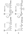
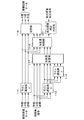
図1は、本実施例に係る表示装置の機能構成の一例を示す図である。
本実施例に係る表示装置は、液晶パネル部101、バックライト部102、特徴量検出部103、発光輝度決定部104、増加率決定部105、増加部106、補正部107、
などを有する。
<Example 1>
Hereinafter, a display device and a control method thereof according to
FIG. 1 is a diagram illustrating an example of a functional configuration of the display device according to the present embodiment.
The display device according to the present embodiment includes a liquid
Etc.
液晶パネル部101は、液晶パネル部101に入力された画像データに基づく画像を表示する表示部である。本実施例では、液晶パネル部101は、複数の液晶素子を有する透過型の表示部である。液晶パネル部101は、液晶パネル部101に入力された画像データに基づいて各液晶素子の透過率を制御する。そして、液晶パネル部101は、液晶パネル部101に入力された画像データに基づく透過率で、バックライト部102からの光を透過することにより画像を表示する。具体的には、液晶パネル部101は、液晶ドライバ、コントロール基板、液晶パネル、などを有する。液晶パネルは、複数の液晶素子を有する透過型液晶パネルである。コントロール基板は、画像データに応じた制御信号を液晶ドライバに出力する。液晶ドライバは、制御信号に応じて液晶パネルの透過率(各液晶素子の透過率)を制御する。そして、液晶パネル部101に入力された画像データに基づく透過率で、バックライト部102からの光が液晶パネルを透過することにより画像が表示される。
The liquid
バックライト部102は、液晶パネル部101の背面に対して光を発する発光部である。バックライト部102は、例えば、光源、光源を制御する制御回路、光源からの光を拡散させる光学ユニット、などを有する。制御回路によって光源の発光輝度が制御され、光源から発せられた光が光学ユニットで拡散されて液晶パネル部101の背面に照射される。本実施例では、バックライト部102は、画面の領域を構成する複数のバックライト領域のそれぞれについて発光輝度を制御可能な構成を有する。例えば、バックライト部102は、バックライト領域毎に、個別に制御可能な光源を有する。バックライト部102は、バックライト領域毎に、発光輝度制御値に応じた発光輝度で発光する。本実施例では、画面が水平方向m個(mは1以上の整数)、垂直方向n個(nは1以上の整数)の合計m×n個のバックライト領域に分割されているものとする。具体的には、本実施例では、m=4でありn=5であるものとする。また、本実施例では、発光輝度制御値が大きいほど発光輝度が高いものとする。
The
本実施例では、暗い画像が表示されるバックライト領域の発光輝度として、所定の発光輝度よりも低い値を設定する。そして、発光輝度の低下に応じた増加率で画像データの画素値を高めることにより、液晶パネル部101の透過率を高める。これにより、画面上の輝度を大きく低下させることなく、暗い画像が表示される領域において、バックライト部102からの光の漏れに起因する黒浮を低減することができる。
なお、本実施例では、説明を分かりやすくするため、入力される画像データの画素値の範囲と、液晶パネル部101の透過率を制御する画像データの画素値の範囲とが同一であるものとする。例えば、入力される画像データの画素値の範囲が0〜255であり、画素値が0のとき液晶パネル部101の透過率は最小になり、画素値が255のとき液晶パネル部101の透過率は最大になるものとする。以後、特に断りのない限り、画素値の取り得る範囲の最大値をDMAXとする。
In the present embodiment, a value lower than a predetermined light emission luminance is set as the light emission luminance of the backlight area where a dark image is displayed. And the transmittance | permeability of the liquid
In this embodiment, for easy understanding, the pixel value range of the input image data and the pixel value range of the image data for controlling the transmittance of the liquid
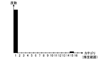
特徴量検出部103は、表示装置に入力された画像データ(入力画像データ)の特徴量を取得する。本実施例では、特徴量検出部103は、画面を分割して得られる画像領域毎に、その画像領域に表示される画像の特徴量を取得する。画像領域とバックライト領域は、1:1に対応していることが望ましい。本実施例では、特徴量として、画像領域に表示される画像の輝度ヒストグラムを取得する場合について説明する。このヒストグラムは、例えば、輝度の取り得る範囲(本実施例では0〜255の範囲)を32等分した32カテゴリのヒストグラムである。
なお、特徴量は、画像を解析することにより検出されてもよいし、外部から入力されてもよい。
The feature
Note that the feature amount may be detected by analyzing the image, or may be input from the outside.
発光輝度決定部104は、バックライト部102を発光させる。具体的には、発光輝度決定部104は、特徴量検出部103で取得された特徴量に基づく発光輝度でバックライト部102を発光させる。本実施例では、発光輝度決定部104は、特徴量検出部103で検出した画像領域毎の特徴量に基づいて、バックライト領域毎の発光輝度制御値を決定する。本実施例では、所定の発光輝度(標準発光輝度)に対応する発光輝度制御値(標準発光輝度制御値)を、画像領域毎の特徴量に基づく低下率で低下させることにより、発光輝度制御値を決定する。標準発光輝度は、例えば、バックライト領域毎の発光輝度の制御を行わない場合の発光輝度(バックライト全体を均一に発光させる場合の発光輝度)である。
なお、全ての画素について画素値に対応する輝度を実現するためには、少なくとも、最大の画素値に対応する輝度を実現可能な発光輝度でバックライト部102を発光させなければならない。しかし、発光輝度決定部104では、最大の画素値に対応する輝度が実現可能か否かを考慮せず、黒浮が抑制されるように、発光輝度が決定される。
The light emission
Note that, in order to realize the luminance corresponding to the pixel value for all the pixels, it is necessary to cause the
バックライト領域毎の発光輝度(発光輝度制御値)の決定方法について説明する。ここでは、画像領域とバックライト領域が1:1に対応しているものとする。
まず、発光輝度決定部104は、バックライト領域毎に、画像領域のヒストグラムを、画素値の大きいカテゴリからの累積ヒストグラムに変換する。
次に、発光輝度決定部104は、バックライト領域毎に、累積ヒストグラムにおいて、度数が閾値以上(例えば、総度数の1%以上)となるカテゴリ(画素値の範囲)の最大画素値HistHを検出する。
そして、発光輝度決定部104は、バックライト領域毎に、HistHをDMAXで除算した値を低下率として算出する。
次に、発光輝度決定部104は、バックライト領域毎に、標準発光輝度制御値に低下率を乗算することにより、発光輝度制御値を算出する。
図2に、ヒストグラムと累積ヒストグラムの一例を示す。図2(a)の例では、高い画素値のカテゴリ(画素値が239以下のカテゴリ)で度数が閾値以上となっているため、低下率は1に近い値となり、発光輝度制御値として、標準発光輝度制御値に近い値が得られる。図2(b)の例では、低い画素値のカテゴリ(画素値が127以下のカテゴリ)まで度数が閾値以上とならないため、低下率は小さな値となり、発光輝度制御値として、標準発光輝度制御値よりも大分低い値が得られる。
なお、本実施例では、輝度ヒストグラムに基づいて発光輝度(発光輝度制御値)を算出する構成としたが、発光輝度の決定方法はこれに限らない。例えば、演算を行わずに、特徴量と発光輝度制御値との対応関係を表すテーブルを用いて発光輝度制御値が決定されてもよい。画素値(RGB値など)のヒストグラムを用いて発光輝度制御値が決定されてもよい。画素値や輝度の平均値、分散、最大値、最小値、最頻値、中間値など、ヒストグラム以外の特徴量から発光輝度が決定されてもよい。特徴量として、複数種類の値(例えば、最大輝度と平均輝度)が用いられてもよい。
A method for determining the light emission luminance (light emission luminance control value) for each backlight region will be described. Here, it is assumed that the image area and the backlight area correspond to 1: 1.
First, the light emission
Next, the light emission
Then, the light emission
Next, the light emission
FIG. 2 shows an example of a histogram and a cumulative histogram. In the example of FIG. 2A, since the frequency is equal to or higher than the threshold in the category of high pixel values (category where the pixel value is 239 or less), the reduction rate is a value close to 1, and the light emission luminance control value is a standard value. A value close to the emission luminance control value is obtained. In the example of FIG. 2B, since the frequency does not exceed the threshold value until the category of the low pixel value (category where the pixel value is 127 or less), the decrease rate becomes a small value, and the standard emission luminance control value is used as the emission luminance control value. Much lower values are obtained.
In this embodiment, the light emission luminance (light emission luminance control value) is calculated based on the luminance histogram. However, the method for determining the light emission luminance is not limited to this. For example, the light emission luminance control value may be determined using a table representing the correspondence relationship between the feature amount and the light emission luminance control value without performing the calculation. The light emission luminance control value may be determined using a histogram of pixel values (RGB values, etc.). The light emission luminance may be determined from a feature amount other than the histogram, such as an average value of pixel values and luminance, variance, maximum value, minimum value, mode value, and intermediate value. A plurality of types of values (for example, maximum luminance and average luminance) may be used as the feature amount.
増加率決定部105と増加部106により、入力画像データに所定の画像処理が施される。それにより、処理画像データが生成される。本実施例では、所定の画像処理として、バックライト部102の発光輝度(発光輝度決定部104で決定された発光輝度制御値)にあわせて入力画像データを補正する処理が行われる。そして、所定の画像処理により、バックライト部102を標準発光輝度制御値で発光させた場合と、発光輝度決定部104で決定された発光輝度制御値で発光させた場合とで、画面上に表示される画像の輝度が等しくなるように、入力画像データが補正される。
The increase
増加率決定部105は、画素毎(または画像領域毎)に、発光輝度決定部104で決定された発光輝度の低下率に基づいて、画素値の増加率を決定する。例えば、バックライト部102を標準発光輝度制御値で発光させた場合と、発光輝度決定部104で決定された
発光輝度制御値で発光させた場合とで、画面上に表示される画像の輝度を一致させるためには、低下率の逆数を増加率とすればよい。
The increase
増加部106は、画素毎に、入力画像データの画素値を、増加率決定部105で決定された増加率で高めることにより、処理画像データを生成する。増加部106は、処理画像データを補正部107に出力する。
ここで、処理画像データの画素値が、所定の範囲外(液晶パネル部101に入力可能な画素値の範囲外)の値となることがある。具体的には、画素値を高めることにより、画素値がDMAX(液晶パネル部101に入力可能な画素値の最大値)を超えることがある。例えば、DMAX=255、入力画像データの画素値が200、増加率が1.5倍である場合には、処理画像データの画素値は300となり、DMAXを超える。以後、画素値のうち、DMAXを超えた分の値を飽和量とする。上記例では、飽和量は45である。
液晶パネル部101の透過率は、画素値がDMAXのときに最大となり、それ以上にすることはできない。そのため、画素値がDMAXを超える場合、画面上の輝度は、画素値に対応する輝度よりも低い値となってしまう(輝度の不足が生じる)。本実施例では、説明を簡単にするために、画素値の変化に対し、画面上の輝度が線形に変化するものとする。そのため、飽和量と、バックライト部102の発光輝度との積に比例する量の輝度が不足することになる。
The
Here, the pixel value of the processed image data may be a value outside a predetermined range (outside the range of pixel values that can be input to the liquid crystal panel unit 101). Specifically, by increasing the pixel value, the pixel value may exceed DMAX (the maximum pixel value that can be input to the liquid crystal panel unit 101). For example, when DMAX = 255, the pixel value of the input image data is 200, and the increase rate is 1.5 times, the pixel value of the processed image data is 300, which exceeds DMAX. Thereafter, the pixel value that exceeds DMAX is defined as the saturation amount. In the above example, the saturation amount is 45.
The transmittance of the liquid
補正部107は、処理画像データの画素値のうち所定の範囲外の画素値(DMAXより大きい画素値)を、所定の範囲内の値に制限することにより、制限画像データを生成する。本実施例では、補正部107は、制限前の画素値によって表される色相が保たれるように、画素値を制限することにより、制限画像データを生成する。本実施例では、画素値は、RGBの3つの色信号(R値、G値、B値)からなる。補正部107は、R値、G値、B値の比率(色バランス)が保たれるように、画素値を制限する。ここで、制限画像データを生成する際に画素値が制限された画素を“制限画素”と呼ぶ。
補正部107は、画素値を制限したことによる制限画素の輝度の変化が補償(抑制)されるように、当該制限画素の周囲の画素の画素値を調整することにより、制限画像データから補償画像データ(抑制画像データ)を生成する。具体的には、画素値を制限することにより制限画素の画素値がDMAX以下に低減され、制限画素の輝度が低下する。そのため、補正部107は、そのような輝度の低下が補償されるように、制限画素の周囲の画素の画素値を高める。また、本実施例では、補正部107は、1つの制限画素の輝度の変化を補償するために周囲の画素に与える画素値の調整量によって表される色相が、当該制限画素の制限前の画素値によって表される色相と一致するように、調整量を決定する。
そして、補正部107は、補償画像データを液晶パネル部101に出力する。
The
The
Then, the
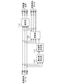
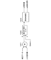
補正部107の機能構成の一例を図3に示す。
補正部107は、制限部108と補償部(抑制部)109を有する。
制限部108は、処理画像データの画素値のうち所定の範囲外の画素値(DMAXより大きい画素値)を、所定の範囲内の値に制限することにより、制限画像データを生成する。そして、各画素の制限量を表す制限量信号(処理画像データから制限画像データを減算した信号)と、制限画像データとを出力する。
補償部109は、制限部108により画素値が制限されたことによる制限画素の輝度の変化が補償(抑制)されるように、当該制限画素の周囲の画素の画素値を調整することにより、制限画像データから補償画像データ(抑制画像データ)を生成し、補償画像データを出力する。
An example of the functional configuration of the
The correcting
The
The
図4は、制限部108の機能構成の一例を示す。図5は、制限部108の処理の一例を示す。
制限部108は、最大値検出部110、制限率決定部111、除算部112、減算部1
13などを有する。
最大値検出部110は、画素毎に、処理画像データの画素値を構成するR値、G値、B値から、最大値を検出する。そして、最大値検出部110は、画素毎の最大値を出力する。
制限率決定部111は、画素毎に、DMAXに対する、最大値検出部110で検出された最大値の割合を、制限率として算出する。但し、DMAXに対する、最大値検出部110で検出された最大値の割合が1以下場合には、制限率は1とされる。そして、制限率決定部111は、画素毎の制限率を出力する。
例えば、R値、G値、B値が、それぞれ、220、384、128の場合には、384が最大値として検出される。そして、DMAX=255の場合には、制限率は、255を384で除算した値(約1.5)となる。
除算部112は、画素毎に、処理画像データの画素値を構成するR値、G値、B値を、制限率で除算することにより、制限画像データの画素値を算出する。そして、除算部112は、制限画像データ(各画素値が、処理画像データの画素値を制限率で除算して得られる値である画像データ)を出力する。
減算部113は、画素毎に、処理画像データの画素値から制限画像データの画素値を減算することにより、制限量信号の値(画素値)を算出する。そして、減算部113は、制限量信号(各画素値が、処理画像データの画素値から制限画像データの画素値を減算して得られる値である画像データ)を出力する。
FIG. 4 shows an example of a functional configuration of the
The limiting
13 and so on.
The maximum
The limit
For example, when the R value, G value, and B value are 220, 384, and 128, 384 is detected as the maximum value. When DMAX = 255, the limiting rate is a value obtained by dividing 255 by 384 (about 1.5).
The
The
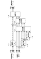
図6は、補償部109の機能構成の一例を示す。図7は、補償部109の処理の一例を示す。
補償部109は、ライン遅延部a114、ライン遅延部b115、ライン遅延部c116、加算量決定部117、加算量制限部118、加算部119などを有する。
FIG. 6 shows an example of a functional configuration of the
The
ライン遅延部a114、ライン遅延部b115、ライン遅延部c116は、それぞれ、入力された画像データを1ライン遅延させて出力する。
ライン遅延部a114には、制限画像データが入力される。そして、ライン遅延部a114からは、1ライン遅延した制限画像データが、1ライン遅延制限画像データとして出力される。
ライン遅延部b115には、制限量信号が入力される。そして、ライン遅延部b115からは、1ライン遅延した制限量信号が、1ライン遅延制限量信号として出力される。
ライン遅延部c116には、1ライン遅延制限量信号が入力される。そして、ライン遅延部c116からは、2ライン遅延した制限量信号が、2ライン遅延制限量信号として出力される。
The line delay unit a114, the line delay unit b115, and the line delay unit c116 each delay the input image data by one line and output it.
The limited image data is input to the line delay unit a114. The line delay unit a114 outputs the limited image data delayed by one line as the one-line delay limited image data.
A limit amount signal is input to the line delay unit b115. The line delay unit b115 outputs a limit amount signal delayed by one line as a one line delay limit amount signal.
A one-line delay limit amount signal is input to the line delay unit c116. Then, the limit amount signal delayed by two lines is output from the line delay unit c116 as a two-line delay limit amount signal.
加算量決定部117は、画素値の調整量を決定する。上述したように、本実施例では、1つの制限画素の輝度の変化を補償するために周囲の画素に与える画素値の調整量によって表される色相が、当該制限画素の制限前の画素値によって表される色相と一致するように、調整量が決定される。また、本実施例では、1つの制限画素の輝度の変化を複数の画素に補償させる際に、画素値の調整量が複数の画素間で互いに等しくなるように、複数の画素の画素値の調整量が決定される。
The addition
本実施例では、1つの注目画素の画素値を調整することにより、当該注目画素の上下左右に隣接する4つの画素の輝度の変化が補償される。
加算量決定部117は、画素毎に、その画素を調整対象の画素(注目画素)として、注目画素の上下左右に隣接する4つの画素(隣接画素)の輝度の変化を補償するための4つの調整量を決定する。本実施例では、1ライン遅延制限量信号の画素が注目画素とされる。また、1ライン遅延制限量信号の画素が注目画素の左右に隣接する画素とされる。そして、遅延されていない制限量信号の画素が注目画素の上に隣接する画素とされ、2ライン
遅延制限量信号の画素が注目画素の下に隣接する画素とされる。本実施例では、1つの制限画素の輝度の変化が4つの画素によって補償される。そのため、1つの制限画素の飽和量(制限量信号の値)の1/4が、当該制限画素の輝度の変化を補償するための注目画素の調整量とされる。
加算量決定部117は、注目画素に対し、上記4つの調整量の総和(総調整量)を、加算量として算出する。そして、加算量決定部117は、画素毎の加算量を出力する。
In the present embodiment, by adjusting the pixel value of one target pixel, the luminance change of four pixels adjacent to the target pixel in the vertical and horizontal directions is compensated.
For each pixel, the addition
The addition
加算量制限部118は、調整後の画素値が所定の範囲外の値となる画素が存在する場合に、当該画素の調整後の画素値が上記所定の範囲内の値となるように、当該画素の画素値の総調整量を制限する。具体的には、加算量制限部118は、1ライン遅延制限画像データの画素毎に、その画素の画素値に、加算量決定部117で決定された加算量を加算した後の画素値がDMAXより大きい値となるか否かを判断する。加算量制限部118は、加算量の加算後の画素値がDMAXより大きい値となる場合に、加算量の加算後の画素値がDMAX以下となるように、加算量を制限する(制限処理)。そして、加算量制限部118は、画素毎の制限処理後の加算量(制限加算量)を出力する。
When there is a pixel whose adjusted pixel value is outside the predetermined range, the addition
本実施例では、調整後の総調整量によって表される色相が、調整前の総調整量によって表される色相と一致するように、総調整量が制限される。具体的には、加算量制限部118は、加算量の利得Gを算出する。そして、加算量制限部118は、加算量を構成するR値、G値、B値に、利得Gを乗算することにより、制限加算量を算出する。
利得Gは、例えば、以下の方法で算出される。
まず、式1−1〜1−3を用いて、加算量を構成するR値の利得の最大値GMR、G値の利得の最大値GMG、B値の利得の最大値GMBが算出される。式1−1〜1−3において、DMAXは、液晶パネル部101に入力可能な画素値の最大値である。DR、DG、DBは、制限画像データの画素値を構成するR値、G値、B値である。OVR、OVG、OVBは、加算量を構成するR値、G値、B値である。
GMR=(DMAX−DR)/OVR ・・・(式1−1)
GMG=(DMAX−DG)/OVG ・・・(式1−2)
GMB=(DMAX−DB)/OVB ・・・(式1−3)
そして、利得GMR、利得GMG、利得GMBのうちの最小値が利得Gとして設定される。但し、利得GMR、利得GMG、利得GMBがいずれも1以上の場合には、1が利得Gとして設定される。
In the present embodiment, the total adjustment amount is limited so that the hue represented by the total adjustment amount after adjustment matches the hue represented by the total adjustment amount before adjustment. Specifically, the addition
The gain G is calculated by the following method, for example.
First, the maximum value GMR of the R value, the maximum value GMG of the G value, and the maximum value GMB of the B value that constitute the addition amount are calculated using the equations 1-1 to 1-3. In Expressions 1-1 to 1-3, DMAX is the maximum pixel value that can be input to the liquid
GMR = (DMAX-DR) / OVR (Formula 1-1)
GMG = (DMAX−DG) / OVG (Formula 1-2)
GMB = (DMAX-DB) / OVB (Formula 1-3)
Then, the minimum value among the gain GMR, gain GMG, and gain GMB is set as the gain G. However, when the gain GMR, the gain GMG, and the gain GMB are all 1 or more, 1 is set as the gain G.
加算部119は、1ライン遅延制限画像データの画素毎に、その画素の画素値に制限加算量を加算する。それにより、補償画像データが生成される。そして、加算部119は、生成した補償画像データを液晶パネル部101に出力する。
The adding
以上述べたように、本実施例によれば、画素値を制限したことによる制限画素の輝度の変化が補償されるように、当該制限画素の周囲の画素の画素値が調整される。それにより、所定の範囲外の画素値を当該所定の範囲内の値に制限することにより生じる画質の劣化を抑制することができる。具体的には、画素値を低減したことによる輝度の低下が、周囲の画素によって補われるため、視覚上の輝度の低下を抑制することができる。
また、本実施例によれば、輝度の変化を補償するために画素に与える調整量によって表される色相が、制限前の画素値の色相と一致するように処理が行われる。それにより、所定の範囲外の画素値を当該所定の範囲内の値に制限することにより生じる画質の劣化をより抑制することができる。具体的には、画素値を制限したことによる色の変化や、輝度を補償したことによる色の変化を抑制することができる。
また、本実施例によれば、調整後の画素値が所定の範囲外の値となる画素が存在する場
合に、当該画素の調整後の画素値が所定の範囲内の値となるように、当該画素の画素値の総調整量が制限される。具体的には、調整後の総調整量によって表される色相が、調整前の総調整量によって表される色相と一致するように、総調整量が制限される。それにより、所定の範囲外の画素値を当該所定の範囲内の値に制限することにより生じる画質の劣化をより抑制することができる。具体的には、調整後の画素値が所定の範囲外の値となる場合でも、輝度を補償したことによる色の変化を抑制することができる。
また、本実施例によれば、1つの制限画素の輝度の変化を複数の画素に補償させる際に、画素値の調整量が複数の画素間で互いに等しくなるように、複数の画素の画素値の調整量が決定される。それにより、補償による輝度むらの発生を抑制することができる。
As described above, according to the present embodiment, the pixel values of the pixels around the limited pixel are adjusted so that the change in the luminance of the limited pixel due to the limited pixel value is compensated. Thereby, it is possible to suppress deterioration in image quality caused by limiting pixel values outside the predetermined range to values within the predetermined range. Specifically, since the decrease in luminance due to the reduction in the pixel value is compensated by surrounding pixels, the decrease in visual luminance can be suppressed.
In addition, according to the present embodiment, the process is performed so that the hue represented by the adjustment amount given to the pixel to compensate for the change in luminance matches the hue of the pixel value before the restriction. Thereby, it is possible to further suppress deterioration in image quality caused by limiting pixel values outside the predetermined range to values within the predetermined range. Specifically, it is possible to suppress a color change caused by limiting the pixel value and a color change caused by compensating the luminance.
Further, according to this embodiment, when there is a pixel whose adjusted pixel value is outside the predetermined range, the adjusted pixel value of the pixel is set to a value within the predetermined range. The total adjustment amount of the pixel value of the pixel is limited. Specifically, the total adjustment amount is limited so that the hue represented by the total adjustment amount after adjustment matches the hue represented by the total adjustment amount before adjustment. Thereby, it is possible to further suppress deterioration in image quality caused by limiting pixel values outside the predetermined range to values within the predetermined range. Specifically, even when the adjusted pixel value is outside a predetermined range, a change in color due to luminance compensation can be suppressed.
In addition, according to the present embodiment, the pixel values of the plurality of pixels are set such that the adjustment amount of the pixel value is equal between the plurality of pixels when the luminance change of one limiting pixel is compensated for by the plurality of pixels. The amount of adjustment is determined. Thereby, the occurrence of uneven brightness due to compensation can be suppressed.
なお、本実施例では、画素値が上限値を超えた場合に、当該画素値を上限値に制限する例を示したが、これに限らない。制限後の画素値は、所定の範囲(画素値の取りうる範囲)内の値であればよく、上限値よりも小さい値であってもよい。
なお、本実施例では、画素値が所定の範囲(画素値の取りうる範囲)の上限値を超える場合について説明したが、これに限らない。画素値が所定の範囲の下限値を下回った場合には、当該画素値が下限値以上の値に制限されることがある。その場合には、同様の方法により、下限値を下回った画素値を制限したことによる輝度の変化が補償されてもよい。但し、下限値を下回った画素値を制限したことによる輝度の変化を補償すると、黒浮が生じる虞がある。そこで、黒浮の抑制を優先し、上限値を超えた画素値を制限したことによる輝度の変化のみが補償されてもよい。
なお、本実施例では、制限画素の上下左右に隣接する4つの画素が、制限画素の周囲の画素である場合の例を説明したが、制限画素の周囲の画素はこれに限らない。例えば、制限画素の上に隣接する2画素、下に隣接する2画素、左に隣接する2画素、右に隣接する2画素の計8画素が周囲の画素とされてもよい。制限画素の上、下、左、右、左上、右上、左下、右下に隣接する8画素が周囲の画素とされてもよい。
なお、本実施例では、画素値の増加に対して透過率(画面上の輝度)が線形に増加する場合の例を示したが、これに限らない。例えば、画素値の増加に対して透過率(画面上の輝度)が指数関数的に増加してもよい。その場合には、例えば、画素値に対する透過率の変化を表す関数を用いて、画素値を制限したことによる輝度の変化を算出(推定)することができる。そして、上記関数と、調整対象の画素の画素値(制限画像データの画素値)とから、輝度の変化を補償する補償量を算出することができる。
なお、注目画素が制限画素である場合には、加算量を加算する余地が少ない。そのため、そのような注目画素は、調整対象の画素として選択されなくてもよい。そして、本実施例では、1つの制限画素の輝度の変化を、当該制限画素の上下左右に隣接する4つの画素に補償させる構成としたが、1つの制限画素の輝度の変化が必ずしも上記4つの画素により補償されるとは限らない。例えば、上記4つの画素のうち、2つの画素の画素値がDMAXである場合には、制限画素の輝度の変化は残りの2つの画素でしか補償することができない。そのため、そのような場合には、制限画素の輝度の変化を1/2ずつ2つの画素で補償させることが好ましい。即ち、制限画素の周囲に存在する制限画素の数(制限画素以外の画素の数)に基づいて、補償量を決定することが好ましい。
なお、本実施例では、バックライト領域毎に発光輝度や画素値が調整される構成としたが、これに限らない。画像全体の明るさに基づいて、バックライト全体の発光輝度が制御され、バックライト全体の発光輝度に基づいて、各画素値が調整されてもよい。
なお、本実施例では、表示装置が液晶表示装置である場合の例を説明したが、表示装置は液晶表示装置に限らない。表示装置は、バックライト部と、バックライト部からの光を透過して画像を表示する表示部とを有する表示装置であればよい。
なお、1つの制限画素の輝度の変化を複数の画素に補償させる際に、画素値の調整量が複数の画素間で互いに異なっていてもよい。そのような場合であっても、上記効果に順じた効果を得ることができる。
なお、制限後の画素値の色相、輝度の変化を補償するために画素に与える調整量によっ
て表される色相は、制限前の画素値の色相と一致していなくてもよい。また、調整後の総調整量によって表される色相は、調整前の総調整量によって表される色相と一致していなくてもよい。そのような場合であっても、画素値を制限したことによる制限画素の輝度の変化が補償すれば、当該輝度の変化による画質の劣化を抑制することができる。
In the present embodiment, when the pixel value exceeds the upper limit value, the example is shown in which the pixel value is limited to the upper limit value. However, the present invention is not limited to this. The limited pixel value may be a value within a predetermined range (a range that the pixel value can take), and may be a value smaller than the upper limit value.
In the present embodiment, the case where the pixel value exceeds the upper limit value of the predetermined range (the range that the pixel value can take) has been described, but the present invention is not limited to this. When the pixel value falls below the lower limit value of the predetermined range, the pixel value may be limited to a value equal to or higher than the lower limit value. In that case, a change in luminance caused by limiting the pixel value below the lower limit value may be compensated by a similar method. However, if the change in luminance due to the limitation of the pixel value below the lower limit is compensated, there is a possibility that black floating may occur. Therefore, priority may be given to suppression of black floating, and only a change in luminance due to limiting pixel values exceeding the upper limit value may be compensated.
In the present embodiment, an example in which the four pixels adjacent to the restricted pixel in the vertical and horizontal directions are pixels around the restricted pixel is described. However, the pixels around the restricted pixel are not limited thereto. For example, a total of 8 pixels may be used as the surrounding pixels, that is, 2 pixels adjacent above the restricted pixel, 2 pixels adjacent below, 2 pixels adjacent to the left, and 2 pixels adjacent to the right. The eight pixels adjacent to the upper, lower, left, right, upper left, upper right, lower left, and lower right of the restricted pixels may be the surrounding pixels.
In the present embodiment, an example in which the transmittance (brightness on the screen) increases linearly with respect to an increase in pixel value is shown, but the present invention is not limited to this. For example, the transmittance (brightness on the screen) may increase exponentially as the pixel value increases. In that case, for example, a change in luminance caused by limiting the pixel value can be calculated (estimated) using a function representing a change in transmittance with respect to the pixel value. A compensation amount that compensates for a change in luminance can be calculated from the above function and the pixel value of the pixel to be adjusted (the pixel value of the restricted image data).
When the target pixel is a limited pixel, there is little room for adding the addition amount. Therefore, such a target pixel may not be selected as a pixel to be adjusted. In this embodiment, the luminance change of one limiting pixel is compensated for by four pixels adjacent to the limiting pixel in the vertical and horizontal directions. However, the luminance change of one limiting pixel is not necessarily the above four. It is not always compensated by the pixel. For example, when the pixel value of two of the four pixels is DMAX, the change in the luminance of the limited pixel can be compensated only for the remaining two pixels. Therefore, in such a case, it is preferable to compensate the change in luminance of the limited pixel by two pixels by 1/2. That is, it is preferable to determine the compensation amount based on the number of limited pixels existing around the limited pixel (the number of pixels other than the limited pixel).
In this embodiment, the light emission luminance and the pixel value are adjusted for each backlight region, but the present invention is not limited to this. The light emission luminance of the entire backlight may be controlled based on the brightness of the entire image, and each pixel value may be adjusted based on the light emission luminance of the entire backlight.
In this embodiment, an example in which the display device is a liquid crystal display device has been described. However, the display device is not limited to a liquid crystal display device. The display device may be a display device having a backlight unit and a display unit that transmits light from the backlight unit and displays an image.
Note that, when a plurality of pixels compensate for a change in luminance of one limited pixel, the adjustment amount of the pixel value may be different between the plurality of pixels. Even in such a case, an effect in accordance with the above effect can be obtained.
Note that the hue represented by the adjustment amount given to the pixel in order to compensate for the change in the hue and luminance of the pixel value after the restriction does not need to match the hue of the pixel value before the restriction. Further, the hue represented by the total adjustment amount after adjustment does not have to coincide with the hue represented by the total adjustment amount before adjustment. Even in such a case, if the change in the luminance of the restricted pixel due to the restriction of the pixel value is compensated, the deterioration of the image quality due to the luminance change can be suppressed.
<実施例2>
以下、本発明の実施例2に係る表示装置及びその制御方法について図面を参照して説明する。
実施例1では、全ての制限画素の飽和量を補償する構成について説明した。ここで、大面積の領域の画素値が制限されている場合には、注目画素の周囲に多くの制限画素が存在するため、注目画素の加算量が大きくなり、利得Gが小さくなる。そのため、大面積の領域の画素値が制限されている場合には、本発明の効果(画質の劣化を抑制する効果)が低下する。それだけでなく、大面積の領域の画素値が制限されている場合には、多くの制限画素の色が注目画素の色に加算されるため、画像のディテールが失われてしまう(画質が劣化してしまう)虞がある。制限画素は、制限画像データを生成する際に画素値が制限された画素であり、入力画像データに所定の画像処理を施すことにより画素値が所定の範囲外の値となる画素である。
一方、局所的に存在する制限画素(孤立制限画素)の輝度の変化を補償する場合には、利得Gは1に近い値となり、本発明の効果として高い効果を得ることができる。
そこで、本実施例では、処理画像データの画素値のうち、制限画素の画素値を所定範囲内の値に制限し、孤立制限画素の周囲の画素の画素値を、当該孤立制限画素の画素値を制限したことによる輝度の変化が補償されるように調整する。処理画像データは、入力画像データに所定の画像処理を施すことにより生成される画像データである。
本実施例では、高い効果を得ることのできる孤立制限画素に限定して、当該孤立制限画素の輝度の変化が補償されるため、高い効果を得ることができる。
<Example 2>
Hereinafter, a display device and a control method thereof according to
In the first embodiment, the configuration for compensating for the saturation amount of all the limited pixels has been described. Here, when the pixel value of the large area is limited, there are many limited pixels around the pixel of interest, so the amount of addition of the pixel of interest increases and the gain G decreases. Therefore, when the pixel value of the large area region is limited, the effect of the present invention (the effect of suppressing the deterioration of image quality) is reduced. In addition, when the pixel value of a large area is restricted, the color of many restricted pixels is added to the color of the pixel of interest, resulting in loss of image details (image quality deteriorates). There is a risk. The limited pixel is a pixel whose pixel value is limited when generating the limited image data, and is a pixel whose pixel value falls outside a predetermined range by performing predetermined image processing on the input image data.
On the other hand, when compensating for a change in luminance of a locally existing limited pixel (isolated limited pixel), the gain G becomes a value close to 1, and a high effect can be obtained as an effect of the present invention.
Therefore, in this embodiment, among the pixel values of the processed image data, the pixel value of the limited pixel is limited to a value within a predetermined range, and the pixel values of the pixels around the isolated limited pixel are set to the pixel value of the isolated limited pixel. Adjustment is made so as to compensate for a change in luminance due to the limitation. The processed image data is image data generated by performing predetermined image processing on the input image data.
In the present embodiment, since the change in the luminance of the isolated limited pixel is compensated only for the isolated limited pixel that can obtain a high effect, a high effect can be obtained.
図8は、実施例2に係る補償部の機能構成の一例を示す。
本実施例に係る補償部は、ライン遅延部a114、ライン遅延部b115、ライン遅延部c116、加算量決定部117、加算量制限部218、加算部119、加算量制御部220などを有する。
ライン遅延部a114、ライン遅延部b115、ライン遅延部c116、加算量決定部117、加算部119の動作は実施例1と同じである。
FIG. 8 illustrates an example of a functional configuration of the compensation unit according to the second embodiment.
The compensation unit according to the present embodiment includes a line delay unit a114, a line delay unit b115, a line delay unit c116, an addition
The operations of the line delay unit a114, the line delay unit b115, the line delay unit c116, the addition
加算量制御部220は、孤立制限画素以外の制限画素の輝度の変化が補償されないように、制限画素が孤立制限画素か否かを判定する。制限画素が孤立制限画素か否かは、制限画素の配置に基づいて判定することができる。
注目画素の周囲に存在する制限画素の数が所定数より多い場合には、当該制限画素が孤立制限画素である可能性が低い。そこで、本実施例では、加算量制御部220は、一の画素(注目画素)の周囲に存在する制限画素の数が所定数以下である場合に、当該制限画素が孤立制限画素であると判定する。具体的には、加算量制御部220は、注目画素の上下左右に隣接する4つの画素のうち、3つ以上の画素が制限画素である場合には、それら制限画素が孤立制限画素ではないと判定する。そして、加算量制御部220は、注目画素の上下左右に隣接する4つの画素のうち、2つ以下の画素が制限画素である場合には、それら制限画素が孤立制限画素であると判定する。加算量制御部220は、注目画素の周囲の制限画素が孤立制限画素である場合には、制御信号として0を出力し、注目画素の周囲の制限画素が孤立制限画素でない場合には、制御信号として1を出力する。
The addition
When the number of limit pixels existing around the pixel of interest is greater than a predetermined number, it is unlikely that the limit pixel is an isolated limit pixel. Therefore, in this embodiment, the addition
加算量制限部218は、実施例1で説明した加算量制限部118と同様に制限加算量を算出するが、制御信号が1の場合には、制限加算量を0に置き換える。このように、制限加算量を0に置き換えることにより、加算部119において、孤立制限画素の画素値を制
限したことによる輝度の変化が補償されるように、当該孤立制限画素の周囲の画素の画素値が調整される。
The addition
以上述べたように、本実施例によれば、孤立制限画素の画素値を制限したことによる輝度の変化が補償されるように、当該孤立制限画素の周囲の画素の画素値が調整される。それにより、画質の劣化を抑制する効果として高い効果を得ることができる。具体的には、意図しない画素の画素値が調整され、画質が劣化してしまうことを抑制することができる。
なお、孤立制限画素の検出方法は上記方法に限らない。例えば、制限画素のみからなる領域を検出し、その領域のサイズが所定値以下の場合に、当該領域が孤立制限画素からなる領域であると判定してもよい。また、制限画素に隣接する画素の中に、当該制限画素の画素値に比べ所定値以上低い画素値を有する画素が所定数(例えば2つ)以上存在する場合に、当該制限画素が孤立制限画素であると判定してもよい。
As described above, according to the present embodiment, the pixel values of the pixels around the isolated limited pixel are adjusted so that the change in luminance due to the limited pixel value of the isolated limited pixel is compensated. Thereby, a high effect can be obtained as an effect of suppressing the deterioration of the image quality. Specifically, the pixel value of an unintended pixel is adjusted, and deterioration of image quality can be suppressed.
Note that the detection method of the isolated limited pixel is not limited to the above method. For example, when an area including only limited pixels is detected and the size of the area is equal to or smaller than a predetermined value, it may be determined that the area is an area including isolated limited pixels. In addition, when there are a predetermined number (for example, two) or more of pixels having a pixel value lower than the pixel value of the restriction pixel by a predetermined value or more, the restriction pixel is an isolated restriction pixel. It may be determined that
<実施例3>
以下、本発明の実施例3に係る表示装置およびその制御方法について図面を参照して説明する。実施例1では、総調整量で画素値を調整することができない場合、具体的には加算量によって画素値がDMAXを超えてしまう場合に、利得Gによって加算量を制限する構成について説明した。注目画素の周囲の制限画素が孤立制限画素である場合には、利得Gは1に近い値となる可能性が高いが、注目画素の周囲の制限画素が孤立制限画素でない場合には、利得Gは1から離れた小さな値となる可能性が高い。利得Gが1に近い場合には、加算量(調整量)を制限したことによる輝度の変化が小さく、制限画素の輝度の変化が十分に補償されるため、本発明の効果(画質の劣化を抑制する効果)として高い効果が得られる。しかしながら、利得Gが1から離れた小さな値である場合には、加算量(調整量)を制限したことによる輝度の変化(低下)が大きく、制限画素の輝度の変化が十分に補償されない、本発明の効果として高い効果を得ることができない。
調整量を制限したことによる輝度の変化は、例えば、バックライト部の発光輝度を制御することにより補償することができる。
そこで、本実施例では、総調整量を制限したことによる輝度の変化が補償されるように、バックライト部の発光輝度を制御する。具体的には、バックライト領域毎(画像領域毎)に、その領域内の各画素の利得Gに基づいて、発光輝度決定部104で決定される低下率を補正する。それにより、利得Gが1から離れた小さな値である場合にも、画質の劣化を抑制する効果として高い効果を得ることを可能にする。
<Example 3>
Hereinafter, a display device and a control method thereof according to
The change in luminance due to the limitation of the adjustment amount can be compensated for, for example, by controlling the light emission luminance of the backlight unit.
Therefore, in this embodiment, the light emission luminance of the backlight unit is controlled so that the change in luminance due to the limitation of the total adjustment amount is compensated. Specifically, for each backlight region (each image region), the reduction rate determined by the light emission
図9は、本実施例に係る表示装置の機能構成の一例を示す図である。
本実施例に係る表示装置は、液晶パネル部101、バックライト部102、特徴量検出部103、発光輝度決定部304、増加率決定部105、増加部106、補正部307、などを有する。
液晶パネル部101、バックライト部102、特徴量検出部103、増加率決定部105、増加部106の動作は実施例1と同じである。
FIG. 9 is a diagram illustrating an example of a functional configuration of the display device according to the present embodiment.
The display device according to the present embodiment includes a liquid
The operations of the liquid
補正部307は、実施例1で説明した補正部107と同様に、補償画像データを生成し出力する。また、補正部307は、発光輝度を補正するための発光輝度補正信号を生成し出力する。
補正部307の機能構成の一例を図10に示す。
補正部307は、制限部108と補償部309を有する。
制限部108の動作は実施例1と同じである。
補償部309は、実施例1で説明した補償部109と同様に、補償画像データを生成し出力する。また、補償部309は、バックライト領域毎に、その領域内の各画素の利得Gを表す統計量情報に基づいて、その領域の発光輝度が不足しているか否か(制限画素の輝
度の変化が十分に補償されているか否か)を判定する。そして、補償部309は、その判定結果に基づいて、バックライト領域毎の発光輝度を補正するための発光輝度補正信号を生成し、出力する。
The
An example of the functional configuration of the
The
The operation of the limiting
The
補償部309の機能構成の一例を図11に示す。
補償部309は、ライン遅延部a114、ライン遅延部b115、ライン遅延部c116、加算量決定部117、加算量制限部318、加算部119、発光輝度補正判定部321などを有する。
ライン遅延部a114、ライン遅延部b115、ライン遅延部c116、加算量決定部117、加算部119の動作は実施例1と同じである。
An example of the functional configuration of the
The
The operations of the line delay unit a114, the line delay unit b115, the line delay unit c116, the addition
加算量制限部318の基本的な動作は、実施例1で説明した加算量制限部118と同じであるが、加算量制限部318は、各画素の利得Gを出力する処理をさらに行う。
The basic operation of the addition
発光輝度補正判定部321は、バックライト領域毎に、その領域内の各画素の利得Gの平均値(平均利得)を算出する。発光輝度補正判定部321は、バックライト領域毎に、平均利得が所定値より大きいか否かを判定する。そして、発光輝度補正判定部321は、平均利得が所定値より大きいバックライト領域に対して0が設定され、平均利得が所定値より小さいバックライト領域に対して1が設定された発光輝度補正信号を生成し、出力する。ここで、所定値とは、加算量(総調整量)の切り捨て、即ち画素値を制限したことによる輝度の変化をどの程度許容するかに基づいて決められる。例えば、5%の加算量(総調整量)の切り捨てを許容する場合には、所定値として0.95が使用される。
The light emission luminance
発光輝度決定部304は、加算量(総調整量)を制限したことによる輝度の変化が補償されるように、バックライト部102の発光輝度を制御する。本実施例では、発光輝度決定部304は、実施例1で説明した発光輝度決定部104と同様に、バックライト領域毎の低下率を算出する。発光輝度決定部304は、補償部309から出力される発光輝度補正信号に基づいてバックライト領域毎の低下率を補正する。
以下、発光輝度決定部304の処理について具体的に説明する。
まず、発光輝度決定部304は、フレーム毎に、各バックライト領域について、発光輝度補正信号の値に応じたカウント処理を行う。発光輝度補正信号の値が1のときには補正値を1カウントアップする。発光輝度補正信号の値が0のときには補正値を1カウントダウンする。補正値の初期値及び下限値は0とする。
そして、発光輝度決定部304は、バックライト領域毎に、補正値に所定の定数KTを乗算し、その値を低下率に加算する。定数KTが0.002の場合には、50フレームの期間で発光輝度補正信号の値が1のときに、低下率が0.1上昇する。このように、発光輝度補正信号として1が出力されているバックライト領域では、低下率が徐々に上昇し、発光輝度も徐々に上昇する。発光輝度が十分な値に達し、平均利得が閾値より大きくなると、発光輝度補正信号として0が出力されるようになり、発光輝度は一定とされる。
なお、低下率ではなく発光輝度制御値が補正されてもよい。
The light emission
Hereinafter, the process of the light emission
First, the light emission
Then, the light emission
Note that the light emission luminance control value may be corrected instead of the decrease rate.
以上述べたように、本実施例によれば、総調整量を制限したことによる輝度の変化が補償されるように、バックライト部の発光輝度が制御される。それにより、画質の劣化を抑制する効果として高い効果を得ることができる。具体的には、画素値を制限したことによる輝度の変化が十分に補償できない場合に、バックライトの発光輝度を制御することにより、当該輝度の変化を十分に補償することが可能となる。
なお、本実施例の構成(総調整量を制限したことによる輝度の変化が補償されるように、バックライト部の発光輝度を制御する構成)は、実施例2の構成に適用することもできる。
As described above, according to the present embodiment, the light emission luminance of the backlight unit is controlled so as to compensate for the luminance change caused by limiting the total adjustment amount. Thereby, a high effect can be obtained as an effect of suppressing the deterioration of the image quality. Specifically, when the change in luminance due to the limited pixel value cannot be sufficiently compensated, the change in luminance can be sufficiently compensated by controlling the light emission luminance of the backlight.
Note that the configuration of the present embodiment (the configuration in which the light emission luminance of the backlight unit is controlled so as to compensate for the change in luminance caused by limiting the total adjustment amount) can also be applied to the configuration of the second embodiment. .
<実施例4>
以下、本発明の実施例4に係る表示装置およびその制御方法について図面を参照して説明する。本実施例では、実施例3とは異なる方法により、画素値を制限したことによる輝度の変化が十分に補償できない場合にも、当該輝度の変化を十分に補償することを可能とする構成について説明する。なお、本実施例の構成は、実施例3の構成に適用することもできる。
<Example 4>
Hereinafter, a display device and a control method thereof according to
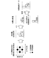
図12は、本実施例に係る補償部の機能構成の一例を示す図である。
本実施例に係る補償部は、総調整量が制限された画素である総調整量制限画素の総調整量を制限したことによる輝度の変化が補償されるように、当該総調整量制限画素の周囲の画素の画素値を調整する。
補償部は、第1制限画素検出部422、第1分配係数決定部423、第1加算量決定部424、第1加算量制限部425、第1加算部426、第2制限画素検出部427、第2分配係数決定部428、第2加算量決定部429、第2加算量制限部430、第2加算部431などを有する。なお、実施例1で説明したライン遅延部は省略している。
FIG. 12 is a diagram illustrating an example of a functional configuration of the compensation unit according to the present embodiment.
The compensation unit according to the present embodiment is configured so that the change in luminance due to the restriction of the total adjustment amount of the total adjustment amount restriction pixel that is a pixel in which the total adjustment amount is restricted is compensated for. Adjust the pixel values of surrounding pixels.
The compensation unit includes a first limit
実施例1では、制限画素の輝度の変化を上下左右に隣接する4画素で補償した。本実施例では、制限画素の輝度の変化を、制限画素の上、下、左、右、左上、右上、左下、右下に隣接する8画素で補償する。即ち、図13に示すように、1つの注目画素により、注目画素の上、下、左、右、左上、右上、左下、右下に隣接する8画素(8つの隣接画素)の輝度の変化が補償される。 In the first embodiment, the change in luminance of the limited pixel is compensated for by four pixels adjacent vertically and horizontally. In the present embodiment, the change in the luminance of the limited pixel is compensated by 8 pixels adjacent to the limited pixel above, below, left, right, upper left, upper right, lower left, and lower right. That is, as shown in FIG. 13, a change in luminance of eight pixels (eight adjacent pixels) adjacent to the upper, lower, left, right, upper left, upper right, lower left, and lower right of the target pixel is caused by one target pixel. Compensated.
図13のaは、表示装置に入力された入力画像データの一例を示す。なお、図13では、画素値の変化(画素値の調整方法)を分かりやすくするために、R値、G値、B値の3つの値のうちの1つに着目し、残りの2つの値は着目した値よりも小さいものとする。
ここで、増加率が3であり、DMAXが255であったとすると、符号bで示す制限画像データと、符号cで示す制限量信号(第1制限量信号)とが得られる。
第1制限画素検出部422は、第1制限量信号に基づいて、制限画素を検出し、検出結果を第1制限画素データとして出力する。具体的には、第1制限画素検出部422は、第1制限量信号の値が0でない画素を制限画素として検出する。そして、第1制限画素検出部422は、制限画素に1が割り当てられ、それ以外の画素に0が割り当てられた第1制限画素データを生成し、出力する。符号cで示す第1制限量信号から、符号dで示す第1制限画素データが得られる。
FIG. 13A shows an example of input image data input to the display device. In FIG. 13, in order to make it easy to understand the change in the pixel value (the adjustment method of the pixel value), attention is paid to one of the three values of the R value, the G value, and the B value, and the remaining two values. Is smaller than the focused value.
Here, if the increase rate is 3 and DMAX is 255, the limited image data indicated by the symbol b and the limit amount signal (first limit amount signal) indicated by the symbol c are obtained.
The first limit
第1分配係数決定部423は、第1制限画素データに基づいて第1分配係数を算出する。分配係数は、周囲の画素に分配する飽和量の割合を表す。例えば、画素の分配係数が1/5の場合には、その画素の飽和量の1/5が周囲の画素に分配される。即ち、分配係数が1/5の制限画素の飽和量が補償されるように注目画素の画素値を調整する場合には、当該制限画素の飽和量の1/5が注目画素の画素値の調整量となる。第1分配係数決定部423は、画素毎に、その画素の周囲の画素(8つの隣接画素)のうち、制限画素以外の画素(第1制限画素データの値が0の画素)の数の逆数を第1分配係数として設定する。但し、制限画素以外の画素の数が0の場合(8つの隣接画素の全てが制限画素である場合)には、制限画素以外の画素が存在しないことを表す値(0など)を設定する。そして、第1分配係数決定部423は、画素毎の第1分配係数を表す第1分配係数データを出力する。符号dで示す第1制限画素データから、符号eで示す第1分配係数データが得られる。
The first distribution
第1加算量決定部424は、第1制限量信号と第1分配係数データとに基づいて、各画素の加算量(第1加算量)を算出する。具体的には、画素毎に、その周囲の画素(8つの隣接画素)の飽和量を、第1分配係数に応じた重みで重み付け加算することにより、第1
加算量が算出される。また、本実施例では、制限画素に対しては、輝度の変化を補償するための画素値の調整を行わないため、第1加算量は0とされる。第1加算量決定部424は、画素毎に第1加算量を表す第1加算量データを出力する。符号cで示す第1制限量信号と、符号eで示す第1分配係数データとから、符号fで示す第1加算量データが得られる。
The first addition
The amount of addition is calculated. In the present embodiment, the first addition amount is set to 0 for the limited pixel because the pixel value is not adjusted to compensate for the change in luminance. The first addition
第1加算量制限部425は、実施例1で説明した加算量制限部118と同様に、第1加算量を制限画像データの画素値に加算した際に画素値がDMAXを超えないように、第1加算量を制限する(制限処理)。そして、第1加算量制限部425は、制限処理後の第1加算量データを、第1制限加算量データとして出力する。また、第1加算量制限部425は、画素毎に上記制限処理による制限量を表す第2制限量信号を出力する。符号bで示す制限画像データと、符号fで示す第1加算量データとから、符号gで示す第2制限量信号が得られる。
Similar to the addition
第1加算部426は、実施例1で説明した加算部119と同様に、第1制限加算量データと制限画像データから、補償画像データ(第1補償画像データ)を生成し、出力する。図13の例では、符号hで示す第1補償画像データが得られる。
Similar to the adding
第2制限画素検出部427は、第1制限画素検出部422と同様に、第2制限量信号に基づいて制限画素を検出する。ここでの“制限画素”は、総調整量が制限された画素である総調整量制限画素である。第2制限画素検出部427は、総調整量制限画素と、第1制限画素検出部422で検出された制限画素とに、1が割り当てられ、それ以外の画素に0が割り当てられた第2制限画素データを生成し、出力する。即ち、第2制限画素検出部427は、第1制限画素検出部422で検出された制限画素に加算量が加算されないように、総調整量制限画素の検出結果と、第1制限画素検出部422の検出結果との論理和を第2制限画素データとして出力する。符号gで示す第2制限量信号と、符号dで示す第1制限画素データとから、符号iで示す第2制限画素データが得られる。
Similar to the first limit
第2分配係数決定部428は、第1分配係数決定部423と同様に、第2制限画素データに基づいて分配係数(第2分配係数)を算出する。そして、第2分配係数決定部428は、画素毎の第2分配係数を表す第2分配係数データを出力する。符号iで示す第2制限画素データから、符号jで示す第2分配係数データが得られる。
Similar to the first distribution
第2加算量決定部429は、第1加算量決定部424と同様に、第2制限量信号と第2分配係数データとに基づいて、各画素の加算量(第2加算量)を算出する。そして、第2加算量決定部429は、画素毎に第2加算量を表す第2加算量データを出力する。符号iで示す第2制限量信号と、符号jで示す第2分配係数データとから、符号kで示す第2加算量データが得られる。
Similar to the first addition
第2加算量制限部430は、第1加算量制限部425と同様に、第2加算量を第1補償画像データの画素値に加算した際に画素値がDMAXを超えないように、第2加算量を制限する(制限処理)。そして、第2加算量制限部430は、制限処理後の第2加算量データを、第2制限加算量データとして出力する。なお、ここでは、制限処理による制限量を表す信号(データ)の出力は行われない。符号hで示す第1補償画像データに、符号kで示す第2加算量データを加算しても、画素値はDMAXを超えないため、第2制限加算量データは、符号kで示す第2加算量データと同じとなる。
Similarly to the first addition
第2加算部431は、第1加算部426と同様に、第2制限加算量データと第1補償画像データから、補償画像データ(第2補償画像データ;最終的な補償画像データ)を生成し、出力する。図13の例では、符号hで示す第1補償画像データと、符号kで示す第2
加算量データ(第2制限加算量データ)とから、符号lで示す第2補償画像データが得られる。
Similar to the
From the added amount data (second limited added amount data), second compensated image data indicated by
すなわち、第2制限画素検出部427、第2分配係数決定部428、第2加算量決定部429、第2加算量制限部430、及び第2加算部431により、第1制限画素検出部422、第1分配係数決定部423、第1加算量決定部424、第1加算量制限部425、及び第1加算部426による処理(補償処理)が繰り返される。
That is, the second limited
以上述べたように、本実施例によれば、総調整量制限画素の総調整量を制限したことによる輝度の変化が補償されるように、当該総調整量制限画素の周囲の画素の画素値が調整される。それにより、画質の劣化を抑制する効果として高い効果を得ることができる。具体的には、画素値を制限したことによる輝度の変化が十分に補償できない場合に、総調整量制限画素の周囲の画素の画素値を調整することにより、当該輝度の変化を十分に補償することが可能となる。
なお、本実施例では、補償処理を2回繰り返す構成としたが、補償処理の繰り返し回数を増やせば、画素値を制限したことによる輝度の変化をより確実に補償することができる。
なお、本実施例の構成(総調整量制限画素の周囲の画素の画素値を調整する構成)は、実施例2や実施例3の構成に適用することもできる。
As described above, according to this embodiment, the pixel values of the pixels around the total adjustment amount limiting pixel are compensated so that the change in luminance caused by limiting the total adjustment amount of the total adjustment amount limiting pixel is compensated. Is adjusted. Thereby, a high effect can be obtained as an effect of suppressing the deterioration of the image quality. Specifically, when the change in luminance due to the restriction of the pixel value cannot be sufficiently compensated, the change in the luminance is sufficiently compensated by adjusting the pixel values of the pixels around the total adjustment amount restriction pixel. It becomes possible.
In this embodiment, the compensation process is repeated twice. However, if the number of times the compensation process is repeated is increased, a change in luminance due to the limitation of the pixel value can be more reliably compensated.
Note that the configuration of the present embodiment (the configuration of adjusting the pixel values of the pixels around the total adjustment amount limiting pixel) can also be applied to the configurations of the second and third embodiments.
<実施例5>
以下、本発明の実施例5に係る表示装置およびその制御方法について図面を参照して説明する。実施例1〜4では、バックライトの発光輝度にあわせて入力画像データを補正する画像処理により、画素値が所定の範囲外の値となってしまう場合の例を説明した。しかし、上記画像処理以外の画像処理によっても、画素値が所定の範囲外の値となり、画素値が所定の範囲内の値に制限されてしまうことがある。画像処理の種類に依らず、画素値が所定の範囲内の値に制限されれば、画素値を制限したことによる輝度の変化が生じ、画質が劣化してしまう。そこで、本実施例では、上記画像処理とは異なる画像処理を行う表示装置の例を説明する。
<Example 5>
Hereinafter, a display device and a control method thereof according to
図14は、本実施例に係る表示装置の機能構成の一例を示す図である。
本実施例に係る表示装置は、表示部501、画像処理部532、制限部108、補償部109などを有する。
制限部108と補償部109の動作は実施例1と同じである。
表示部501は、画像データに基づく画像を表示する表示パネルである。表示部501は、例えば、有機ELディスプレイパネルやプラズマディスプレイパネルなどである。
FIG. 14 is a diagram illustrating an example of a functional configuration of the display device according to the present embodiment.
The display device according to the present embodiment includes a
The operations of the limiting
The
画像処理部532は、例えば、処理後の画素値が所定の範囲外の値となる可能性のある所定の画像処理を入力画像データに施すことにより、処理画像データを生成する。そして、画像処理部532は、生成した処理画像データを出力する。所定の画像処理は、エッジ強調処理、ぼかし処理、色調整処理、輝度調整処理、階調変換処理などである。処理後の画素値が所定の範囲外の値となると、実施例1で述べたように、輝度や色が所望の値と異なる値となってしまう。
For example, the
本実施例では、実施例1と同様に、画像処理部532の画像処理により所定の範囲外の値となった画素値が、制限部108により所定の範囲内の値に制限される。そして、実施例1と同様に、制限画素の画素値が制限されたことによる輝度の変化が補償されるように、当該制限画素の周囲の画素値が調整される。それにより、実施例1と同様に、所定の範囲外の画素値を当該所定の範囲内の値に制限することにより生じる画質の劣化を抑制することができる。
In the present embodiment, similarly to the first embodiment, the pixel value that is outside the predetermined range by the image processing of the
図15に、本実施例に係る表示装置の処理の一例(各種信号値の一例)を示す。
図15の例では、画像処理によりG値がDMAXを超える。そのため、色バランスを保ちながら、G値がDMAXとなるように、R値、G値、B値が調整(制限)されることにより、制限画像データが生成される。そして、当該調整による画素値の変化分(制限量)が、色バランスを保ちながら、周囲の画素の画素値に加算され、補償画像データが生成される。
FIG. 15 shows an example of processing (an example of various signal values) of the display device according to the present embodiment.
In the example of FIG. 15, the G value exceeds DMAX by image processing. Therefore, the restricted image data is generated by adjusting (restricting) the R value, the G value, and the B value so that the G value becomes DMAX while maintaining the color balance. Then, the change amount (limit amount) of the pixel value due to the adjustment is added to the pixel values of the surrounding pixels while maintaining the color balance, and compensated image data is generated.
以上述べたように、本実施例によれば、バックライトの発光輝度にあわせて入力画像データを補正する画像処理以外の画像処理により、画素値が所定の範囲外の値となる場合でも、画素値を制限することにより生じる画質の劣化を抑制することができる。
なお、本実施例の構成(バックライトの発光輝度にあわせて入力画像データを補正する画像処理以外の画像処理が行われる構成)は、実施例2〜4の構成に適用することもできる。
なお、本実施例に係る表示装置は、実施例1〜4のような表示装置(バックライト部と、バックライト部からの光を透過して画像を表示する表示装置)に限らない。本実施例に係る表示装置は、独立した光源を有さない表示装置であってもよい。
As described above, according to this embodiment, even when the pixel value is outside the predetermined range due to image processing other than the image processing for correcting the input image data in accordance with the light emission luminance of the backlight, It is possible to suppress deterioration in image quality caused by limiting the value.
Note that the configuration of this embodiment (a configuration in which image processing other than image processing for correcting input image data in accordance with the light emission luminance of the backlight is performed) can also be applied to the configurations of
Note that the display device according to the present embodiment is not limited to the display devices (the backlight unit and the display device that transmits light from the backlight unit and displays an image) as in the first to fourth embodiments. The display device according to the present embodiment may be a display device that does not have an independent light source.
<実施例6>
以下、本発明の本発明の実施例6に係る表示装置及びその制御方法について図面を参照して説明する。
実施例1〜5では、入力画像データに所定の画像処理を施すことにより処理画像データを生成し、処理画像データの画素値を調整する例を説明した。本実施例では、処理画像データを生成しない例を説明する。
図16は、本実施例に係る表示装置の機能構成の一例を示すブロック図である。本実施例に係る表示装置は、液晶パネル部101、バックライト部102、特徴量検出部103、発光輝度決定部104、補正データ生成部1605、制限画素検出部1606、補正データ調整部1607、補正部1608、Limit部1609、などを有する。
<Example 6>
Hereinafter, a display device and a control method thereof according to
In the first to fifth embodiments, an example has been described in which processed image data is generated by performing predetermined image processing on input image data, and pixel values of the processed image data are adjusted. In the present embodiment, an example in which processed image data is not generated will be described.
FIG. 16 is a block diagram illustrating an example of a functional configuration of the display device according to the present embodiment. The display device according to this embodiment includes a liquid
液晶パネル部101、バックライト部102、特徴量検出部103の動作は、実施例1と同じである。
図28に入力画像データの一例を示す。図28に示す入力画像データのうち、ひときわ明るい星(P部)を含む画像領域に対しては、特徴量として、図17に示すようなヒストグラムが得られる。図17は、輝度の取り得る範囲(本実施例では0〜255)を16等分した16カテゴリのヒストグラムの例である。図17のヒストグラムでは、0〜15の輝度範囲であるカテゴリ1に度数が集中している。また、図17の例では、224〜239の輝度範囲であるカテゴリ15の画素も少しだけ存在している。図17において、カテゴリ15の画素は、P部の画素である。
The operations of the liquid
FIG. 28 shows an example of input image data. In the input image data shown in FIG. 28, a histogram as shown in FIG. 17 is obtained as a feature amount for an image area including a particularly bright star (P portion). FIG. 17 is an example of a 16-category histogram in which the range of brightness that can be taken (0 to 255 in this embodiment) is divided into 16 equal parts. In the histogram of FIG. 17, the frequencies are concentrated in
発光輝度決定部104は、実施例1と同様の機能を有する。但し、本実施例では、実施例1とは異なる方法で発光輝度が決定されるものとする。
具体的には、発光輝度決定部104は、バックライト領域毎に、そのバックライト領域に対応する画像領域のヒストグラムから、最大カテゴリを判断する。最大カテゴリは、度数が1以上のカテゴリのうち、最も高輝度側のカテゴリである。そして、発光輝度決定部104は、最大カテゴリの番号が大きいほど発光輝度が高くなるように(バックライト領域に表示される画像の最大輝度が高いほど発光輝度が高くなるように)、バックライト領域毎に発光輝度を決定する。なお、本実施例では、16個のカテゴリに対して、低階調側から順番に1〜16の番号が付されているものとする。
しかしながら、図17に示すようなヒストグラムが得られるバックライト領域に表示される画像は、明るい領域を少ししか含まず、暗い領域を多く含む。そして、そのようなバ
ックライト領域の発光輝度を、最大カテゴリの番号に応じた高い値に制御してしまうと、図28に示すように、フレアと呼ばれる黒浮きが生じてしまう。そこで、本実施例では、バックライト領域に表示される画像が、明るい領域を少ししか含まず、暗い領域を多く含む場合には、そうでない場合に比べて発光輝度が低くなるように、発光輝度を決定する。
具体的には、本実施例では、発光輝度決定部104は、最大カテゴリの番号に応じて、最大カテゴリの番号が大きいほど低い第1の低下率β(β≦1)を決定する。また、発光輝度決定部104は、ヒストグラムに基づいて、発光輝度を最大カテゴリの番号に応じた値に制御した場合にフレアが発生する可能性が高いほど低い第2の低下率γ(γ≦1)を決定する。そして、発光輝度決定部104は、第1の低下率βと第2の低下率γで標準発光輝度Bdを低減することにより、発光輝度BLC(=γβBd)を決定する。
なお、γの決定方法は特に限定されない。例えば、最大カテゴリの度数に応じて、最大カテゴリの度数が多いほど高いγが決定されてもよい。また、最大カテゴリの番号と、最も度数が多いカテゴリの番号との差に応じて、当該差が大きいほど低いγが決定されてもよい。
The light emission
Specifically, the light emission
However, the image displayed in the backlight area where the histogram as shown in FIG. 17 is obtained includes only a few bright areas and many dark areas. Then, if the light emission luminance of such a backlight region is controlled to a high value corresponding to the maximum category number, as shown in FIG. 28, black floating called flare occurs. Therefore, in the present embodiment, when the image displayed in the backlight region includes only a small bright region and includes many dark regions, the light emission luminance is reduced so that the light emission luminance is lower than that in other cases. To decide.
Specifically, in this embodiment, the light emission
In addition, the determination method of (gamma) is not specifically limited. For example, according to the frequency of the maximum category, higher γ may be determined as the frequency of the maximum category increases. Further, according to the difference between the number of the largest category and the number of the category with the highest frequency, the lower γ may be determined as the difference is larger.
補正データ生成部1605は、入力画像データと所定の画像処理に基づいて、入力画像データの画素値を所定の画像処理が施された画素値に補正するための画素毎の補正値を表す補正データを生成する。本実施例では、実施例1と同様に、所定の画像処理は、バックライト部102の発光輝度にあわせて入力画像データを補正する処理である。そのため、補正データ生成部1605は、画素毎に、入力画像データの画素値と、発光輝度決定部104で決定された発光輝度とを用いて、当該画素の補正値を決定する。それにより、補正データが生成される。
The correction
補正データ生成部1605の機能構成の一例を図18に示す。
補正データ生成部1605は、乗算器1801,1802、差分計算部1803、及び、割り算部1804を有する。
乗算器1801には、標準発光輝度Bdと、補正値決定処理(補正値を決定する処理)の対象である画素の入力画素値(入力画像データの画素値)が入力される。乗算器1801は、標準発光輝度に入力画素値を乗算する。図28のP部の画素の入力画素値が224である場合、当該画素についての乗算結果は、224Bdとなる。
乗算器1802には、発光輝度決定部104で決定されたバックライト領域毎の発光輝度と、補正値決定処理の対象である画素の入力画素値とが入力される。乗算器1802は、補正値決定処理の対象である画素が表示されるバックライト領域の発光輝度BLC(=γβBd)に入力画素値を乗算する。図28のP部の画素についての乗算結果は224BLC(=224γβBd)となる。
差分計算部1803の入力ポートAには乗算器1801の乗算結果が入力され、差分計算部1803の入力ポートBには乗算器1802の乗算結果が入力される。差分計算部1803は、入力ポートAに入力された値から、入力ポートBに入力された値を減算する。差分計算部1803の減算結果は、発光輝度を標準発光輝度Bdから発光輝度BLCに制御した場合の輝度の不足分を示す。図28のP部の画素が補正値決定処理の対象である場合、入力ポートAに224Bdが入力され、入力ポートBに224γβBdが入力され、減算結果として224Bd−224γβBd=224(1−γβ)Bdが算出される。
割り算部1804の入力ポートCには差分計算部1803の減算結果が入力され、割り算部1804の入力ポートDには発光輝度決定部104で決定されたバックライト領域毎の発光輝度が入力される。割り算部1804は、入力ポートCに入力された値を、入力ポートDに入力された値(補正値決定処理の対象である画素が表示されるバックライト領域の発光輝度)で除算する。上述した輝度の不足分を発光輝度BLCで除算することで、輝度の不足分を補償するために必要な補正値を算出することができる。図28のP部の画素が補正値決定処理の対象である場合、入力ポートCに224(1−γβ)Bdが入力され、入力ポートDに、補正値決定処理の対象である画素が表示されるバックライト領域の発
光輝度として発光輝度BLC(=γβBd)が入力される。そして、除算結果として(224(1−γβ)Bd)/(γβBd)=224・(1−γβ)/γβが算出される。割り算部1804は、画素毎の除算結果を補正データとして制限画素検出部1606に出力する。
An example of the functional configuration of the correction
The correction
The
The
The multiplication result of the
The subtraction result of the
制限画素検出部1606は、入力画像データと補正データ(補正データ生成部1605の計算結果)に基づいて、入力画像データに所定の画像処理を施すことにより画素値が所定の範囲外の値となる画素を制限画素として検出する。具体的には、制限画素検出部1606は、画素毎に制限画素判断処理を行う。制限画素判断処理は、入力画素値に補正値を加算し、加算結果から飽和量を算出し、飽和量に基づいて制限画素か否かを判断する処理である。
The limited
制限画素検出部1606の機能構成の一例を図19に示す。
制限画素検出部1606は、加算部1901、差分計算部1902、及び、飽和判断部1903を有する。
加算部1901には、補正データと、制限画素判断処理の対象の画素の入力画素値とが入力される。加算部1901は、制限画素判断処理の対象の画素の入力画素値に、制限画素判断処理の対象の画素の補正値を加算する。そして、加算部1901は、加算結果を差分計算部1902へ出力する。図28のP部の画素が制限画素判断処理の対象である場合、入力画素値として224が入力され、当該画素の補正値として224(1−γβ)/γβが入力される。そして、加算結果として224+224(1−γβ)/γβ=224/γβが算出される。
差分計算部1902の入力ポートEには加算部1901の加算結果が入力され、差分計算部1902の入力ポートFにはDMAX(液晶パネル部101に入力可能な画素値の最大値;本実施例では255)が入力される。DMAXは、例えば、不図示の記憶部に予め記録されている。差分計算部1902は、入力ポートEに入力された値から、入力ポートFに入力された値を減算する。減算結果は飽和量である。そして、差分計算部1902は、減算結果を飽和判断部1903へ出力する。図28のP部の画素が制限画素判断処理の対象である場合、入力ポートEに224/γβが入力され、入力ポートFに255が入力され、減算結果として224/γβ−255が算出される。なお、減算結果が負となる場合に差分計算部1902が減算結果を0に補正してもよい。
飽和判断部1903は、差分計算部1902の減算結果に基づいて、制限画素か否かを判断する。そして、飽和判断部1903は、制限画素か否かの判断結果(飽和信号)と、飽和量とを補正データ調整部1607に出力する。具体的には、飽和量が正である画素については、制限画素であると判断され、飽和信号として1が出力され、飽和量として差分計算部1902の減算結果がそのまま出力される。飽和量が0または負である画素については、制限画素でないと判断され、飽和信号として0が出力され、飽和量として0が出力される。図28のP部の画素に対する減算結果(224/γβ−255)が正である場合、当該画素の飽和信号として1が出力され、当該画素の飽和量として224/γβ−255が出力される。
An example of the functional configuration of the limited
The limited
The
The addition result of the
The
補正データ調整部1607と補正部1608により、入力画像データ、補正データ、及び、制限画素検出部1606の検出結果に基づいて、補正画像データが生成される(補正画像生成)。補正画像データは、入力画像データに所定の画像処理を施すことにより生成される画像データの画素値のうち、所定の範囲外の画素値が所定の範囲内の値に制限された画像データである。また補正画像データは、画素値が制限された画素の周囲の画素の画素値が、所定の範囲外の画素値を制限したことによる輝度の変化が補償されるように調整された画像データである。
The correction
補正データ調整部1607は、制限画素の所定の画像処理後の画素値が所定の範囲内の
値に制限されるように、制限画素に対する補正値を調整する。また、補正データ調整部1607は、制限画素の画素値を制限したことによる輝度の変化が補償されるように、当該制限画素の周囲の画素に対する補正値を調整する。それらの処理により、調整補正データが生成される。なお、本実施例では説明の簡略化のため、制限画素の周囲の画素が、制限画素の左右に隣接する2画素である例を説明するが、周囲の画素はこれに限らない。例えば、周囲の画素は、制限画素の上下に隣接する2画素であってもよいし、制限画素の上下左右に隣接する4画素であってもよいし、制限画素に隣接する8画素(制限画素の上、下、右、左、右上、右下、左上、左下に隣接する8画素)であってもよい。
The correction
補正データ調整部1607の機能構成の一例を図20に示す。補正データ調整部1607は画素毎に処理を行う。
補正データ調整部1607は、割り算部2001、差分計算部2002、及び、MUX2003を有する。
割り算部2001の入力ポートGには制限画素検出部1606から飽和量が入力され、割り算部2001の入力ポートHには周囲の画素(周辺画素)の数が入力される。割り算部2001は、入力ポートGに入力された飽和量を、入力ポートHに入力された値で除算する。それにより、除算結果として、制限画素の周囲の画素に対する補正値の調整量が算出される。具体的には、処理対象の画素が制限画素である場合に、除算結果として、制限画素の画素値を制限したことによる輝度の変化を補償するための補正値の調整量が算出される。処理対象の画素が制限画素でない場合には、除算結果として0(補正値を調整しない値)が算出される。そして、割り算部2001は、除算結果(調整量)を、周辺画素の補正値BLCの調整量として補正部1608に出力する。上述したように、本実施例では、周辺画素の数は2である。図28のP部の画素が処理対象である場合、入力ポートGに224/γβ−255が入力され、入力ポートHに2が入力され、除算結果として(224/γβ−255)/2が算出される。
差分計算部2002の入力ポートJにはDMAX(255)が入力され、差分計算部2002の入力ポートKには、処理対象の画素の入力画素値が入力される。差分計算部2002は、入力ポートJに入力された値から、入力ポートKに入力された値を減算する。それにより、減算結果として、入力画素値をDMAXに補正するための補正値が算出される。即ち、処理対象の画素が制限画素である場合に、減算結果として、制限画素の入力画素値を制限後の画素値に補正するための補正値が算出される。差分計算部2002は、減算結果をMUX部2003へ出力する。図28のP部の画素が処理対象である場合、入力ポートJに255が入力され、入力ポートKに224が入力され、減算結果として31が算出される。
MUX部2003には、補正データ生成部1605で生成された補正データ、差分計算部2002の減算結果、及び、制限画素検出部1606の判断結果(飽和信号)が入力される。MUX部2003は、補正データの補正値または差分計算部2002の減算結果を、補正値として補正部1608に出力する。具体的には、MUX部2003は、飽和信号が0である場合、即ち処理対象の画素が制限画素でない場合に、補正データの補正値を補正値として出力する。そして、MUX部2003は、飽和信号が1である場合、即ち処理対象の画素が制限画素である場合に、差分計算部2002の減算結果を補正値として出力する。図28のP部の画素に対する飽和信号は1であるため、当該画素が処理対象である場合には、差分計算部2002の減算結果である31が、当該画素の補正値として出力される。
なお、本実施例では、画素毎の補正値と調整量とが調整補正データとして出力される例を示したが、画素毎に補正値と調整量の和が調整補正値として算出され、画素毎の調整補正値が調整補正データとして出力されてもよい。
An example of the functional configuration of the correction
The correction
The saturation amount is input from the limited
DMAX (255) is input to the input port J of the
The
In this embodiment, the correction value and the adjustment amount for each pixel are output as adjustment correction data. However, the sum of the correction value and the adjustment amount is calculated as the adjustment correction value for each pixel, and each pixel is calculated. These adjustment correction values may be output as adjustment correction data.
補正部1608は、調整補正データを用いて入力画像データの各画素値を補正することにより、補正画像データを生成する(第1補正部)。本実施例では、補正部1608は、
画素毎に、入力画素値に、補正データ調整部1607から入力された補正値と調整量を加算する。それにより、補正画像データが生成される。そして、補正部1608は、補正画像データをLimit部1609へ出力する。図28のP部の画素の周辺画素の入力画素値が10であった場合には、当該周辺画素の調整量が(224/γβ−255)/2であるため、当該周辺画素の補正後の画素値は、10+(224/γβ−255)/2=(224/γβ−235)/2となる。
上述したように、本実施例では、飽和量を周辺画素の数で除算することにより調整量が算出される。そのため、本実施例では、複数の周辺画素の画素値が同じ調整量で調整された補正画像データが生成される。
The
For each pixel, the correction value input from the correction
As described above, in this embodiment, the adjustment amount is calculated by dividing the saturation amount by the number of surrounding pixels. Therefore, in this embodiment, corrected image data in which the pixel values of a plurality of peripheral pixels are adjusted with the same adjustment amount is generated.
Limit部1609は、補正画像データを、所定の範囲外の画素値を所定の範囲内の値に制限して液晶パネル部101に出力する。本実施例では、周辺画素の入力画素値に補正値だけでなく調整量が加算されるため、周辺画素の補正後の画素値がDMAX(255)を超えてしまうことがある。Limit部1609では、例えば、補正後の画素値がDMAXを超えた周辺画素に対して、補正後の画素値をDMAXに制限する処理が行われる。
The
図21に、制限画素と周辺画素の画素値の一例を示す。図21(a)は、補正前の画素値を示す。図21(b)は、従来技術における補正後の画素値を示す。図21(c)は、本実施例における補正後の画素値を示す。図21の破線は、DMAX(本実施例では255)を示し、太線は画素値を示し、細線は制限量(画素値の制限量)を示す。
図22に、制限画素と周辺画素の表示輝度の一例を示す。図22(a)は、バックライト領域毎の発光輝度を制御しない場合の表示輝度を示す(バックライト制御前)。即ち、図22(a)は、標準発光輝度でバックライト部を発光させて補正前の画素値を表示した場合の表示輝度を示す。図22(b)は、バックライト領域毎の発光輝度を制御した場合の従来技術における表示輝度を示す(バックライト制御後)。即ち、図22(b)は、発光輝度決定部104で決定された発光輝度BLCでバックライト部を発光させて従来技術における補正後の画素値を表示した場合の表示輝度を示す。図22(c)は、バックライト領域毎の発光輝度を制御した場合の本実施例における表示輝度を示す(バックライト制御後)。即ち、図22(c)は、発光輝度決定部104で決定された発光輝度BLCでバックライト部を発光させて本実施例における補正後の画素値を表示した場合の表示輝度を示す。図22の破線は、表示輝度の取り得る値の最大値(標準発光輝度でバックライト部を発光させて画素値DMAXを表示した場合の表示輝度)を示す。図22の太線は表示輝度を示し、細線は表示輝度の不足分を示す。
FIG. 21 shows an example of pixel values of the limited pixel and the peripheral pixels. FIG. 21A shows a pixel value before correction. FIG. 21B shows pixel values after correction in the conventional technique. FIG. 21C shows the pixel value after correction in this embodiment. A broken line in FIG. 21 indicates DMAX (255 in this embodiment), a thick line indicates a pixel value, and a thin line indicates a limit amount (a limit value of the pixel value).
FIG. 22 shows an example of the display brightness of the limited pixel and the peripheral pixels. FIG. 22A shows the display brightness when the light emission brightness for each backlight area is not controlled (before the backlight control). That is, FIG. 22A shows the display luminance when the pixel value before correction is displayed by causing the backlight unit to emit light at the standard light emission luminance. FIG. 22B shows the display brightness in the prior art when the light emission brightness for each backlight region is controlled (after backlight control). That is, FIG. 22B shows the display brightness when the backlight unit emits light with the light emission brightness BLC determined by the light emission
図21,22に示すように、従来技術では、制限画素の画素値を制限することしか行われないため、制限画素の画素値を制限したことによる表示輝度の変化(低下)が生じてしまう。一方、本実施例では、制限画素の画素値を制限したことによる輝度の変化が補償されるように、周辺画素の画素値が調整される。それにより、所定の範囲外の画素値を当該所定の範囲内の値に制限することにより生じる画質の劣化(表示輝度の変化)を抑制することができる。 As shown in FIGS. 21 and 22, in the related art, only the pixel value of the limited pixel is limited. Therefore, the display luminance is changed (decreased) by limiting the pixel value of the limited pixel. On the other hand, in this embodiment, the pixel values of the peripheral pixels are adjusted so that the change in luminance due to the restriction of the pixel values of the restricted pixels is compensated. Thereby, it is possible to suppress deterioration in image quality (change in display luminance) caused by limiting pixel values outside the predetermined range to values within the predetermined range.
図23に、表示画像の一例を示す。
図23(a)は、バックライト領域毎の発光輝度を制御しない場合の表示画像を示す(バックライト制御前)。
図23(b)は、表示輝度の最大輝度が確保されるようにバックライト領域毎の発光輝度を制御した場合の従来技術における表示画像を示す(バックライト制御後)。図23(b)の例では、バックライト領域毎の発光輝度を制御することにより表示画像のコントラストを高めることができる。しかしながら、明るい領域を少ししか含まず、暗い領域を多く含むバックライト領域の発光輝度が高い値に制御されるため、フレアが発生してしまう
。具体的には、ひときわ明るい星(P部)を含むバックライト領域でフレアが発生してしまう。
図23(c)は、明るい領域を少ししか含まず、暗い領域を多く含むバックライト領域の発光輝度が高い値に制御されるようにバックライト領域毎の発光輝度を制御した場合の従来技術における表示画像を示す(バックライト制御後)。図23(c)の例では、バックライト領域毎の発光輝度を制御することにより表示画像のコントラストを高めることができる。そして、明るい領域を少ししか含まず、暗い領域を多く含むバックライト領域の発光輝度が低い値に制御されるため、フレアの発生を抑制することができる。しかしながら、低い値に制御されたバックライト領域内の画素のうち、入力画素値が高い画素は、画素値を補正してもバックライト領域の発光輝度の変化による表示輝度の変化を補償しきれないため、暗く表示されてしまう。換言すれば、補正後の画素値がDMAXを超える画素は、画素値がDMAXに制限されてしまうため、暗く表示されてしまう。具体的には、P部が暗く表示されてしまう。
図23(d)は、明るい領域を少ししか含まず、暗い領域を多く含むバックライト領域の発光輝度が高い値に制御されるようにバックライト領域毎の発光輝度を制御した場合の本実施例における表示画像を示す(バックライト制御後)。本実施例では、バックライト領域毎の発光輝度を制御することにより表示画像のコントラストを高めることができる。また、明るい領域を少ししか含まず、暗い領域を多く含むバックライト領域の発光輝度が低い値に制御されるため、フレアの発生を抑制することができる。さらに、制限画素の画素値を制限したことによる輝度の変化が補償されるように周辺画素の画素値が調整されるため、制限画素の画素値を制限したことによる表示輝度の変化を抑制することができる。具体的には、P部を明るく表示することができる。
FIG. 23 shows an example of the display image.
FIG. 23A shows a display image when light emission luminance for each backlight region is not controlled (before backlight control).
FIG. 23B shows a display image in the prior art when the light emission luminance for each backlight region is controlled so that the maximum display luminance is ensured (after backlight control). In the example of FIG. 23B, the contrast of the display image can be increased by controlling the light emission luminance for each backlight region. However, since the light emission luminance of the backlight area that includes only a few bright areas and includes many dark areas is controlled to a high value, flare occurs. Specifically, flare occurs in a backlight region including a particularly bright star (P portion).
FIG. 23 (c) shows a conventional technique in which the light emission luminance for each backlight region is controlled so that the light emission luminance of the backlight region including only a few bright regions and many dark regions is controlled to a high value. A display image is shown (after backlight control). In the example of FIG. 23C, the contrast of the display image can be increased by controlling the light emission luminance for each backlight region. And since the light emission luminance of the backlight region that includes only a few bright regions and includes many dark regions is controlled to a low value, the occurrence of flare can be suppressed. However, among the pixels in the backlight region controlled to a low value, the pixel having a high input pixel value cannot compensate for the change in display luminance due to the change in the light emission luminance of the backlight region even if the pixel value is corrected. Therefore, it is displayed darkly. In other words, a pixel with a corrected pixel value exceeding DMAX is displayed dark because the pixel value is limited to DMAX. Specifically, the P part is displayed darkly.
FIG. 23D shows the present embodiment in which the light emission luminance for each backlight region is controlled so that the light emission luminance of the backlight region including only a few bright regions and many dark regions is controlled to a high value. The display image is shown (after backlight control). In this embodiment, the contrast of the display image can be increased by controlling the light emission luminance for each backlight region. Further, since the light emission luminance of the backlight region that includes only a few bright regions and includes many dark regions is controlled to a low value, the occurrence of flare can be suppressed. Furthermore, since the pixel values of the peripheral pixels are adjusted so as to compensate for the change in luminance caused by restricting the pixel value of the restricted pixel, the change in display luminance caused by restricting the pixel value of the restricted pixel is suppressed. Can do. Specifically, the P part can be displayed brightly.
以上述べたように、本実施例によれば、所定の範囲外の画素値を当該所定の範囲内の値に制限することにより生じる画質の劣化を抑制することができる。
なお、補正データの算出方法は上述した方法に限らない。例えば、標準発光輝度Bdと発光輝度決定部で決定された発光輝度BLCの比α(α=Lb/Lca≧1)を求め、(α−1)に入力画素値を乗算することにより補正値が算出されてもよい。
なお、本実施例では、Limit部に入力される画像データを補正画像データと呼んだが、Limit部から出力される画像データを補正画像データと呼んでも構わない。
As described above, according to the present embodiment, it is possible to suppress deterioration in image quality caused by limiting pixel values outside a predetermined range to values within the predetermined range.
The correction data calculation method is not limited to the method described above. For example, a correction value is obtained by obtaining a ratio α (α = Lb / Lca ≧ 1) between the standard light emission luminance Bd and the light emission luminance BLC determined by the light emission luminance determination unit, and multiplying (α−1) by the input pixel value. It may be calculated.
In this embodiment, the image data input to the Limit unit is called corrected image data. However, the image data output from the Limit unit may be called corrected image data.
<実施例7>
以下、本発明の実施例7に係る表示装置及びその制御方法について図面を参照して説明する。実施例6では、制限画素の画素値を制限したことによる輝度の変化を周辺画素で補償した。しかし、制限画素の画素値を制限したことによる輝度の変化は、周辺画素だけでは補償しきれないことがある。本実施例では、制限画素の画素値を制限したことによる輝度の変化が周囲の画素で補償しきれない場合に、当該周囲の画素の外側の画素の補正後画素値(補正画像データの画素値)を補正する。それにより、周囲の画素で補償しきれない分の輝度の変化が補償される。
図24は、本実施例に係る表示装置の機能構成の一例を示すブロック図である。本実施例に係る表示装置は、実施例6(図16)の機能部の他に、第2補正データ生成部2401と第2補正部2402を有する。なお、実施例6と同じ機能部には同じ符号を付し、その説明は省略する。
第2補正データ生成部2401と第2補正部2402により、制限画素の画素値を制限したことによる輝度の変化が周辺画素で補償しきれない場合に、当該周辺画素の外側の画素の補正後画素値が補正される。
<Example 7>
Hereinafter, a display device and a control method thereof according to
FIG. 24 is a block diagram illustrating an example of a functional configuration of the display device according to the present embodiment. The display apparatus according to the present embodiment includes a second correction
When the second correction
第2補正データ生成部2401には、補正部1608から補正画像データが入力される。第2補正データ生成部2401は、周辺画素の補正後画素値が所定の範囲内の値であるか否かを判断する。周辺画素の補正後画素値が所定の範囲外の値であることは、制限画素
の画素値を制限したことによる輝度の変化が周辺画素で補償しきれないことを意味する。第2補正データ生成部2401は、周辺画素の補正後画素値が所定の範囲外の値である場合に、制限画素から見て周辺画素の外側の画素(外側画素)に対する補正値を第2補正値として決定する。具体的には、第2補正値として、周辺画素で補償しきれない分の輝度の変化を補償するための補正値が決定される。本実施例では、第2補正データ生成部2401は、周辺画素の補正後画素値がDMAXを超えているか否かを判断する。そして、第2補正データ生成部2401は、周辺画素の補正後画素値がDMAXを超えている場合に、当該補正後画素値の飽和量を算出し、飽和量を外側画素の数(所定数)で除算することにより、外側画素の第2補正値を算出する。
The corrected image data is input from the
第2補正部2402は、第2補正データ生成部2401で決定された第2補正値を外側画素の補正後画素値に加算する。そして、第2補正部2402は、補正後の画像データ(第2補正値を外側画素の補正後画素値に加算する処理後の画像データ)をLimit部1609に出力する。
The
図25は、本実施例に係る表示装置の処理の一例を示す。図25には、水平方向5個×垂直方向5個の計25個の画素が示されている。中央の画素は制限画素である。画素A〜Hは制限画素の周囲の画素(周辺画素)である。画素I〜Xは、制限画素から見て周辺画素の外側の画素(周辺画素に隣接する画素;外側画素)である。
本実施例では、1つ目の処理として、制限画素の画素値を制限したことによる輝度の変化を周辺画素で補償する処理が行われる。そして、2つ目の処理として、制限画素の画素値を制限したことによる輝度の変化が周辺画素で補償しきれない場合(周辺画素の補正後画素値がDMAXを超えた場合)に、外側画素で補償する処理が行われる。
本実施例では、制限画素の画素値を制限したことによる輝度の変化が周辺画素で補償しきれない場合に、3つの外側画素の補正後画素値が補正される。
具体的には、画素Aの補正後画素値がDMAXを超えた場合には、画素Aの補正後画素値の飽和量を3で除算することにより第2補正値が算出される。そして、画素X,I,Jの補正後画素値に、算出した第2補正値が加算される。
同様に、画素Bの補正後画素値がDMAXを超えた場合には、画素Bの補正後画素値の飽和量を3で除算することにより第2補正値が算出される。そして、画素J,K,Lの補正後画素値に、算出した第2補正値が加算される。
FIG. 25 illustrates an example of processing of the display device according to the present embodiment. FIG. 25 shows a total of 25 pixels, 5 in the horizontal direction and 5 in the vertical direction. The central pixel is a restricted pixel. Pixels A to H are pixels around the restricted pixel (peripheral pixels). Pixels I to X are pixels outside the peripheral pixels as viewed from the restricted pixels (pixels adjacent to the peripheral pixels; outer pixels).
In the present embodiment, as a first process, a process of compensating for a change in luminance caused by limiting the pixel value of the limited pixel at the peripheral pixels is performed. As a second process, when the change in luminance due to limiting the pixel value of the limited pixel cannot be compensated for by the peripheral pixel (when the corrected pixel value of the peripheral pixel exceeds DMAX), the outer pixel Compensation processing is performed.
In the present embodiment, the corrected pixel values of the three outer pixels are corrected when a change in luminance caused by limiting the pixel value of the limited pixel cannot be compensated for by the peripheral pixels.
Specifically, when the corrected pixel value of the pixel A exceeds DMAX, the second correction value is calculated by dividing the saturation amount of the corrected pixel value of the pixel A by 3. Then, the calculated second correction value is added to the corrected pixel values of the pixels X, I, and J.
Similarly, when the corrected pixel value of the pixel B exceeds DMAX, the second correction value is calculated by dividing the saturation amount of the corrected pixel value of the pixel B by 3. Then, the calculated second correction value is added to the corrected pixel values of the pixels J, K, and L.
以上述べたように、本実施例によれば、制限画素の画素値を制限したことによる輝度の変化が周辺画素で補償しきれない場合に、周辺画素で補償しきれない分の輝度の変化が補償されるように、外側画素の補正後画素値が補正される。それにより、所定の範囲外の画素値を当該所定の範囲内の値に制限することにより生じる画質の劣化を、実施例6よりも高精度に抑制することができる。
なお、本実施例では、1つの周辺画素に対して3つの外側画素の補正後画素値が補正される場合の例を示したが、これに限らない。例えば、1の周辺画素に対して図25に示す16個の画素I〜Xの補正後画素値が補正されてもよい。また、1つの周辺画素に対して隣接する全ての外側画素の補正後画素値が補正されてもよい。具体的には、画素Aに対して画素I,J,W,Xの補正後画素値が補正されてもよい。
なお、本実施例では、制限画素から1画素分離れた画素が周辺画素であり、制限画素から2画素分離れた画素が外側画素である場合の例を示したが、これに限らない。例えば、制限画素から2画素分の領域に含まれる画素が周辺画素であり、制限画素から4画素分の領域に含まれる画素のうち、周辺画素以外の画素が外側画素であってもよい。
As described above, according to the present embodiment, when the change in luminance due to the restriction of the pixel value of the limited pixel cannot be compensated for by the peripheral pixels, the luminance change corresponding to the amount that cannot be compensated by the peripheral pixels. The corrected pixel value of the outer pixel is corrected so as to be compensated. Thereby, it is possible to suppress deterioration in image quality caused by limiting pixel values outside the predetermined range to values within the predetermined range with higher accuracy than in the sixth embodiment.
In the present embodiment, an example in which the corrected pixel values of the three outer pixels are corrected for one peripheral pixel is shown, but the present invention is not limited to this. For example, the corrected pixel values of the 16 pixels I to X shown in FIG. 25 may be corrected for one peripheral pixel. In addition, the corrected pixel values of all outer pixels adjacent to one peripheral pixel may be corrected. Specifically, the corrected pixel values of the pixels I, J, W, and X may be corrected for the pixel A.
In the present embodiment, an example in which a pixel separated from the restricted pixel by one pixel is a peripheral pixel and a pixel separated from the restricted pixel by two pixels is an outer pixel is shown, but the present invention is not limited thereto. For example, the pixels included in the region for two pixels from the restricted pixel may be peripheral pixels, and the pixels other than the peripheral pixels may be the outer pixels among the pixels included in the region for four pixels from the restricted pixel.
<実施例8>
以下、本発明の実施例8に係る表示装置及びその制御方法について図面を参照して説明する。実施例6では、周辺画素の画素値が同じ調整量で調整された補正画像データを生成
する例を説明した。本実施例では、周辺画素の画素値(補正後画素値)が互いに等しくなるような調整量で当該周辺画素の画素値が調整された補正画像データを生成する例を説明する。
図26は、本実施例に係る表示装置の機能構成の一例を示すブロック図である。本実施例に係る表示装置は、実施例6(図16)の補正データ調整部1607と補正部1608の代わりに画像データ補正部2601を有する。なお、実施例6と同じ機能部には同じ符号を付し、その説明は省略する。
<Example 8>
Hereinafter, a display device and a control method thereof according to
FIG. 26 is a block diagram illustrating an example of a functional configuration of the display device according to the present embodiment. The display apparatus according to the present embodiment includes an image
画像データ補正部2601は、周辺画素の画素値(補正後画素値)が互いに等しくなるような調整量で当該周辺画素の画素値が調整された補正画像データを生成し、補正画像データをLimit部1609に出力する。
The image
画像データ補正部2601の機能構成の一例を図27に示す。
画像データ補正部2601は、画像処理部2701、加算部2702、及び、割り算部2703を有する。画像データ補正部2601には、入力画像データ、補正データ、制限画素検出部1606の判断結果(飽和信号)、飽和量、及び、DMAXが入力される。
画像処理部2701は、画素毎に、入力画素値に補正値BLCを加算する。また、画像処理部2701は、画素毎に、その画素が、制限画素か、周辺画素か、それ以外の画素かを判断する。制限画素か、周辺画素か、それ以外の画素かの判断は、飽和信号を用いて行われる。制限画素については、画像処理部2701は、入力画素値に補正値BLCを加算した値をDMAXに制限し、制限された値を補正後画素値として出力する。制限画素でも周辺画素でもない画素については、画像処理部2701は、入力画素値に補正値BLCを加算した値を補正後画素値として出力する。そして、周辺画素については、画像処理部2701は、入力画素値に補正値BLCを加算した値を処理値として加算部2702に出力する。
加算部2702は、制限画素毎に、その制限画素の各周辺画素の処理値(入力画素値に補正値BLCを加算した値)と、当該制限画素の飽和量との和を算出する。
割り算部2703は、制限画素毎に、その制限画素に対する加算部2702の計算結果を、周辺画素の数(本実施例では2)で除算する。そして、割り算部2703は、制限画素毎に、その制限画素に対する除算結果を、当該制限画素の各周辺画素の補正後画素値として出力する。
An example of the functional configuration of the image
The image
The image processing unit 2701 adds the correction value BLC to the input pixel value for each pixel. Further, the image processing unit 2701 determines, for each pixel, whether the pixel is a limited pixel, a peripheral pixel, or any other pixel. Whether the pixel is a limited pixel, a peripheral pixel, or any other pixel is determined using a saturation signal. For the limited pixel, the image processing unit 2701 limits the value obtained by adding the correction value BLC to the input pixel value to DMAX, and outputs the limited value as the corrected pixel value. For pixels that are neither restricted pixels nor neighboring pixels, the image processing unit 2701 outputs a value obtained by adding the correction value BLC to the input pixel value as a corrected pixel value. For the peripheral pixels, the image processing unit 2701 outputs a value obtained by adding the correction value BLC to the input pixel value to the
For each restricted pixel, the adding
For each limited pixel, the
周辺画素の画素値にばらつきがある場合、周辺画素の画素値を同じ調整量で調整すると、一部の周辺画素の画素値が所定の範囲外の値となり、結果的に制限画素の輝度の変化を十分に補償できないことがある。本実施例によれば、制限画素の周囲の画素の画素値が互いに等しくなるような調整量で当該周囲の画素の画素値が調整された補正画像データが生成される。それにより、一部の周辺画素の画素値が所定の範囲外の値とならないように、他の周辺画素の画素値の調整量を高めることができ、制限画素の輝度の変化を実施例6よりも精度良く補償することができる。
なお、周辺画素の補正後画素値の算出方法は上記方法に限らない。例えば、各周辺画素の入力画素値に応じて、周辺画素の補正値が調整されてもよい。具体的には、周辺画素間の入力画素値の比に応じた重みで周辺画素の補正値が調整されてもよい。
なお、実施例6〜8では、各画素の補正後画素値を算出する処理が並列に行われてもよいし、そうでなくてもよい。例えば、画面の左上から右下に向かって画素を順番に選択し、画素毎に補正後画素値が算出されてもよい。具体的には、ライン毎に、左から右に向かって画素を順番に選択し、画素毎に補正後画素値が算出されてもよい。その場合、処理対象の画素が過去に周辺画素として選択され、当該画素の画素値が調整されていることがある。その場合には、調整後の画素値を用いて補正データや飽和量が算出されてもよいし、入力画素値を記憶しておき、入力画素値を用いて補正データや飽和量が算出されてもよい。
If there are variations in the pixel values of the peripheral pixels, adjusting the pixel values of the peripheral pixels with the same adjustment amount results in the pixel values of some peripheral pixels outside the specified range, resulting in changes in the brightness of the restricted pixels May not be fully compensated. According to this embodiment, the corrected image data in which the pixel values of the surrounding pixels are adjusted with an adjustment amount such that the pixel values of the surrounding pixels of the restricted pixel are equal to each other is generated. Thereby, the adjustment amount of the pixel values of the other peripheral pixels can be increased so that the pixel values of some of the peripheral pixels do not fall outside the predetermined range, and the change in luminance of the limited pixels can be changed from the sixth embodiment. Can be compensated with high accuracy.
Note that the method of calculating the corrected pixel values of the peripheral pixels is not limited to the above method. For example, the correction value of the peripheral pixel may be adjusted according to the input pixel value of each peripheral pixel. Specifically, the correction value of the peripheral pixel may be adjusted with a weight corresponding to the ratio of the input pixel values between the peripheral pixels.
In the sixth to eighth embodiments, the process of calculating the corrected pixel value of each pixel may or may not be performed in parallel. For example, pixels may be selected in order from the upper left to the lower right of the screen, and the corrected pixel value may be calculated for each pixel. Specifically, for each line, pixels may be sequentially selected from the left to the right, and the corrected pixel value may be calculated for each pixel. In that case, the pixel to be processed may be selected as a peripheral pixel in the past, and the pixel value of the pixel may be adjusted. In that case, the correction data and the saturation amount may be calculated using the adjusted pixel value, or the input pixel value is stored, and the correction data and the saturation amount are calculated using the input pixel value. Also good.
なお、以上述べた実施例1〜8の構成や技術思想は、可能な限り組み合わせることができる。例えば、実施例6の構成を実施例2の技術思想に基づいて変更してもよい。具体的には、実施例6において、孤立制限画素でない制限画素の周囲の画素の補正値は、当該制限画素の画素値を制限したことによる輝度の変化を補償するように調整されなくてもよい。また、実施例6の構成を実施例1の技術思想に基づいて変更してもよい。具体的には、実施例6において、制限前の画素値によって表される色相が保たれるように、制限画素の画素値が制限されてもよい。そして、1つの制限画素の輝度の変化を補償するために周囲の画素の補正値を調整する調整量によって表される色相が、当該制限画素の制限前の画素値によって表される色相と一致するように、調整量が決定されてもよい。 In addition, the structure and technical idea of Examples 1-8 described above can be combined as much as possible. For example, the configuration of the sixth embodiment may be changed based on the technical idea of the second embodiment. Specifically, in the sixth embodiment, the correction value of the pixels around the limited pixel that is not the isolated limited pixel may not be adjusted so as to compensate for the change in luminance caused by limiting the pixel value of the limited pixel. . The configuration of the sixth embodiment may be changed based on the technical idea of the first embodiment. Specifically, in the sixth embodiment, the pixel value of the limited pixel may be limited so that the hue represented by the pixel value before the limitation is maintained. Then, the hue represented by the adjustment amount for adjusting the correction value of the surrounding pixels in order to compensate for the luminance change of one restricted pixel matches the hue represented by the pixel value before the restriction of the restricted pixel. As described above, the adjustment amount may be determined.
101 液晶パネル部
106 増加部
107,307 補正部
108 制限部
109,309 補償部
501 表示部
532 画像処理部
1605 補正データ生成部
1606 制限画素検出部
1607 補正データ調整部
1608 補正部
1609 Limit部
2401 第2補正データ生成部
2402 第2補正部
2601 画像データ補正部
DESCRIPTION OF
Claims (17)
入力画像データに所定の画像処理を施すことにより生成される画像データの画素値のうち、所定の範囲外の画素値が前記所定の範囲内の値に制限され、且つ、画素値が制限された画素の周囲の画素の画素値が、前記所定の範囲外の画素値を制限したことによる輝度の変化が抑制されるように調整された画像データを生成し、前記表示手段に出力する出力手段と、
を有することを特徴とする表示装置。 Display means for displaying an image based on the image data;
Among pixel values of image data generated by performing predetermined image processing on input image data, pixel values outside a predetermined range are limited to values within the predetermined range, and pixel values are limited Output means for generating image data in which pixel values of pixels around the pixel are adjusted so as to suppress a change in luminance due to restriction of pixel values outside the predetermined range, and outputting the generated image data to the display means; ,
A display device comprising:
前記入力画像データに前記所定の画像処理を施すことにより、処理画像データを生成する画像処理手段と、
前記処理画像データの画素値のうち前記所定の範囲外の画素値を、前記所定の範囲内の値に制限することにより、制限画像データを生成する制限手段と、
前記制限手段により画素値が制限された画素である制限画素の、前記制限手段が画素値を制限したことによる輝度の変化が抑制されるように、当該制限画素の周囲の画素の画素値を調整することにより、前記制限画像データから抑制画像データを生成し、前記抑制画像データを前記表示手段に出力する抑制手段と、
を有する
ことを特徴とする請求項1に記載の表示装置。 The output means includes
Image processing means for generating processed image data by performing the predetermined image processing on the input image data;
Limiting means for generating limited image data by limiting pixel values outside the predetermined range of pixel values of the processed image data to values within the predetermined range;
The pixel values of the pixels around the restriction pixel are adjusted so that the change in luminance due to the restriction means restricting the pixel value of the restriction pixel whose pixel value is restricted by the restriction means is suppressed. A suppression unit that generates suppression image data from the limited image data and outputs the suppression image data to the display unit;
The display device according to claim 1, comprising:
前記抑制手段は、1つの制限画素の輝度の変化を抑制するために周囲の画素に与える画素値の調整量によって表される色相が、当該制限画素の制限前の画素値によって表される色相と一致するように、前記調整量を決定する
ことを特徴とする請求項2に記載の表示装置。 The limiting means limits the pixel value so that the hue represented by the pixel value before the limitation is maintained,
The suppression unit is configured such that a hue represented by an adjustment amount of a pixel value given to surrounding pixels to suppress a change in luminance of one limited pixel is a hue represented by a pixel value before the limitation of the limited pixel. The display device according to claim 2, wherein the adjustment amount is determined so as to match.
ことを特徴とする請求項2または3に記載の表示装置。 The suppression unit adjusts the pixel values of the plurality of pixels so that when the plurality of pixels suppress a change in luminance of one limited pixel, the amount of adjustment of the pixel values is equal among the plurality of pixels. The display device according to claim 2, wherein the amount is determined.
ことを特徴とする請求項2〜4のいずれか1項に記載の表示装置。 When the pixel value after the adjustment is outside the predetermined range, there is a pixel that is adjusted so that the pixel value after adjustment of the pixel is within the predetermined range. 5. The display device according to claim 2, wherein a total adjustment amount of the pixel value is limited.
ことを特徴とする請求項5に記載の表示装置。 6. The suppression unit limits the total adjustment amount so that the hue represented by the total adjustment amount after adjustment matches the hue represented by the total adjustment amount before adjustment. The display device described.
前記発光手段を発光させる制御手段と、
を有し、
前記表示手段は、画像データに基づく透過率で前記発光手段からの光を透過することにより、画像を表示し、
前記制御手段は、総調整量を制限したことによる輝度の変化が抑制されるように、前記発光手段の発光輝度を制御する
ことを特徴とする請求項5または6に記載の表示装置。 A light emitting means for emitting light;
Control means for causing the light emitting means to emit light;
Have
The display means displays an image by transmitting light from the light emitting means with a transmittance based on image data,
The display device according to claim 5, wherein the control unit controls the light emission luminance of the light emission unit so that a change in luminance caused by limiting the total adjustment amount is suppressed.
ことを特徴とする請求項5〜7のいずれか1項に記載の表示装置。 The suppression means suppresses a change in luminance due to limiting the total adjustment amount of the total adjustment amount limiting pixel, which is a pixel for which the total adjustment amount is limited, so that pixels around the total adjustment amount limiting pixel are suppressed. The display device according to claim 5, wherein a pixel value is adjusted.
前記入力画像データと前記所定の画像処理に基づいて、前記入力画像データの画素値を前記所定の画像処理が施された画素値に補正するための画素毎の補正値を表す補正データを生成する補正データ生成手段と、
前記入力画像データと前記補正データに基づいて、前記入力画像データに前記所定の画像処理を施すことにより画素値が前記所定の範囲外の値となる画素を制限画素として検出する検出手段と、
前記入力画像データ、前記補正データ、及び、前記検出手段の検出結果に基づいて、前記入力画像データに前記所定の画像処理を施すことにより生成される画像データの画素値のうち、所定の範囲外の画素値が前記所定の範囲内の値に制限され、且つ、画素値が制限された画素の周囲の画素の画素値が、前記所定の範囲外の画素値を制限したことによる輝度の変化が抑制されるように調整された補正画像データを生成する画像生成手段と、
を有する
ことを特徴とする請求項1に記載の表示装置。 The output means includes
Based on the input image data and the predetermined image processing, correction data representing a correction value for each pixel for correcting the pixel value of the input image data to the pixel value subjected to the predetermined image processing is generated. Correction data generation means;
Detecting means for detecting, as a restricted pixel, a pixel whose pixel value is outside the predetermined range by performing the predetermined image processing on the input image data based on the input image data and the correction data;
Based on the input image data, the correction data, and the detection result of the detection means, out of a predetermined range among pixel values of image data generated by performing the predetermined image processing on the input image data. The pixel value is limited to a value within the predetermined range, and the pixel value of the pixel around the pixel with the limited pixel value limits the pixel value outside the predetermined range. Image generating means for generating corrected image data adjusted to be suppressed;
The display device according to claim 1, comprising:
前記制限画素の前記所定の画像処理後の画素値が前記所定の範囲内の値に制限されるように、前記制限画素に対する補正値を調整し、前記制限画素の画素値を制限したことによる輝度の変化が抑制されるように、当該制限画素の周囲の画素に対する補正値を調整することにより、調整補正データを生成する調整手段と、
前記調整補正データを用いて前記入力画像データの各画素値を補正することにより、前記補正画像データを生成する第1補正手段と、
を有する
ことを特徴とする請求項9に記載の表示装置。 The image generating means includes
The brightness resulting from adjusting the correction value for the limit pixel and limiting the pixel value of the limit pixel so that the pixel value after the predetermined image processing of the limit pixel is limited to a value within the predetermined range. Adjusting means for generating adjustment correction data by adjusting correction values for pixels around the limited pixel so that changes in
First correction means for generating the corrected image data by correcting each pixel value of the input image data using the adjustment correction data;
The display device according to claim 9, further comprising:
ことを特徴とする請求項9または10に記載の表示装置。 The display device according to claim 9, wherein the image generation unit generates corrected image data in which pixel values of pixels around the limited pixel are adjusted with the same adjustment amount.
ことを特徴とする請求項9または10に記載の表示装置。 The image generation means generates corrected image data in which the pixel values of the surrounding pixels are adjusted by an adjustment amount such that the pixel values of the surrounding pixels of the restricted pixel are equal to each other. Or the display apparatus of 10.
ことを特徴とする請求項9〜12のいずれか1項に記載の表示装置。 When the change in luminance due to limiting the pixel value of the limited pixel cannot be suppressed by the pixels around the limited pixel, the output means may change the luminance that cannot be suppressed by the peripheral pixels. 13. The apparatus according to claim 9, further comprising: a second correction unit that corrects a pixel value of a pixel outside the surrounding pixel among the pixel values of the corrected image data so as to be suppressed. Item 1. A display device according to item 1.
前記制限画素が、局所的に存在する孤立制限画素か否かを判定し、
前記入力画像データに前記所定の画像処理を施すことにより生成される画像データの画素値のうち、前記制限画素の画素値が前記所定の範囲内の値に制限され、且つ、前記孤
立制限画素の周囲の画素の画素値が、当該孤立制限画素の画素値を制限したことによる輝度の変化が抑制されるように調整された画像データを生成し、前記表示手段に出力する
ことを特徴とする請求項1〜13のいずれか1項に記載の表示装置。 The output means includes
Determining whether the restricted pixel is an isolated restricted pixel present locally;
Of the pixel values of the image data generated by performing the predetermined image processing on the input image data, the pixel value of the limited pixel is limited to a value within the predetermined range, and the isolated limited pixel The image data in which the pixel values of the surrounding pixels are adjusted so as to suppress a change in luminance due to the limitation of the pixel value of the isolated limited pixel is generated and output to the display unit. Item 14. The display device according to any one of Items 1 to 13.
ことを特徴とする請求項14に記載の表示装置。 The display according to claim 14, wherein the output unit determines that the limited pixel is an isolated limited pixel when the number of limited pixels existing around one pixel is equal to or less than a predetermined number. apparatus.
入力画像データの特徴量を取得する取得手段と、
前記取得手段で取得された特徴量に基づく発光輝度で前記発光手段を発光させる制御手段と、
を有し、
前記表示手段は、画像データに基づく透過率で前記発光手段からの光を透過することにより、画像を表示し、
前記所定の画像処理は、前記発光手段を所定の発光輝度で発光させた場合と、前記特徴量に基づく発光輝度で発光させた場合とで、画面上に表示される画像の輝度が等しくなるように、前記発光手段の発光輝度にあわせて前記入力画像データを補正する処理である
ことを特徴とする請求項1〜15のいずれか1項に記載の表示装置。 A light emitting means for emitting light;
Acquisition means for acquiring the feature amount of the input image data;
Control means for causing the light emitting means to emit light with light emission luminance based on the characteristic amount obtained by the obtaining means;
Have
The display means displays an image by transmitting light from the light emitting means with a transmittance based on image data,
In the predetermined image processing, the luminance of the image displayed on the screen is equal between when the light emitting unit emits light with a predetermined light emission luminance and when the light emitting device emits light with the light emission luminance based on the feature amount. The display device according to claim 1, further comprising a process of correcting the input image data in accordance with a light emission luminance of the light emitting unit.
入力画像データに所定の画像処理を施すことにより生成される画像データの画素値のうち、所定の範囲外の画素値が前記所定の範囲内の値に制限され、且つ、画素値が制限された画素の周囲の画素の画素値が、前記所定の範囲外の画素値を制限したことによる輝度の変化が抑制されるように調整された画像データを生成する生成ステップと、
前記生成ステップで生成された画像データを前記表示手段に出力する出力ステップと、を有することを特徴とする表示装置の制御方法。 A control method for a display device having display means for displaying an image based on image data,
Among pixel values of image data generated by performing predetermined image processing on input image data, pixel values outside a predetermined range are limited to values within the predetermined range, and pixel values are limited A generation step of generating image data in which pixel values of pixels around the pixel are adjusted so that a change in luminance due to limiting pixel values outside the predetermined range is suppressed;
An output step of outputting the image data generated in the generation step to the display means.
Priority Applications (2)
| Application Number | Priority Date | Filing Date | Title |
|---|---|---|---|
| JP2013182851A JP2015007739A (en) | 2012-10-01 | 2013-09-04 | Display divice and control method thereof |
| US14/040,903 US20140092147A1 (en) | 2012-10-01 | 2013-09-30 | Display apparatus and control method therefor |
Applications Claiming Priority (5)
| Application Number | Priority Date | Filing Date | Title |
|---|---|---|---|
| JP2012219476 | 2012-10-01 | ||
| JP2012219476 | 2012-10-01 | ||
| JP2013112644 | 2013-05-29 | ||
| JP2013112644 | 2013-05-29 | ||
| JP2013182851A JP2015007739A (en) | 2012-10-01 | 2013-09-04 | Display divice and control method thereof |
Publications (2)
| Publication Number | Publication Date |
|---|---|
| JP2015007739A true JP2015007739A (en) | 2015-01-15 |
| JP2015007739A5 JP2015007739A5 (en) | 2016-10-13 |
Family
ID=50384746
Family Applications (1)
| Application Number | Title | Priority Date | Filing Date |
|---|---|---|---|
| JP2013182851A Pending JP2015007739A (en) | 2012-10-01 | 2013-09-04 | Display divice and control method thereof |
Country Status (2)
| Country | Link |
|---|---|
| US (1) | US20140092147A1 (en) |
| JP (1) | JP2015007739A (en) |
Cited By (2)
| Publication number | Priority date | Publication date | Assignee | Title |
|---|---|---|---|---|
| JP2016167011A (en) * | 2015-03-10 | 2016-09-15 | キヤノン株式会社 | Image display device and control method thereof |
| JPWO2017126309A1 (en) * | 2016-01-18 | 2018-05-24 | シャープ株式会社 | Display device, display method, control program, recording medium, and television receiver |
Families Citing this family (7)
| Publication number | Priority date | Publication date | Assignee | Title |
|---|---|---|---|---|
| CN103700329B (en) * | 2013-12-13 | 2015-11-11 | 北京京东方光电科技有限公司 | The display packing of display panel |
| CN103996382B (en) * | 2014-05-07 | 2016-04-20 | 成都京东方光电科技有限公司 | Improve the method and system of RGBW image saturation |
| KR20160065397A (en) * | 2014-11-28 | 2016-06-09 | 삼성디스플레이 주식회사 | Display device and driving method thereof |
| US10896648B2 (en) * | 2015-03-27 | 2021-01-19 | Sony Corporation | Image display apparatus and projection unit for image correction based on pixel values |
| TWI562127B (en) * | 2015-11-30 | 2016-12-11 | Au Optronics Corp | Displaying method and displaying device |
| US10957239B2 (en) * | 2018-09-28 | 2021-03-23 | Apple Inc. | Gray tracking across dynamically changing display characteristics |
| KR20230129827A (en) * | 2022-03-02 | 2023-09-11 | 현대모비스 주식회사 | Method And Apparatus for Detecting Backlight of Image |
Citations (6)
| Publication number | Priority date | Publication date | Assignee | Title |
|---|---|---|---|---|
| JPH0854855A (en) * | 1994-07-13 | 1996-02-27 | Texas Instr Inc <Ti> | Method for reduction of visual influence of flaw existing atinside of spatial light-modulator display and display apparatus |
| JPH09120267A (en) * | 1995-06-29 | 1997-05-06 | Texas Instr Inc <Ti> | Display system |
| JP2005538396A (en) * | 2002-09-06 | 2005-12-15 | コーニンクレッカ フィリップス エレクトロニクス エヌ ヴィ | Method and apparatus for converting color images |
| JP2008546033A (en) * | 2005-06-08 | 2008-12-18 | トムソン ライセンシング | Apparatus and method for processing images in a spatial light modulated display system |
| JP2010117578A (en) * | 2008-11-13 | 2010-05-27 | Sharp Corp | Display device, liquid crystal display device, and display method |
| JP2010164851A (en) * | 2009-01-16 | 2010-07-29 | Toshiba Corp | Image display device |
Family Cites Families (24)
| Publication number | Priority date | Publication date | Assignee | Title |
|---|---|---|---|---|
| JP4770154B2 (en) * | 2004-11-08 | 2011-09-14 | ソニー株式会社 | Image processing apparatus, image processing method, and computer program |
| JP4304623B2 (en) * | 2005-06-01 | 2009-07-29 | ソニー株式会社 | Imaging apparatus and method of processing imaging result in imaging apparatus |
| US7711200B2 (en) * | 2005-09-29 | 2010-05-04 | Apple Inc. | Video acquisition with integrated GPU processing |
| JP4694336B2 (en) * | 2005-09-30 | 2011-06-08 | 富士フイルム株式会社 | Electronic endoscope device |
| US7676084B2 (en) * | 2006-06-19 | 2010-03-09 | Mtekvision Co., Ltd. | Apparatus for processing dead pixel |
| JP2010517733A (en) * | 2007-02-14 | 2010-05-27 | ルミネトクス コーポレイション | Apparatus and method for projecting subcutaneous structure onto object surface |
| US8103121B2 (en) * | 2007-08-31 | 2012-01-24 | Adobe Systems Incorporated | Systems and methods for determination of a camera imperfection for an image |
| JP4509159B2 (en) * | 2007-09-27 | 2010-07-21 | シャープ株式会社 | Transmission type liquid crystal display device |
| JP5157358B2 (en) * | 2007-10-10 | 2013-03-06 | セイコーエプソン株式会社 | Image display system and image correction method |
| JP5471449B2 (en) * | 2008-02-14 | 2014-04-16 | 日本電気株式会社 | Moving area detector |
| US8063873B2 (en) * | 2008-02-29 | 2011-11-22 | Research In Motion Limited | System and method for adjusting a backlight level for a display on an electronic device |
| JP4720843B2 (en) * | 2008-03-27 | 2011-07-13 | ソニー株式会社 | Video signal processing circuit, liquid crystal display device, and projection display device |
| WO2010032409A1 (en) * | 2008-09-17 | 2010-03-25 | パナソニック株式会社 | Image processing device, imaging device, evaluation device, image processing method, and optical system evaluation method |
| CN102460552B (en) * | 2009-06-18 | 2014-12-31 | 夏普株式会社 | Display device and display control method |
| JP5229162B2 (en) * | 2009-09-01 | 2013-07-03 | セイコーエプソン株式会社 | VIDEO PROCESSING CIRCUIT, ITS PROCESSING METHOD, LIQUID CRYSTAL DISPLAY DEVICE, AND ELECTRONIC DEVICE |
| TWI444987B (en) * | 2010-07-09 | 2014-07-11 | Realtek Semiconductor Corp | Contrast control device and method thereof |
| US9305495B2 (en) * | 2011-02-23 | 2016-04-05 | Panasonic Intellectual Property Management Co., Ltd. | Display device and display method for estimating backlight luminance distribution |
| US8908062B2 (en) * | 2011-06-30 | 2014-12-09 | Nikon Corporation | Flare determination apparatus, image processing apparatus, and storage medium storing flare determination program |
| JP2013021660A (en) * | 2011-07-14 | 2013-01-31 | Sony Corp | Image processing apparatus, image pickup apparatus, image processing method, and program |
| JP5675996B2 (en) * | 2011-08-30 | 2015-02-25 | シャープ株式会社 | Signal processing device and signal processing method, solid-state imaging device, electronic information device, signal processing program, and computer-readable storage medium |
| WO2013031867A1 (en) * | 2011-08-31 | 2013-03-07 | シャープ株式会社 | Display device and drive method for same |
| JP5165802B1 (en) * | 2012-02-17 | 2013-03-21 | シャープ株式会社 | Video display device and television receiver |
| US8860744B2 (en) * | 2012-03-30 | 2014-10-14 | Sharp Laboratories Of America, Inc. | System for image enhancement |
| US20130321477A1 (en) * | 2012-06-01 | 2013-12-05 | Pixtronix, Inc. | Display devices and methods for generating images thereon according to a variable composite color replacement policy |
-
2013
- 2013-09-04 JP JP2013182851A patent/JP2015007739A/en active Pending
- 2013-09-30 US US14/040,903 patent/US20140092147A1/en not_active Abandoned
Patent Citations (7)
| Publication number | Priority date | Publication date | Assignee | Title |
|---|---|---|---|---|
| JPH0854855A (en) * | 1994-07-13 | 1996-02-27 | Texas Instr Inc <Ti> | Method for reduction of visual influence of flaw existing atinside of spatial light-modulator display and display apparatus |
| JPH09120267A (en) * | 1995-06-29 | 1997-05-06 | Texas Instr Inc <Ti> | Display system |
| JP2005538396A (en) * | 2002-09-06 | 2005-12-15 | コーニンクレッカ フィリップス エレクトロニクス エヌ ヴィ | Method and apparatus for converting color images |
| JP2008546033A (en) * | 2005-06-08 | 2008-12-18 | トムソン ライセンシング | Apparatus and method for processing images in a spatial light modulated display system |
| US20090316048A1 (en) * | 2005-06-08 | 2009-12-24 | Mark Francis Rumreich | Apparatus and method for image processing in spatial light modulated display systems |
| JP2010117578A (en) * | 2008-11-13 | 2010-05-27 | Sharp Corp | Display device, liquid crystal display device, and display method |
| JP2010164851A (en) * | 2009-01-16 | 2010-07-29 | Toshiba Corp | Image display device |
Cited By (3)
| Publication number | Priority date | Publication date | Assignee | Title |
|---|---|---|---|---|
| JP2016167011A (en) * | 2015-03-10 | 2016-09-15 | キヤノン株式会社 | Image display device and control method thereof |
| JPWO2017126309A1 (en) * | 2016-01-18 | 2018-05-24 | シャープ株式会社 | Display device, display method, control program, recording medium, and television receiver |
| US10535289B2 (en) | 2016-01-18 | 2020-01-14 | Sharp Kabushiki Kaisha | Display device, display method, recording medium, and television receiver |
Also Published As
| Publication number | Publication date |
|---|---|
| US20140092147A1 (en) | 2014-04-03 |
Similar Documents
| Publication | Publication Date | Title |
|---|---|---|
| JP2015007739A (en) | Display divice and control method thereof | |
| US9501965B2 (en) | Image display apparatus and control method thereof | |
| US9293115B2 (en) | Display apparatus and control method thereof | |
| JP6614859B2 (en) | Display device, display device control method, image processing device, program, and recording medium | |
| TWI439996B (en) | Method for adjusting a backlight of a display device and device thereof | |
| JP6797512B2 (en) | Image display device and its control method | |
| US20090304274A1 (en) | Image Processing Apparatus and Image Display Apparatus | |
| US20130155125A1 (en) | Display apparatus and control method thereof | |
| JP2016031492A (en) | Image processing apparatus and image processing method | |
| JP6136030B2 (en) | Video display control device | |
| JP2010164851A (en) | Image display device | |
| JP6548517B2 (en) | Image processing apparatus and image processing method | |
| US10192495B2 (en) | Display apparatus with lighting device, control method for display apparatus, and storage medium | |
| JP2011145405A (en) | Liquid crystal display device | |
| JP2015103174A (en) | Image processing apparatus, computer program, and image processing method | |
| US20150325177A1 (en) | Image display apparatus and control method thereof | |
| US9288426B2 (en) | Video display control device | |
| JP6180135B2 (en) | Image display apparatus and control method thereof | |
| JP2015212783A (en) | Image display device, method for controlling image display device, and program | |
| JP2015088998A (en) | Display device, method of controlling the same, and program | |
| JP2017037504A (en) | Image processing device and image processing method | |
| CN112930564B (en) | Image display device and image processing method | |
| JP2018091922A (en) | Display device and display device control method | |
| CN111009220B (en) | Local dimming system and method suitable for display backlight | |
| WO2015166531A1 (en) | Display device |
Legal Events
| Date | Code | Title | Description |
|---|---|---|---|
| A521 | Request for written amendment filed |
Free format text: JAPANESE INTERMEDIATE CODE: A523 Effective date: 20160824 |
|
| A621 | Written request for application examination |
Free format text: JAPANESE INTERMEDIATE CODE: A621 Effective date: 20160824 |
|
| A977 | Report on retrieval |
Free format text: JAPANESE INTERMEDIATE CODE: A971007 Effective date: 20170518 |
|
| A131 | Notification of reasons for refusal |
Free format text: JAPANESE INTERMEDIATE CODE: A131 Effective date: 20170606 |
|
| A02 | Decision of refusal |
Free format text: JAPANESE INTERMEDIATE CODE: A02 Effective date: 20171205 |