JP5229162B2 - VIDEO PROCESSING CIRCUIT, ITS PROCESSING METHOD, LIQUID CRYSTAL DISPLAY DEVICE, AND ELECTRONIC DEVICE - Google Patents
VIDEO PROCESSING CIRCUIT, ITS PROCESSING METHOD, LIQUID CRYSTAL DISPLAY DEVICE, AND ELECTRONIC DEVICE Download PDFInfo
- Publication number
- JP5229162B2 JP5229162B2 JP2009201340A JP2009201340A JP5229162B2 JP 5229162 B2 JP5229162 B2 JP 5229162B2 JP 2009201340 A JP2009201340 A JP 2009201340A JP 2009201340 A JP2009201340 A JP 2009201340A JP 5229162 B2 JP5229162 B2 JP 5229162B2
- Authority
- JP
- Japan
- Prior art keywords
- voltage
- pixel
- liquid crystal
- video signal
- boundary
- Prior art date
- Legal status (The legal status is an assumption and is not a legal conclusion. Google has not performed a legal analysis and makes no representation as to the accuracy of the status listed.)
- Active
Links
Images


Classifications
-
- G—PHYSICS
- G09—EDUCATION; CRYPTOGRAPHY; DISPLAY; ADVERTISING; SEALS
- G09G—ARRANGEMENTS OR CIRCUITS FOR CONTROL OF INDICATING DEVICES USING STATIC MEANS TO PRESENT VARIABLE INFORMATION
- G09G3/00—Control arrangements or circuits, of interest only in connection with visual indicators other than cathode-ray tubes
- G09G3/20—Control arrangements or circuits, of interest only in connection with visual indicators other than cathode-ray tubes for presentation of an assembly of a number of characters, e.g. a page, by composing the assembly by combination of individual elements arranged in a matrix no fixed position being assigned to or needed to be assigned to the individual characters or partial characters
- G09G3/34—Control arrangements or circuits, of interest only in connection with visual indicators other than cathode-ray tubes for presentation of an assembly of a number of characters, e.g. a page, by composing the assembly by combination of individual elements arranged in a matrix no fixed position being assigned to or needed to be assigned to the individual characters or partial characters by control of light from an independent source
- G09G3/36—Control arrangements or circuits, of interest only in connection with visual indicators other than cathode-ray tubes for presentation of an assembly of a number of characters, e.g. a page, by composing the assembly by combination of individual elements arranged in a matrix no fixed position being assigned to or needed to be assigned to the individual characters or partial characters by control of light from an independent source using liquid crystals
- G09G3/3611—Control of matrices with row and column drivers
- G09G3/3648—Control of matrices with row and column drivers using an active matrix
-
- G—PHYSICS
- G09—EDUCATION; CRYPTOGRAPHY; DISPLAY; ADVERTISING; SEALS
- G09G—ARRANGEMENTS OR CIRCUITS FOR CONTROL OF INDICATING DEVICES USING STATIC MEANS TO PRESENT VARIABLE INFORMATION
- G09G2320/00—Control of display operating conditions
- G09G2320/02—Improving the quality of display appearance
- G09G2320/0209—Crosstalk reduction, i.e. to reduce direct or indirect influences of signals directed to a certain pixel of the displayed image on other pixels of said image, inclusive of influences affecting pixels in different frames or fields or sub-images which constitute a same image, e.g. left and right images of a stereoscopic display
-
- G—PHYSICS
- G09—EDUCATION; CRYPTOGRAPHY; DISPLAY; ADVERTISING; SEALS
- G09G—ARRANGEMENTS OR CIRCUITS FOR CONTROL OF INDICATING DEVICES USING STATIC MEANS TO PRESENT VARIABLE INFORMATION
- G09G2320/00—Control of display operating conditions
- G09G2320/02—Improving the quality of display appearance
- G09G2320/0233—Improving the luminance or brightness uniformity across the screen
-
- G—PHYSICS
- G09—EDUCATION; CRYPTOGRAPHY; DISPLAY; ADVERTISING; SEALS
- G09G—ARRANGEMENTS OR CIRCUITS FOR CONTROL OF INDICATING DEVICES USING STATIC MEANS TO PRESENT VARIABLE INFORMATION
- G09G2320/00—Control of display operating conditions
- G09G2320/02—Improving the quality of display appearance
- G09G2320/0261—Improving the quality of display appearance in the context of movement of objects on the screen or movement of the observer relative to the screen
-
- G—PHYSICS
- G09—EDUCATION; CRYPTOGRAPHY; DISPLAY; ADVERTISING; SEALS
- G09G—ARRANGEMENTS OR CIRCUITS FOR CONTROL OF INDICATING DEVICES USING STATIC MEANS TO PRESENT VARIABLE INFORMATION
- G09G2320/00—Control of display operating conditions
- G09G2320/10—Special adaptations of display systems for operation with variable images
- G09G2320/103—Detection of image changes, e.g. determination of an index representative of the image change
-
- G—PHYSICS
- G09—EDUCATION; CRYPTOGRAPHY; DISPLAY; ADVERTISING; SEALS
- G09G—ARRANGEMENTS OR CIRCUITS FOR CONTROL OF INDICATING DEVICES USING STATIC MEANS TO PRESENT VARIABLE INFORMATION
- G09G3/00—Control arrangements or circuits, of interest only in connection with visual indicators other than cathode-ray tubes
- G09G3/20—Control arrangements or circuits, of interest only in connection with visual indicators other than cathode-ray tubes for presentation of an assembly of a number of characters, e.g. a page, by composing the assembly by combination of individual elements arranged in a matrix no fixed position being assigned to or needed to be assigned to the individual characters or partial characters
- G09G3/2007—Display of intermediate tones
- G09G3/2011—Display of intermediate tones by amplitude modulation
Description
本発明は、液晶パネルにおける表示上の不具合を低減する技術に関する。 The present invention relates to a technique for reducing display defects in a liquid crystal panel.
液晶パネルは、一定の間隙に保たれた一対の基板によって液晶を挟持した構成である。
詳細には、液晶パネルは、一方の基板において画素毎に画素電極がマトリクス状に配列し
、他方の基板にコモン電極が各画素にわたって共通となるように設けられ、画素電極とコ
モン電極とで液晶を挟持した構成となっている。画素電極とコモン電極との間において、
階調レベルに応じた電圧を印加・保持させると、液晶の配向状態が画素毎に規定され、こ
れにより、透過率または反射率が制御される。したがって、上記構成では、液晶分子に作
用する電界のうち、画素電極からコモン電極に向かう方向(またはその反対方向)、すな
わち、基板面に対して垂直方向(縦方向)の成分だけが、表示制御に寄与する、というこ
とができる。
The liquid crystal panel has a configuration in which the liquid crystal is sandwiched between a pair of substrates held in a certain gap.
Specifically, the liquid crystal panel is provided such that pixel electrodes are arranged in a matrix for each pixel on one substrate, and a common electrode is provided on the other substrate so as to be common to each pixel. It is the structure which clamped. Between the pixel electrode and the common electrode,
When a voltage corresponding to the gradation level is applied and held, the alignment state of the liquid crystal is defined for each pixel, and thereby the transmittance or reflectance is controlled. Therefore, in the above configuration, only the component of the electric field acting on the liquid crystal molecules in the direction from the pixel electrode to the common electrode (or the opposite direction), that is, the vertical direction (vertical direction) with respect to the substrate surface is displayed control. It can be said that it contributes to.
ところで、近年のように小型化、高精細化のために画素ピッチが狭くなると、互いに隣
接する画素電極同士で生じる電界、すなわち基板面に対して平行方向(横方向)の電界が
生じて、その影響が無視できなくなりつつある。例えばVA(Vertical Alignment)方式
や、TN(Twisted Nematic)方式などのように縦方向の電界により駆動されるべき液晶
に対して、横電界が加わると、液晶の配向不良(リバースチルトドメイン)が発生し、表
示上の不具合が発生してしまう、という問題が生じた。
このリバースチルトドメインの影響を低減するために、画素電極に合わせて遮光層(開
口部)の形状を規定するなどして液晶パネルの構造を工夫する技術(例えば特許文献1参
照)や、映像信号から算出した平均輝度値が閾値以下の場合にリバースチルトドメインが
発生すると判断して、設定値以上の映像信号をクリップする技術(例えば特許文献2参照
)などが提案されている。
By the way, when the pixel pitch is narrowed for miniaturization and high definition as in recent years, an electric field generated between adjacent pixel electrodes, that is, an electric field parallel to the substrate surface (transverse direction) is generated. The impact is becoming impossible to ignore. For example, when a horizontal electric field is applied to a liquid crystal to be driven by a vertical electric field, such as the VA (Vertical Alignment) method or the TN (Twisted Nematic) method, liquid crystal alignment failure (reverse tilt domain) occurs. However, there has been a problem that a display defect occurs.
In order to reduce the influence of the reverse tilt domain, a technique for devising the structure of the liquid crystal panel by defining the shape of the light shielding layer (opening) according to the pixel electrode (see, for example, Patent Document 1), video signal A technique (for example, refer to Patent Document 2) that clips a video signal that is equal to or greater than a set value by determining that a reverse tilt domain occurs when the average luminance value calculated from the above is below a threshold value has been proposed.
しかしながら、液晶パネルの構造によってリバースチルトドメインを低減する技術では
、開口率が低下しやすく、また、構造を工夫しないで既に製作された液晶パネルに適用す
ることができない、という欠点がある。一方、設定値以上の映像信号をクリップする技術
では、表示される画像の明るさが設定値に制限されてしまう、という欠点もある。
本発明は、上述した事情に鑑みてなされたもので、その目的の一つは、これらの欠点を
解消しつつ、リバースチルトドメインを低減する技術を提供することにある。
However, the technique of reducing the reverse tilt domain depending on the structure of the liquid crystal panel has a drawback that the aperture ratio is liable to be lowered, and it cannot be applied to a liquid crystal panel that has already been manufactured without devising the structure. On the other hand, the technique of clipping a video signal equal to or higher than a set value has a drawback that the brightness of the displayed image is limited to the set value.
The present invention has been made in view of the above-described circumstances, and one of its purposes is to provide a technique for reducing the reverse tilt domain while eliminating these drawbacks.
上記目的を達成するために、本発明に係る映像処理回路にあっては、画素毎に液晶素子
の印加電圧を指定する映像信号を入力するとともに、処理した映像信号に基づいて前記液
晶素子の印加電圧をそれぞれ規定する映像処理回路であって、現フレームの映像信号を解
析することによって、当該映像信号で指定される印加電圧が第1電圧を下回る第1画素と
、前記印加電圧が前記第1電圧よりも大きい第2電圧以上である第2画素との境界を検出
する第1境界検出部と、現フレームよりも前のフレームの映像信号を解析することによっ
て、前記第1画素と前記第2画素との境界を検出する第2境界検出部と、前記第1境界検
出部によって検出された境界のうち、前記第2境界検出部によって検出された境界から変
化した部分に接する第1画素に対応する液晶素子への印加電圧を、前記現フレームの映像
信号で指定される印加電圧から、前記第1電圧以上前記第2電圧を下回る第3電圧に補正
する補正部と、を備えることを特徴とする。本発明によれば、液晶パネル100の構造を
変更する必要がないので、開口率の低下を招くこともないし、また、構造を工夫しないで
既に製作された液晶パネルに適用することも可能である。さらに、境界に接する画素のう
ち、第1画素に対応する液晶素子への印加電圧を、映像信号で指定される階調レベルに対
応する値から、第3電圧に補正するので、表示される画像の明るさが設定値に制限されて
しまうこともない。
In order to achieve the above object, in the video processing circuit according to the present invention, a video signal designating an application voltage of the liquid crystal element is input for each pixel, and the application of the liquid crystal element is performed based on the processed video signal. A video processing circuit for defining each voltage, wherein a first pixel in which an applied voltage specified by the video signal is lower than a first voltage by analyzing a video signal of a current frame; and the applied voltage is the first A first boundary detector that detects a boundary between the second pixel and a second voltage that is greater than or equal to a second voltage that is greater than the voltage; and the video signal of a frame prior to the current frame is analyzed, whereby the first pixel and the second pixel A second boundary detection unit for detecting a boundary with the pixel, and a first pixel in contact with a portion of the boundary detected by the first boundary detection unit that has changed from the boundary detected by the second boundary detection unit And a correction unit that corrects an applied voltage to the corresponding liquid crystal element from an applied voltage specified by the video signal of the current frame to a third voltage that is equal to or higher than the first voltage and lower than the second voltage. And According to the present invention, since it is not necessary to change the structure of the
本発明において、前記補正部は、前記第1境界検出部によって検出された境界のうち、
前記第2境界検出部によって検出された境界から変化した部分に接する第2画素に対応す
る液晶素子への印加電圧を、前記第3電圧よりも高く、前記第2電圧を下回る第4電圧に
補正する構成としても良い。このように構成することにより、ユーザーに視認される画像
の輪郭が映像信号で規定される画像の情報からシフトすることを防止することができる。
また、前記補正部は、前記第1境界検出部によって検出された境界のうち、前記第2境
界検出部によって検出された境界から変化した部分に接しない画素に対応する液晶素子へ
の印加電圧を、前記現フレームの映像信号で指定される印加電圧とすることが好ましい。
本発明に係る映像処理回路は、画素毎に液晶素子の印加電圧を指定する映像信号を入力
するとともに、処理した映像信号に基づいて前記液晶素子の印加電圧をそれぞれ規定する
映像処理回路であって、現フレームの映像信号を解析することによって、当該映像信号で
指定される印加電圧が第1電圧を下回る第1画素と、前記印加電圧が前記第1電圧よりも
大きい第2電圧以上である第2画素との境界を検出する境界検出部と、検出された境界に
接する第2画素に対応する液晶素子への印加電圧を、前記現フレームの映像信号で指定さ
れる印加電圧から低くするように補正する補正部と、を備えることを特徴とする。この構
成によれば、第1画素と第2画素とで生じる横電界が小さくなる。
なお、本発明は、映像処理回路のほか、映像処理方法、液晶表示装置および当該液晶表
示装置を含む電子機器としても概念することが可能である。
In the present invention, the correction unit includes the boundary detected by the first boundary detection unit,
The voltage applied to the liquid crystal element corresponding to the second pixel in contact with the portion changed from the boundary detected by the second boundary detection unit is corrected to a fourth voltage that is higher than the third voltage and lower than the second voltage. It is good also as composition to do. With this configuration, it is possible to prevent the contour of the image visually recognized by the user from shifting from the image information defined by the video signal.
The correction unit may apply an applied voltage to a liquid crystal element corresponding to a pixel that is not in contact with a portion of the boundary detected by the first boundary detection unit that has changed from the boundary detected by the second boundary detection unit. Preferably, the applied voltage is specified by the video signal of the current frame.
The video processing circuit according to the present invention is a video processing circuit for inputting a video signal designating an applied voltage of a liquid crystal element for each pixel and defining an applied voltage of the liquid crystal element based on the processed video signal. By analyzing the video signal of the current frame, a first pixel in which the applied voltage specified by the video signal is lower than the first voltage, and the applied voltage is equal to or higher than a second voltage greater than the first voltage. The voltage applied to the boundary detection unit for detecting the boundary between the two pixels and the liquid crystal element corresponding to the second pixel in contact with the detected boundary is made lower than the voltage applied in the video signal of the current frame. And a correction unit for correcting. According to this configuration, a lateral electric field generated in the first pixel and the second pixel is reduced.
In addition to the video processing circuit, the present invention can be conceptualized as a video processing method, a liquid crystal display device, and an electronic device including the liquid crystal display device.
<第1実施形態>
以下、本発明の実施形態について図面を参照して説明する。
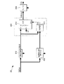
図1は、本実施形態に係る映像処理回路を適用した液晶表示装置の全体構成を示すブロ
ック図である。
この図に示されるように、液晶表示装置1は、制御回路10と、液晶パネル100と、
走査線駆動回路130と、データ線駆動回路140とを有する。
このうち、制御回路10には、映像信号Vid-inが、上位装置から同期信号Syncに同期
して供給される。映像信号Vid-inは、液晶パネル100における各画素の階調レベルを
それぞれ指定するデジタルデータであり、同期信号Syncに含まれる垂直走査信号、水平
走査信号およびドットクロック信号(いずれも図示省略)にしたがった走査の順番で供給
される。
なお、映像信号Vid-inは階調レベルを指定するが、階調レベルに応じて液晶素子の印
加電圧が定まるので、映像信号Vid-inは液晶素子の印加電圧を指定するものといって差
し支えない。
<First Embodiment>
Embodiments of the present invention will be described below with reference to the drawings.
FIG. 1 is a block diagram showing an overall configuration of a liquid crystal display device to which a video processing circuit according to this embodiment is applied.
As shown in this figure, the liquid
The scanning
Among these, the video signal Vid-in is supplied to the
The video signal Vid-in designates the gradation level, but since the applied voltage of the liquid crystal element is determined according to the gradation level, the video signal Vid-in can be said to designate the applied voltage of the liquid crystal element. Absent.
制御回路10は、走査制御回路20と映像処理回路30とにより構成され、このうち、
走査制御回路20は、各種の制御信号を生成して、同期信号Syncに同期して各部を制御
する。映像処理回路30は、詳細については後述するが、デジタルの映像信号Vid-inを
処理して、アナログのデータ信号Vxを出力するものである。
The
The
液晶パネル100は、素子基板(第1基板)100aと対向基板(第2基板)100b
とが一定の間隙を保って貼り合わせられるとともに、この間隙に、縦方向の電界で駆動さ
れる液晶105が挟持された構成となっている。
素子基板100aのうち、対向基板100bとの対向面には、複数m行の走査線112
が図においてX(横)方向に沿って設けられる一方、複数n列のデータ線114が、Y(
縦)方向に沿って、かつ、各走査線112と互いに電気的に絶縁を保つように設けられて
いる。
なお、本実施形態では、走査線112を区別するために、図において上から順に1、2
、3、…、(m−1)、m行目という呼び方をする場合がある。同様に、データ線114
を区別するために、図において左から順に1、2、3、…、(n−1)、n列目という呼
び方をする場合がある。
The
And a
Of the
Are provided along the X (horizontal) direction in the figure, while a plurality of n columns of
Along the (vertical) direction, each
In this embodiment, in order to distinguish the
3,..., (M−1), m-th line may be called. Similarly,
In order to distinguish these, there are cases where they are referred to as 1, 2, 3,..., (N−1), n-th column in order from the left in the figure.
素子基板100aでは、さらに、走査線112とデータ線114との交差のそれぞれに
対応して、nチャネル型のTFT116と矩形形状で透明性を有する画素電極118との
組が設けられている。TFT116のゲート電極は走査線112に接続され、ソース電極
はデータ線114に接続され、ドレイン電極が画素電極118に接続されている。
一方、対向基板100bのうち、素子基板100aとの対向面には、透明性を有するコ
モン電極108が全面にわたって設けられる。コモン電極108には、図示省略した回路
によって電圧LCcomが印加される。
なお、図1において、素子基板100aの対向面は紙面裏側であるので、当該対向面に
設けられる走査線112、データ線114、TFT116および画素電極118について
は、破線で示すべきであるが、見難くなるので、それぞれ実線で示している。
In the
On the other hand, a transparent
In FIG. 1, since the facing surface of the
液晶パネル100における等価回路は、図2に示される通りとなり、走査線112とデ
ータ線114との交差に対応して、画素電極118とコモン電極108とで液晶105を
挟持した液晶素子120が配列した構成となる。
また、図1では省略したが、液晶パネル100における等価回路では、実際には図2に
示されるように、液晶素子120に対して並列に補助容量(蓄積容量)125が設けられ
る。この補助容量125は、一端が画素電極118に接続され、他端が容量線115に共
通接続されている。容量線115は時間的に一定の電圧に保たれている。
ここで、走査線112がHレベルになると、当該走査線にゲート電極が接続されたTF
T116がオンとなり、画素電極118がデータ線114に接続される。このため、走査
線112がHレベルであるときに、データ線114に階調に応じた電圧のデータ信号を供
給すると、当該データ信号は、オンしたTFT116を介して画素電極118に印加され
る。走査線112がLレベルになると、TFT116はオフするが、画素電極に印加され
た電圧は、液晶素子120の容量性および補助容量125によって保持される。
液晶素子120では、画素電極118およびコモン電極108によって生じる電界に応
じて液晶105の分子配向状態が変化する。このため、液晶素子120は、透過型であれ
ば、印加・保持電圧に応じた透過率となる。
液晶パネル100では、液晶素子120毎に透過率が変化するので、液晶素子120が
画素に相当する。そして、この画素の配列領域が表示領域101となる。なお、本実施形
態において、液晶105をVA方式として、液晶素子120が電圧無印加時において黒状
態となるノーマリーブラックモードとする。
The equivalent circuit in the
Although omitted in FIG. 1, in the equivalent circuit in the
Here, when the
T116 is turned on, and the
In the
In the
走査線駆動回路130は、走査制御回路20による制御信号Yctrにしたがって、1、
2、3、…、m行目の走査線112に、走査信号Y1、Y2、Y3、…、Ymを供給する
。詳細には、走査線駆動回路130は、図5の(a)に示されるように、走査線112を
フレームにわたって1、2、3、…、(m−1)、m行目という順番で選択するとともに
、選択した走査線への走査信号を選択電圧VH(Hレベル)とし、それ以外の走査線への
走査信号を非選択電圧VL(Lレベル)とする。
なお、フレームとは、液晶パネル100を駆動することによって、画像の1コマ分を表
示させるのに要する期間をいい、同期信号Syncに含まれる垂直走査信号の周波数が60
Hzであれば、その逆数である16.7ミリ秒である。
The scanning
The scanning signals Y1, Y2, Y3,..., Ym are supplied to the
The frame means a period required to display one frame of an image by driving the
If it is Hz, the reciprocal is 16.7 milliseconds.
データ線駆動回路140は、映像処理回路30から供給されるデータ信号Vxを、走査
制御回路20による制御信号Xctrにしたがって1〜n列目のデータ線114にデータ信
号X1〜Xnとしてサンプリングする。
なお、本説明において電圧については、液晶素子120の印加電圧を除き、特に明記し
ない限り図示省略した接地電位を電圧ゼロの基準とする。液晶素子120の印加電圧は、
コモン電極108の電圧LCcomと画素電極118との電位差であり、他の電圧と区別す
るためである。
The data line driving
It should be noted that in this description, with respect to the voltage, except for the voltage applied to the
This is a potential difference between the voltage LCcom of the
さて、本実施形態において、液晶素子120の印加電圧と透過率との関係は、ノーマリ
ーブラックモードであれば、図4の(a)に示されるようなV−T特性で表される。この
ため、液晶素子120を、映像信号Vid-inで指定された階調レベルに応じた透過率とさ
せるには、当該階調レベルに応じた電圧を、該液晶素子に印加すれば良いはずである。
しかしながら、液晶素子120の印加電圧を、映像信号Vid-inで指定される階調レベ
ルに応じて単に規定するだけでは、リバースチルトドメインに起因する表示上の不具合が
発生してしまう場合がある。
In the present embodiment, the relationship between the applied voltage and the transmittance of the
However, if the voltage applied to the
この不具合は、液晶素子120において挟持された液晶分子が不安定な状態にあるとき
に、横電界の影響によって乱れる結果、以後、印加電圧に応じた配向状態になりにくくな
ることが原因の1つとして考えられている。
液晶素子120への印加電圧が、ノーマリーブラックモードにおける黒レベルの電圧V
b k以上であって閾値Vth1(第1電圧)を下回る電圧範囲Aにあると、縦電界による規制
力が配向膜による規制力よりもわずかに上回る程度であるため、液晶分子の配向状態が乱
れやすい。これが、液晶分子が不安定な状態にあるときである。
便宜的に、液晶素子の印加電圧が電圧範囲Aにある液晶素子の透過率範囲(階調範囲)
を「a」とする。
One of the causes of this defect is that when the liquid crystal molecules sandwiched in the
The voltage applied to the
If it is in the voltage range A that is greater than or equal to bk and less than the threshold value Vth1 (first voltage), the alignment force due to the longitudinal electric field is slightly higher than the restriction force due to the alignment film, so the alignment state of the liquid crystal molecules tends to be disturbed . This is when the liquid crystal molecules are in an unstable state.
For convenience, the transmittance range (tone range) of the liquid crystal element in which the applied voltage of the liquid crystal element is in the voltage range A
Is “a”.
一方、横電界の影響を受ける場合とは、互いに隣り合う画素電極同士の電位差が大きく
なる場合であり、これは、表示しようとする画像において黒レベルまたは黒レベルに近い
暗画素と、白レベルまたは白レベルに近い明画素と、が隣接する場合である。
このうち、暗画素とは、図4の(a)のようなノーマリーブラックモードでは、印加電
圧が電圧範囲Aにある液晶素子120であり、この暗画素に対して横電界を与えるのが明
画素である。この明画素を特定するため、明画素を、印加電圧が閾値Vth2(第2電圧)
以上であってノーマリーブラックモードにおける白レベル電圧Vwt以下の電圧範囲Bにあ
る液晶素子120とする。
便宜的に、液晶素子の印加電圧が電圧範囲Bにある液晶素子の透過率範囲(階調範囲)
を「b」とする。
なお、ノーマリーブラックモードにおいて、閾値Vth1は、液晶素子の相対透過率を1
0%とさせる光学的閾値電圧であり、閾値Vth2は、液晶素子の相対透過率を90%とさ
せる光学的飽和電圧と考えてよい。
On the other hand, the case of being affected by a lateral electric field is a case where the potential difference between adjacent pixel electrodes becomes large. This is because a dark pixel close to a black level or a black level in an image to be displayed and a white level or This is a case where a bright pixel close to the white level is adjacent.
Among these, the dark pixel is the
The
For convenience, the transmittance range (gradation range) of the liquid crystal element in which the applied voltage of the liquid crystal element is in the voltage range B
Is “b”.
In the normally black mode, the threshold value Vth1 is 1 for the relative transmittance of the liquid crystal element.
It is an optical threshold voltage that is 0%, and the threshold Vth2 may be considered as an optical saturation voltage that causes the relative transmittance of the liquid crystal element to be 90%.
印加電圧が電圧範囲Aにある液晶素子は、電圧範囲Bにある液晶素子に隣接したときに
、横電界を受けてリバースチルトドメインが発生しやすい状況にある。
なお逆に、電圧範囲Bにある液晶素子は、電圧範囲Aにある液晶素子に隣接しても、縦
電界の影響が支配的であるために安定状態にあるので、電圧範囲Aの液晶素子のようにリ
バースチルトドメインが発生することはない。
When the applied voltage is in the voltage range A, when the liquid crystal element is adjacent to the voltage range B, a reverse tilt domain is likely to occur due to a lateral electric field.
Conversely, the liquid crystal element in the voltage range B is in a stable state because the influence of the vertical electric field is dominant even if it is adjacent to the liquid crystal element in the voltage range A. Thus, the reverse tilt domain does not occur.
この表示上の不具合の例について説明すると、映像信号Vid-inで示される画像が例え
ば図19の(a)に示されるようなものである場合、詳細には、階調範囲aの暗画素が階
調範囲bの明画素を背景としてフレーム毎に1画素ずつ左方向に移動する場合、暗画素か
ら明画素に変化すべき画素がリバースチルトドメインの発生によって階調範囲bの階調に
はならない、という一種の尾引き現象として顕在化する。
この現象の原因の1つとしては、暗画素と明画素とが隣接したときに、これらの画素同
士の横電界が強くなって、当該暗画素において液晶分子の配向が乱れるとともに、配向の
乱れた領域が、暗画素の移動に伴って拡大したためである考えられる。
したがって、液晶分子の配向乱れに起因する表示上の不具合の発生を抑えるためには、
映像信号Vid-inで示される画像において暗画素と明画素とが隣接するときでも、液晶パ
ネル100では、暗画素と明画素とを隣接させないことが重要となる。
An example of this display defect will be described. When the image indicated by the video signal Vid-in is, for example, as shown in FIG. When moving to the left one pixel at a time for each frame with a bright pixel in the gradation range b as a background, a pixel that should change from a dark pixel to a bright pixel does not become a gradation in the gradation range b due to the occurrence of a reverse tilt domain. It is manifested as a kind of tailing phenomenon.
One of the causes of this phenomenon is that when a dark pixel and a bright pixel are adjacent to each other, the lateral electric field between these pixels becomes strong, and the orientation of liquid crystal molecules is disturbed in the dark pixel, and the orientation is disturbed. This is considered to be because the area is enlarged as the dark pixel moves.
Therefore, in order to suppress the occurrence of display defects caused by the alignment disorder of the liquid crystal molecules,
Even when the dark pixel and the bright pixel are adjacent to each other in the image indicated by the video signal Vid-in, it is important that the dark pixel and the bright pixel are not adjacent to each other in the
そこで、本実施形態では、図1に示されるように映像処理回路30を液晶パネル100
の前段に設けるとともに、当該映像処理回路30が、映像信号Vid-inで示される画像を
解析して、階調範囲aの暗画素と階調範囲bの明画素とが隣接する状態があるか否かを検
出し、あれば、暗画素と明画素との境界に接する画素のうち、印加電圧を低くすべき方の
画素、すなわち横電界の影響を受けやすい画素(ノーマリーブラックモードでは暗画素)
の階調レベルを、階調範囲aでもなく、階調範囲bでもない別の階調範囲cに属する階調
レベルc1に置換される。これにより液晶パネル100では、当該暗画素に係る液晶素子
120に対し、当該階調レベルc1に相当する電圧Vc1が印加されるので、強い横電界が
発生しないことになる。
Therefore, in the present embodiment, as shown in FIG.
And the
Is replaced with a gradation level c1 belonging to another gradation range c that is neither the gradation range a nor the gradation range b. As a result, in the
そこで次に、映像処理回路30の詳細について図3を参照して説明する。この図に示さ
れるように、映像処理回路30は、補正部300、境界検出部302、遅延回路312お
よびD/A変換器316を有する。
このうち、遅延回路312は、上位装置から供給される映像信号Vid-inを蓄積して、
所定時間経過後に読み出して映像信号Vid-dとして出力するものであり、FIFO(Fast
In Fast Out:先入れ先出し)メモリーや多段のラッチ回路などにより構成される。なお
、遅延回路312における蓄積および読出は、走査制御回路20によって制御される。
Next, details of the
Among these, the
Reads out after a predetermined time and outputs it as a video signal Vid-d.
In Fast Out: First-in first-out) Consists of memory and multistage latch circuit. The accumulation and reading in the
境界検出部302は、本実施形態においては、第1に、映像信号Vid-inで示される画
像を解析して、階調範囲aにある画素と階調範囲bにある画素とが隣接する部分があるか
否かを判別し、第2に、隣接する部分があると判別したとき、その隣接部分である境界を
検出する。
なお、ここでいう境界とは、あくまでも階調範囲aにある画素と階調範囲bにある画素
とが隣接する部分をいう。このため、例えば階調範囲aにある画素と階調範囲cにある画
素とが隣接する部分や、階調範囲bにある画素と階調範囲cにある画素とが隣接する部分
については、境界として扱わない。
In the present embodiment, the
Note that the boundary here refers to a portion where a pixel in the gradation range a and a pixel in the gradation range b are adjacent to each other. Therefore, for example, a boundary between a pixel in the gradation range a and a pixel in the gradation range c, or a part in which a pixel in the gradation range b and a pixel in the gradation range c are adjacent, Not treated as.
補正部300は、判別部310とセレクター314とを有する。このうち、判別部31
0は、遅延回路312によって遅延された映像信号Vid-dで示される画素の階調レベルが
階調範囲aに属するか否か(第1の判別)、および、当該画素が境界検出部306で検出
された境界に接しているか否か(第2の判別)を、それぞれ判別して、その判別結果がい
ずれも「Yes」である場合に出力信号のフラグQを例えば「1」とし、その判別結果が
いずれか1つでも「No」であれば「0」とする。
なお、境界検出部302は、少なくとも複数ラインの映像信号を蓄積してからでないと
、表示すべき画像における境界を検出することができないので、映像信号Vid-inの供給
タイミングを調整する意味で、遅延回路312が設けられている。
このため、上位装置から供給される映像信号Vid-inのタイミングと、遅延回路312
から供給される映像信号Vid-dのタイミングとは異なるので、厳密にいえば、両者の水平
走査期間等については一致しないことになるが、以降については特に区別しないで説明す
る。
The
0 indicates whether or not the gradation level of the pixel indicated by the video signal Vid-d delayed by the
In addition, since the
Therefore, the timing of the video signal Vid-in supplied from the host device and the
Since the timing of the video signal Vid-d supplied from is different from the timing of the video signal Vid-d, strictly speaking, the horizontal scanning periods of the two do not coincide with each other.
セレクター314は、制御端子Selに供給されたフラグQに応じて入力端a、bのいず
れかを選択し、選択した入力端に供給された信号を出力端Outから映像信号Vid-outを出
力するものである。詳細には、セレクター314では、入力端aに、遅延回路312によ
る映像信号Vid-dが供給され、入力端bに、置換用として、階調レベルc1の映像信号が
供給されている。そして、セレクター314は、制御端子Selに供給されたフラグQが「
1」であれば、入力端bを選択し、該フラグQが「0」であれば、入力端aに供給された
映像信号Vid-dを映像信号Vid-outとして出力する。
The
If “1”, the input terminal b is selected, and if the flag Q is “0”, the video signal Vid-d supplied to the input terminal a is output as the video signal Vid-out.
D/A変換器316は、デジタルデータである映像信号Vid-outを、アナログのデータ
信号Vxに変換する。
液晶105に直流成分が印加されるのを防止するため、データ信号Vxの電圧は、ビデ
オ振幅中心である電圧Vcに対して高位側の正極性電圧と低位側の負極性電圧とに例えば
フレーム毎に交互に切り替えられる。
なお、コモン電極108に印加される電圧LCcomは、電圧Vcとほぼ同電圧と考えてよ
いが、nチャネル型のTFT116のオフリーク等を考慮して、電圧Vcよりも低位とな
るように調整されることがある。
The D /
In order to prevent the direct current component from being applied to the
Note that the voltage LCcom applied to the
このような構成において、フラグQが「1」であれば、それは、映像信号Vid-inで示
される画素の階調レベルが階調範囲aに含まれ、かつ、当該画素が明画素との境界に接し
ている、ということ、すなわち境界を挟んで隣接する明画素から横電界の影響を受けてリ
バースチルトドメインが発生しやすい状況にあることを、を意味している。
フラグQが「1」であれば、セレクター314が入力端bを選択するので、階調範囲a
の階調レベルを指定する映像信号Vid-dは、階調レベルc1を指定する映像信号に置換さ
れて、映像信号Vid-outとして出力される。
一方、フラグQが「0」であれば、セレクター314では、入力端aが選択されるので
、遅延させた映像信号Vid-dが映像信号Vid-outとして出力される。
In such a configuration, if the flag Q is “1”, it means that the gradation level of the pixel indicated by the video signal Vid-in is included in the gradation range a and the pixel is a boundary with the bright pixel. That is, the reverse tilt domain is likely to occur due to the influence of the lateral electric field from the adjacent bright pixels across the boundary.
If the flag Q is “1”, the
The video signal Vid-d designating the gray level is replaced with the video signal designating the gray level c1 and output as the video signal Vid-out.
On the other hand, if the flag Q is “0”, the
液晶表示装置1の表示動作について説明すると、上位装置からは、映像信号Vid-inが
、フレームにわたって1行1列〜1行n列、2行1列〜2行n列、3行1列〜3行n列、
…、m行1列〜m行n列の画素の順番で、供給される。映像処理回路30は、映像信号V
id-inを遅延・置換等の処理をして映像信号Vid-outとして出力する。
ここで、1行1列〜1行n列の映像信号Vid-outが出力される水平有効走査期間(Ha
)でみたときに、処理された映像信号Vid-outは、D/A変換器316によって、図5の
(b)で示されるように正極性または負極性のデータ信号Vxに、ここでは例えば正極性
に変換される。このデータ信号Vxは、データ線駆動回路140によって1〜n列目のデ
ータ線114にデータ信号X1〜Xnとしてサンプリングされる。
一方、1行1列〜1行n列の映像信号Vid-outが出力される水平走査期間では、走査制
御回路20が走査線駆動回路130に対し走査信号Y1だけをHレベルとなるように制御
する。走査信号Y1がHレベルであれば、1行目のTFT116がオン状態になるので、
データ線114にサンプリングされたデータ信号は、オン状態にあるTFT116を介し
て画素電極118に印加される。これにより、1行1列〜1行n列の液晶素子には、それ
ぞれ映像信号Vid-outで指定された階調レベルに応じた正極性電圧が書き込まれる。
続いて、2行1列〜2行n列の映像信号Vid-inは、同様に映像処理回路30によって
処理されて、映像信号Vid-outとして出力されるとともに、D/A変換器316によって
正極性のデータ信号に変換された上で、データ線駆動回路140によって1〜n列目のデ
ータ線114にサンプリングされる。
2行1列〜2行n列の映像信号Vid-outが出力される水平走査期間では、走査線駆動回
路130によって走査信号Y2だけがHレベルとなるので、データ線114にサンプリン
グされたデータ信号は、オン状態にある2行目のTFT116を介して画素電極118に
印加される。これにより、2行1列〜2行n列の液晶素子には、それぞれ映像信号Vid-o
utで指定された階調レベルに応じた正極性電圧が書き込まれる。
以下同様な書込動作が3、4、…、m行目に対して実行され、これにより、各液晶素子
に、映像信号Vid-outで指定された階調レベルに応じた電圧が書き込まれて、映像信号V
id-inで規定される透過像が作成されることなる。
次のフレームでは、データ信号の極性反転によって映像信号Vid-outが負極性のデータ
信号に変換される以外、同様な書込動作が実行される。
The display operation of the liquid
..., supplied in the order of pixels of m rows and 1 column to m rows and n columns. The
The id-in is subjected to processing such as delay and replacement, and is output as a video signal Vid-out.
Here, a horizontal effective scanning period (Ha) in which the video signal Vid-out of 1
), The processed video signal Vid-out is converted into a positive or negative data signal Vx by a D /
On the other hand, in the horizontal scanning period in which the video signal Vid-out of 1
The data signal sampled on the
Subsequently, the video signal Vid-in in the 2nd row and the 1st column to the 2nd row and the nth column is similarly processed by the
In the horizontal scanning period in which the video signal Vid-out of the 2nd row and the 1st column to the 2nd row and the nth column is output, only the scanning signal Y2 is set to the H level by the scanning
A positive voltage corresponding to the gradation level specified by ut is written.
Thereafter, a similar writing operation is executed for the third, fourth,..., M-th rows, whereby a voltage corresponding to the gradation level specified by the video signal Vid-out is written to each liquid crystal element. Video signal V
A transmission image defined by id-in is created.
In the next frame, a similar writing operation is executed except that the video signal Vid-out is converted into a negative polarity data signal by polarity inversion of the data signal.
図5の(b)は、映像処理回路30から、水平走査期間(H)にわたって1行1列〜1
行n列の映像信号Vid-outが出力されたときのデータ信号Vxの一例を示す電圧波形図で
ある。本実施形態では、ノーマリーブラックモードとしているので、データ信号Vxは、
正極性であれば、基準電圧Vcntに対し、映像処理回路30によって処理された階調レベ
ルに応じた分だけ高位側の電圧(図において↑で示す)になり、負極性であれば、基準電
圧Vcntに対し、階調レベルに応じた分だけ低位側の電圧(図において↓で示す)になる
。
詳細には、データ信号Vxの電圧は、正極性であれば、白に相当する電圧Vw(+)から黒
に相当する電圧Vb(+)までの範囲で、一方、負極性であれば、白に相当する電圧Vw(-)か
ら黒に相当する電圧Vb(-)までの範囲で、それぞれ基準電圧Vcntから階調に応じた分だ
け偏位させた電圧となる。
電圧Vw(+)および電圧Vw(-)は、電圧Vcntを中心に互いに対称の関係にある。電圧Vb
(+)およびVb(-)についても電圧Vcntを中心に互いに対称の関係にある。
なお、図5の(b)は、データ信号Vxの電圧波形を示すものであって、液晶素子12
0に印加される電圧(画素電極118とコモン電極108との電位差)とは異なる。また
、図5の(b)におけるデータ信号の電圧の縦スケールは、(a)における走査信号等の
電圧波形と比較して拡大してある。
(B) of FIG. 5 shows from the
It is a voltage waveform diagram showing an example of the data signal Vx when the video signal Vid-out of row n column is output. In this embodiment, since the normally black mode is used, the data signal Vx is
If the polarity is positive, the reference voltage Vcnt is higher than the reference voltage Vcnt by the gradation level processed by the video processing circuit 30 (indicated by ↑ in the figure). If the polarity is negative, the reference voltage is With respect to Vcnt, it becomes a lower voltage (indicated by ↓ in the figure) corresponding to the gradation level.
Specifically, if the voltage of the data signal Vx is positive, the voltage ranges from the voltage Vw (+) corresponding to white to the voltage Vb (+) corresponding to black. In the range from the voltage Vw (−) corresponding to 1 to the voltage Vb (−) corresponding to black, the voltages are shifted from the reference voltage Vcnt by the amount corresponding to the gradation.
The voltage Vw (+) and the voltage Vw (−) are in a symmetric relationship with respect to the voltage Vcnt. Voltage Vb
(+) And Vb (−) are also symmetrical with respect to the voltage Vcnt.
FIG. 5B shows the voltage waveform of the data signal Vx, and the liquid crystal element 12.
The voltage applied to 0 (potential difference between the
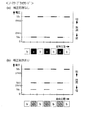
第1実施形態に係る映像処理回路30による処理の具体例について説明する。
映像信号Vid-inで示される画像が例えば図6の(1)に示されるようなものである場
合、境界検出部302によって検出される境界は、図6の(2)に示される。
映像処理回路30では、検出された境界に接する画素のうち、階調レベルが階調範囲a
に属する画素が階調レベルc1の映像信号に置換される。このため、図6の(1)で示さ
れる画像は、映像処理回路30によって図6の(3)に示されるような階調レベルに補正
される。
A specific example of processing by the
When the image indicated by the video signal Vid-in is, for example, as shown in (1) of FIG. 6, the boundary detected by the
In the
Are replaced with video signals of gradation level c1. For this reason, the image shown in (1) of FIG. 6 is corrected by the
仮に、映像信号Vid-inを映像処理回路30で処理しないで液晶パネル100に供給す
る構成としたとき、階調範囲aに属する暗画素と階調範囲bに属する明画素とにおいて、
画素電極の電位は、正極性書込であれば、図7の(a)で示される通りとなる。すなわち
、暗画素の画素電極の電位は、正極性書込であれば明画素の画素電極の電位よりも低くな
るが、その電位差が大きいので、横電界の影響をうけやすくなる。
なお、負極性であれば、電圧Vc(ほぼ電圧LCcomに等しい)を基準にして対称となり
、電位の高低関係が逆転するが、電位差が大きいことに変わりはないので、やはり横電界
の影響をうけやすくなる。
これに対し、本実施形態のように、映像信号Vid-inで示される画像において、階調範
囲aに属する暗画素と階調範囲bに属する明画素とが隣接するとき、暗画素に対応する映
像信号Vid-outは、階調レベルc1に置換されるので、当該暗画素の液晶素子への印加電
圧は高くなるように、換言すれば、当該暗画素の画素電極の電位は、正極性書込であれば
、図7の(b)で示されるように引き上げられる。
このため、画素電極同士の電位差が段階的に変化するので、横電界の影響を小さく抑え
ることが可能となる。
Assuming that the video signal Vid-in is supplied to the
In the case of positive polarity writing, the potential of the pixel electrode is as shown in FIG. That is, the potential of the pixel electrode of the dark pixel is lower than the potential of the pixel electrode of the bright pixel in the case of positive writing, but since the potential difference is large, it is easily affected by the lateral electric field.
In the case of negative polarity, the voltage Vc (substantially equal to the voltage LCcom) is symmetric and the potential level relationship is reversed, but the potential difference is still large, so it is still affected by the lateral electric field. It becomes easy.
On the other hand, when the dark pixel belonging to the gradation range a and the bright pixel belonging to the gradation range b are adjacent to each other in the image indicated by the video signal Vid-in as in the present embodiment, it corresponds to the dark pixel. Since the video signal Vid-out is replaced with the gradation level c1, the voltage applied to the liquid crystal element of the dark pixel is increased, in other words, the potential of the pixel electrode of the dark pixel is a positive polarity document. If it is included, it is pulled up as shown in FIG.
For this reason, since the potential difference between the pixel electrodes changes stepwise, the influence of the lateral electric field can be kept small.
なお、図8の(a)に示されるように、映像信号Vid-inで示される画像が、階調範囲
aに属する暗画素と階調範囲bに属する明画素とを交互に配列した画像である場合、映像
処理回路30による処理がなければ、液晶素子120の印加電圧は同図に示される通りと
なり、横電界の影響を受けやすくなる。
これに対し、本実施形態のように、映像信号Vid-inを映像処理回路30によって処理
して液晶パネル100に供給する構成では、図8の(b)に示されるように、階調範囲a
に属する暗画素の液晶素子120への印加電圧が階調レベルc1に対応して電圧Vc1に引
き上げられるので、横電界の影響を小さく抑えることが可能となる。
なお、このとき、暗画素の液晶素子への印加電圧は、電圧Vc1に引き上げられる結果、
その透過率は大きくなる(明るくなる)方向に変化する。
As shown in FIG. 8A, the image represented by the video signal Vid-in is an image in which dark pixels belonging to the gradation range a and bright pixels belonging to the gradation range b are alternately arranged. In some cases, if there is no processing by the
On the other hand, in the configuration in which the video signal Vid-in is processed by the
Since the voltage applied to the
At this time, the voltage applied to the liquid crystal element of the dark pixel is raised to the voltage Vc1,
The transmittance changes in the direction of increasing (brightening).
本実施形態において、液晶105をVA方式としたノーマリーブラックモードとして説
明したが、液晶105を例えばTN方式として、電圧無印加時において液晶素子120が
白状態となるノーマリーホワイトモードとしてもよい。
ノーマリーホワイトモードとしたとき、液晶素子120の印加電圧と透過率との関係は
、図4の(b)に示されるようなV−T特性で表され、印加電圧が高くなるにつれて透過
率が減少する。
横電界の影響を受ける画素は、印加電圧が低い方の画素であることに変わりはないが、
ノーマリーホワイトモードにおいて印加電圧が低い方の画素は明画素となる。
このため、ノーマリーホワイトモードにおいて、映像処理回路30は、印加電圧が閾値
Vth1であるときの透過率よりも大きい明画素と印加電圧が閾値Vth2であるときの透過率
以下の暗画素とが隣接するような状況である場合に、映像信号Vid-inで指定される明画
素の階調レベルを、階調レベルc1に置換する処理をすれば良いことになる。
図9の(a)に示されるように、映像信号Vid-inで示される画像が、明画素と暗画素
とを交互に配列した画像である場合、映像処理回路30による補正処理がなければ、液晶
素子120の印加電圧は同図に示される通りとなり、同様に、横電界の影響を受けやすく
なる。
これに対し、映像信号Vid-inを映像処理回路30によって処理して液晶パネル100
に供給する構成では、図9の(b)に示されるように、明画素の液晶素子120への印加
電圧が階調レベルc1に対応して電圧Vc1に引き上げられるので、横電界の影響を小さく
抑えることが可能となる。
このとき、明画素の液晶素子への印加電圧は、電圧Vc1に引き上げられる結果、その透
過率は小さくなる(暗くなる)方向に変化する。
In the present embodiment, the
In the normally white mode, the relationship between the applied voltage and the transmittance of the
The pixel affected by the lateral electric field is still the pixel with the lower applied voltage,
In the normally white mode, the pixel with the lower applied voltage is a bright pixel.
For this reason, in the normally white mode, the
As shown in FIG. 9A, when the image indicated by the video signal Vid-in is an image in which bright pixels and dark pixels are alternately arranged, if there is no correction processing by the
On the other hand, the video signal Vid-in is processed by the
9B, the voltage applied to the
At this time, as a result of raising the voltage applied to the liquid crystal element of the bright pixel to the voltage Vc1, the transmittance changes in a direction of decreasing (darkening).
このように、本実施形態によれば、上述したリバースチルトドメインに起因する表示上
の不具合の発生を事前に回避することが可能となる。さらに、映像信号Vid-inで規定さ
れる画像のうち、境界に接する画素の階調レベルが局所的に置換されるので、当該置換に
よる表示画像の変更がユーザーに知覚される可能性も小さい。くわえて、本実施形態では
、液晶パネル100の構造を変更する必要がないので、開口率の低下を招くこともないし
、また、構造を工夫しないで既に製作された液晶パネルに適用することも可能である。
As described above, according to the present embodiment, it is possible to avoid in advance the occurrence of display defects due to the above-described reverse tilt domain. Furthermore, in the image defined by the video signal Vid-in, the gradation level of the pixel in contact with the boundary is locally replaced, so that the possibility that the change of the display image due to the replacement is perceived by the user is small. In addition, in this embodiment, since it is not necessary to change the structure of the
なお、図6の(3)において、※1で記した暗画素については、境界に接している、と
考えて、階調レベルc1に置換するとしたが、明画素とは対角の位置にあるので、横電界
の影響は小さいと考えられる。このため、階調レベルc1に置換しない構成としても良い
。
In FIG. 6 (3), the dark pixel marked with * 1 is considered to be in contact with the boundary and is replaced with the gradation level c1, but it is at a diagonal position with respect to the bright pixel. Therefore, the influence of the transverse electric field is considered to be small. For this reason, it is good also as a structure which is not substituted by the gradation level c1.
<第1実施形態の応用・変形例>
上述した第1実施形態では、種々の応用・変形が可能である。
<Application / Modification of First Embodiment>
In the first embodiment described above, various applications and modifications are possible.
<その1>
上述した第1実施形態では、映像信号Vid-inの解析によって暗画素と明画素とが隣接
するとき、当該2画素のうち、印加電圧を低くすべき方の1画素(ノーマリーブラックモ
ードでは暗画素)を、階調範囲cに属する階調レベルc1に置換することによって、液晶
素子120の印加電圧を高くする構成とした。この構成では、階調レベルc1への置換に
よって暗画素と明画素との境界が、映像信号Vid-inに含まれていた境界からシフトして
、ユーザーに視認されてしまう可能性がある。
そこで、リバースチルトドメインに起因する表示上の不具合の発生を事前に回避しつつ
、境界がシフトして視認される可能性を小さく抑えるために、当該境界に接する2画素を
補正する第1実施形態の応用・変形例(その1)について説明する。
<
In the first embodiment described above, when a dark pixel and a bright pixel are adjacent to each other by analysis of the video signal Vid-in, one of the two pixels whose applied voltage is to be lowered (dark in the normally black mode). The pixel is replaced with a gradation level c1 belonging to the gradation range c, so that the voltage applied to the
Therefore, in order to prevent the occurrence of display defects caused by the reverse tilt domain in advance and suppress the possibility that the boundary is shifted and visually recognized, the first embodiment for correcting two pixels in contact with the boundary is corrected. An application / variation example (No. 1) will be described.
図10は、第1実施形態の応用・変形例に係る映像処理回路の構成を示すブロック図で
ある。図10に示される構成が図3に示した構成と相違する部分は、算出部315が追加
された点と、判別部310の判別内容が変更された点とにある。
詳細には、ノーマリーブラックモードを例にとると、算出部315は、遅延された映像
信号Vid-dの画素が境界検出部302によって検出された境界に接している場合に、第1
に、当該画素が暗画素であれば階調レベルcaを出力し、第2に、当該画素が明画素であ
れば、階調レベルcbを算出して出力するものである。なお、階調レベルcbについて算出
部315は、映像信号Vid-dで指定される明画素の階調レベル、境界を挟んで対向する暗
画素の階調レベル、および、階調レベルcaから算出する。
ここで、階調レベルcaは、データ線駆動回路140によってデータ信号に変換して画
素電極に印加したときに、その液晶素子の印加電圧を電圧範囲CにあるVcaとさせる階調
レベルである。また、算出部315が算出する階調レベルcbは、映像信号Vid-inにおい
て暗画素と明画素とが隣接する場合に、暗画素を階調レベルcaに置換し、明画素を階調
レベルcbに置換したとき、信号Vid-inにおける暗画素と明画素との境界情報を維持する
ような階調レベルであって、明画素にかかる液晶素子の印加電圧を印加電圧Vcaよりも大
きい電圧Vcbとさせる階調レベルである。
FIG. 10 is a block diagram illustrating a configuration of a video processing circuit according to an application / modification of the first embodiment. The difference between the configuration shown in FIG. 10 and the configuration shown in FIG. 3 is that the calculation unit 315 is added and the determination content of the
Specifically, taking the normally black mode as an example, the calculation unit 315 performs the first operation when the pixel of the delayed video signal Vid-d is in contact with the boundary detected by the
If the pixel is a dark pixel, the tone level ca is output. Second, if the pixel is a bright pixel, the tone level cb is calculated and output. Note that the calculation unit 315 calculates the gradation level cb from the gradation level of the bright pixel specified by the video signal Vid-d, the gradation level of the dark pixel opposed across the boundary, and the gradation level ca. .
Here, the gradation level ca is a gradation level at which the voltage applied to the liquid crystal element is set to Vca in the voltage range C when converted to a data signal by the data line driving
図10における判別部310は、図3とは異なり、第2の判別のみ、遅延した映像信号
Vid-dで示される画素が境界検出部306で検出された境界に接しているか否かについて
のみ判別する。判別部310は、その判別結果が「Yes」である場合に出力信号のフラ
グQを例えば「1」とし、その判別結果が「No」であれば「0」とする点については、
図3と同様である。
The
This is the same as FIG.
このような構成において、フラグQが「1」であれば、それは、映像信号Vid-dの画素
が境界に接している、ということである。フラグQが「1」であれば、セレクター314
が入力端bを選択するので、映像信号Vid-dは、算出部315から出力される階調レベル
に補正(置換)されて映像信号Vid-outとして出力される。
検出された境界には、電圧範囲A(階調レベルa)となる暗画素と電圧範囲B(階調レ
ベルb)となる明画素とが隣接しているが、算出部315は、このうち暗画素であれば階
調レベルcaを出力し、明画素でなれば階調レベルcbを算出して出力する。
In such a configuration, if the flag Q is “1”, it means that the pixel of the video signal Vid-d is in contact with the boundary. If the flag Q is “1”, the
Select the input end b, the video signal Vid-d is corrected (replaced) to the gradation level output from the calculation unit 315 and output as the video signal Vid-out.
A dark pixel in the voltage range A (tone level a) and a bright pixel in the voltage range B (tone level b) are adjacent to the detected boundary. If the pixel is a pixel, the gradation level ca is output. If the pixel is not a bright pixel, the gradation level cb is calculated and output.
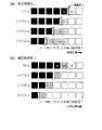
図10に示した映像処理回路30による補正処理の具体例について説明する。
映像信号Vid-inで示される画像が例えば図11の(1)に示されるようなものである
場合、境界検出部302によって検出される境界は、図11の(2)に示される通りであ
り、ここまでは、図3に示した映像処理回路と同様である。
図10に示した映像処理回路30では、遅延した映像信号Vid- dの画素が境界に接す
る場合に、当該画素が暗画素であれば階調レベルcaに、当該画素が明画素であれば階調
レベルcbに、それぞれ置換される。このため、図10の(1)で示される画像は、映像
処理回路30によって図10の(3)に示されるような階調レベルに補正される。
A specific example of correction processing by the
When the image indicated by the video signal Vid-in is, for example, as shown in (1) of FIG. 11, the boundary detected by the
In the
仮に、映像信号Vid-inで示される画像のうち、1行の一部において、図12(a)で
示されるように、階調範囲aに属する暗画素と階調範囲bに属する明画素とが配列する状
態を想定する。
図3に示した映像処理回路では、境界に接する暗画素が階調レベルc1に置き換わるの
で、図7の(b)に示されるように、ユーザーに視認される暗画素と明画素との輪郭は、
暗画素寄りにシフトする。
これに対して、図10に示した応用・変形例に係る映像処理回路30によれば、境界に
接する暗画素が明るい方向の階調レベルcaに置換されるので、画素電極の電位が、正極
性書込であれば、図12の(b)で示されるように引き上げられる。さらに、境界に接す
る明画素が暗い方向の階調レベルcbに置換されるので、画素電極の電位が、正極性書込
であれば、図12の(b)で示されるように引き下げられる。階調レベルcbに置換され
た場合に、画素電極の電位が、正極性書込であれば、引き上げられた暗画素よりも低い電
位であるから、ユーザーに視認される暗画素と明画素との輪郭部分は、図12の(b)に
示されるように、ほとんどシフトしない。
したがって、第1実施形態の応用・変形例に係る映像処理回路によれば、リバースチル
トドメインに起因する表示上の不具合の発生を事前に回避しつつ、ユーザーに視認される
輪郭部分が映像信号Vid-inで示される画像からシフトしてしまうことを抑えることも可
能となる。
なお、リバースチルトドメインは、一旦発生すると、縦電界が弱い部分にわたって拡が
る傾向がある。このため、横電界が強くなる境界付近にある画素については、1画素より
も2画素、2画素よりも3画素以上のように、より多くの画素にわたって補正することが
好ましい。
Temporarily, in a part of one row of the image indicated by the video signal Vid-in, as shown in FIG. 12A, a dark pixel belonging to the gradation range a and a bright pixel belonging to the gradation range b Assume a state in which is arranged.
In the video processing circuit shown in FIG. 3, since the dark pixel in contact with the boundary is replaced with the gradation level c1, as shown in FIG. 7B, the contour of the dark pixel and the bright pixel visually recognized by the user is ,
Shift toward dark pixels.
On the other hand, according to the
Therefore, according to the video processing circuit according to the application / modification of the first embodiment, the contour portion visually recognized by the user is avoided while the occurrence of the display defect due to the reverse tilt domain is avoided in advance. It is also possible to suppress shifting from the image indicated by -in.
Note that once the reverse tilt domain occurs, it tends to spread over a portion where the vertical electric field is weak. For this reason, it is preferable to correct over a larger number of pixels, such as two pixels than one pixel and three or more pixels than two pixels, in the vicinity of the boundary where the lateral electric field becomes strong.
<その2>
上述した第1実施形態では、映像信号Vid-inの解析によって暗画素と明画素とが隣接
するとき、印加電圧が低い方の画素を階調範囲cに属する階調レベルc1に置換すること
によって、液晶素子120の印加電圧を高くして、横電界が小さくなるように補正した。
横電界を小さくするには、このほかに、印加電圧が高い方画素の印加電圧を低くすること
が考えられる。
このため、第1実施形態における判別部310が、映像信号Vid-dで示される画素の階
調レベルが階調範囲bに属する明画素であるか否か、および、当該画素が境界に接してい
るか否か(第2の判別)を、それぞれ判別して、その判別結果がいずれも「Yes」であ
る場合に出力信号のフラグQを「1」とし、セレクター314の入力端bに、置換用とし
て階調レベルccの映像信号を供給する構成とすれば良い。
仮に、映像信号Vid-inを映像処理回路30で処理しないで液晶パネル100に供給す
る構成としたとき、階調範囲aに属する暗画素と階調範囲bに属する明画素とにおいて、
画素電極の電位は、正極性書込であれば、図13の(a)で示される通りとなり、暗画素
と明画素との間における横電界が大きくなる。
これに対して本例では、図13の(b)に示されるように、明画素の液晶素子への印加
電圧が低くなるように補正されるので、横電界の影響を小さく抑えることが可能となる。
<
In the first embodiment described above, when a dark pixel and a bright pixel are adjacent to each other by analysis of the video signal Vid-in, the pixel having the lower applied voltage is replaced with the gradation level c1 belonging to the gradation range c. The voltage applied to the
In order to reduce the lateral electric field, it is also conceivable to lower the applied voltage of the pixel having the higher applied voltage.
Therefore, the
Assuming that the video signal Vid-in is supplied to the
In the case of positive polarity writing, the potential of the pixel electrode is as shown in FIG. 13A, and the lateral electric field between the dark pixel and the bright pixel increases.
On the other hand, in this example, as shown in FIG. 13B, the correction is made so that the voltage applied to the liquid crystal element of the bright pixel is lowered, so that the influence of the lateral electric field can be suppressed to a low level. Become.
<第2実施形態>
上述した第1実施形態では、応用・変形例も含めて、映像信号Vid-inで示される画像
の1フレームで完結する処理であったが、動きを伴う画像である場合、上位装置から供給
される映像信号Vid-inで示されるフレーム(現フレーム)において境界に接する画素で
あっても、その現フレームよりも1つ前のフレーム(前フレーム)を含めた動きを考える
と、補正する必要がないときがある。
そこで次に、現フレームの補正に際し、前のフレームの状態を考慮する第2実施形態に
係る映像処理回路について説明する。
Second Embodiment
In the first embodiment described above, the processing is completed in one frame of the image indicated by the video signal Vid-in, including applications and modifications. However, in the case of an image with motion, it is supplied from the host device. Even if the pixel is in contact with the boundary in the frame (current frame) indicated by the video signal Vid-in, it is necessary to correct it in consideration of the motion including the previous frame (previous frame) before the current frame. There is no time.
Therefore, a video processing circuit according to the second embodiment that considers the state of the previous frame when correcting the current frame will be described next.
図14は、第2実施形態に係る映像処理回路の構成を示すブロック図である。
この図と図3に示した構成とが相違する部分は、図14では、図3に示した構成と比較
して、適用境界決定部304、境界検出部306と、保存部308とが追加されている点
と、判別部310の判別内容が変更された点とにある。
なお、境界検出部302は、図3と同様であるが、現フレームの映像信号Vid-inを処
理することから、第1境界検出部に相当することになる。
FIG. 14 is a block diagram illustrating a configuration of a video processing circuit according to the second embodiment.
14 differs from the configuration shown in FIG. 3 in that an application
The
また、境界検出部306は、映像信号Vid-inで示される画像を解析して、階調範囲a
にある画素と階調範囲bにある画素とが隣接する部分を境界として検出する。
保存部308は、境界検出部306によって検出された境界の情報を保存して1フレー
ム期間だけ遅延させて出力するものである。
したがって、境界検出部302で検出される境界は現フレームに係るものであるのに対
し、境界検出部306で検出されて保存部308に保存される境界は、現フレームの1つ
前のフレームに係るものとなる。このため、境界検出部306が第2境界検出部に相当す
ることになる。
Further, the
, And a portion where a pixel in the gradation range b is adjacent is detected as a boundary.
The
Accordingly, the boundary detected by the
適用境界決定部304は、境界検出部306によって検出された現フレーム画像の境界
のうち、保存部308に保存された前フレーム画像の境界と同じ部分を除外したものを、
適用境界として決定するものである。
判別部310は、遅延した映像信号Vid-dで示される画素の階調レベルが階調範囲aに
属するか否か、および、当該画素が適用境界決定部304で決定された適用境界に接して
いるか否かを、それぞれ判別して、その判別結果がいずれも「Yes」である場合に出力
信号のフラグQを例えば「1」とし、その判別結果がいずれか1つでも「No」であれば
「0」とする。
The application
It is determined as an application boundary.
The
この構成において、フラグQが「1」であれば、それは、遅延した映像信号Vid-dの画
素は、階調範囲aに属し、かつ、現フレームでは境界に接しているが、1フレーム前では
、境界に接していなかった、ということを意味している。フラグQが「1」であれば、セ
レクター314が入力端bを選択するので、現フレームの映像信号Vid-dは、階調レベル
c1を指定する映像信号に置換されて、映像信号Vid-outとして出力される。
一方、フラグQが「0」であれば、それは、遅延した映像信号Vid-dの画素が、
(a)階調範囲aに属していない、
(b)階調範囲aに属し、かつ、現フレームでは境界に接しており、かつ、1フレーム前
でも、境界に接していた、
のいずれかである。フラグQが「0」であれば、入力端aに供給された映像信号Vid-d
が映像信号Vid-outとして出力される。
In this configuration, if the flag Q is “1”, it means that the pixel of the delayed video signal Vid-d belongs to the gradation range a and is in contact with the boundary in the current frame, but one frame before. , Which means it was not touching the border. If the flag Q is “1”, the
On the other hand, if the flag Q is “0”, it means that the pixel of the delayed video signal Vid-d is
(A) does not belong to the gradation range a,
(B) belongs to the gradation range a, touches the boundary in the current frame, and touches the boundary even one frame before,
One of them. If the flag Q is “0”, the video signal Vid-d supplied to the input terminal a
Is output as the video signal Vid-out.
図14に示した映像処理回路30による補正処理の具体例について説明する。
現フレームに対し1フレーム前の映像信号で示される画像が例えば図15の(1)に示
される通りであって、現フレームの映像信号Vid-inで示される画像が例えば図15の(
2)に示される通りである場合、すなわち、階調範囲aの暗画素からなるパターンが、階
調範囲bにある明画素を背景に左方向に移動する場合、境界検出部306により検出され
て保存部308に保存された前フレーム画像の境界と、境界検出部302により検出され
た現フレーム画像の境界とは、それぞれ図15の(3)に示される通りとなる。
したがって、適用境界決定部304によって決定される適用境界は、図16の(4)で
示される通りとなる。
A specific example of correction processing by the
The image indicated by the video signal one frame before the current frame is, for example, as shown in (1) of FIG. 15, and the image indicated by the video signal Vid-in of the current frame is, for example, shown in FIG.
2), that is, when a pattern composed of dark pixels in the gradation range a moves to the left with the bright pixels in the gradation range b in the background, it is detected by the
Therefore, the application boundary determined by the application
第2実施形態に係る映像処理回路30では、現フレームにおける暗画素と明画素との境
界のうち、前フレームにおける境界から変化している部分に接している暗画素が階調レベ
ルc1に置換されて、映像信号Vid-outとして出力される。
このため、図15の(2)で示される画像は、第2実施形態に係る映像処理回路30に
よって図16の(5a)に示されるような階調レベルに補正される。
In the
For this reason, the image shown in (2) of FIG. 15 is corrected to a gradation level as shown in (5a) of FIG. 16 by the
ところで、リバースチルトドメインに起因する表示品位の低下は、
(1)暗画素と明画素とが液晶パネル100で隣接したときに、その暗画素および明画素
のうち、印加電圧が低い方の画素において(印加電圧が高い方の画素からの)横電界の影
響を受けて、配向状態が乱れる結果、
(2)印加電圧が変化したときに、液晶素子が、変化後の印加電圧に応じた透過率になら
ない、
ことによって発生する、と考えられている。
第1実施形態では、このうち、(1)の暗画素と明画素とが隣接しそうなときを映像信
号Vid-inの解析により検出して、ノーマリーブラックモードにおいて暗画素の印加電圧
を一律に高くするように補正する構成とした。ただし、液晶素子への印加電圧の補正、す
なわち、階調レベルの置換は、上位装置から供給される映像信号Vid-inが有する情報の
損失を意味するので、できればこのような損失は抑えたい。
By the way, the degradation of display quality due to the reverse tilt domain is
(1) When a dark pixel and a bright pixel are adjacent to each other on the
(2) When the applied voltage changes, the liquid crystal element does not have a transmittance corresponding to the applied voltage after the change.
It is thought that it occurs by.
In the first embodiment, among these, when the dark pixel and the bright pixel of (1) are likely to be adjacent to each other, it is detected by analyzing the video signal Vid-in, and the applied voltage of the dark pixel is uniformly set in the normally black mode. It was set as the structure corrected so that it may become high. However, the correction of the voltage applied to the liquid crystal element, that is, the replacement of the gradation level means a loss of information contained in the video signal Vid-in supplied from the host device. Therefore, it is desirable to suppress such a loss if possible.
第2実施形態によれば、現フレームにおいて明画素に隣接する暗画素であっても、その
暗画素と明画素との境界が前フレームにおける境界から変化していない部分に接している
暗画素については、印加電圧が大きく変化せず、境界の移動もないことから階調レベルc
1に置換しない構成としている。
一方、第2実施形態では、前フレームとの比較によって新たに生じた境界に接すること
になった暗画素については、すなわち(1)の暗画素および明画素のうち、(2)の、前
フレームから印加電圧が変化する暗画素については、新たな境界によって横電界の影響を
受けることから階調レベルc1に置換する構成となっている。
したがって、第2実施形態では、第1実施形態と比較して、リバースチルトドメインに
起因する表示品位の低下を抑える点では同等であり、さらに、階調レベルの置換回数が少
なくなるので、映像信号Vid-inが有する情報の損失を小さくさせることが可能となる。
According to the second embodiment, even if the dark pixel is adjacent to the bright pixel in the current frame, the dark pixel that is in contact with the portion where the boundary between the dark pixel and the bright pixel has not changed from the boundary in the previous frame. Since the applied voltage does not change greatly and the boundary does not move, the gradation level c
The configuration is not replaced with 1.
On the other hand, in the second embodiment, for the dark pixel that comes into contact with the newly generated boundary by comparison with the previous frame, that is, among the dark pixel and bright pixel of (1), the previous frame of (2) Since the dark pixel in which the applied voltage changes from the second is affected by the horizontal electric field due to the new boundary, it is replaced with the gradation level c1.
Therefore, the second embodiment is the same as the first embodiment in terms of suppressing the deterioration in display quality caused by the reverse tilt domain, and further, the number of gradation level replacements is reduced, so that the video signal is reduced. It is possible to reduce information loss of Vid-in.
なお、図16の(5a)において、※2で記した画素については、適用境界に接してい
る、と考えて、階調レベルc1に置換するとしたが、この例では暗画素のパターンが水平
方向に移動することや、明画素と対角の位置にあることを考えると、横電界の影響は小さ
いと考えられる。このため、※2で記した画素については、階調レベルc1に置換しない
構成としても良い。
In FIG. 16 (5a), the pixel marked with * 2 is considered to be in contact with the application boundary and replaced with the gradation level c1, but in this example, the dark pixel pattern is in the horizontal direction. It is considered that the influence of the transverse electric field is small, considering that it is in the position diagonal to the bright pixel. For this reason, the pixel marked with * 2 may be configured not to be replaced with the gradation level c1.
<第2実施形態の応用・変形例>
第2実施形態においても、第1実施形態の応用・変形例と同様に、適用境界に接する2
画素を補正することが可能である。
図17は、第2実施形態の応用・変形例に係る映像処理回路の構成を示すブロック図で
ある。図17に示される構成が図13に示した構成と相違する部分は、算出部315が追
加された点と、判別部310の判別内容が変更された点とにある。
詳細には、ノーマリーブラックモードを例にとると、算出部315は、遅延した映像信
号Vid-dの画素が適用境界決定部304によって決定された適用境界に接している場合に
、第1に、当該画素が暗画素であれば階調レベルcaを出力し、第2に、当該画素が明画
素であれば、第1実施形態の応用・変形例(その1)と同様にして階調レベルcbを算出
して出力する。
<Application / Modification of Second Embodiment>
Also in the second embodiment, as in the application and modification of the first embodiment, 2 in contact with the application boundary.
It is possible to correct the pixels.
FIG. 17 is a block diagram illustrating a configuration of a video processing circuit according to an application / modification of the second embodiment. The configuration shown in FIG. 17 is different from the configuration shown in FIG. 13 in that a calculation unit 315 is added and the determination content of the
Specifically, taking the normally black mode as an example, the calculation unit 315 first determines that the pixel of the delayed video signal Vid-d is in contact with the application boundary determined by the application
なお、階調レベルca、cbについては、第1実施形態の応用・変形例と同様である。ま
た、図17における判別部310は、遅延した映像信号Vid-dで示される画素が適用境界
、すなわち現フレームで検出された境界のうち、1フレームから変化した境界に接してい
るか否かについてのみ判別する。
このような構成において、判別部310から出力されるフラグQが「1」であれば、そ
れは、映像信号Vid-dの画素が適用境界に接している、ということである。このため、フ
ラグQが「1」であれば、映像信号Vid-dは、算出部315から出力される階調レベルに
置換されて、映像信号Vid-outとして出力される。決定された適用境界では、暗画素と明
画素とが隣接しているが、算出部315は、このうち暗画素であれば階調レベルcaを出
力し、明画素でなれば階調レベルcbを算出して出力する。
Note that the gradation levels ca and cb are the same as in the application / modification of the first embodiment. 17 determines only whether or not the pixel indicated by the delayed video signal Vid-d is in contact with the application boundary, that is, the boundary detected from the current frame, which has changed from one frame. Determine.
In such a configuration, if the flag Q output from the
図17に示した映像処理回路30による補正処理の具体例について説明する。
現フレームに対し1フレーム前の映像信号で示される画像が例えば図15の(1)に示
される通りであって、現フレームの映像信号Vid-inで示される画像が例えば図15の(
2)に示される通りである場合、前フレーム画像の境界と、現フレーム画像の境界とは、
それぞれ図15の(3)に示される通りであるので、適用境界決定部304によって決定
される適用境界は、図16の(4)で示される通りとなる。
A specific example of correction processing by the
The image indicated by the video signal one frame before the current frame is, for example, as shown in (1) of FIG. 15, and the image indicated by the video signal Vid-in of the current frame is, for example, shown in FIG.
2), the boundary of the previous frame image and the boundary of the current frame image are
Since each is as shown in (3) of FIG. 15, the application boundary determined by the application
第2実施形態の応用・変形例に係る映像処理回路30では、現フレームにおける暗画素
と明画素との境界のうち、前フレームにおける境界から変化している部分に接している暗
画素が階調レベルcaに置換されるとともに、明画素が階調レベルcbに置換されて、映像
信号Vid-outとして出力される。このため、図15の(2)で示される画像は、第2実施
形態の応用・変形例に係る映像処理回路30によって図16の(5b)に示されるような
階調レベルに補正される。
In the
したがって、第2実施形態の応用・変形例に係る映像処理回路によれば、リバースチル
トドメインに起因する表示上の不具合の発生を事前に回避しつつ、ユーザーに視認される
輪郭部分が映像信号Vid-inで示される画像からシフトしてしまうことを抑えることも可
能となる。
Therefore, according to the video processing circuit according to the application / modification of the second embodiment, the contour portion visually recognized by the user is avoided while the occurrence of the display defect due to the reverse tilt domain is avoided in advance. It is also possible to suppress shifting from the image indicated by -in.
なお、図16の(5b)において、※2で記した画素については、図16の(5a)と
同様に、階調レベルc1に置換しない構成としても良い。また、図16の(5b)におい
て、※3で記した画素については適用境界に接している、と考えて、階調レベルc1に置
換するとしたが、この例では暗画素のパターンが水平方向に移動するので、横電界の影響
は小さく、輪郭に与える影響も少ないと考えられる。このため、※3で記した画素につい
ては、階調レベルcbに置換しないで、映像信号Vid-dで示される階調レベルで出力する
構成としても良い。
In (5b) of FIG. 16, the pixel marked with * 2 may be configured not to be replaced with the gradation level c1 as in (5a) of FIG. Further, in (5b) of FIG. 16, it is assumed that the pixel marked with * 3 is in contact with the application boundary and is replaced with the gradation level c1, but in this example, the pattern of the dark pixel is in the horizontal direction. Since it moves, the influence of the lateral electric field is small and the influence on the contour is considered to be small. Therefore, the pixel indicated by * 3 may be configured to output at the gradation level indicated by the video signal Vid-d without being replaced with the gradation level cb.
第2実施形態では、境界を挟んで接する画素のうち、印加電圧の低い方の画素の階調レ
ベルを補正する構成とし、第2実施形態の応用・変形例では、境界を挟んで接する2画素
の階調レベルを補正する構成としたが、3画素以上の階調レベルを補正する構成としても
良い。特に、リバースチルトドメインは一旦発生すると、縦電界が弱い部分にわたって拡
がる傾向がある。また、暗画素となる領域がゆっくり移動する場合に、3画素以上の階調
レベルを補正すれば、補正される期間が長くなるので、リバースチルトドメインを抑える
意味で効果である。このため、横電界が強くなる境界付近にある画素については、1画素
よりも2画素、2画素よりも3画素以上のように、より多くの画素にわたって補正するこ
とが好ましい。
In the second embodiment, among the pixels in contact with the boundary, the gradation level of the pixel having the lower applied voltage is corrected. In the application and modification of the second embodiment, the two pixels in contact with the boundary However, it may be configured to correct the gradation level of three or more pixels. In particular, once the reverse tilt domain occurs, it tends to spread over a portion where the vertical electric field is weak. In addition, when the area to be a dark pixel moves slowly, if the gradation level of 3 pixels or more is corrected, the correction period becomes longer, which is effective in suppressing the reverse tilt domain. For this reason, it is preferable to correct over a larger number of pixels, such as two pixels than one pixel and three or more pixels than two pixels, in the vicinity of the boundary where the lateral electric field becomes strong.
上述した各実施形態において、映像信号Vid-inは、画素の階調レベルを指定するもの
としたが、液晶素子の印加電圧を直接的に指定するものとしても良い。映像信号Vid-in
が液晶素子の印加電圧を指定する場合、指定される印加電圧によって境界を判別して、電
圧を補正する構成とすれば良い。
また、各実施形態において、液晶素子120は、透過型に限られず、反射型であっても
良い。さらに、液晶素子120は、ノーマリーブラックモードに限られず、ノーマリーホ
ワイトモードでもよいのは上述した通りである。
In each of the embodiments described above, the video signal Vid-in designates the gradation level of the pixel, but it may also designate the voltage applied to the liquid crystal element directly. Video signal Vid-in
When the applied voltage of the liquid crystal element is designated, the boundary may be determined by the designated applied voltage to correct the voltage.
In each embodiment, the
<電子機器>
次に、上述した実施形態に係る液晶表示装置を用いた電子機器の一例として、液晶パネ
ル100をライトバルブとして用いた投射型表示装置(プロジェクター)について説明す
る。図18は、このプロジェクターの構成を示す平面図である。
この図に示されるように、プロジェクター2100の内部には、ハロゲンランプ等の白
色光源からなるランプユニット2102が設けられている。このランプユニット2102
から射出された投射光は、内部に配置された3枚のミラー2106および2枚のダイクロ
イックミラー2108によってR(赤)色、G(緑)色、B(青)色の3原色に分離され
て、各原色に対応するライトバルブ100R、100Gおよび100Bにそれぞれ導かれ
る。なお、B色の光は、他のR色やG色と比較すると、光路が長いので、その損失を防ぐ
ために、入射レンズ2122、リレーレンズ2123および出射レンズ2124からなる
リレーレンズ系2121を介して導かれる。
<Electronic equipment>
Next, a projection display device (projector) using the
As shown in this figure, a
The projection light emitted from the light is separated into three primary colors of R (red), G (green), and B (blue) by three
このプロジェクター2100では、液晶パネル100を含む液晶表示装置が、R色、G
色、B色のそれぞれに対応して3組設けられる。ライトバルブ100R、100Gおよび
100Bの構成は、上述した液晶パネル100と同様である。R色、G色、B色のそれぞ
れの原色成分の階調レベルを指定するに映像信号がそれぞれ外部上位回路から供給されて
、ライトバルブ100R、100Gおよび100がそれぞれ駆動される構成となっている
。
ライトバルブ100R、100G、100Bによってそれぞれ変調された光は、ダイク
ロイックプリズム2112に3方向から入射する。そして、このダイクロイックプリズム
2112において、R色およびB色の光は90度に屈折する一方、G色の光は直進する。
したがって、各原色の画像が合成された後、スクリーン2120には、投射レンズ211
4によってカラー画像が投射されることとなる。
In the
Three sets are provided corresponding to each of the color and the B color. The configuration of the
The lights modulated by the
Therefore, after the images of the respective primary colors are combined, the projection lens 211 is displayed on the
4 will project a color image.
なお、ライトバルブ100R、100Gおよび100Bには、ダイクロイックミラー2
108によって、R色、G色、B色のそれぞれに対応する光が入射するので、カラーフィ
ルタを設ける必要はない。また、ライトバルブ100R、100Bの透過像は、ダイクロ
イックプリズム2112により反射した後に投射されるのに対し、ライトバルブ100G
の透過像はそのまま投射されるので、ライトバルブ100R、100Bによる水平走査方
向は、ライトバルブ100Gによる水平走査方向と逆向きにして、左右を反転させた像を
表示する構成となっている。
The
Since light corresponding to each of R color, G color, and B color is incident by 108, there is no need to provide a color filter. In addition, the transmission images of the
Therefore, the horizontal scanning direction by the
電子機器としては、図18を参照して説明したプロジェクターの他にも、テレビジョン
や、ビューファインダー型・モニタ直視型のビデオテープレコーダー、カーナビゲーショ
ン装置、ページャー、電子手帳、電卓、ワードプロセッサー、ワークステーション、テレ
ビ電話、POS端末、デジタルスチルカメラ、携帯電話機、タッチパネルを備えた機器等
などが挙げられる。そして、これらの各種の電子機器に対して、上記液晶表示装置が適用
可能なのは言うまでもない。
As electronic devices, in addition to the projector described with reference to FIG. 18, a television, a viewfinder type / monitor direct view type video tape recorder, a car navigation device, a pager, an electronic notebook, a calculator, a word processor, a workstation Video phones, POS terminals, digital still cameras, mobile phones, devices equipped with touch panels, and the like. Needless to say, the liquid crystal display device can be applied to these various electronic devices.
1…液晶表示装置、30…映像処理回路、100…液晶パネル、100a…素子基板、1
00b…対向基板、105…液晶、108…コモン電極、118…画素電極、120…液
晶素子、302…境界検出部、310…判別部、306…境界検出部、308…保存部、
310…判別部、314…セレクター、316…セレクター、316…D/A変換器、2
100…プロジェクター
DESCRIPTION OF
00 ... Counter substrate, 105 ... Liquid crystal, 108 ... Common electrode, 118 ... Pixel electrode, 120 ... Liquid crystal element, 302 ... Boundary detection unit, 310 ... Discrimination unit, 306 ... Boundary detection unit, 308 ... Storage unit,
310: discriminating unit, 314 ... selector, 316 ... selector, 316 ... D / A converter, 2
100 ... Projector
Claims (7)
号に基づいて前記液晶素子の印加電圧をそれぞれ規定する映像処理回路であって、
現フレームの映像信号を解析することによって、当該映像信号で指定される印加電圧が
第1電圧を下回る第1画素と、前記印加電圧が前記第1電圧よりも大きい第2電圧以上で
ある第2画素との境界を検出する第1境界検出部と、
現フレームよりも前のフレームの映像信号を解析することによって、前記第1画素と前
記第2画素との境界を検出する第2境界検出部と、
前記第1境界検出部によって検出された境界のうち、前記第2境界検出部によって検出
された境界から変化した部分に接する第1画素に対応する液晶素子への印加電圧を、前記
現フレームの映像信号で指定される印加電圧から、前記第1電圧以上前記第2電圧を下回
る第3電圧に補正する補正部と、
を備えることを特徴とする映像処理回路。 A video processing circuit that inputs a video signal designating an applied voltage of a liquid crystal element for each pixel and defines an applied voltage of the liquid crystal element based on the processed video signal,
By analyzing the video signal of the current frame, a first pixel in which an applied voltage specified by the video signal is lower than the first voltage, and a second voltage in which the applied voltage is greater than or equal to a second voltage greater than the first voltage. A first boundary detection unit for detecting a boundary with a pixel;
A second boundary detection unit that detects a boundary between the first pixel and the second pixel by analyzing a video signal of a frame prior to the current frame;
Among the boundaries detected by the first boundary detection unit, the voltage applied to the liquid crystal element corresponding to the first pixel in contact with the portion changed from the boundary detected by the second boundary detection unit is expressed as the image of the current frame. A correction unit that corrects the applied voltage specified by the signal to a third voltage that is equal to or higher than the first voltage and lower than the second voltage;
A video processing circuit comprising:
前記第1境界検出部によって検出された境界のうち、前記第2境界検出部によって検出
された境界から変化した部分に接する第2画素に対応する液晶素子への印加電圧を、前記
第3電圧よりも高く、前記第2電圧を下回る第4電圧に補正する
ことを特徴とする請求項1に記載の映像処理回路。 The correction unit is
Of the boundaries detected by the first boundary detection unit, the voltage applied to the liquid crystal element corresponding to the second pixel in contact with the portion changed from the boundary detected by the second boundary detection unit is determined from the third voltage. The video processing circuit according to claim 1, wherein the video processing circuit is corrected to a fourth voltage lower than the second voltage.
前記第1境界検出部によって検出された境界のうち、前記第2境界検出部によって検出
された境界から変化した部分に接しない画素に対応する液晶素子への印加電圧を、前記現
フレームの映像信号で指定される印加電圧とする
ことを特徴とする請求項1または2に記載の映像処理回路。 The correction unit is
A voltage applied to a liquid crystal element corresponding to a pixel not touching a portion changed from the boundary detected by the second boundary detection unit among the boundaries detected by the first boundary detection unit is expressed as a video signal of the current frame. The video processing circuit according to claim 1, wherein the applied voltage is specified by.
号に基づいて前記液晶素子の印加電圧をそれぞれ規定する映像処理回路であって、
現フレームの映像信号を解析することによって、当該映像信号で指定される印加電圧が
第1電圧を下回る第1画素と、前記印加電圧が前記第1電圧よりも大きい第2電圧以上で
ある第2画素との境界を検出する境界検出部と、
検出された境界に接する第2画素に対応する液晶素子への印加電圧を、前記現フレーム
の映像信号で指定される印加電圧から低くするように補正する補正部と、
を備えることを特徴とする映像処理回路。 A video processing circuit that inputs a video signal designating an applied voltage of a liquid crystal element for each pixel and defines an applied voltage of the liquid crystal element based on the processed video signal,
By analyzing the video signal of the current frame, a first pixel in which an applied voltage specified by the video signal is lower than the first voltage, and a second voltage in which the applied voltage is greater than or equal to a second voltage greater than the first voltage. A boundary detection unit for detecting a boundary with the pixel;
A correction unit that corrects the applied voltage to the liquid crystal element corresponding to the second pixel in contact with the detected boundary to be lower than the applied voltage specified by the video signal of the current frame;
A video processing circuit comprising:
号に基づいて前記液晶素子の印加電圧をそれぞれ規定する映像処理方法であって、
現フレームの映像信号を解析することによって、当該映像信号で指定される印加電圧が
第1電圧を下回る第1画素と、前記印加電圧が前記第1電圧よりも大きい第2電圧以上で
ある第2画素との境界を検出し、
現フレームよりも前のフレームの映像信号を解析することによって、前記第1画素と前
記第2画素との境界を検出し、
現フレームで検出された境界のうち、前フレームで検出された境界から変化した部分に
接する第1画素に対応する液晶素子への印加電圧を、前記現フレームの映像信号で指定さ
れる印加電圧から、前記第1電圧以上前記第2電圧を下回る第3電圧に補正する
ことを特徴とする映像処理方法。 A video processing method for inputting a video signal designating an applied voltage of a liquid crystal element for each pixel and defining an applied voltage of the liquid crystal element based on the processed video signal,
By analyzing the video signal of the current frame, a first pixel in which an applied voltage specified by the video signal is lower than the first voltage, and a second voltage in which the applied voltage is greater than or equal to a second voltage greater than the first voltage. Detect the border with the pixel,
Detecting a boundary between the first pixel and the second pixel by analyzing a video signal of a frame before the current frame;
Of the boundaries detected in the current frame, the voltage applied to the liquid crystal element corresponding to the first pixel in contact with the portion changed from the boundary detected in the previous frame is determined from the applied voltage specified by the video signal of the current frame. The video processing method is characterized by correcting to a third voltage that is equal to or higher than the first voltage and lower than the second voltage.
モン電極とにより液晶が挟持された液晶素子を有する液晶パネルと、
画素毎に前記液晶素子の印加電圧を指定する映像信号を入力するとともに、処理した映
像信号に基づいて前記液晶素子の印加電圧をそれぞれ規定する映像処理回路とを、有し、
前記映像処理回路は、
現フレームの映像信号を解析することによって、当該映像信号で指定される印加電圧が
第1電圧を下回る第1画素と、前記印加電圧が前記第1電圧よりも大きい第2電圧以上で
ある第2画素との境界を検出する第1境界検出部と、
現フレームよりも前のフレームの映像信号を解析することによって、前記第1画素と前
記第2画素との境界を検出する第2境界検出部と、
前記第1境界検出部によって検出された境界のうち、前記第2境界検出部によって検出
された境界から変化した部分に接する第1画素に対応する液晶素子への印加電圧を、前記
現フレームの映像信号で指定される印加電圧から、前記第1電圧以上前記第2電圧を下回
る第3電圧に補正する補正部と、
を備えることを特徴とする液晶表示装置。 A liquid crystal panel having a liquid crystal element in which a liquid crystal is sandwiched between a pixel electrode provided corresponding to each of the plurality of pixels on the first substrate and a common electrode provided on the second substrate;
A video processing circuit that inputs a video signal designating an applied voltage of the liquid crystal element for each pixel and defines an applied voltage of the liquid crystal element based on the processed video signal;
The video processing circuit includes:
By analyzing the video signal of the current frame, a first pixel in which an applied voltage specified by the video signal is lower than the first voltage, and a second voltage in which the applied voltage is greater than or equal to a second voltage greater than the first voltage. A first boundary detection unit for detecting a boundary with a pixel;
A second boundary detection unit that detects a boundary between the first pixel and the second pixel by analyzing a video signal of a frame prior to the current frame;
Among the boundaries detected by the first boundary detection unit, the voltage applied to the liquid crystal element corresponding to the first pixel in contact with the portion changed from the boundary detected by the second boundary detection unit is expressed as the image of the current frame. A correction unit that corrects the applied voltage specified by the signal to a third voltage that is equal to or higher than the first voltage and lower than the second voltage;
A liquid crystal display device comprising:
Priority Applications (7)
| Application Number | Priority Date | Filing Date | Title |
|---|---|---|---|
| JP2009201340A JP5229162B2 (en) | 2009-09-01 | 2009-09-01 | VIDEO PROCESSING CIRCUIT, ITS PROCESSING METHOD, LIQUID CRYSTAL DISPLAY DEVICE, AND ELECTRONIC DEVICE |
| TW099128953A TWI539426B (en) | 2009-09-01 | 2010-08-27 | Signal processing apparatus, signal processing method, liquid crystal display apparatus, and electronic apparatus having the same |
| US12/871,389 US8508455B2 (en) | 2009-09-01 | 2010-08-30 | Video processing circuit, video processing method, liquid crystal display apparatus, and electronic apparatus |
| KR1020100084616A KR101627870B1 (en) | 2009-09-01 | 2010-08-31 | Video processing circuit, video processing method, liquid crystal display apparatus, and electronic apparatus |
| EP10174752.5A EP2293280B1 (en) | 2009-09-01 | 2010-08-31 | Video processing circuit, video processing method, liquid crystal display apparatus, and electronic apparatus |
| CN201010274255.9A CN102005193B (en) | 2009-09-01 | 2010-09-01 | Image processing circuit, its processing method, liquid crystal indicator and electronic equipment |
| CN201410725053.XA CN104409061B (en) | 2009-09-01 | 2010-09-01 | Image processing circuit, its processing method, liquid crystal display device and electronic equipment |
Applications Claiming Priority (1)
| Application Number | Priority Date | Filing Date | Title |
|---|---|---|---|
| JP2009201340A JP5229162B2 (en) | 2009-09-01 | 2009-09-01 | VIDEO PROCESSING CIRCUIT, ITS PROCESSING METHOD, LIQUID CRYSTAL DISPLAY DEVICE, AND ELECTRONIC DEVICE |
Related Child Applications (1)
| Application Number | Title | Priority Date | Filing Date |
|---|---|---|---|
| JP2013053339A Division JP5510580B2 (en) | 2013-03-15 | 2013-03-15 | Signal processing device, signal processing method, liquid crystal display device, and electronic apparatus |
Publications (2)
| Publication Number | Publication Date |
|---|---|
| JP2011053390A JP2011053390A (en) | 2011-03-17 |
| JP5229162B2 true JP5229162B2 (en) | 2013-07-03 |
Family
ID=43055329
Family Applications (1)
| Application Number | Title | Priority Date | Filing Date |
|---|---|---|---|
| JP2009201340A Active JP5229162B2 (en) | 2009-09-01 | 2009-09-01 | VIDEO PROCESSING CIRCUIT, ITS PROCESSING METHOD, LIQUID CRYSTAL DISPLAY DEVICE, AND ELECTRONIC DEVICE |
Country Status (6)
| Country | Link |
|---|---|
| US (1) | US8508455B2 (en) |
| EP (1) | EP2293280B1 (en) |
| JP (1) | JP5229162B2 (en) |
| KR (1) | KR101627870B1 (en) |
| CN (2) | CN102005193B (en) |
| TW (1) | TWI539426B (en) |
Families Citing this family (30)
| Publication number | Priority date | Publication date | Assignee | Title |
|---|---|---|---|---|
| JP5370169B2 (en) * | 2010-01-15 | 2013-12-18 | セイコーエプソン株式会社 | VIDEO PROCESSING CIRCUIT, ITS PROCESSING METHOD, LIQUID CRYSTAL DISPLAY DEVICE, AND ELECTRONIC DEVICE |
| JP5598014B2 (en) * | 2010-02-22 | 2014-10-01 | セイコーエプソン株式会社 | VIDEO PROCESSING CIRCUIT, ITS PROCESSING METHOD, LIQUID CRYSTAL DISPLAY DEVICE, AND ELECTRONIC DEVICE |
| JP5556234B2 (en) | 2010-02-25 | 2014-07-23 | セイコーエプソン株式会社 | VIDEO PROCESSING CIRCUIT, ITS PROCESSING METHOD, LIQUID CRYSTAL DISPLAY DEVICE, AND ELECTRONIC DEVICE |
| JP5720221B2 (en) | 2010-12-13 | 2015-05-20 | セイコーエプソン株式会社 | Video processing method, video processing circuit, liquid crystal display device, and electronic apparatus |
| GB2477384B (en) * | 2011-01-04 | 2011-12-21 | Prysm Inc | Fine brightness control in panels or screens with pixels |
| JP5707973B2 (en) | 2011-01-27 | 2015-04-30 | セイコーエプソン株式会社 | Video processing method, video processing circuit, liquid crystal display device, and electronic apparatus |
| US9252282B2 (en) * | 2011-03-18 | 2016-02-02 | Sharp Kabushiki Kaisha | Thin film transistor array substrate and liquid crystal display device |
| JP2012242798A (en) * | 2011-05-24 | 2012-12-10 | Seiko Epson Corp | Correction voltage setup method, video processing method, correction voltage setup device, video processing circuit, liquid crystal display device, and electronic apparatus |
| JP2012252206A (en) * | 2011-06-03 | 2012-12-20 | Seiko Epson Corp | Display control circuit, display control method and electro-optic device and electronic apparatus |
| JP5924478B2 (en) * | 2011-12-27 | 2016-05-25 | セイコーエプソン株式会社 | Image processing apparatus, projector, and image processing method |
| JP6083111B2 (en) * | 2012-01-30 | 2017-02-22 | セイコーエプソン株式会社 | Video processing circuit, video processing method, liquid crystal display device, and electronic apparatus |
| TWI493518B (en) | 2012-02-01 | 2015-07-21 | Mstar Semiconductor Inc | Method for implementing touch screen using display panel and associated apparatus |
| JP6051544B2 (en) * | 2012-03-13 | 2016-12-27 | セイコーエプソン株式会社 | Image processing circuit, liquid crystal display device, electronic apparatus, and image processing method |
| JP5903954B2 (en) | 2012-03-15 | 2016-04-13 | セイコーエプソン株式会社 | VIDEO PROCESSING CIRCUIT, VIDEO PROCESSING METHOD, AND ELECTRONIC DEVICE |
| JP2013195450A (en) * | 2012-03-15 | 2013-09-30 | Seiko Epson Corp | Image processing circuit, electronic apparatus and image processing method |
| JP6078959B2 (en) * | 2012-03-16 | 2017-02-15 | セイコーエプソン株式会社 | VIDEO PROCESSING CIRCUIT, VIDEO PROCESSING METHOD, AND ELECTRONIC DEVICE |
| JP6078965B2 (en) * | 2012-03-27 | 2017-02-15 | セイコーエプソン株式会社 | Video processing circuit, video processing method, and electronic device |
| JP5929538B2 (en) * | 2012-06-18 | 2016-06-08 | セイコーエプソン株式会社 | Display control circuit, display control method, electro-optical device, and electronic apparatus |
| JP2015007739A (en) * | 2012-10-01 | 2015-01-15 | キヤノン株式会社 | Display divice and control method thereof |
| JP2014137436A (en) * | 2013-01-16 | 2014-07-28 | Seiko Epson Corp | Image processing circuit, image processing method and electric apparatus |
| JP2014149426A (en) * | 2013-02-01 | 2014-08-21 | Seiko Epson Corp | Video processing circuit, video processing method and electronic equipment |
| JP2014170096A (en) * | 2013-03-04 | 2014-09-18 | Seiko Epson Corp | Drive control device, electrooptical device, electronic device, and drive control method |
| JP6398162B2 (en) * | 2013-09-25 | 2018-10-03 | セイコーエプソン株式会社 | Image processing circuit, electro-optical device and electronic apparatus |
| JP6233047B2 (en) * | 2014-01-22 | 2017-11-22 | セイコーエプソン株式会社 | Image processing circuit, image processing method, electro-optical device, and electronic apparatus |
| JP6463118B2 (en) * | 2014-12-19 | 2019-01-30 | キヤノン株式会社 | VIDEO SIGNAL GENERATION DEVICE, LIQUID CRYSTAL DISPLAY DEVICE, VIDEO SIGNAL GENERATION METHOD, AND VIDEO SIGNAL GENERATION PROGRAM |
| JP2019124775A (en) * | 2018-01-15 | 2019-07-25 | セイコーエプソン株式会社 | Liquid crystal device and electronic apparatus |
| KR102536842B1 (en) * | 2018-06-26 | 2023-05-30 | 삼성디스플레이 주식회사 | Organic light emitting display device and method for driving the same |
| JP7036090B2 (en) * | 2019-07-05 | 2022-03-15 | セイコーエプソン株式会社 | Liquid crystal display and electronic devices |
| CN111025697B (en) * | 2019-12-16 | 2021-06-01 | 武汉华星光电技术有限公司 | Liquid crystal display panel and display device |
| KR20240014520A (en) * | 2021-07-30 | 2024-02-01 | 구글 엘엘씨 | Selective black level control on active matrix displays |
Family Cites Families (12)
| Publication number | Priority date | Publication date | Assignee | Title |
|---|---|---|---|---|
| JP3135689B2 (en) | 1992-07-20 | 2001-02-19 | 株式会社東芝 | Active matrix type liquid crystal display |
| JPH1073815A (en) * | 1996-06-19 | 1998-03-17 | Seiko Instr Inc | Reflection type liquid crystal display device |
| US6727872B2 (en) | 2001-01-22 | 2004-04-27 | Brillian Corporation | Image quality improvement for liquid crystal display |
| JP4419603B2 (en) * | 2004-02-25 | 2010-02-24 | 日本電気株式会社 | Driving method of liquid crystal display device |
| JP2006098803A (en) * | 2004-09-29 | 2006-04-13 | Toshiba Corp | Moving image processing method, moving image processing apparatus and moving image processing program |
| KR100739735B1 (en) * | 2005-09-16 | 2007-07-13 | 삼성전자주식회사 | Method for driving the LCD display and apparatus thereof |
| JP5045278B2 (en) * | 2006-07-18 | 2012-10-10 | ソニー株式会社 | Liquid crystal display device and driving method of liquid crystal display device |
| US20080018630A1 (en) * | 2006-07-18 | 2008-01-24 | Yusuke Fujino | Liquid crystal display device, liquid crystal display and method of driving liquid crystal display device |
| JP2008281947A (en) * | 2007-05-14 | 2008-11-20 | Toshiba Corp | Liquid crystal display device |
| JP2009069608A (en) | 2007-09-14 | 2009-04-02 | Sanyo Electric Co Ltd | Liquid crystal projector |
| JP2009104055A (en) * | 2007-10-25 | 2009-05-14 | Seiko Epson Corp | Driving device and driving method, and electrooptical device and electronic equipment |
| JP2009104053A (en) * | 2007-10-25 | 2009-05-14 | Seiko Epson Corp | Driving device, driving method, electro-optical device, and electronic apparatus |
-
2009
- 2009-09-01 JP JP2009201340A patent/JP5229162B2/en active Active
-
2010
- 2010-08-27 TW TW099128953A patent/TWI539426B/en active
- 2010-08-30 US US12/871,389 patent/US8508455B2/en active Active
- 2010-08-31 EP EP10174752.5A patent/EP2293280B1/en not_active Not-in-force
- 2010-08-31 KR KR1020100084616A patent/KR101627870B1/en active IP Right Grant
- 2010-09-01 CN CN201010274255.9A patent/CN102005193B/en active Active
- 2010-09-01 CN CN201410725053.XA patent/CN104409061B/en active Active
Also Published As
| Publication number | Publication date |
|---|---|
| CN102005193B (en) | 2016-08-10 |
| JP2011053390A (en) | 2011-03-17 |
| EP2293280B1 (en) | 2014-04-16 |
| US8508455B2 (en) | 2013-08-13 |
| CN104409061A (en) | 2015-03-11 |
| TW201117185A (en) | 2011-05-16 |
| CN102005193A (en) | 2011-04-06 |
| KR101627870B1 (en) | 2016-06-07 |
| CN104409061B (en) | 2017-11-17 |
| US20110051006A1 (en) | 2011-03-03 |
| EP2293280A1 (en) | 2011-03-09 |
| TWI539426B (en) | 2016-06-21 |
| KR20110025111A (en) | 2011-03-09 |
Similar Documents
| Publication | Publication Date | Title |
|---|---|---|
| JP5229162B2 (en) | VIDEO PROCESSING CIRCUIT, ITS PROCESSING METHOD, LIQUID CRYSTAL DISPLAY DEVICE, AND ELECTRONIC DEVICE | |
| JP5233920B2 (en) | VIDEO PROCESSING CIRCUIT, ITS PROCESSING METHOD, LIQUID CRYSTAL DISPLAY DEVICE, AND ELECTRONIC DEVICE | |
| JP5381807B2 (en) | VIDEO PROCESSING CIRCUIT, ITS PROCESSING METHOD, LIQUID CRYSTAL DISPLAY DEVICE, AND ELECTRONIC DEVICE | |
| JP5370169B2 (en) | VIDEO PROCESSING CIRCUIT, ITS PROCESSING METHOD, LIQUID CRYSTAL DISPLAY DEVICE, AND ELECTRONIC DEVICE | |
| JP5598014B2 (en) | VIDEO PROCESSING CIRCUIT, ITS PROCESSING METHOD, LIQUID CRYSTAL DISPLAY DEVICE, AND ELECTRONIC DEVICE | |
| JP5370214B2 (en) | Video processing circuit, video processing method, liquid crystal display device, and electronic apparatus | |
| JP5556234B2 (en) | VIDEO PROCESSING CIRCUIT, ITS PROCESSING METHOD, LIQUID CRYSTAL DISPLAY DEVICE, AND ELECTRONIC DEVICE | |
| JP5707973B2 (en) | Video processing method, video processing circuit, liquid crystal display device, and electronic apparatus | |
| JP5304684B2 (en) | VIDEO PROCESSING CIRCUIT, ITS PROCESSING METHOD, LIQUID CRYSTAL DISPLAY DEVICE, AND ELECTRONIC DEVICE | |
| JP5720221B2 (en) | Video processing method, video processing circuit, liquid crystal display device, and electronic apparatus | |
| JP6078959B2 (en) | VIDEO PROCESSING CIRCUIT, VIDEO PROCESSING METHOD, AND ELECTRONIC DEVICE | |
| JP5454092B2 (en) | VIDEO PROCESSING CIRCUIT, ITS PROCESSING METHOD, LIQUID CRYSTAL DISPLAY DEVICE, AND ELECTRONIC DEVICE | |
| JP2011175137A (en) | Video processing circuit, video processing method, liquid crystal display device and electronic apparatus | |
| JP6078965B2 (en) | Video processing circuit, video processing method, and electronic device | |
| JP5601173B2 (en) | Video processing method, video processing circuit, liquid crystal display device, and electronic apparatus | |
| JP2012242797A (en) | Video processing method, video processing circuit, liquid crystal display device, and electronic apparatus | |
| JP2012242798A (en) | Correction voltage setup method, video processing method, correction voltage setup device, video processing circuit, liquid crystal display device, and electronic apparatus | |
| JP2011107497A (en) | Image processing circuit, processing method thereof, liquid crystal display device, and electronic apparatus | |
| JP6083111B2 (en) | Video processing circuit, video processing method, liquid crystal display device, and electronic apparatus | |
| JP2012168229A (en) | Video processing method, video processing circuit, liquid crystal display device and electronic apparatus | |
| JP5574000B2 (en) | Signal processing device, liquid crystal display device, electronic device, and signal processing method | |
| JP5510580B2 (en) | Signal processing device, signal processing method, liquid crystal display device, and electronic apparatus | |
| JP2013156368A (en) | Video processing circuit, video processing method, liquid crystal display device and electronic apparatus | |
| JP2014219686A (en) | Video processing circuit, processing method of the same, liquid crystal display device, and electronic apparatus |
Legal Events
| Date | Code | Title | Description |
|---|---|---|---|
| A621 | Written request for application examination |
Free format text: JAPANESE INTERMEDIATE CODE: A621 Effective date: 20120903 |
|
| A977 | Report on retrieval |
Free format text: JAPANESE INTERMEDIATE CODE: A971007 Effective date: 20130207 |
|
| TRDD | Decision of grant or rejection written | ||
| A01 | Written decision to grant a patent or to grant a registration (utility model) |
Free format text: JAPANESE INTERMEDIATE CODE: A01 Effective date: 20130219 |
|
| A61 | First payment of annual fees (during grant procedure) |
Free format text: JAPANESE INTERMEDIATE CODE: A61 Effective date: 20130304 |
|
| FPAY | Renewal fee payment (event date is renewal date of database) |
Free format text: PAYMENT UNTIL: 20160329 Year of fee payment: 3 |
|
| R150 | Certificate of patent or registration of utility model |
Ref document number: 5229162 Country of ref document: JP Free format text: JAPANESE INTERMEDIATE CODE: R150 Free format text: JAPANESE INTERMEDIATE CODE: R150 |
|
| S531 | Written request for registration of change of domicile |
Free format text: JAPANESE INTERMEDIATE CODE: R313531 |
|
| R350 | Written notification of registration of transfer |
Free format text: JAPANESE INTERMEDIATE CODE: R350 |