JP2014514695A - Connecting device for electrical conductors with marking device - Google Patents
Connecting device for electrical conductors with marking device Download PDFInfo
- Publication number
- JP2014514695A JP2014514695A JP2014501525A JP2014501525A JP2014514695A JP 2014514695 A JP2014514695 A JP 2014514695A JP 2014501525 A JP2014501525 A JP 2014501525A JP 2014501525 A JP2014501525 A JP 2014501525A JP 2014514695 A JP2014514695 A JP 2014514695A
- Authority
- JP
- Japan
- Prior art keywords
- plug
- connection device
- shaft
- component
- actuator
- Prior art date
- Legal status (The legal status is an assumption and is not a legal conclusion. Google has not performed a legal analysis and makes no representation as to the accuracy of the status listed.)
- Pending
Links
- 239000004020 conductor Substances 0.000 title claims abstract description 20
- 230000006835 compression Effects 0.000 claims description 3
- 238000007906 compression Methods 0.000 claims description 3
- 238000003780 insertion Methods 0.000 claims description 3
- 230000037431 insertion Effects 0.000 claims description 3
- 238000000034 method Methods 0.000 description 5
- 239000000463 material Substances 0.000 description 2
- 238000000465 moulding Methods 0.000 description 2
- 229920002994 synthetic fiber Polymers 0.000 description 2
- 230000015572 biosynthetic process Effects 0.000 description 1
- 230000007123 defense Effects 0.000 description 1
- 230000001419 dependent effect Effects 0.000 description 1
- 230000000694 effects Effects 0.000 description 1
- 238000005516 engineering process Methods 0.000 description 1
- 238000000605 extraction Methods 0.000 description 1
- 238000001746 injection moulding Methods 0.000 description 1
- 239000003550 marker Substances 0.000 description 1
- 230000000149 penetrating effect Effects 0.000 description 1
Images


Classifications
-
- H—ELECTRICITY
- H01—ELECTRIC ELEMENTS
- H01R—ELECTRICALLY-CONDUCTIVE CONNECTIONS; STRUCTURAL ASSOCIATIONS OF A PLURALITY OF MUTUALLY-INSULATED ELECTRICAL CONNECTING ELEMENTS; COUPLING DEVICES; CURRENT COLLECTORS
- H01R4/00—Electrically-conductive connections between two or more conductive members in direct contact, i.e. touching one another; Means for effecting or maintaining such contact; Electrically-conductive connections having two or more spaced connecting locations for conductors and using contact members penetrating insulation
- H01R4/28—Clamped connections, spring connections
- H01R4/48—Clamped connections, spring connections utilising a spring, clip, or other resilient member
- H01R4/4809—Clamped connections, spring connections utilising a spring, clip, or other resilient member using a leaf spring to bias the conductor toward the busbar
- H01R4/4828—Spring-activating arrangements mounted on or integrally formed with the spring housing
- H01R4/48365—Spring-activating arrangements mounted on or integrally formed with the spring housing with integral release means
-
- H—ELECTRICITY
- H01—ELECTRIC ELEMENTS
- H01R—ELECTRICALLY-CONDUCTIVE CONNECTIONS; STRUCTURAL ASSOCIATIONS OF A PLURALITY OF MUTUALLY-INSULATED ELECTRICAL CONNECTING ELEMENTS; COUPLING DEVICES; CURRENT COLLECTORS
- H01R4/00—Electrically-conductive connections between two or more conductive members in direct contact, i.e. touching one another; Means for effecting or maintaining such contact; Electrically-conductive connections having two or more spaced connecting locations for conductors and using contact members penetrating insulation
- H01R4/28—Clamped connections, spring connections
- H01R4/48—Clamped connections, spring connections utilising a spring, clip, or other resilient member
-
- H—ELECTRICITY
- H01—ELECTRIC ELEMENTS
- H01R—ELECTRICALLY-CONDUCTIVE CONNECTIONS; STRUCTURAL ASSOCIATIONS OF A PLURALITY OF MUTUALLY-INSULATED ELECTRICAL CONNECTING ELEMENTS; COUPLING DEVICES; CURRENT COLLECTORS
- H01R9/00—Structural associations of a plurality of mutually-insulated electrical connecting elements, e.g. terminal strips or terminal blocks; Terminals or binding posts mounted upon a base or in a case; Bases therefor
- H01R9/22—Bases, e.g. strip, block, panel
- H01R9/24—Terminal blocks
- H01R9/2475—Means facilitating correct wiring, e.g. marking plates, identification tags
Landscapes
- Details Of Connecting Devices For Male And Female Coupling (AREA)
- Measuring Leads Or Probes (AREA)
- Connections Arranged To Contact A Plurality Of Conductors (AREA)
- Connector Housings Or Holding Contact Members (AREA)
- Cable Accessories (AREA)
Abstract
電気コンダクタを母線(バスバー)などに接続させるための接続デバイス(10)であって、電気コンダクタを固定させるための接続部品、具体的には摩擦バネと、少なくとも1つのアクチュエータ部品(4)と、少なくとも1つの記号表示させるためのマーキングデバイス(M)とを備え、マーキングデバイス(M)がアクチュエータ部品(12)上に配置されることを特徴とする。 A connection device (10) for connecting an electrical conductor to a busbar (busbar) or the like, a connection part for fixing the electrical conductor, specifically a friction spring, and at least one actuator part (4); A marking device (M) for displaying at least one symbol, wherein the marking device (M) is arranged on the actuator part (12).
Description
本発明は、請求項1の前提部分にかかる接続デバイスに関するものである。 The present invention relates to a connection device according to the premise of claim 1.
このような接続デバイスの多種多様なモデルが公知となっている。それらのモデルは、単一ポールモデルまたは多重ポールモデルとして構築することができる。好ましいモデルでは、電気コンダクタは、少なくとも1つの圧縮バネによりネジを用いることなく固定される。 A wide variety of models of such connecting devices are known. These models can be constructed as single pole models or multiple pole models. In a preferred model, the electrical conductor is secured without the use of screws by at least one compression spring.
電気コンダクタを指定/特定(識別)するため、マーキング部品が有利となるかまたはおそらく必要となる。ただし、電気コンダクタが、印刷可能な識別用の表面または他の方法で記入可能な表面を有していることを前提とする。利用可能な空間が非常に制限されているため、接続デバイス上にまたは接続デバイスの近傍にこれらの部品を配置する場合、問題が生じることが多い。
本発明の目的はこの問題を解決することにある。
In order to specify / identify (identify) the electrical conductor, a marking component is advantageous or possibly required. However, it is assumed that the electrical conductor has a printable identifying surface or otherwise fillable surface. Because the space available is very limited, problems often arise when placing these components on or near the connected device.
The object of the present invention is to solve this problem.
この問題は請求項1の対象により解決される。本発明の有利な変形例は請求項1の従属項に記載されている。
本発明によれば、マーキングデバイスは、空間を非常に有効利用する方法で接続デバイスのアクチュエータ部品に配置されている。
本発明は、とくにプッシュイン技術における接続デバイスのアクチュエータ部品に適している。接続デバイスが断面の小さなコンダクタ用に精密に設計されている場合、マーカーまたはマーキングデバイスを取り付けるために利用可能な空間がほんの少ししかないため、本発明が非常に有利となる。一方、アクチュエータ部品はマーキングデバイスを取り付けるための既存の好都合なスポットを提供する。
すなわち、この方法によりアクチュエータ部品上の空間をほとんど2重に用いることができるようになるからである。1つはアクチュエータ機能のため、そしてもう1つはマーキング機能のためである。プッシュイン接続の操作性は、マーキング機能のプロセスによって妨げられてしまうというようなことはない。
This problem is solved by the subject matter of claim 1. Advantageous variants of the invention are described in the dependent claims.
According to the invention, the marking device is arranged on the actuator component of the connecting device in a way that makes very efficient use of space.
The invention is particularly suitable for actuator parts of connection devices in push-in technology. If the connecting device is precisely designed for a conductor with a small cross-section, the present invention is very advantageous because there is only a little space available for mounting the marker or marking device. On the other hand, the actuator component provides an existing convenient spot for mounting the marking device.
That is, this method allows the space on the actuator component to be used almost twice. One is for the actuator function and the other is for the marking function. The operability of the push-in connection is not hindered by the marking function process.
それに代えて、異なる接続技術を用いて、接続デバイスのアクチュエータ部品、たとえばとくに引っ張りコイルバネ端子またはIDC端子用のアクチュエータデバイスにマーキングデバイスを配置することも考えられる。
このような接続デバイスを、プラグインデバイス、端子ブロックまたは最も変形された種類の他の装置にも用いることができる。
各プラグイン部品を取り扱うとくに有利な方法としての好ましい実施形態によれば、シャフトがシリンダ状に形成され、このシリンダの基本的直径が各プラグインダクトの内径未満となっており、各プラグイン部品のシャフトが、少なくとも当該シャフトの終端部に延設される少なくとも1つの極めて変形可能な止めピンを有している。基本的な直径とは、1つ以上の止めピンがモールド成型される大きなシャフトの直径のことである。シリンダ形状についての実施形態は他にも考えられる。たとえば、何らかの他の方法では、断面が正方形または断面が多角形などである。
Alternatively, it is also conceivable to use different connection techniques to place the marking device on the actuator parts of the connection device, for example actuator devices specifically for tension coil spring terminals or IDC terminals.
Such connection devices can also be used for plug-in devices, terminal blocks or other devices of the most modified type.
According to a preferred embodiment as a particularly advantageous way of handling each plug-in part, the shaft is formed in a cylinder, the basic diameter of this cylinder being less than the inner diameter of each plug-in duct, The shaft has at least one highly deformable stop pin extending at least at the end of the shaft. The basic diameter is the diameter of the large shaft on which one or more retaining pins are molded. Other embodiments for the cylinder shape are also conceivable. For example, in some other method, the cross section is square or the cross section is polygonal.
各プラグイン部品は、挿入時、1つ以上の止めピンに変形が生じ、その結果、形状により係止されて固定される(form−locking fixation)ことになる。このことは、アンダーカットのようなものであると考えられている。各止めピンはシャフトの長手方向に沿って延設されている。
好ましくは、3本の止めピンがシャフト上に設けられ、互いに角度間隔をおいて並べられている。このようにして、止めピンはいわゆるガイドを実現している。
塑性変形およびアンダーカット形成が可能であることを確実なものとするためには、各プラグインダクトが、挿入されたプラグイン部品の頭部とは反対側に自由空間を有していることが前提とされる。
アクチュエータ部品と頭部との間で互いに対向している側面同士が形状により係止されて固定されるという任意選択的な効果は、頭部とアクチュエータ部品との間のねじれに対する防衛手段となる。好ましい実施形態では、アクチュエータ部品を向いている側面上のすべてのプラグイン部品の頭部が、対応して形成された凹部内のアクチュエータ部品の外面に存ずる少なくとも1つの成形ピンを有していることが前提とされている。
材料の節約およびツールからモールド成型品をうまく取り出すことを考えると、成形ピンの断面が台形状に形成されることが前提とされる。通常、プラグイン部品は適切なツールを用いて射出成形法により合成物質から形成される。
Each plug-in component is deformed in one or more retaining pins when inserted, resulting in form-locking fixation. This is thought to be like an undercut. Each stop pin extends along the longitudinal direction of the shaft.
Preferably, three stop pins are provided on the shaft and are arranged at an angular interval from each other. In this way, the stop pin realizes a so-called guide.
In order to ensure that plastic deformation and undercut formation are possible, each plug-in duct should have a free space on the side opposite to the head of the inserted plug-in part. It is assumed.
The optional effect that the side surfaces facing each other between the actuator part and the head are locked and fixed in shape provides a defense against torsion between the head part and the actuator part. In a preferred embodiment, the heads of all plug-in parts on the side facing the actuator part have at least one forming pin that resides on the outer surface of the actuator part in a correspondingly formed recess. Is assumed.
Considering material savings and successful removal of the molded product from the tool, it is assumed that the cross section of the forming pin is formed in a trapezoidal shape. Typically, plug-in parts are formed from synthetic materials by injection molding using appropriate tools.
本発明は、添付の図面を参照して例示の実施形態により詳述される。
図1は、例示を目的としたもので、ソケット基盤1を示している。該ソケット基盤1は、プラグイン前部2を有している。プラグイン前部2には、この図に例示を目的として示されている2列の隣接するソケット接触子3が配置されている。ソケット基盤1およびそのソケット接触子3は、それに対応する図示されていないピンストリップをピン接触子と接触させるように、またはピン接触子をプリント回路基板と接触させるように構成されている。
プラグイン前部の反対側では、各ピン接触子3は、コンダクタ用の接続デバイス4と導通するように接続される。これらのコンダクタ用の接続デバイス4は、プッシュイン端子として製作されている。プッシュイン端子は、たとえばドイツ国実用新案公報20 2010 008 028号から公知である。それぞれの場合、プッシュイン端子は、摩擦ケージ6の中にたとえば挿入されている少なくとも1つのV字形の摩擦バネ5を有しているのが好ましい。
摩擦バネ5は摩擦脚部7を有している。摩擦脚部7は、摩擦点8の領域内のコンダクタを摩擦ケージの内壁9に対してまたは母線に対して押し付けるように設計されている。
接続デバイス4、および導通するように接続デバイス4に接続されるソケット接触子は、ハウジング10内に挿入される。このハウジング10には複数のコンダクタを差し込む(プラグイン)ためのダクト11が設けられている。これら複数のコンダクタを差し込むためのダクト11は、横一列におよび縦一列に並んで配置されている。これらの中にて摩擦点8の中へとコンダクタ(ここでは図示せず)が挿入され得る。
FIG. 1 is for illustration purposes and shows a socket base 1. The socket base 1 has a plug-in front part 2. Arranged in the plug-in front 2 are two rows of adjacent socket contacts 3 shown for purposes of illustration in this figure. The socket base 1 and the socket contact 3 thereof are configured so that a corresponding pin strip (not shown) is brought into contact with the pin contact, or the pin contact is brought into contact with the printed circuit board.
On the opposite side of the plug-in front, each pin contact 3 is connected in conduction with a conductor connection device 4. These conductor connection devices 4 are manufactured as push-in terminals. Push-in terminals are known, for example, from German Utility Model Publication No. 20 2010 008 028. In each case, the push-in terminal preferably has at least one V-shaped friction spring 5 which is inserted, for example, in the friction cage 6.
The friction spring 5 has
The connection device 4 and the socket contact connected to the connection device 4 to be conductive are inserted into the
各接続デバイス4にはアクチュエータ部品12が接続されている。アクチュエータ部品12は、ゲートの摩擦点を開けて接続されているコンダクタを取り除くために(または、コンダクタを接続するために)摩擦脚部を押し込む(コンダクタの挿入方向Xに向かって押す)ように用いられかつ形成される。
このアクチュエータ部品は、プラグインダクト、とくに図1ではプラグインダクト13を有している。プラグインダクト13は、コンダクタ挿入用開口部の中にまたは該開口部に対して平行に延び、プラグイン方向Xに向かってアクチュエータ部品を貫通する通路として形成されている。
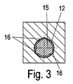
各プラグインダクトには、または図1のとくに好ましい実施形態では各接続デバイス4には、プラグイン部品として作製されたマーキングデバイスMがさらに接続されている。プラグイン部品の正確な形状は図3と併せて図1を参照することにより明瞭になる。従って、各プラグイン部品は頭部14とシャフト15とからなる。シャフト15はシリンダ状に形成されており、一方、頭部14は、この例示の実施形態では正方形状になっている。
An
This actuator part has a plug-in duct, in particular the plug-in
Further connected to each plug-in duct or to each connecting device 4 in the particularly preferred embodiment of FIG. 1 is a marking device M made as a plug-in part. The exact shape of the plug-in part will be clarified by referring to FIG. 1 in conjunction with FIG. Accordingly, each plug-in component includes a
とくに図3から明らかなように、プラグイン部品Mのシャフト15には、この場合長手方向に沿って延びている3つの安全ピン16が設けられている。それによって、シャフト15の基本的な直径はプラグインダクト13の直径未満である。このようにして、各プラグイン部品Mをプラグインダクト13の中へある力で挿入することができる。このプロセスでは、合成物質の形状弾性および材料弾性の特性が用いられるので、各プラグイン部品Fは形状により係止されて固定される(form−locking fixation)。この目的のために、各プラグインダクト13の接続のために自由空間17が設けられる。
As can be seen in particular in FIG. 3, the
図1には、プラグイン部品M、または各プラグイン部品Mの頭部14のハウジング10に向いている側面が少なくとも1つの成形ピン18を有し、この成形ピン18の断面が好ましくは台形であることが示されている。組み立てられた状態では、これらの成形ピン18は、頭部14に面しているアクチュエータ部品12の側面に対応して形成された凹部19に係合する。
従って、組み立て時、位置調整および心出しが行われ、また、簡単な手段で、頭部14とアクチュエータ部品との間の位置および回転について安全性がさらに確かめられることになる。また、各プラグイン部品Mを取り出す目的でこの領域にツールを差し込むことも考えられる。好ましくは、プラグイン方向Xに対して直交する面内の頭部14の表面は、レタリング用に大きな表面が利用可能となるように、また、取り出しが容易となるように、アクチュエータ部品12の対応する側面の表面よりも大きくなっている。
各プラグイン部品Mのシャフト15に長手方向に沿って延びるピン16を設け、各プラグインダクト13の下方に自由空間17を形成しているので、各プラグイン部品Mを形状により係止して固定する、すなわちアンダーカットのような作用により固定することができるという利点がある。さらに、プラグイン部品Mの各頭部14に成形ピン18を設けているので、位置調整および抜き出しが可能となるという利点がある。
In FIG. 1, the side of the plug-in part M or the
Thus, during assembly, position adjustment and centering are performed, and safety is further ascertained with simple means for position and rotation between the
Since a
ソケット基盤 1
プラグイン前側部 2
ソケット接触子 3
接続デバイス 4
摩擦バネ 5
摩擦ケージ 6
摩擦脚部 7
摩擦点 8
内壁 9
ハウジング 10
コンダクタプラグインダクト 11
アクチュエータ部品 12
プラグインダクト 13
頭部 14
シャフト 15
安全ストリップ 16
自由空間 17
成形ストリップ 18
成形ストリップ凹部 19
プラグイン方向 X
マーキングデバイス M
Socket base 1
Plug-in front side 2
Socket contact 3
Connected device 4
Friction spring 5
Friction cage 6
Friction point 8
Conductor plug-in
Plug-in
Molded
Molded
Plug-in direction X
Marking device M
Claims (15)
前記マーキングデバイス(M)が前記アクチュエータ部品(12)に配置されていることを特徴とする、接続デバイス。 A connecting part for fixing the electric conductor, in particular a friction spring, at least one actuator part (12), and at least a marking device (M) for displaying the symbol, such as a bus In the connection device (10) for connecting to
Connection device, characterized in that the marking device (M) is arranged on the actuator part (12).
Applications Claiming Priority (3)
| Application Number | Priority Date | Filing Date | Title |
|---|---|---|---|
| DE202011000748.0 | 2011-03-31 | ||
| DE201120000748 DE202011000748U1 (en) | 2011-03-31 | 2011-03-31 | Connection device for an electrical conductor with a marking device |
| PCT/EP2012/054647 WO2012130635A1 (en) | 2011-03-31 | 2012-03-16 | Connection device for an electrical conductor having a marking device |
Publications (2)
| Publication Number | Publication Date |
|---|---|
| JP2014514695A true JP2014514695A (en) | 2014-06-19 |
| JP2014514695A5 JP2014514695A5 (en) | 2015-03-05 |
Family
ID=45992182
Family Applications (1)
| Application Number | Title | Priority Date | Filing Date |
|---|---|---|---|
| JP2014501525A Pending JP2014514695A (en) | 2011-03-31 | 2012-03-16 | Connecting device for electrical conductors with marking device |
Country Status (9)
| Country | Link |
|---|---|
| US (1) | US9093762B2 (en) |
| EP (1) | EP2692020B1 (en) |
| JP (1) | JP2014514695A (en) |
| KR (1) | KR20140016962A (en) |
| CN (1) | CN103460510B (en) |
| DE (1) | DE202011000748U1 (en) |
| MX (1) | MX2013011133A (en) |
| SG (1) | SG193511A1 (en) |
| WO (1) | WO2012130635A1 (en) |
Families Citing this family (11)
| Publication number | Priority date | Publication date | Assignee | Title |
|---|---|---|---|---|
| JP2013143749A (en) * | 2012-01-12 | 2013-07-22 | Toshiba Corp | Electronic apparatus and control method of electronic apparatus |
| DE102013111574B4 (en) * | 2013-10-21 | 2017-01-12 | Wago Verwaltungsgesellschaft Mbh | Spring terminal and connector |
| CN105529544B (en) * | 2014-10-16 | 2019-03-01 | 哈廷电子有限公司及两合公司 | Plug-in connector |
| DE102014115009B3 (en) * | 2014-10-16 | 2016-02-25 | Harting Electric Gmbh & Co. Kg | Connectors |
| US10151890B2 (en) * | 2015-03-18 | 2018-12-11 | Leviton Manufacturing Co., Inc. | Data communication port insert configurable with indicia to customize data communication station labeling and identification |
| DE102015105545A1 (en) * | 2015-04-10 | 2016-10-13 | Phoenix Contact Gmbh & Co. Kg | Rangierwabe |
| US9831593B1 (en) * | 2015-06-20 | 2017-11-28 | Shawn Tartaglia | Network jack node identification system |
| DE202015105393U1 (en) * | 2015-10-12 | 2017-01-13 | Weidmüller Interface GmbH & Co. KG | Connecting device with a receptacle for a plug-in means |
| DE102017130389A1 (en) * | 2017-12-18 | 2019-06-19 | KL UG (haftungsbeschränkt) | Device for making an electrical connection |
| US10122100B1 (en) | 2018-03-16 | 2018-11-06 | Lee Reeves | Terminal block assemblies |
| TWI677149B (en) * | 2018-09-13 | 2019-11-11 | 進聯工業股份有限公司 | Improved structure of the connector |
Citations (6)
| Publication number | Priority date | Publication date | Assignee | Title |
|---|---|---|---|---|
| JPH0428178A (en) * | 1990-05-23 | 1992-01-30 | Fujitsu Ltd | Connector terminal structure |
| JPH08148205A (en) * | 1994-11-22 | 1996-06-07 | Amp Japan Ltd | Printed board terminal |
| US5741153A (en) * | 1995-07-27 | 1998-04-21 | Ortronics, Inc. | Modular connectors including terminated rear connector designation for insulation displacement connectors |
| JP3324995B2 (en) * | 1999-04-07 | 2002-09-17 | タイコエレクトロニクスアンプ株式会社 | Electrical connector |
| US20030194918A1 (en) * | 2002-04-12 | 2003-10-16 | Weidmuller Interface Gmbh & Co. | Electrical conductor connecting means |
| JP2009146738A (en) * | 2007-12-14 | 2009-07-02 | Ngk Spark Plug Co Ltd | Board connector, circuit board with connector, and board storage case |
Family Cites Families (14)
| Publication number | Priority date | Publication date | Assignee | Title |
|---|---|---|---|---|
| DE58773C (en) | ph. WIENER und j. R. schmitt in Bingen a. Rh | Cigar wrapping machine | ||
| DE967983C (en) * | 1952-08-17 | 1958-01-02 | Wago Klemmenwerk G M B H | Single or multi-pole terminal, embedded in a molded piece of insulating material, safe to touch, for screwless connection of electrical conductors |
| US3231847A (en) * | 1963-06-17 | 1966-01-25 | Emanuel J Kressel | Terminal block with removable marker strip |
| DE2416231C3 (en) * | 1974-04-03 | 1982-04-15 | Phönix Elektrizitätsgesellschaft H. Knümann GmbH & Co KG, 4933 Blomberg | Electrical connection terminal for connecting electrical conductors to a conductor rail carrying zero or ground potential |
| EP0352347A1 (en) * | 1988-07-27 | 1990-01-31 | C.A. Weidmüller GmbH & Co. | Electrical connector |
| JP2000048874A (en) * | 1998-07-30 | 2000-02-18 | Osada:Kk | Terminal box |
| DE20014918U1 (en) * | 1999-12-16 | 2001-05-23 | Weidmueller Interface | Connection element for connecting cable shields |
| DE20205821U1 (en) * | 2002-04-12 | 2003-08-21 | Weidmueller Interface | Connection device for an electrical conductor has spring contact within body |
| DE10237701B4 (en) * | 2002-08-16 | 2010-09-16 | Wago Verwaltungsgesellschaft Mbh | Connecting terminal for single, stranded, in particular finely stranded, electrical conductors |
| DE202004009980U1 (en) * | 2004-06-25 | 2005-11-03 | Weidmüller Interface GmbH & Co. KG | marking |
| EP2316150B1 (en) * | 2008-08-27 | 2013-04-24 | Phoenix Contact GmbH & Co. KG | Electrical terminal |
| DE202010008028U1 (en) | 2009-07-18 | 2010-12-30 | Weidmüller Interface GmbH & Co. KG | Connection device for conductors |
| DE102009050367A1 (en) * | 2009-10-22 | 2011-04-28 | Phoenix Contact Gmbh & Co. Kg | Spring clamp connection terminal |
| DE202011050120U1 (en) * | 2011-05-13 | 2012-08-30 | Weidmüller Interface GmbH & Co. KG | Clamping unit and connecting device with such a clamping unit |
-
2011
- 2011-03-31 DE DE201120000748 patent/DE202011000748U1/en not_active Expired - Lifetime
-
2012
- 2012-03-16 JP JP2014501525A patent/JP2014514695A/en active Pending
- 2012-03-16 SG SG2013070016A patent/SG193511A1/en unknown
- 2012-03-16 US US13/983,966 patent/US9093762B2/en not_active Expired - Fee Related
- 2012-03-16 KR KR20137028624A patent/KR20140016962A/en not_active Application Discontinuation
- 2012-03-16 WO PCT/EP2012/054647 patent/WO2012130635A1/en active Application Filing
- 2012-03-16 CN CN201280017808.XA patent/CN103460510B/en not_active Expired - Fee Related
- 2012-03-16 EP EP12715610.7A patent/EP2692020B1/en not_active Not-in-force
- 2012-03-16 MX MX2013011133A patent/MX2013011133A/en active IP Right Grant
Patent Citations (6)
| Publication number | Priority date | Publication date | Assignee | Title |
|---|---|---|---|---|
| JPH0428178A (en) * | 1990-05-23 | 1992-01-30 | Fujitsu Ltd | Connector terminal structure |
| JPH08148205A (en) * | 1994-11-22 | 1996-06-07 | Amp Japan Ltd | Printed board terminal |
| US5741153A (en) * | 1995-07-27 | 1998-04-21 | Ortronics, Inc. | Modular connectors including terminated rear connector designation for insulation displacement connectors |
| JP3324995B2 (en) * | 1999-04-07 | 2002-09-17 | タイコエレクトロニクスアンプ株式会社 | Electrical connector |
| US20030194918A1 (en) * | 2002-04-12 | 2003-10-16 | Weidmuller Interface Gmbh & Co. | Electrical conductor connecting means |
| JP2009146738A (en) * | 2007-12-14 | 2009-07-02 | Ngk Spark Plug Co Ltd | Board connector, circuit board with connector, and board storage case |
Also Published As
| Publication number | Publication date |
|---|---|
| WO2012130635A1 (en) | 2012-10-04 |
| EP2692020B1 (en) | 2016-06-15 |
| DE202011000748U1 (en) | 2012-07-04 |
| US20140017934A1 (en) | 2014-01-16 |
| CN103460510B (en) | 2017-05-03 |
| US9093762B2 (en) | 2015-07-28 |
| SG193511A1 (en) | 2013-10-30 |
| CN103460510A (en) | 2013-12-18 |
| EP2692020A1 (en) | 2014-02-05 |
| KR20140016962A (en) | 2014-02-10 |
| MX2013011133A (en) | 2014-03-12 |
Similar Documents
| Publication | Publication Date | Title |
|---|---|---|
| JP2014514695A (en) | Connecting device for electrical conductors with marking device | |
| JP6272262B2 (en) | Card connector | |
| US20120156898A1 (en) | Connection Of Printed Circuit Boards | |
| JP2014514695A5 (en) | ||
| US20180331449A1 (en) | Contacting device for contacting an electrical conductor to an electrical conductor path | |
| EP2843765B1 (en) | Wire terminal structure | |
| US9806442B2 (en) | Plug connection device | |
| US9343828B2 (en) | Push button power poke home connector | |
| JP6749092B2 (en) | Connector with stabilizing member and assembling method | |
| US20180351271A1 (en) | Plug-in contact | |
| ES2354464T3 (en) | CONNECTION CONTACT FOR ELECTRICAL CONDUCTORS. | |
| EP3136512A1 (en) | Connector | |
| US9793652B2 (en) | Contact device for contacting an electric conductor and an electrical connector to an electrical conductor track | |
| WO2017047362A1 (en) | Probe pin and inspection tool using same | |
| US20080207035A1 (en) | Contacting Device for a Flexible Ribbon Conductor | |
| JP5203273B2 (en) | Plug-in equipment | |
| CN101454944B (en) | Electrical connection terminal comprising a terminal housing | |
| JP2013084476A5 (en) | ||
| JP2009146579A (en) | Connector | |
| CN204156163U (en) | A kind of electronic connector | |
| FR2910183B1 (en) | SECURE ELECTRICAL CONTACT | |
| CA2782050C (en) | Connection system for connecting a single-row housing to a terminal element | |
| KR101761347B1 (en) | Test socket | |
| JP6924679B2 (en) | Press-fitting method of press-fit terminal, electrical connector for board with press-fit terminal | |
| KR200414990Y1 (en) | The module type guide block of the socket for testing memory module |
Legal Events
| Date | Code | Title | Description |
|---|---|---|---|
| A521 | Request for written amendment filed |
Free format text: JAPANESE INTERMEDIATE CODE: A523 Effective date: 20150109 |
|
| A621 | Written request for application examination |
Free format text: JAPANESE INTERMEDIATE CODE: A621 Effective date: 20150109 |
|
| A977 | Report on retrieval |
Free format text: JAPANESE INTERMEDIATE CODE: A971007 Effective date: 20150716 |
|
| A131 | Notification of reasons for refusal |
Free format text: JAPANESE INTERMEDIATE CODE: A131 Effective date: 20150721 |
|
| A601 | Written request for extension of time |
Free format text: JAPANESE INTERMEDIATE CODE: A601 Effective date: 20151013 |
|
| A521 | Request for written amendment filed |
Free format text: JAPANESE INTERMEDIATE CODE: A523 Effective date: 20151222 |
|
| A02 | Decision of refusal |
Free format text: JAPANESE INTERMEDIATE CODE: A02 Effective date: 20160126 |
|
| A521 | Request for written amendment filed |
Free format text: JAPANESE INTERMEDIATE CODE: A523 Effective date: 20160519 |