JP2014206564A - Imaging apparatus and control method therefor - Google Patents
Imaging apparatus and control method therefor Download PDFInfo
- Publication number
- JP2014206564A JP2014206564A JP2013082499A JP2013082499A JP2014206564A JP 2014206564 A JP2014206564 A JP 2014206564A JP 2013082499 A JP2013082499 A JP 2013082499A JP 2013082499 A JP2013082499 A JP 2013082499A JP 2014206564 A JP2014206564 A JP 2014206564A
- Authority
- JP
- Japan
- Prior art keywords
- image
- photoelectric conversion
- image signal
- conversion unit
- output
- Prior art date
- Legal status (The legal status is an assumption and is not a legal conclusion. Google has not performed a legal analysis and makes no representation as to the accuracy of the status listed.)
- Granted
Links
- 238000003384 imaging method Methods 0.000 title claims abstract description 26
- 238000000034 method Methods 0.000 title claims description 21
- 238000006243 chemical reaction Methods 0.000 claims abstract description 75
- 230000003287 optical effect Effects 0.000 claims abstract description 45
- 238000001514 detection method Methods 0.000 claims abstract description 32
- 210000001747 pupil Anatomy 0.000 claims abstract description 24
- 229920006395 saturated elastomer Polymers 0.000 abstract description 6
- 230000008569 process Effects 0.000 description 11
- 238000010586 diagram Methods 0.000 description 8
- 230000006870 function Effects 0.000 description 5
- 230000007423 decrease Effects 0.000 description 4
- 238000012545 processing Methods 0.000 description 4
- 108010076504 Protein Sorting Signals Proteins 0.000 description 3
- 230000004907 flux Effects 0.000 description 3
- 230000004075 alteration Effects 0.000 description 2
- 230000008859 change Effects 0.000 description 2
- 239000003086 colorant Substances 0.000 description 2
- 230000002093 peripheral effect Effects 0.000 description 2
- 238000004891 communication Methods 0.000 description 1
- 230000006835 compression Effects 0.000 description 1
- 238000007906 compression Methods 0.000 description 1
- 238000012790 confirmation Methods 0.000 description 1
- 238000013461 design Methods 0.000 description 1
Images


Classifications
-
- H—ELECTRICITY
- H04—ELECTRIC COMMUNICATION TECHNIQUE
- H04N—PICTORIAL COMMUNICATION, e.g. TELEVISION
- H04N23/00—Cameras or camera modules comprising electronic image sensors; Control thereof
- H04N23/60—Control of cameras or camera modules
- H04N23/67—Focus control based on electronic image sensor signals
-
- G—PHYSICS
- G06—COMPUTING; CALCULATING OR COUNTING
- G06T—IMAGE DATA PROCESSING OR GENERATION, IN GENERAL
- G06T5/00—Image enhancement or restoration
- G06T5/50—Image enhancement or restoration by the use of more than one image, e.g. averaging, subtraction
-
- H—ELECTRICITY
- H01—ELECTRIC ELEMENTS
- H01L—SEMICONDUCTOR DEVICES NOT COVERED BY CLASS H10
- H01L27/00—Devices consisting of a plurality of semiconductor or other solid-state components formed in or on a common substrate
- H01L27/14—Devices consisting of a plurality of semiconductor or other solid-state components formed in or on a common substrate including semiconductor components sensitive to infrared radiation, light, electromagnetic radiation of shorter wavelength or corpuscular radiation and specially adapted either for the conversion of the energy of such radiation into electrical energy or for the control of electrical energy by such radiation
- H01L27/144—Devices controlled by radiation
- H01L27/146—Imager structures
-
- H—ELECTRICITY
- H04—ELECTRIC COMMUNICATION TECHNIQUE
- H04N—PICTORIAL COMMUNICATION, e.g. TELEVISION
- H04N23/00—Cameras or camera modules comprising electronic image sensors; Control thereof
- H04N23/10—Cameras or camera modules comprising electronic image sensors; Control thereof for generating image signals from different wavelengths
- H04N23/12—Cameras or camera modules comprising electronic image sensors; Control thereof for generating image signals from different wavelengths with one sensor only
-
- H—ELECTRICITY
- H04—ELECTRIC COMMUNICATION TECHNIQUE
- H04N—PICTORIAL COMMUNICATION, e.g. TELEVISION
- H04N23/00—Cameras or camera modules comprising electronic image sensors; Control thereof
- H04N23/60—Control of cameras or camera modules
- H04N23/67—Focus control based on electronic image sensor signals
- H04N23/672—Focus control based on electronic image sensor signals based on the phase difference signals
-
- H—ELECTRICITY
- H04—ELECTRIC COMMUNICATION TECHNIQUE
- H04N—PICTORIAL COMMUNICATION, e.g. TELEVISION
- H04N23/00—Cameras or camera modules comprising electronic image sensors; Control thereof
- H04N23/80—Camera processing pipelines; Components thereof
- H04N23/84—Camera processing pipelines; Components thereof for processing colour signals
-
- H—ELECTRICITY
- H04—ELECTRIC COMMUNICATION TECHNIQUE
- H04N—PICTORIAL COMMUNICATION, e.g. TELEVISION
- H04N25/00—Circuitry of solid-state image sensors [SSIS]; Control thereof
- H04N25/10—Circuitry of solid-state image sensors [SSIS]; Control thereof for transforming different wavelengths into image signals
- H04N25/11—Arrangement of colour filter arrays [CFA]; Filter mosaics
- H04N25/13—Arrangement of colour filter arrays [CFA]; Filter mosaics characterised by the spectral characteristics of the filter elements
- H04N25/134—Arrangement of colour filter arrays [CFA]; Filter mosaics characterised by the spectral characteristics of the filter elements based on three different wavelength filter elements
-
- H—ELECTRICITY
- H04—ELECTRIC COMMUNICATION TECHNIQUE
- H04N—PICTORIAL COMMUNICATION, e.g. TELEVISION
- H04N25/00—Circuitry of solid-state image sensors [SSIS]; Control thereof
- H04N25/70—SSIS architectures; Circuits associated therewith
- H04N25/703—SSIS architectures incorporating pixels for producing signals other than image signals
- H04N25/704—Pixels specially adapted for focusing, e.g. phase difference pixel sets
-
- H—ELECTRICITY
- H04—ELECTRIC COMMUNICATION TECHNIQUE
- H04N—PICTORIAL COMMUNICATION, e.g. TELEVISION
- H04N25/00—Circuitry of solid-state image sensors [SSIS]; Control thereof
- H04N25/70—SSIS architectures; Circuits associated therewith
- H04N25/71—Charge-coupled device [CCD] sensors; Charge-transfer registers specially adapted for CCD sensors
- H04N25/75—Circuitry for providing, modifying or processing image signals from the pixel array
-
- H—ELECTRICITY
- H04—ELECTRIC COMMUNICATION TECHNIQUE
- H04N—PICTORIAL COMMUNICATION, e.g. TELEVISION
- H04N9/00—Details of colour television systems
- H04N9/64—Circuits for processing colour signals
-
- H—ELECTRICITY
- H04—ELECTRIC COMMUNICATION TECHNIQUE
- H04N—PICTORIAL COMMUNICATION, e.g. TELEVISION
- H04N9/00—Details of colour television systems
- H04N9/64—Circuits for processing colour signals
- H04N9/68—Circuits for processing colour signals for controlling the amplitude of colour signals, e.g. automatic chroma control circuits
-
- G—PHYSICS
- G06—COMPUTING; CALCULATING OR COUNTING
- G06T—IMAGE DATA PROCESSING OR GENERATION, IN GENERAL
- G06T2207/00—Indexing scheme for image analysis or image enhancement
- G06T2207/10—Image acquisition modality
- G06T2207/10024—Color image
-
- G—PHYSICS
- G06—COMPUTING; CALCULATING OR COUNTING
- G06T—IMAGE DATA PROCESSING OR GENERATION, IN GENERAL
- G06T2207/00—Indexing scheme for image analysis or image enhancement
- G06T2207/20—Special algorithmic details
- G06T2207/20212—Image combination
- G06T2207/20224—Image subtraction
-
- H—ELECTRICITY
- H04—ELECTRIC COMMUNICATION TECHNIQUE
- H04N—PICTORIAL COMMUNICATION, e.g. TELEVISION
- H04N23/00—Cameras or camera modules comprising electronic image sensors; Control thereof
- H04N23/80—Camera processing pipelines; Components thereof
- H04N23/81—Camera processing pipelines; Components thereof for suppressing or minimising disturbance in the image signal generation
-
- H—ELECTRICITY
- H04—ELECTRIC COMMUNICATION TECHNIQUE
- H04N—PICTORIAL COMMUNICATION, e.g. TELEVISION
- H04N25/00—Circuitry of solid-state image sensors [SSIS]; Control thereof
- H04N25/70—SSIS architectures; Circuits associated therewith
- H04N25/702—SSIS architectures characterised by non-identical, non-equidistant or non-planar pixel layout
Abstract
Description
本発明はオートフォーカス機能を有する撮像装置に関する。 The present invention relates to an imaging apparatus having an autofocus function.
撮影光学系と撮像素子を有した撮像装置において、位相差式の焦点検出方法を用いて高速・高精度な焦点検出を行なう技術が従来より知られている。位相差式焦点検出技術においては、撮影光学系の射出光束を瞳分割手段により少なくとも2つの領域に分割し、各領域の光束を光電変換して1対2像の焦点検出用信号列を得る。そしてその2つの信号列の相対的像ずれ量から、予定焦点面の焦点ずれ量、いわゆるデフォーカス量を検出する。ここで、位相差式の焦点検出においては、合焦時には2像の信号列の強度は一致し、上記の相対的像ずれ量もゼロになるはずである。しかしながら、焦点検出光束の撮影光学系によるケラレや、撮影光学系の諸収差により、2像の一致度が低下し、焦点検出誤差を生ずる。また、上記のケラレや諸収差により、2像の相対的横ずれ量とデフォーカス量の比例関係も崩れる。従って、高精度な焦点検出を行なうためには、これらの誤差の解消が必要であり、その技術も提案されている。 2. Description of the Related Art Conventionally, a technique for performing high-speed and high-precision focus detection using a phase difference type focus detection method in an image pickup apparatus having a photographing optical system and an image sensor has been known. In the phase difference type focus detection technique, the exit light flux of the photographing optical system is divided into at least two areas by the pupil dividing means, and the light flux in each area is photoelectrically converted to obtain a focus detection signal sequence of one-to-two images. Then, the defocus amount of the planned focal plane, so-called defocus amount, is detected from the relative image shift amounts of the two signal sequences. Here, in the phase difference type focus detection, the intensities of the signal sequences of the two images coincide with each other at the time of focusing, and the relative image shift amount should be zero. However, the degree of coincidence of the two images decreases due to vignetting of the focus detection light beam by the photographing optical system and various aberrations of the photographing optical system, resulting in a focus detection error. In addition, the proportional relationship between the amount of relative lateral shift between the two images and the amount of defocus is lost due to the above-described vignetting and various aberrations. Therefore, in order to perform highly accurate focus detection, it is necessary to eliminate these errors, and a technique for this has been proposed.
一方で、撮像素子として2次元CMOSセンサ等を用いて、センサ上に位相差検出のための焦点検出用画素を配置する技術も提案されている。撮像用画素と焦点検出用画素は同一平面上に配置されているため、撮像用画素が合焦状態にある時は、焦点検出用画素も合焦状態にある。したがって、合焦時には位相差検出のための2像には相対的な像ずれは原理上発生せず、誤差が発生しにくい。しかしながら、焦点検出用画素には2つの光電変換部が存在するため、蓄積された画素の信号を読み出す回路が複雑になる。そこで画素信号を読み出す回路の複雑化を抑制する方法が特許文献1に記載されている。 On the other hand, a technique has been proposed in which a focus detection pixel for phase difference detection is arranged on a sensor using a two-dimensional CMOS sensor or the like as an image sensor. Since the imaging pixel and the focus detection pixel are arranged on the same plane, when the imaging pixel is in focus, the focus detection pixel is also in focus. Therefore, relative image shift does not occur in principle between the two images for phase difference detection during focusing, and errors are unlikely to occur. However, since there are two photoelectric conversion units in the focus detection pixel, a circuit for reading out accumulated pixel signals becomes complicated. Therefore, Patent Document 1 discloses a method for suppressing the complexity of a circuit for reading out pixel signals.
特許文献1に記載された技術においては、2つの光電変換部を有する複数の焦点検出用画素について、2つの光電変換部の出力信号同士を加算した信号を焦点検出用画素から出力する。 In the technique described in Patent Document 1, for a plurality of focus detection pixels having two photoelectric conversion units, a signal obtained by adding the output signals of the two photoelectric conversion units to each other is output from the focus detection pixel.
しかしながら、特許文献1では焦点検出用画素が出力できる値を超えた場合(飽和した場合)には、焦点検出用画素の2つの光電変換部の間で電荷漏れによるクロストークが生じる。クロストークにより、出力信号に撮影光学系の射出光束を光電変換した信号以外の信号が含まれることになり、焦点検出を正確に行うことができない。 However, in Patent Document 1, when the value that can be output by the focus detection pixel is exceeded (saturated), crosstalk due to charge leakage occurs between the two photoelectric conversion units of the focus detection pixel. Due to the crosstalk, the output signal includes a signal other than the signal obtained by photoelectrically converting the light beam emitted from the photographing optical system, and focus detection cannot be performed accurately.
本発明は上述した課題に鑑みてなされたものであり、その目的は、位相差検出可能な撮像素子を有する撮像装置において、飽和する画素があっても焦点検出不能となることを抑制することである。 The present invention has been made in view of the above-described problems, and an object of the present invention is to suppress an inability to detect a focus even if there is a saturated pixel in an imaging apparatus having an imaging element capable of detecting a phase difference. is there.
本発明に係わる撮像装置は、撮影光学系の一部の瞳領域を通過した光を受光する第1の光電変換部と、前記撮影光学系の前記一部の瞳領域とは異なる瞳領域を通過した光を受光する第2の光電変換部の少なくとも2つの光電変換部と、所定の色の色フィルタとをそれぞれ有する複数の画素を備える撮像素子と、前記撮像素子から、前記第1の光電変換部から得られる第1の像信号と、前記第1の光電変換部から得られる第1の像信号と前記第2の光電変換部から得られる第2の像信号とを加算した加算信号とを読み出す読み出し手段と、前記加算信号から前記第1の像信号を差し引くことにより前記第2の像信号を得る減算手段と、前記第1の像信号と前記第2の像信号とに基づいて前記撮影光学系の焦点状態を検出する焦点検出手段と、前記第1の光電変換部の出力と、前記第2の光電変換部の出力が所定の閾値を超えないように抑制するリミッタ手段と、を備え、前記リミッタ手段は、前記第1の像信号と第2の像信号に対して、異なる色フィルタについての前記第1の光電変換部の出力と、前記第2の光電変換部の出力が所定の閾値を超えないように抑制することを特徴とする。 An imaging apparatus according to the present invention passes through a first photoelectric conversion unit that receives light that has passed through a part of the pupil region of the photographing optical system, and a pupil region that is different from the part of the pupil region of the photographing optical system. An image sensor comprising a plurality of pixels each having at least two photoelectric converters of a second photoelectric converter that receives the emitted light, and a color filter of a predetermined color, and the first photoelectric converter from the image sensor A first image signal obtained from the first photoelectric conversion unit, and an addition signal obtained by adding the first image signal obtained from the first photoelectric conversion unit and the second image signal obtained from the second photoelectric conversion unit. Read-out means for reading out, subtracting means for obtaining the second image signal by subtracting the first image signal from the addition signal, and the photographing based on the first image signal and the second image signal A focus detection means for detecting the focus state of the optical system; Limiter means for suppressing the output of the first photoelectric conversion unit and the output of the second photoelectric conversion unit from exceeding a predetermined threshold, and the limiter means includes the first image signal and the first image signal. It is characterized in that the output of the first photoelectric conversion unit and the output of the second photoelectric conversion unit for different color filters are suppressed so as not to exceed a predetermined threshold for two image signals.
本発明によれば、位相差検出可能な撮像素子を有する撮像装置において、飽和する画素があっても焦点検出不能となることを抑制することが可能となる。 According to the present invention, in an imaging apparatus having an imaging element capable of detecting a phase difference, it is possible to suppress the focus detection from becoming impossible even if there are saturated pixels.
以下、本発明の一実施形態について、添付図面を参照して詳細に説明する。 Hereinafter, an embodiment of the present invention will be described in detail with reference to the accompanying drawings.
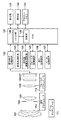
図1は本発明に係る撮像装置の一実施形態の構成図で、撮像素子を有したカメラ本体と撮影光学系が一体となった電子カメラを示しており、動画及び静止画が記録可能である。図1において、101は被写体像を結像させる撮影光学系の先端に配置された第1レンズ群で、光軸方向に移動可能に保持される。102は絞りで、その開口径を調節することで撮影時の光量調節を行なうほか、静止画撮影時には露光秒時調節用シャッタとしても機能する。103は第2レンズ群である。そして、絞り102及び第2レンズ群103は一体となって光軸方向に駆動され、第1レンズ群101の移動動作との連動により、変倍作用(ズーム機能)をなす。105は第3レンズ群で、光軸方向の移動により、焦点調節を行なう。106は光学的ローパスフィルタで、撮影画像の偽色やモアレを軽減するための光学素子である。
FIG. 1 is a configuration diagram of an embodiment of an imaging apparatus according to the present invention, showing an electronic camera in which a camera body having an imaging element and a photographing optical system are integrated, and can record moving images and still images. . In FIG. 1,
107は焦点検出可能な画素を有する撮像素子で、CMOSセンサとその周辺回路で構成される。撮像素子107には、横方向にM画素、縦方向にN画素の受光ピクセルが正方配置され、ベイヤー配列の原色カラーモザイクフィルタがオンチップで形成された、2次元単板カラーセンサが用いられる。撮像素子107は各画素に複数の光電変換部を有し、各々の画素には色フィルタが配置されている。 Reference numeral 107 denotes an image sensor having a pixel capable of focus detection, and is composed of a CMOS sensor and its peripheral circuits. The image sensor 107 is a two-dimensional single-plate color sensor in which M pixels in the horizontal direction and N pixels in the vertical direction are squarely arranged, and a primary color mosaic filter in a Bayer array is formed on-chip. The image sensor 107 has a plurality of photoelectric conversion units in each pixel, and a color filter is arranged in each pixel.
111はズームアクチュエータで、不図示のカム筒を手動もしくはアクチュエータで回動することにより、第1レンズ群101ないし第3レンズ群105を光軸方向に駆動し、変倍操作を行なう。112は絞りアクチュエータで、絞り102の開口径を制御して撮影光量を調節すると共に、静止画撮影時の露光時間制御を行なう。114はフォーカスアクチュエータで、第3レンズ群105を光軸方向に駆動して焦点調節を行なう。
121はCPUで、カメラ本体の種々の制御を司るために、演算部、ROM、RAM、A/Dコンバータ、D/Aコンバータ、通信インターフェイス回路等を有する。そしてROMに記憶された所定のプログラムに基づいて、カメラが有する各種回路を駆動し、焦点調節(AF)、撮影、画像処理、記録等の一連の動作を実行する。
122は撮像素子駆動回路で、撮像素子107の撮像動作を制御するとともに、取得した画像信号をA/D変換してCPU121に送信する。123は画像処理回路で、撮像素子107が取得した画像のカラー補間、γ変換、画像圧縮等の処理を行なう。124は焦点検出手段としての位相差演算処理回路で、撮像素子107の各画素の2つの光電変換領域から得られる信号をAF用A像信号とAF用B像信号として、A像とB像の像ずれ量を相関演算で求め、ピントずれ量(焦点状態)を算出する回路である。125はフォーカス駆動回路で、焦点検出結果に基づいてフォーカスアクチュエータ114を駆動制御し、第3レンズ群105を光軸方向に駆動して焦点調節を行なう。126は絞り駆動回路で、絞りアクチュエータ112を駆動制御して絞り102の開口を制御する。127はズーム駆動回路で、撮影者のズーム操作に応じてズームアクチュエータ111を駆動する。
128はリミッタ部でA像信号とB像信号の加算信号が所定の閾値を超えることを抑制する。129は制御部でリミッタ部128においてA像信号とB像信号の加算信号が所定の閾値を超える場合にはリミッタ部を制御することで、A像とA+B像を生成する。
131はLCD等の表示部で、カメラの撮影モードに関する情報、撮影時のプレビュー画像と撮影後の確認用画像、焦点検出時の合焦状態表示画像を表示する。132は操作部で、電源スイッチ、撮影開始スイッチ、ズーム操作スイッチ、撮影モード選択スイッチ等で構成される。133は着脱可能なフラッシュメモリで、動画及び静止画を含む撮影済み画像を記録する。
図2は本発明の一実施形態における撮像素子107の画素配列を示した図で、2次元CMOSエリアセンサの縦(Y方向)6行と横(X方向)8列の範囲を、撮影光学系側から観察した状態を示している。色フィルタはベイヤー配列が適用され、奇数行の画素には、左から順に緑(Green)と赤(Red)の色フィルタが画素に対応して交互に設けられる。また、偶数行の画素には、左から順に青(Blue)と緑(Green)の色フィルタが画素に対応して交互に設けられる。円211iはオンチップマイクロレンズを表わす。オンチップマイクロレンズの内側に配置された複数の矩形はそれぞれ光電変換部であり、撮影光学系の一部の瞳領域を通過した光を受光する第1の光電変換部211aと、撮影光学系の別の瞳領域を通過した光を受光する第2の光電変換部211bに分けられる。
FIG. 2 is a diagram showing a pixel arrangement of the image sensor 107 according to an embodiment of the present invention. The range of the vertical (Y direction) 6 rows and the horizontal (X direction) 8 columns of the two-dimensional CMOS area sensor is shown in FIG. The state observed from the side is shown. A Bayer arrangement is applied to the color filters, and green (Red) and red (Red) color filters are alternately provided corresponding to the pixels in the odd-numbered rows in order from the left. In addition, blue (Blue) and green (Green) color filters are alternately provided corresponding to the pixels in the even-numbered rows in order from the left. A
本実施形態では、すべての画素の光電変換部はX方向に2分割され、分割された各々の領域の光電変換信号は、第1の光電変換部211aの信号は色フィルタごとに独立して読み出せるが、第2の光電変換部211bの信号は独立して読み出すことができない。第2の光電変換部211bの信号は、第1と第2の光電変化部の出力を加算後に読み出した信号から第1の光電変換部211aの信号を減算することで算出する。
In the present embodiment, the photoelectric conversion units of all the pixels are divided into two in the X direction, and the photoelectric conversion signal of each divided region is read independently from the signal of the first
そして、第1の光電変換部211aと第2の光電変換部211bからの信号は、後述する方法で位相差式焦点検出に用いられるほか、視差情報を有した複数画像から構成される3D(3−Dimensional)画像を生成するのに用いることもできる。一方で、分割された光電変換部の出力を加算した情報は、通常の撮影画像として用いられる。
The signals from the first
ここで、位相差式焦点検出を行なう場合の画素信号について説明する。本実施形態においては、図2のマイクロレンズ211iと、分割された光電変換部211a及び211bで、撮影光学系の射出光束を瞳分割する。そして、同一行上に配置された所定範囲内の複数の画素211において、光電変換部211aの出力をつなぎ合わせて編成したものを第1の像であるA像、同じく光電変換部211bの出力をつなぎ合わせて編成したものを第2の像であるB像とする。このように生成した第1の像であるA像と第2の像であるB像の相対的な像ずれ量を相関演算により検出することで、所定領域の焦点ずれ量、すなわちデフォーカス量を検出することができる。
Here, a pixel signal in the case of performing phase difference focus detection will be described. In this embodiment, the
図3は本実施形態の撮像素子107における読み出し回路の構成を示した図である。151は水平走査回路、153は垂直走査回路である。そして各画素の境界部には、水平走査ライン152a及び152bと、垂直走査ライン154a及び154bが配線され、各光電変換部はこれらの走査ラインを介して信号が外部に読み出される。
FIG. 3 is a diagram showing a configuration of a readout circuit in the image sensor 107 of the present embodiment.
なお、本実施形態の撮像素子107は以下の2種類の読み出しモードを有する。第1の読み出しモードは全画素読み出しモードと称するもので、高精細静止画を撮像するためのモードである。この場合は、全画素の信号が読み出される。第2の読み出しモードは間引き読み出しモードと称するもので、動画記録、もしくはプレビュー画像の表示のみを行なうためのモードである。この場合に必要な画素数は全画素よりも少ないため、画素群はX方向及びY方向ともに所定比率に間引いた画素のみ読み出す。 Note that the image sensor 107 of the present embodiment has the following two types of readout modes. The first readout mode is called an all-pixel readout mode and is a mode for capturing a high-definition still image. In this case, signals of all pixels are read out. The second readout mode is called a thinning readout mode, and is a mode for performing only moving image recording or preview image display. In this case, since the number of necessary pixels is smaller than that of all the pixels, the pixel group reads out only the pixels thinned out at a predetermined ratio in both the X direction and the Y direction.
通常の撮像用画像では(A+B)像を読み出せば良いが、複数の測距領域で位相差検出を行う場合にはA像信号とB像信号を読み出して、A像とB像の像ずれ量を相関演算により検出することで、デフォーカス量を算出する。 (A + B) image may be read out for a normal imaging image, but when phase difference detection is performed in a plurality of ranging areas, the A image signal and the B image signal are read and the image shift between the A image and the B image is detected. The defocus amount is calculated by detecting the amount by correlation calculation.
図4は本実施形態の撮像装置において、撮影光学系の射出瞳面と、像高0すなわち像面中央近傍に配置された撮像素子107の光電変換部の共役関係を説明する図である。撮像素子内の光電変換部211a,211bと撮影光学系の射出瞳面は、オンチップマイクロレンズによって共役関係となるように設計される。そして撮影光学系の射出瞳は、一般的に光量調節用の虹彩絞りが置かれる面とほぼ一致する。一方、本実施形態の撮影光学系は変倍機能を有したズームレンズであるが、光学タイプによっては変倍操作を行なうと、射出瞳の像面からの距離や大きさが変化する。図4における撮影光学系は、焦点距離が広角端と望遠端の中間、すなわちMiddleの状態を示している。この状態での射出瞳距離をZmidとし、これを標準的な射出瞳距離Znormと仮定して、オンチップマイクロレンズの形状設計がなされる。
FIG. 4 is a diagram for explaining the conjugate relationship between the exit pupil plane of the photographic optical system and the photoelectric conversion unit of the image sensor 107 arranged near the
図4において、101は第1レンズ群、101bは第1レンズ群を保持する鏡筒部材、105は第3レンズ群、105bは第3レンズ群を保持する鏡筒部材である。102は絞りで、102aは絞り開放時の開口径を規定する開口板、102bは絞り込み時の開口径を調節するための絞り羽根である。なお、撮影光学系を通過する光束の制限部材として作用する101b,102a,102b,105bは、像面から観察した場合の光学的な虚像を示している。また、絞り102の近傍における合成開口をレンズの射出瞳と定義し、前述したように像面からの距離をZmidとしている。
In FIG. 4, 101 is a first lens group, 101b is a lens barrel member that holds the first lens group, 105 is a third lens group, and 105b is a lens barrel member that holds the third lens group.
211は画素で、最下層より、211a及び211bの光電変換部、211e〜211gの配線層、色フィルタ211h、及びオンチップマイクロレンズ211iの各部材で構成される。光電変換部211a,211bはオンチップマイクロレンズ211iによって撮影光学系の射出瞳面に投影され、その投影像はEP1a,EP1bとなる。
ここで、絞り102が開放(例えばF2.8)の場合、撮影光学系を通過する光束の最外部をL(F2.8)で示すが、上記投影像EP1a,EP1bは絞り開口でけられることが無い。一方、絞り102が小絞り(例えばF5.6)の場合、撮影光学系を通過する光束の最外部をL(F5.6)で示すが、上記の投影像EP1a,EP1bの外側は絞り開口でけられる。ただし、像面中央では各投影像EP1a,EP1bのけられ状態は光軸に対して対称となり、各光電変換部211a,211bが受光する光量は等しい。
Here, when the
次に、本実施形態の光電変換部の出力値が上限値を超える(飽和した)場合の対策について説明する。各画素の光電変換部は撮影光学系を通過する光束から光量を受光し、光電変換することで光量に応じた信号を出力する。しかし、光量が多い高輝度被写体の場合には光電変換部211a,211bで蓄積できる光量の上限値を超えて隣接した光電変換部に対して電荷が漏れ、クロストークが生じてしまう。光電変換部211aから生成されるA像信号と光電変換部211bから生成されるB像信号間にクロストークがあるために、A像信号とB像信号の像ずれ量の誤差となる。そのため、像ずれ量を相関演算により検出したデフォーカス量に誤差が生じ、所望の被写体に合焦できない。
Next, a countermeasure when the output value of the photoelectric conversion unit of the present embodiment exceeds the upper limit value (saturates) will be described. The photoelectric conversion unit of each pixel receives a light amount from a light beam passing through the photographing optical system, and outputs a signal corresponding to the light amount by performing photoelectric conversion. However, in the case of a high-brightness subject with a large amount of light, charge leaks to adjacent photoelectric conversion units beyond the upper limit of the amount of light that can be accumulated by the
本実施形態ではB像信号を生成する過程において、(A+B)像信号からA像信号を減算することでB像信号を生成している。像信号には出力可能な上限値があり、本実施形態ではA、B、A+B像ともに同一の上限値となっている。A像が出力可能な上限値となった場合には、(A+B)像の出力信号も上限値となるため、A+B像の信号とA像の信号が同じく上限値となる。つまり、A像信号が上限値の場合にはA+B像も同一の上限値となり、B像信号は(A+B)像からA像を減算することで生成するため、出力が0となってしまう。この場合にはA像信号は上限値をとり、B像信号は0となるため、誤った像信号を生成していることになる。そのため、A像とB像の像ずれ量を相関演算により検出し、デフォーカス量を算出しても、所望の被写体に合焦させることはできない。さらにA像が上限値に達していない場合でも、A+B像で飽和している場合には、B像生成時に像信号が失われ、A像とB像の像ずれ量から相関演算によりデフォーカス量を算出しても、所望の被写体に合焦させることはできない。 In the present embodiment, in the process of generating the B image signal, the B image signal is generated by subtracting the A image signal from the (A + B) image signal. The image signal has an upper limit value that can be output. In this embodiment, the A, B, and A + B images have the same upper limit value. When the upper limit value at which the A image can be output is reached, the output signal of the (A + B) image also becomes the upper limit value, so that the A + B image signal and the A image signal have the same upper limit value. That is, when the A image signal is the upper limit value, the A + B image also has the same upper limit value, and the B image signal is generated by subtracting the A image from the (A + B) image, so the output becomes zero. In this case, the A image signal takes the upper limit value and the B image signal is 0, so that an erroneous image signal is generated. Therefore, even if the image shift amount between the A image and the B image is detected by correlation calculation and the defocus amount is calculated, the desired subject cannot be focused. Further, even when the A image does not reach the upper limit value, if it is saturated with the A + B image, the image signal is lost when the B image is generated, and the defocus amount is obtained by the correlation calculation from the image shift amounts of the A image and the B image. However, it is impossible to focus on a desired subject.
以上のように、高輝度被写体に対して各画素が飽和する場合でも合焦させるためにはA像、A+B像が共に上限値に達しないように像信号を制御しなければならない。そこで、本実施形態ではA像とB像が所定の閾値を超えることを抑制するリミッタ部128を設け、かつリミッタ部128を制御する制御部129を設けることで像信号が上限値に達しないように制御する。
As described above, the image signal must be controlled so that both the A image and the A + B image do not reach the upper limit value in order to achieve focusing even when each pixel is saturated with respect to the high brightness subject. Therefore, in the present embodiment, the
本実施形態では、A像信号は奇数行の緑(Green、以下G1)、赤(Red、以下R)、偶数行の青(Blue、以下B)、緑(Green、以下G2)の各色フィルタの画素を加算し輝度信号にするため、G1、R、B、G2の各色の段階で閾値を設ける。これによりG1、R、B、G2の特定の色が上限値に達した場合でも、リミッタ部128により閾値を設定し、制御部129で各像信号が閾値を超えることを抑制する。
In the present embodiment, the A image signal is an odd-numbered row of green (Green, hereinafter G1), red (Red, hereinafter R), even-numbered blue (Blue, hereinafter B), and green (Green, hereinafter G2) color filters. In order to add the pixels to obtain a luminance signal, a threshold value is provided at each color stage of G1, R, B, and G2. Thereby, even when specific colors of G1, R, B, and G2 reach the upper limit value, the
リミッタ部128はB像信号では、輝度信号に対して閾値を設定する。これは次のような理由による。B像をG1、R、B、G2ごとに生成するということは、A像とA+B像それぞれをG1、R、B、G2ごとに一旦記憶してから、B像のG1、R、B、G2を生成することになる。そのため、信号を記憶する回路や生成する回路等の規模が増大してしまう。そのためB像の信号はA像とA+B像の輝度信号から生成される。このことからリミット部128はB像信号では、閾値は輝度信号に対して設定し、制御部129で閾値を超えることを抑制する。
For the B image signal, the
次に本実施形態の各光電変換部の信号が上限値を超えないようにする飽和判定方法について図5〜図7を参照して説明する。図5は撮影光学系からの入射光量と撮像素子の出力信号を示しており、横軸に入射光量、縦軸に出力信号を示し、実線をA+B像、点線をA像、一点鎖線をB像としている。図6は合焦時の実信号の例であり、横軸に任意行の画素、縦軸に出力信号を示している。図7は本実施形態の動作を示すフローチャートである。 Next, a saturation determination method for preventing the signal of each photoelectric conversion unit of the present embodiment from exceeding the upper limit value will be described with reference to FIGS. FIG. 5 shows the amount of incident light from the imaging optical system and the output signal of the image sensor. The horizontal axis represents the incident light amount and the vertical axis represents the output signal. It is said. FIG. 6 is an example of a real signal at the time of focusing, and the horizontal axis indicates pixels in an arbitrary row, and the vertical axis indicates an output signal. FIG. 7 is a flowchart showing the operation of this embodiment.
飽和判定をしない場合を図5(a)、飽和判定する場合を図5(b)に示す。実信号の場合での飽和判定しない場合を図6(a)、飽和判定する場合を図6(b)に示す。図5(a)の入射光量が小さい0からA1の区間では、入射光量を光電変換しても各画素信号が上限値に達していないため(A1までの領域)、A像信号、B像信号ともに入射光量を反映した信号を出力できる。図5(a)の入射光量が大きいA1以上の区間になると、A+B像信号が上限値を超えてしまうことで、B像は(A+B)像からA像を減算することによって生成するため、B像自体の信号が減少してしまう。すなわち、本実施形態では、各像信号の上限値が同一の値のため、A像の信号が上限値の1/2を超えるときに、B像の信号がA像の影響により、減少していくことになる。つまり、A像の信号が1/2を超えるとB像信号はA像信号の影響により減少してしまう。つまり、本来A像信号の増加に対してB像信号も増加となるべきなのに、A像信号が上限値を超えることによって、A像信号の増加に対してB像信号が減少となり、逆の変化をしてしまう。これにより、図6(a)に示すようにA像とB像の像一致度が極端に低下してしまう。以上により、相関演算を行っても像一致度が低下しているために、算出したデフォーカス量が正確でなく、所望の被写体には合焦できない。 FIG. 5A shows the case where saturation determination is not performed, and FIG. 5B shows the case where saturation determination is performed. FIG. 6A shows a case where saturation determination is not performed in the case of an actual signal, and FIG. 6B shows a case where saturation determination is performed. In the interval from 0 to A1 where the incident light amount is small in FIG. 5A, each pixel signal does not reach the upper limit even if the incident light amount is photoelectrically converted (region up to A1), so the A image signal and the B image signal. Both can output a signal reflecting the amount of incident light. When the incident light amount in FIG. 5A is greater than or equal to A1, the A + B image signal exceeds the upper limit, and the B image is generated by subtracting the A image from the (A + B) image. The signal of the image itself is reduced. That is, in this embodiment, since the upper limit value of each image signal is the same value, when the A image signal exceeds 1/2 of the upper limit value, the B image signal decreases due to the influence of the A image. Will go. That is, if the A image signal exceeds 1/2, the B image signal is reduced due to the influence of the A image signal. That is, the B image signal should increase with respect to the increase in the A image signal, but if the A image signal exceeds the upper limit value, the B image signal decreases with respect to the increase in the A image signal, and the reverse change occurs. Will do. As a result, as shown in FIG. 6A, the image coincidence between the A image and the B image is extremely lowered. As described above, since the degree of image coincidence is reduced even if the correlation calculation is performed, the calculated defocus amount is not accurate and the desired subject cannot be focused.
次に飽和判定を行う場合について図5(b)を用いて説明する。図5(b)でもA像とB像の像信号が同一の値を取る場合を想定している。リミッタ部128はA像の像信号の出力が上限値の1/2となる値を閾値として設定し、制御部129で閾値を超えることを抑制する。これによりA像とB像がともに上限値の1/2以下となるため、A+B像が上限値になることはない。以上のように、飽和判定をすることによって図6(b)に示すように、合焦時のA像とB像の像一致度を低下させることなく、相関演算をすることができるので、正確なデフォーカス量が算出できる。
Next, a case where saturation determination is performed will be described with reference to FIG. FIG. 5B also assumes a case where the image signals of the A image and the B image take the same value. The
撮像素子の周辺部すなわち像高が大きな領域では、撮影光学系の口径食(ビグネッティング)により射出瞳径が小さくなる。それため画素の受光量が低下し、2つの光電変換部間で不均一となる。そして絞り開口径の減少とともに受光量の不均一性が顕著になる。以上から1画素にある2つの光電変換部211a,211bで受光量が異なる場合が存在する。そこで、2つの光電変換部211a,211bの信号であるA像信号とB像信号が同一の値ではない場合の飽和判定について図5(c)、5(d)、図6(c)、6(d)を用いて説明する。
In the peripheral portion of the image sensor, that is, in a region where the image height is large, the exit pupil diameter becomes small due to vignetting (vignetting) of the photographing optical system. As a result, the amount of light received by the pixel is reduced and nonuniform between the two photoelectric conversion units. As the aperture diameter of the diaphragm decreases, non-uniformity in the amount of received light becomes significant. From the above, there are cases where the received light amount differs between the two
A像の飽和判定はするがB像の飽和判定をしない場合が図5(c)、A像もB像も飽和判定をする場合を図5(d)に示す。図5(c)、5(d)では、A像信号よりB像信号が大きい場合を示している。A像信号が上限値の1/2以下の場合であっても、B像信号はすでに1/2を超える場合があるためA+B像の信号で上限値となる。B像信号はA+B像信号からA像信号を減算して生成するため、B像信号にA+B像信号が上限値を超えたことによる偽信号が出力されてしまう。これにより、図6(c)に示すようにA像とB像の像一致度が極端に低下してしまい、像ずれ量による相関演算から正確なデフォーカス量が算出できない。 FIG. 5C shows the case where the saturation determination of the A image is performed but the saturation determination of the B image is not performed, and FIG. 5D shows the case where the saturation determination is performed for both the A image and the B image. 5C and 5D show the case where the B image signal is larger than the A image signal. Even if the A image signal is less than or equal to ½ of the upper limit value, the B image signal may already exceed ½, so the A + B image signal becomes the upper limit value. Since the B image signal is generated by subtracting the A image signal from the A + B image signal, a false signal due to the A + B image signal exceeding the upper limit value is output to the B image signal. As a result, as shown in FIG. 6C, the image coincidence between the A image and the B image is extremely reduced, and an accurate defocus amount cannot be calculated from the correlation calculation based on the image shift amount.
本実施形態では図5(d)に示すようにB像信号にも閾値を設けている。具体的には、B像信号を上限値に対して1/2以下とする閾値を設けている。B像信号にも閾値を設けることでB像のみが上限値の1/2を超えることがないため、A像信号、B像信号のどちらかが1/2を超えてB像の信号にA+B像信号の飽和による偽信号が混入することがなく、B像信号を生成できる。これにより図6(d)に示すようにA像とB像の像一致度を低下させることなく、A像とB像の像ずれ量から相関演算によりデフォーカス量を算出できるので、画素が飽和するような高輝度被写体に対しても合焦可能になる。 In this embodiment, as shown in FIG. 5D, a threshold value is also provided for the B image signal. Specifically, a threshold value that sets the B image signal to ½ or less of the upper limit value is provided. By providing a threshold value also for the B image signal, only the B image does not exceed 1/2 of the upper limit value. Therefore, either the A image signal or the B image signal exceeds 1/2 and the A signal is added to the B image signal. A B image signal can be generated without mixing a false signal due to saturation of the image signal. As a result, as shown in FIG. 6D, the defocus amount can be calculated by the correlation calculation from the image shift amount of the A image and the B image without reducing the image coincidence between the A image and the B image. This makes it possible to focus on a high brightness subject.
次に図7のフローチャートを用いて本実施形態の動作について説明する。S101からスタートし、S102では撮像素子107からの信号を読み出し、S103へ進む。S103ではA像信号のR、G1、B、G2信号を生成し、S104へ進む。S104では出力されたA像のR、G1、B、G2信号それぞれに対して、信号出力が閾値を超えているかを判定する。超えてない場合にはS107、超えている場合にはS106へ進む。S106では閾値を超えているA像信号を閾値以下の所定値に設定し、次のラインのA像のR、G1、B、G2信号に対して同じく飽和判定を行う。すべて、または所定のAF枠内のA像信号の飽和判定を終えたらS107で飽和判定を終了しS108へ進む。S108ではA像のR、G1、B、G2信号を全て加算して輝度信号を生成し、S109へ進む。S109ではA像の輝度信号とB像の輝度信号を足し合わせたA+B像の輝度信号を生成し、S110へ進む。S110ではB像信号の飽和判定を開始するために、A+B像の輝度信号からA像の輝度信号を差し引いてB像の輝度信号を生成する。S112ではB像の輝度信号が閾値を超えているかを判定し、超えていない場合にはS114へ進み、超えている場合にはS113へ進む、S113ではB像の輝度信号を閾値以下の所定値に設定し、次のラインのB像輝度信号の飽和判定を行う。すべてのB像信号またはAF枠内のB像信号の飽和判定を行ったあと、S114へ進みS115で終了となる。 Next, the operation of this embodiment will be described with reference to the flowchart of FIG. Starting from S101, a signal from the image sensor 107 is read out in S102, and the process proceeds to S103. In S103, R, G1, B, and G2 signals of the A image signal are generated, and the process proceeds to S104. In S104, it is determined whether the signal output exceeds the threshold value for each of the R, G1, B, and G2 signals of the output A image. If not, the process proceeds to S107, and if it exceeds, the process proceeds to S106. In S106, the A image signal exceeding the threshold is set to a predetermined value equal to or less than the threshold, and saturation determination is similarly performed on the R, G1, B, and G2 signals of the A image of the next line. When all or the saturation determination of the A image signal within the predetermined AF frame is completed, the saturation determination ends in S107, and the process proceeds to S108. In S108, the R, G1, B, and G2 signals of the A image are all added to generate a luminance signal, and the process proceeds to S109. In S109, a luminance signal of A + B image is generated by adding the luminance signal of A image and the luminance signal of B image, and the process proceeds to S110. In S110, in order to start the saturation determination of the B image signal, a luminance signal of the B image is generated by subtracting the luminance signal of the A image from the luminance signal of the A + B image. In S112, it is determined whether the luminance signal of the B image exceeds the threshold value. If not, the process proceeds to S114. If the luminance signal exceeds the threshold value, the process proceeds to S113. In S113, the luminance signal of the B image is a predetermined value equal to or smaller than the threshold value. And the saturation determination of the B image luminance signal of the next line is performed. After the saturation determination of all the B image signals or the B image signals within the AF frame is performed, the process proceeds to S114 and ends at S115.
上記のように、A+B像を輝度信号にした後、B像を生成してから、B像の輝度信号の飽和を判定する。B像をR、G1、B、G2信号のまま飽和判定することもできるが、そのためにはそれらの信号を記憶するメモリが別途必要になり、回路規模を増大させてしまう。本実施形態のように、A+B像やB像はR、G1、B、G2信号を全て加算した輝度信号とし、B像は輝度信号で飽和を判定することで、回路規模を削減し、かつ所望のデフォーカス量を算出することができる。以上のシーケンスによりA像とB像の像ずれ量による相関演算からデフォーカス量を算出することができる。 As described above, after the A + B image is used as the luminance signal, the B image is generated, and then the saturation of the luminance signal of the B image is determined. Although it is possible to determine the saturation of the B image with the R, G1, B, and G2 signals as it is, this requires an additional memory for storing those signals, which increases the circuit scale. As in the present embodiment, the A + B image and the B image are luminance signals obtained by adding all the R, G1, B, and G2 signals, and the B image is determined by saturation by the luminance signal, thereby reducing the circuit scale and desired. Can be calculated. With the above sequence, the defocus amount can be calculated from the correlation calculation based on the image shift amount between the A image and the B image.
Claims (4)
前記撮像素子から、前記第1の光電変換部から得られる第1の像信号と、前記第1の光電変換部から得られる第1の像信号と前記第2の光電変換部から得られる第2の像信号とを加算した加算信号とを読み出す読み出し手段と、
前記加算信号から前記第1の像信号を差し引くことにより前記第2の像信号を得る減算手段と、
前記第1の像信号と前記第2の像信号とに基づいて前記撮影光学系の焦点状態を検出する焦点検出手段と、
前記第1の光電変換部の出力と、前記第2の光電変換部の出力が所定の閾値を超えないように抑制するリミッタ手段と、を備え、
前記リミッタ手段は、前記第1の像信号と第2の像信号に対して、異なる色フィルタについての前記第1の光電変換部の出力と、前記第2の光電変換部の出力が所定の閾値を超えないように抑制することを特徴とする撮像装置。 A first photoelectric converter that receives light that has passed through a part of the pupil region of the photographing optical system; and a second photoelectric converter that receives light that has passed through a pupil region different from the part of the pupil region of the photographing optical system. An image sensor comprising a plurality of pixels each having at least two photoelectric conversion units of the photoelectric conversion unit and a color filter of a predetermined color;
From the image sensor, a first image signal obtained from the first photoelectric conversion unit, a first image signal obtained from the first photoelectric conversion unit, and a second image signal obtained from the second photoelectric conversion unit. Reading means for reading out an addition signal obtained by adding the image signal of
Subtracting means for obtaining the second image signal by subtracting the first image signal from the addition signal;
Focus detection means for detecting a focus state of the photographing optical system based on the first image signal and the second image signal;
Limiter means for suppressing the output of the first photoelectric conversion unit and the output of the second photoelectric conversion unit so as not to exceed a predetermined threshold;
For the first image signal and the second image signal, the limiter means is configured such that the output of the first photoelectric conversion unit and the output of the second photoelectric conversion unit for different color filters are a predetermined threshold value. An image pickup apparatus that is controlled so as not to exceed.
前記撮像素子から、前記第1の光電変換部から得られる第1の像信号と、前記第1の光電変換部から得られる第1の像信号と前記第2の光電変換部から得られる第2の像信号とを加算した加算信号とを読み出す読み出し工程と、
前記加算信号から前記第1の像信号を差し引くことにより前記第2の像信号を得る減算工程と、
前記第1の像信号と前記第2の像信号とに基づいて前記撮影光学系の焦点状態を検出する焦点検出工程と、
前記第1の光電変換部の出力と、前記第2の光電変換部の出力が所定の閾値を超えないように抑制するリミッタ工程と、を備え、
前記リミッタ工程では、前記第1の像信号と第2の像信号に対して、異なる色フィルタについての前記第1の光電変換部の出力と、前記第2の光電変換部の出力が所定の閾値を超えないように抑制することを特徴とする撮像装置の制御方法。 A first photoelectric converter that receives light that has passed through a part of the pupil region of the photographing optical system; and a second photoelectric converter that receives light that has passed through a pupil region different from the part of the pupil region of the photographing optical system. A method for controlling an imaging device including an imaging device including a plurality of pixels each having at least two photoelectric conversion units of a photoelectric conversion unit and a color filter of a predetermined color,
From the image sensor, a first image signal obtained from the first photoelectric conversion unit, a first image signal obtained from the first photoelectric conversion unit, and a second image signal obtained from the second photoelectric conversion unit. A readout step of reading out an addition signal obtained by adding the image signal of
A subtracting step of obtaining the second image signal by subtracting the first image signal from the addition signal;
A focus detection step of detecting a focus state of the photographing optical system based on the first image signal and the second image signal;
A limiter step for suppressing the output of the first photoelectric conversion unit and the output of the second photoelectric conversion unit so as not to exceed a predetermined threshold,
In the limiter step, with respect to the first image signal and the second image signal, the output of the first photoelectric conversion unit and the output of the second photoelectric conversion unit for different color filters are a predetermined threshold value. A control method for an imaging apparatus, wherein the control is performed so as not to exceed.
Priority Applications (6)
| Application Number | Priority Date | Filing Date | Title |
|---|---|---|---|
| JP2013082499A JP6317548B2 (en) | 2013-04-10 | 2013-04-10 | Imaging apparatus and control method thereof |
| US14/224,665 US9313469B2 (en) | 2013-04-10 | 2014-03-25 | Image capturing apparatus and method of controlling the same |
| KR20140040953A KR20140122667A (en) | 2013-04-10 | 2014-04-07 | Image capturing apparatus and method of controlling the same |
| CN201710224569.XA CN107249097B (en) | 2013-04-10 | 2014-04-10 | Image pickup apparatus and control method thereof |
| CN201410143658.8A CN104104849B (en) | 2013-04-10 | 2014-04-10 | Picture pick-up device and its control method |
| US15/066,725 US9742984B2 (en) | 2013-04-10 | 2016-03-10 | Image capturing apparatus and method of controlling the same |
Applications Claiming Priority (1)
| Application Number | Priority Date | Filing Date | Title |
|---|---|---|---|
| JP2013082499A JP6317548B2 (en) | 2013-04-10 | 2013-04-10 | Imaging apparatus and control method thereof |
Publications (3)
| Publication Number | Publication Date |
|---|---|
| JP2014206564A true JP2014206564A (en) | 2014-10-30 |
| JP2014206564A5 JP2014206564A5 (en) | 2016-06-02 |
| JP6317548B2 JP6317548B2 (en) | 2018-04-25 |
Family
ID=51672626
Family Applications (1)
| Application Number | Title | Priority Date | Filing Date |
|---|---|---|---|
| JP2013082499A Active JP6317548B2 (en) | 2013-04-10 | 2013-04-10 | Imaging apparatus and control method thereof |
Country Status (4)
| Country | Link |
|---|---|
| US (2) | US9313469B2 (en) |
| JP (1) | JP6317548B2 (en) |
| KR (1) | KR20140122667A (en) |
| CN (2) | CN104104849B (en) |
Cited By (4)
| Publication number | Priority date | Publication date | Assignee | Title |
|---|---|---|---|---|
| JP2019095562A (en) * | 2017-11-21 | 2019-06-20 | キヤノン株式会社 | Imaging apparatus and control method thereof, program and storage medium |
| JP2019121972A (en) * | 2018-01-10 | 2019-07-22 | キヤノン株式会社 | Image processing method, image processing apparatus, imaging apparatus, image processing program, and storage medium |
| US11331364B2 (en) | 2014-06-26 | 2022-05-17 | Xigen Inflammation Ltd. | Use for JNK inhibitor molecules for treatment of various diseases |
| US11779628B2 (en) | 2013-06-26 | 2023-10-10 | Xigen Inflammation Ltd. | Use of cell-permeable peptide inhibitors of the JNK signal transduction pathway for the treatment of various diseases |
Families Citing this family (18)
| Publication number | Priority date | Publication date | Assignee | Title |
|---|---|---|---|---|
| JP6116301B2 (en) * | 2013-03-21 | 2017-04-19 | キヤノン株式会社 | Imaging apparatus and control method thereof |
| JP6234054B2 (en) * | 2013-04-25 | 2017-11-22 | キヤノン株式会社 | IMAGING DEVICE AND IMAGING DEVICE CONTROL METHOD |
| KR102028124B1 (en) * | 2013-05-24 | 2019-10-02 | 삼성전자주식회사 | An imaging sensor capable of detecting phase difference of focus |
| US9571720B2 (en) * | 2013-12-10 | 2017-02-14 | Olympus Corporation | Image processing device, display device, imaging apparatus, image processing method, and program |
| JP2015129846A (en) * | 2014-01-07 | 2015-07-16 | キヤノン株式会社 | Image capturing device and control method therefor |
| JP6600170B2 (en) * | 2014-07-07 | 2019-10-30 | キヤノン株式会社 | Image pickup device, control method therefor, and image pickup apparatus |
| JP6530593B2 (en) * | 2014-08-11 | 2019-06-12 | キヤノン株式会社 | Imaging device, control method therefor, storage medium |
| WO2016080161A1 (en) * | 2014-11-18 | 2016-05-26 | 富士フイルム株式会社 | Focus control device, focus control method, focus control program, lens device, and imaging device |
| JP6478600B2 (en) * | 2014-12-04 | 2019-03-06 | キヤノン株式会社 | Imaging apparatus and control method thereof |
| JP6437344B2 (en) * | 2015-02-25 | 2018-12-12 | ルネサスエレクトロニクス株式会社 | Semiconductor device |
| EP3098638B1 (en) | 2015-05-29 | 2022-05-11 | Phase One A/S | Adaptive autofocusing system |
| JP6532411B2 (en) * | 2016-01-14 | 2019-06-19 | キヤノン株式会社 | IMAGE PROCESSING DEVICE, IMAGING DEVICE, AND IMAGE PROCESSING PROGRAM |
| JP6700973B2 (en) * | 2016-05-24 | 2020-05-27 | キヤノン株式会社 | Imaging device and control method thereof |
| EP3754710B1 (en) | 2016-07-06 | 2022-02-09 | Sony Semiconductor Solutions Corporation | Solid-state image pickup apparatus, correction method, and electronic apparatus |
| JP6739272B2 (en) * | 2016-07-29 | 2020-08-12 | キヤノン株式会社 | Imaging device, control method thereof, and program |
| CN106973206B (en) * | 2017-04-28 | 2020-06-05 | Oppo广东移动通信有限公司 | Camera shooting module group camera shooting processing method and device and terminal equipment |
| JP7023701B2 (en) * | 2017-12-18 | 2022-02-22 | キヤノン株式会社 | Imaging equipment and programs |
| TW202018927A (en) * | 2018-06-15 | 2020-05-16 | 日商索尼股份有限公司 | Solid-state imaging element, solid-state imaging device, electronic instrument, and method for manufacturing solid-state imaging element |
Citations (3)
| Publication number | Priority date | Publication date | Assignee | Title |
|---|---|---|---|---|
| JPH05341180A (en) * | 1992-06-08 | 1993-12-24 | Olympus Optical Co Ltd | Photoelectric conversion device |
| JPH09133857A (en) * | 1995-11-08 | 1997-05-20 | Nikon Corp | Focus detecting device and its adjusting method |
| JP2012191400A (en) * | 2011-03-10 | 2012-10-04 | Nikon Corp | Imaging device and imaging apparatus |
Family Cites Families (16)
| Publication number | Priority date | Publication date | Assignee | Title |
|---|---|---|---|---|
| JPH01306809A (en) | 1988-06-03 | 1989-12-11 | Canon Inc | Focus adjustor |
| JPH06311417A (en) | 1993-04-23 | 1994-11-04 | Nippon Philips Kk | Focus controller |
| JP4908668B2 (en) * | 2000-04-19 | 2012-04-04 | キヤノン株式会社 | Focus detection device |
| JP4867566B2 (en) | 2006-10-18 | 2012-02-01 | 株式会社ニコン | Imaging device, focus detection device, and imaging device |
| JP4914303B2 (en) * | 2007-07-13 | 2012-04-11 | シリコン ヒフェ ベー.フェー. | Image processing apparatus and imaging apparatus, image processing method and imaging method, and image processing program |
| JP2010091943A (en) * | 2008-10-10 | 2010-04-22 | Canon Inc | Imaging apparatus |
| JP5147645B2 (en) * | 2008-10-30 | 2013-02-20 | キヤノン株式会社 | Imaging device |
| JP5489641B2 (en) | 2008-11-11 | 2014-05-14 | キヤノン株式会社 | Focus detection apparatus and control method thereof |
| JP5075795B2 (en) | 2008-11-14 | 2012-11-21 | 株式会社東芝 | Solid-state imaging device |
| JP2011017800A (en) * | 2009-07-07 | 2011-01-27 | Canon Inc | Focus detection apparatus |
| JP5537905B2 (en) * | 2009-11-10 | 2014-07-02 | 富士フイルム株式会社 | Imaging device and imaging apparatus |
| JP2011221253A (en) * | 2010-04-08 | 2011-11-04 | Sony Corp | Imaging apparatus, solid-state image sensor, imaging method and program |
| US8908070B2 (en) * | 2010-06-18 | 2014-12-09 | Fujifilm Corporation | Solid state imaging device and digital camera |
| JP2012008424A (en) * | 2010-06-28 | 2012-01-12 | Olympus Corp | Imaging system |
| JP5751946B2 (en) * | 2011-06-15 | 2015-07-22 | キヤノン株式会社 | Focus adjustment apparatus and control method thereof |
| JP5907595B2 (en) * | 2011-09-27 | 2016-04-26 | キヤノン株式会社 | Imaging device |
-
2013
- 2013-04-10 JP JP2013082499A patent/JP6317548B2/en active Active
-
2014
- 2014-03-25 US US14/224,665 patent/US9313469B2/en not_active Expired - Fee Related
- 2014-04-07 KR KR20140040953A patent/KR20140122667A/en not_active Application Discontinuation
- 2014-04-10 CN CN201410143658.8A patent/CN104104849B/en active Active
- 2014-04-10 CN CN201710224569.XA patent/CN107249097B/en active Active
-
2016
- 2016-03-10 US US15/066,725 patent/US9742984B2/en active Active
Patent Citations (3)
| Publication number | Priority date | Publication date | Assignee | Title |
|---|---|---|---|---|
| JPH05341180A (en) * | 1992-06-08 | 1993-12-24 | Olympus Optical Co Ltd | Photoelectric conversion device |
| JPH09133857A (en) * | 1995-11-08 | 1997-05-20 | Nikon Corp | Focus detecting device and its adjusting method |
| JP2012191400A (en) * | 2011-03-10 | 2012-10-04 | Nikon Corp | Imaging device and imaging apparatus |
Cited By (6)
| Publication number | Priority date | Publication date | Assignee | Title |
|---|---|---|---|---|
| US11779628B2 (en) | 2013-06-26 | 2023-10-10 | Xigen Inflammation Ltd. | Use of cell-permeable peptide inhibitors of the JNK signal transduction pathway for the treatment of various diseases |
| US11331364B2 (en) | 2014-06-26 | 2022-05-17 | Xigen Inflammation Ltd. | Use for JNK inhibitor molecules for treatment of various diseases |
| JP2019095562A (en) * | 2017-11-21 | 2019-06-20 | キヤノン株式会社 | Imaging apparatus and control method thereof, program and storage medium |
| JP7005313B2 (en) | 2017-11-21 | 2022-01-21 | キヤノン株式会社 | Imaging device and its control method, program, storage medium |
| JP2019121972A (en) * | 2018-01-10 | 2019-07-22 | キヤノン株式会社 | Image processing method, image processing apparatus, imaging apparatus, image processing program, and storage medium |
| JP7009219B2 (en) | 2018-01-10 | 2022-01-25 | キヤノン株式会社 | Image processing method, image processing device, image pickup device, image processing program, and storage medium |
Also Published As
| Publication number | Publication date |
|---|---|
| US9313469B2 (en) | 2016-04-12 |
| CN104104849A (en) | 2014-10-15 |
| CN107249097B (en) | 2020-04-07 |
| JP6317548B2 (en) | 2018-04-25 |
| US20160191789A1 (en) | 2016-06-30 |
| US20140307134A1 (en) | 2014-10-16 |
| CN104104849B (en) | 2017-07-28 |
| CN107249097A (en) | 2017-10-13 |
| KR20140122667A (en) | 2014-10-20 |
| US9742984B2 (en) | 2017-08-22 |
Similar Documents
| Publication | Publication Date | Title |
|---|---|---|
| JP6317548B2 (en) | Imaging apparatus and control method thereof | |
| JP5552214B2 (en) | Focus detection device | |
| JP5361535B2 (en) | Imaging device | |
| JP5572765B2 (en) | Solid-state imaging device, imaging apparatus, and focusing control method | |
| US9106825B2 (en) | Image capture apparatus, image capture method and storage medium | |
| JP2012003080A (en) | Imaging apparatus | |
| JP6298362B2 (en) | Imaging apparatus, control method therefor, and imaging system | |
| US20140139725A1 (en) | Focus detection apparatus and method, and image capturing apparatus | |
| US9485409B2 (en) | Image capturing apparatus and control method therefor | |
| JP6238578B2 (en) | Imaging apparatus and control method thereof | |
| US20200092489A1 (en) | Optical apparatus, control method, and non-transitory computer-readable storage medium | |
| JP2015034917A (en) | Imaging device, imaging system, control method for imaging device, program, and memory medium | |
| JP6391306B2 (en) | IMAGING DEVICE, IMAGING DEVICE CONTROL METHOD, PROGRAM, AND STORAGE MEDIUM | |
| JP2016057402A (en) | Imaging device and method for controlling the same | |
| US20170155882A1 (en) | Image processing apparatus, image processing method, imaging apparatus, and recording medium | |
| JP7019442B2 (en) | Image pickup device and its control method | |
| JP5726502B2 (en) | Imaging device | |
| JP6234097B2 (en) | Imaging apparatus and control method thereof | |
| JP2016045322A (en) | Imaging device and method for controlling the same | |
| JP6254780B2 (en) | Focus detection apparatus and method, and imaging apparatus | |
| JP2015022028A (en) | Imaging device | |
| JP2019095803A (en) | Focus detection device, imaging device, and focus detection method | |
| JP2015132836A (en) | Imaging device, imaging system, method for controlling imaging device, program and storage medium |
Legal Events
| Date | Code | Title | Description |
|---|---|---|---|
| A521 | Request for written amendment filed |
Free format text: JAPANESE INTERMEDIATE CODE: A523 Effective date: 20160406 |
|
| A621 | Written request for application examination |
Free format text: JAPANESE INTERMEDIATE CODE: A621 Effective date: 20160406 |
|
| A977 | Report on retrieval |
Free format text: JAPANESE INTERMEDIATE CODE: A971007 Effective date: 20161208 |
|
| A131 | Notification of reasons for refusal |
Free format text: JAPANESE INTERMEDIATE CODE: A131 Effective date: 20161219 |
|
| A521 | Request for written amendment filed |
Free format text: JAPANESE INTERMEDIATE CODE: A523 Effective date: 20170215 |
|
| A131 | Notification of reasons for refusal |
Free format text: JAPANESE INTERMEDIATE CODE: A131 Effective date: 20170804 |
|
| A521 | Request for written amendment filed |
Free format text: JAPANESE INTERMEDIATE CODE: A523 Effective date: 20170919 |
|
| TRDD | Decision of grant or rejection written | ||
| A01 | Written decision to grant a patent or to grant a registration (utility model) |
Free format text: JAPANESE INTERMEDIATE CODE: A01 Effective date: 20180302 |
|
| A61 | First payment of annual fees (during grant procedure) |
Free format text: JAPANESE INTERMEDIATE CODE: A61 Effective date: 20180330 |
|
| R151 | Written notification of patent or utility model registration |
Ref document number: 6317548 Country of ref document: JP Free format text: JAPANESE INTERMEDIATE CODE: R151 |