JP2014199847A - Method of manufacturing substrate for mask blank for euv lithography, method of manufacturing substrate with multilayer reflection film for euv lithography, method of manufacturing mask blank for euv lithography, and method of manufacturing transfer mask for euv lithography - Google Patents
Method of manufacturing substrate for mask blank for euv lithography, method of manufacturing substrate with multilayer reflection film for euv lithography, method of manufacturing mask blank for euv lithography, and method of manufacturing transfer mask for euv lithography Download PDFInfo
- Publication number
- JP2014199847A JP2014199847A JP2013073801A JP2013073801A JP2014199847A JP 2014199847 A JP2014199847 A JP 2014199847A JP 2013073801 A JP2013073801 A JP 2013073801A JP 2013073801 A JP2013073801 A JP 2013073801A JP 2014199847 A JP2014199847 A JP 2014199847A
- Authority
- JP
- Japan
- Prior art keywords
- substrate
- polishing
- euv lithography
- manufacturing
- mask blank
- Prior art date
- Legal status (The legal status is an assumption and is not a legal conclusion. Google has not performed a legal analysis and makes no representation as to the accuracy of the status listed.)
- Granted
Links
Images


Abstract
Description
本発明は、半導体装置製造等に使用される露光用マスクを製造するためのEUVリソグラフィー用マスクブランク用基板の製造方法、EUVリソグラフィー用多層反射膜付き基板の製造方法、EUVリソグラフィー用マスクブランクの製造方法、及びEUVリソグラフィー用転写マスクの製造方法に関するものである。 The present invention relates to a method for manufacturing a mask blank substrate for EUV lithography for manufacturing an exposure mask used in semiconductor device manufacturing, a method for manufacturing a substrate with a multilayer reflective film for EUV lithography, and a mask blank for EUV lithography. The present invention relates to a method and a method for manufacturing a transfer mask for EUV lithography.
近年における超LSIデバイスの高密度化、高精度化の更なる要求に伴い、極紫外(ExtremeUltra Violet:以下、EUVと略称する。)光を用いた露光技術であるEUVリソグラフィーが有望視されている。ここで、EUV光とは、軟X線領域又は真空紫外線領域の波長帯の光を指し、具体的には波長が0.2〜100nm程度の光のことである。このEUVリソグラフィーにおいて用いられるマスクとしては、たとえば下記特許文献1に記載された露光用反射型マスクが提案されている。
In recent years, EUV lithography, which is an exposure technique using extreme ultraviolet (Extreme Ultra Violet) light, is promising as demand for higher density and higher accuracy of VLSI devices increases. . Here, EUV light refers to light in the wavelength band of the soft X-ray region or the vacuum ultraviolet region, and specifically refers to light having a wavelength of about 0.2 to 100 nm. As a mask used in this EUV lithography, for example, an exposure reflective mask described in
このような反射型マスクは、基板上に露光光を反射する多層反射膜が形成され、該多層反射膜上に露光光を吸収する吸収体膜がパターン状に形成されたものである。露光装置(パターン転写装置)に搭載された反射型マスクに入射した光は、吸収体膜のある部分では吸収され、吸収体膜のない部分では多層反射膜により反射された光像が反射光学系を通して半導体基板上に転写される。 In such a reflective mask, a multilayer reflective film that reflects exposure light is formed on a substrate, and an absorber film that absorbs exposure light is formed in a pattern on the multilayer reflective film. Light incident on a reflective mask mounted on an exposure device (pattern transfer device) is absorbed in a portion where the absorber film is present, and a light image reflected by the multilayer reflective film is reflected in a portion where there is no absorber film. And transferred onto the semiconductor substrate.
ところで、上述のような反射型マスクの製造に用いられるマスクブランク用基板は、大まかに分けて、(1)合成石英インゴットからマスクブランク用基板の形状に切り出す工程、(2)切り出した基板の主表面、端面および面取り面に対して研削を行う研削工程、(3)研削工程後の基板の主表面、端面および面取り面に対して研磨を行う工程を経て製造される。
主表面の研磨は、両面研磨装置を用いて両面同時に行われる。また、主表面の研磨は多段階の研磨工程を経て行われる。主表面の研磨では、酸化セリウム等の研磨剤を用いる粗研磨および精密研磨が行われ、さらにシリカまたはコロイダルシリカ等の研磨剤を用いる超精密研磨が1〜2段階行われる。
By the way, the mask blank substrate used for the production of the reflective mask as described above is roughly divided into (1) a step of cutting out from the synthetic quartz ingot into the shape of the mask blank substrate, and (2) the main of the cut out substrate. It is manufactured through a grinding process for grinding the surface, end face and chamfered surface, and (3) a process for polishing the main surface, end face and chamfered surface of the substrate after the grinding process.
The main surface is polished simultaneously on both sides using a double-side polishing apparatus. The main surface is polished through a multi-step polishing process. In the polishing of the main surface, rough polishing and precision polishing using a polishing agent such as cerium oxide are performed, and ultra-precision polishing using a polishing agent such as silica or colloidal silica is further performed in one or two stages.
両面研磨装置の上下研磨定盤の研磨面には研磨パッド(研磨布)が貼り付けられている。研磨される基板は、キャリアに保持され、上下定盤の両研磨パッド間に所定の圧力で挟まれる。そして、キャリアによって、基板は定盤上を自転かつ公転させられ、両主表面が研磨される。 A polishing pad (polishing cloth) is attached to the polishing surface of the upper and lower polishing surface plate of the double-side polishing apparatus. The substrate to be polished is held by a carrier and is sandwiched between the polishing pads of the upper and lower surface plates with a predetermined pressure. Then, the substrate rotates and revolves on the surface plate by the carrier, and both main surfaces are polished.
超精密研磨工程後、すなわち所定の研磨がすべて行われた基板の主表面には、所定値以下の高い平坦度、所定値以下の高い表面粗さ、所定値以上の大きさの表面欠陥が存在しないことが求められる。 After the ultra-precision polishing process, that is, the main surface of the substrate that has been subjected to all predetermined polishing, there is high flatness below a predetermined value, high surface roughness below a predetermined value, and surface defects of a size above a predetermined value. It is required not to.
上述のEUVリソグラフィー用の露光装置は、マスクをセットするマスクステージが、基板の多層反射膜が形成されている主表面とは反対側の主表面を全面チャックする構造となっている。この反対側の主表面の形状が、対称性が低かったり、平坦度が悪いと、マスクステージに全面チャックされたときに、多層反射膜と吸収体膜が形成されている側の主表面の形状変化が大きくなり、転写パターン精度が低下するという重大な問題となる。従って、とりわけEUVリソグラフィーに適用される転写マスク(反射型マスク)の製造に使用される基板の場合、転写パターンが形成される側の主表面の形状だけでなく、反対のチャック側の主表面の形状に対しても、高い対称性と高い平坦度が求められる。 The above-described exposure apparatus for EUV lithography has a structure in which a mask stage for setting a mask chucks the entire main surface opposite to the main surface on which the multilayer reflective film of the substrate is formed. If the shape of the main surface on the opposite side has low symmetry or poor flatness, the shape of the main surface on the side where the multilayer reflective film and the absorber film are formed when the entire surface is chucked on the mask stage This becomes a serious problem that the change becomes large and the transfer pattern accuracy is lowered. Therefore, in particular, in the case of a substrate used for manufacturing a transfer mask (reflection mask) applied to EUV lithography, not only the shape of the main surface on the side on which the transfer pattern is formed, but also the main surface on the opposite chuck side. High symmetry and high flatness are also required for the shape.
従来は、EUVリソグラフィー用のマスクブランク用ガラス基板の製造においては、シリカまたはコロイダルシリカを用いる超精密研磨工程では、傷欠陥の発生を抑制するため、比較的柔らかい(硬度の小さい)研磨パッドを適用していた。その結果、ガラス基板表面のうねりが顕在化していた。このうねりは、平坦度測定機でも観測することができるもので、このうねりによって、平坦度が約10nm程度上昇すると考えられる。近年、EUVリソグラフィーに適用される転写マスクには、30nm以下の平坦度が求められており、これを実現する上で大きな障害となる上記うねりを可能な限り顕在化させないような加工法が求められている。
また、本発明者の検討では、極端にうねりが発生している基板の平坦度測定を連続で行うと、うねりが平坦度測定誤差の要因となることも判明した。この点でも基板表面に発生するうねりを可能な限り抑制することが望ましい。
Conventionally, in the manufacture of glass substrates for mask blanks for EUV lithography, a relatively soft (low hardness) polishing pad is applied in the ultra-precision polishing process using silica or colloidal silica to suppress the generation of scratch defects. Was. As a result, the undulation on the surface of the glass substrate was apparent. This swell can be observed with a flatness measuring machine, and it is considered that the swell increases the flatness by about 10 nm. In recent years, a transfer mask applied to EUV lithography is required to have a flatness of 30 nm or less, and a processing method that does not manifest as much as possible the above-described swell, which is a major obstacle to realizing this, is required. ing.
Further, according to the study by the present inventor, it has been found that if the flatness measurement of a substrate where waviness is extremely generated is continuously performed, the waviness causes a flatness measurement error. In this respect as well, it is desirable to suppress the undulation generated on the substrate surface as much as possible.
そこで本発明の目的は、第一に、研磨加工後の基板表面のうねりの発生を抑制し、高い平坦度の基板を製造することが可能なEUVリソグラフィー用マスクブランク用基板の製造方法を提供することであり、第二に、研磨加工後の基板表面のうねりの発生を抑制し、かつ傷欠陥も低減できるEUVリソグラフィー用マスクブランク用基板の製造方法を提供することであり、第三に、このようなマスクブランク用基板を用いたEUVリソグラフィー用多層反射膜付き基板の製造方法、EUVリソグラフィー用マスクブランクの製造方法、及びEUVリソグラフィー用転写マスクの製造方法を提供することである。 SUMMARY OF THE INVENTION Accordingly, an object of the present invention is to provide a manufacturing method of a mask blank substrate for EUV lithography capable of suppressing the occurrence of waviness on the substrate surface after polishing and manufacturing a substrate with high flatness. Second, it is to provide a method for manufacturing a mask blank substrate for EUV lithography that can suppress the occurrence of waviness on the substrate surface after polishing and reduce scratch defects. It is providing the manufacturing method of the board | substrate with a multilayer reflective film for EUV lithography using such a mask blank board | substrate, the manufacturing method of the mask blank for EUV lithography, and the manufacturing method of the transfer mask for EUV lithography.
本発明者は、上記課題を解決するため、基材とナップ層とからなる研磨パッドの各種物性に着目し鋭意研究した結果、研磨パッドの圧縮変形量と、ナップ層を形成する樹脂のモジュラスとの組合せを適正に選定することによって上記課題を解決できることを見出し、本発明を完成したものである。
すなわち、上記課題を解決するため、本発明は以下の構成を有する。
In order to solve the above problems, the present inventor has intensively studied paying attention to various physical properties of a polishing pad composed of a base material and a nap layer, and as a result, the amount of compressive deformation of the polishing pad and the modulus of the resin forming the nap layer The present invention has been completed by finding that the above-mentioned problems can be solved by appropriately selecting the combination.
That is, in order to solve the above problems, the present invention has the following configuration.
(構成1)
回転面に研磨パッドを備える定盤に、基板をセットし、前記研磨パッドと前記基板との間にシリカ又はコロイダルシリカの研磨砥粒を含む研磨液を供給しつつ、前記研磨パッドの研磨面に対して前記基板を相対移動させ、前記基板の主表面を研磨する研磨工程を備えるEUVリソグラフィー用マスクブランク用基板の製造方法であって、前記研磨パッドは、少なくとも、基材と、前記基材上に形成され、表面に開孔を有する発泡した樹脂からなるナップ層とからなり、前記研磨パッドの圧縮変形量が330μm以下であり、前記ナップ層を形成する樹脂の100%モジュラスが3MPa以上14MPa以下であることを特徴とするEUVリソグラフィー用マスクブランク用基板の製造方法。
(Configuration 1)
A substrate is set on a surface plate provided with a polishing pad on a rotating surface, and a polishing liquid containing abrasive grains of silica or colloidal silica is supplied between the polishing pad and the substrate, while the polishing surface of the polishing pad is A manufacturing method of a mask blank substrate for EUV lithography, comprising a polishing step of moving the substrate relative to each other and polishing the main surface of the substrate, wherein the polishing pad includes at least a base material, and a base material on the base material The polishing pad has a compressive deformation amount of 330 μm or less, and the resin forming the nap layer has a 100% modulus of 3 MPa or more and 14 MPa or less. A method for producing a mask blank substrate for EUV lithography, wherein:
構成1にあるように、回転面に研磨パッドを備える定盤に、基板をセットし、前記研磨パッドと前記基板との間にシリカ又はコロイダルシリカの研磨砥粒を含む研磨液を供給しつつ、前記研磨パッドの研磨面に対して前記基板を相対移動させ、前記基板の主表面を研磨する研磨工程において、少なくとも、基材と、前記基材上に形成され、表面に開孔を有する発泡した樹脂からなるナップ層とからなる研磨パッドの圧縮変形量が330μm以下であり、前記ナップ層を形成する樹脂の100%モジュラスが3MPa以上14MPa以下である研磨パッドを適用することにより、研磨加工後の基板表面のうねりの発生を抑制でき、その結果、高い平坦度の基板を製造することが可能となる。
As in
(構成2)
前記マスクブランク用基板は、多成分系ガラス基板であることを特徴とする構成1に記載のEUVリソグラフィー用マスクブランク用基板の製造方法。
(構成3)
前記多成分系ガラス基板は、SiO2−TiO2系ガラスであることを特徴とする構成2に記載のEUVリソグラフィー用マスクブランク用基板の製造方法。
本発明によれば、EUVリソグラフィー用マスクブランク用基板として好ましく用いられる多成分系ガラス基板(構成2)において、研磨加工後の基板表面のうねりの発生を抑制でき、その結果、高い平坦度の基板を製造することが可能となる。本発明は、例えばSiO2−TiO2系ガラス(構成3)からなる多成分系ガラス基板において好適である。
(Configuration 2)
2. The method for manufacturing a mask blank substrate for EUV lithography according to
(Configuration 3)
3. The method for manufacturing a mask blank substrate for EUV lithography according to
According to the present invention, in a multi-component glass substrate (Configuration 2) preferably used as a mask blank substrate for EUV lithography, it is possible to suppress the occurrence of waviness on the substrate surface after polishing, and as a result, a substrate with high flatness. Can be manufactured. The present invention is suitable for a multicomponent glass substrate made of, for example, SiO 2 —TiO 2 glass (Configuration 3).
(構成4)
前記研磨工程の後、前記主表面の表面形態情報を測定する表面形態情報測定工程と、前記表面形態情報測定工程で得られた測定結果に基づいて、所望の平坦度となるように前記主表面の場所ごとに加工条件を設定して局所加工する局所加工工程と、前記局所加工工程の後、所望の平滑度となるように仕上げ研磨する仕上げ研磨工程と、を有することを特徴とする請求項1に記載のEUVリソグラフィー用マスクブランク用基板の製造方法。
構成4にあるように、前記研磨工程の後、前記主表面の表面形態情報を測定する表面形態情報測定工程と、前記表面形態情報測定工程で得られた測定結果に基づいて、所望の平坦度となるように前記主表面の場所ごとに加工条件を設定して局所加工する局所加工工程と、前記局所加工工程の後、所望の平滑度となるように仕上げ研磨する仕上げ研磨工程とを行うことにより、上記構成1による研磨加工後のうねりの発生を抑制した基板表面を維持しつつ、かつ深さの浅い傷が除去されて傷欠陥も低減でき、高平坦度(例えば30nm以下)の基板を製造することが可能である。
(Configuration 4)
After the polishing step, based on the surface shape information measurement step for measuring the surface shape information of the main surface, and the measurement result obtained in the surface shape information measurement step, the main surface so as to have a desired flatness A local processing step for setting a processing condition for each location and performing local processing, and a final polishing step for performing final polishing so as to obtain a desired smoothness after the local processing step. 2. A method for producing a mask blank substrate for EUV lithography according to 1.
As in Structure 4, after the polishing step, a desired flatness is determined based on a surface shape information measurement step for measuring surface shape information of the main surface and a measurement result obtained in the surface shape information measurement step. A local processing step for setting a processing condition for each location of the main surface so as to be locally processed, and a final polishing step for finishing polishing so as to obtain a desired smoothness after the local processing step. Thus, while maintaining the substrate surface in which the occurrence of waviness after polishing by the above-described
(構成5)
構成1乃至4のいずれかに記載の製造方法により得られるマスクブランク用基板の前記主表面上に、露光光を反射する多層反射膜を形成することを特徴とするEUVリソグラフィー用多層反射膜付き基板の製造方法。
上記構成1乃至4のいずれかの製造方法により得られるマスクブランク用基板の前記主表面上に、露光光を反射する多層反射膜を形成することにより、基板表面のうねり等に起因する欠陥の無いEUVリソグラフィー用多層反射膜付き基板を得ることができる。
(Configuration 5)
A substrate with a multilayer reflective film for EUV lithography, wherein a multilayer reflective film that reflects exposure light is formed on the main surface of the mask blank substrate obtained by the manufacturing method according to any one of
By forming a multilayer reflective film that reflects exposure light on the main surface of the mask blank substrate obtained by the manufacturing method of any one of the
(構成6)
構成1乃至4のいずれかに記載の製造方法により得られるマスクブランク用基板の前記主表面上、若しくは、構成5に記載の多層反射膜付き基板の前記多層反射膜上に、転写パターン形成用薄膜を形成することを特徴とするEUVリソグラフィー用マスクブランクの製造方法。
上記構成1乃至4のいずれかの製造方法により得られるマスクブランク用基板の前記主表面上、若しくは、構成5の多層反射膜付き基板の前記多層反射膜上に、転写パターン形成用薄膜を形成することにより、基板表面のうねり等に起因する欠陥の無いEUVリソグラフィー用マスクブランクを得ることができる。
(Configuration 6)
A thin film for forming a transfer pattern on the main surface of the mask blank substrate obtained by the manufacturing method according to any one of
A transfer pattern forming thin film is formed on the main surface of the mask blank substrate obtained by the manufacturing method of any one of the
(構成7)
構成6に記載の製造方法により得られるマスクブランクにおける前記薄膜をパターニングして、転写パターンを形成することを特徴とするEUVリソグラフィー用転写マスクの製造方法。
上記構成6の製造方法により得られるマスクブランクにおける前記薄膜をパターニングして、転写パターンを形成することにより、基板表面のうねり等に起因する欠陥が無く、パターン精度の良好なパターン転写を行えるEUVリソグラフィー用転写マスクを得ることができる。
(Configuration 7)
A method for manufacturing a transfer mask for EUV lithography, comprising patterning the thin film in a mask blank obtained by the manufacturing method according to Configuration 6 to form a transfer pattern.
By patterning the thin film in the mask blank obtained by the manufacturing method of the above configuration 6 to form a transfer pattern, there is no defect due to waviness on the substrate surface, and EUV lithography that can perform pattern transfer with good pattern accuracy Transfer masks can be obtained.
本発明によれば、研磨加工後の基板表面のうねりの発生を抑制し、高い平坦度のEUVリソグラフィー用マスクブランク用基板を製造することが可能である。
また、本発明によれば、研磨加工後の基板表面のうねりの発生を抑制し、かつ傷欠陥も低減できるEUVリソグラフィー用マスクブランク用基板を製造することが可能である。
また、本発明によれば、このようなマスクブランク用基板を用いることにより、転写パターン精度の良好なEUVリソグラフィー用多層反射膜付き基板、EUVリソグラフィー用マスクブランク、及びEUVリソグラフィー用転写マスクを製造することが可能である。
ADVANTAGE OF THE INVENTION According to this invention, generation | occurrence | production of the waviness of the board | substrate surface after grinding | polishing processing can be suppressed, and it is possible to manufacture the mask blank board | substrate for EUV lithography with high flatness.
Further, according to the present invention, it is possible to manufacture a mask blank substrate for EUV lithography that can suppress the occurrence of waviness on the substrate surface after polishing and can reduce scratch defects.
In addition, according to the present invention, by using such a mask blank substrate, a substrate with a multilayer reflective film for EUV lithography having good transfer pattern accuracy, a mask blank for EUV lithography, and a transfer mask for EUV lithography are manufactured. It is possible.
以下、本発明を実施の形態により詳細に説明する。
[EUVリソグラフィー用マスクブランク用基板]
本発明に係るEUVリソグラフィー用マスクブランク用基板の製造方法は、上記構成1にあるように、回転面に研磨パッドを備える定盤に、基板をセットし、前記研磨パッドと前記基板との間にシリカ又はコロイダルシリカの研磨砥粒を含む研磨液を供給しつつ、前記研磨パッドの研磨面に対して前記基板を相対移動させ、前記基板の主表面を研磨する研磨工程を備えるEUVリソグラフィー用マスクブランク用基板の製造方法であって、前記研磨パッドは、少なくとも、基材と、前記基材上に形成され、表面に開孔を有する発泡した樹脂からなるナップ層とからなり、前記研磨パッドの圧縮変形量が330μm以下であり、前記ナップ層を形成する樹脂の100%モジュラスが3MPa以上14MPa以下であることを特徴とするものである。
Hereinafter, the present invention will be described in detail by embodiments.
[Mask blank substrate for EUV lithography]
In the manufacturing method of a mask blank substrate for EUV lithography according to the present invention, a substrate is set on a surface plate provided with a polishing pad on a rotating surface as in the above-described
このような本発明によれば、研磨加工後の基板表面のうねりの発生を抑制でき、その結果、高い平坦度の基板を製造することが可能となる。
図4は、本発明に使用される研磨パッドの断面構成を示す模式図である。
図4に示すとおり、研磨処理に用いられる研磨パッド17は、不織布や、PET樹脂等の樹脂フィルムなどからなる基材17Aと、該基材17A上に形成され、表面に開孔を有する発泡した樹脂からなるナップ層17Bとを有してなるものである。図示していないが、基材とナップ層との間に緩衝層を備えるタイプのものもあり、本発明ではこのような緩衝層を備えるタイプのものも含まれる。緩衝層は、研磨パッド全体で圧縮変形量を調整するために設けられるものであり、好ましくは発泡した樹脂である。
発泡樹脂層の内部には、発泡の跡であるポア18と呼ばれる空隙部分が存在する。なお、図4では、図示の便宜上、研磨パッドの内部断面構造(特にナップ層)をあくまでもイメージとして描いたものであり、実際の内部構造を必ずしも正確に描いたものではない。
According to the present invention, it is possible to suppress the occurrence of waviness on the surface of the substrate after polishing, and as a result, it is possible to manufacture a substrate with high flatness.
FIG. 4 is a schematic diagram showing a cross-sectional configuration of a polishing pad used in the present invention.
As shown in FIG. 4, the
Inside the foamed resin layer, there is a void portion called a
本発明において、発泡した樹脂としては、例えば、合成樹脂中にガスを細かく分散させ、内部に細かな泡を無数に含む、発泡状または多孔質形状に成形されたものを指し、固体である合成樹脂と気体との不均一分散系とも定義できる。本発明において、発泡樹脂(ナップ層)としては、ウレタンが広く利用されている。発泡樹脂(ナップ層)がポリウレタン樹脂である場合は、ポリウレタン樹脂を構成する原料樹脂として、ポリカーボネート系、ポリエステル系、ポリエーテル系などの樹脂や、これらの樹脂をブレンドした樹脂を用いることができる。 In the present invention, the foamed resin is, for example, a resin that is formed into a foamed or porous shape in which a gas is finely dispersed in a synthetic resin and includes countless fine bubbles inside. It can also be defined as a heterogeneous dispersion system of resin and gas. In the present invention, urethane is widely used as the foamed resin (nap layer). When the foamed resin (nap layer) is a polyurethane resin, a polycarbonate resin, a polyester resin, a polyether resin, or a resin obtained by blending these resins can be used as a raw material resin constituting the polyurethane resin.
基材とナップ層を備える研磨パッドとしては、スウェードタイプや、発泡ウレタンタイプが挙げられる。スウェードタイプ研磨パッドは、基材にポリウレタンをコート(積層)し、ポリウレタン内に発泡層を成長させ、表面部位を除去し発泡層に開口部を設けたものである。また、発泡ウレタンタイプの研磨パッドは、発泡したウレタンのブロックをスライスしたもので、これを基材と接合することによって、基材と発泡樹脂層を備える研磨パッドとする。発泡樹脂層が複数層である場合は、各発泡樹脂層どうしを接合する。
上記ナップ層の厚さは、例えば300μm〜1000μm程度であることが好ましい。また、上記ナップ層のポアの開口径は、例えば40μm〜100μm程度であることが好ましい。
Examples of the polishing pad having a base material and a nap layer include a suede type and a foamed urethane type. In the suede type polishing pad, a base material is coated (laminated) with polyurethane, a foamed layer is grown in the polyurethane, a surface portion is removed, and an opening is provided in the foamed layer. The urethane foam type polishing pad is obtained by slicing a foamed urethane block, and is bonded to the base material to form a polishing pad having a base material and a foamed resin layer. When there are a plurality of foamed resin layers, the foamed resin layers are joined together.
The thickness of the nap layer is preferably about 300 μm to 1000 μm, for example. Moreover, it is preferable that the opening diameter of the pore of the said nap layer is about 40 micrometers-100 micrometers, for example.
本発明において、特徴的な構成は、研磨パッドの圧縮変形量と、ナップ層を形成する樹脂のモジュラスとの組合せを適正に選定したことである。つまり、本発明においては、研磨パッドの圧縮変形量が330μm以下であり、かつ、ナップ層を形成する樹脂の100%モジュラスが3MPa以上14MPa以下である。 In the present invention, a characteristic configuration is that a combination of the amount of compressive deformation of the polishing pad and the modulus of the resin forming the nap layer is appropriately selected. That is, in the present invention, the amount of compressive deformation of the polishing pad is 330 μm or less, and the 100% modulus of the resin forming the nap layer is 3 MPa or more and 14 MPa or less.
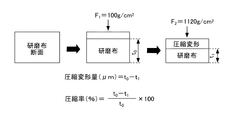
本発明において、研磨パッドの圧縮変形量とは、図7に示すように、研磨パッド(研磨布)の厚み方向に、F1=100g/cm2の荷重をかけたときの研磨パッドの厚みをt0とし、次いで、F2=1120g/cm2の荷重をかけたときの研磨パッドの厚みをt1としたときに、圧縮変形量(μm)=t0−t1で表されるものである。また、圧縮率(%)=[(t0−t1)/t0]×100で表される。この圧縮変形量の測定は、例えば図6示すように、定盤上に研磨パッドを載置し、研磨パッド上部から圧子(φ10mm)をストロークスピード0.1mm/minで押圧する、圧縮試験器を用いて行う。 In the present invention, the amount of compressive deformation of the polishing pad is the thickness of the polishing pad when a load of F 1 = 100 g / cm 2 is applied in the thickness direction of the polishing pad (polishing cloth) as shown in FIG. t 0, and then the thickness of the polishing pad when a load of F 2 = 1120 g / cm 2 is applied, where t 1 is the amount of compressive deformation (μm) = t 0 −t 1 is there. The compression ratio (%) = [(t 0 −t 1 ) / t 0 ] × 100. For example, as shown in FIG. 6, the compression deformation is measured by using a compression tester in which a polishing pad is placed on a surface plate and an indenter (φ10 mm) is pressed at a stroke speed of 0.1 mm / min from above the polishing pad. To do.
また、本発明において、樹脂モジュラスとは、樹脂自体の硬さを表す指標である。無発泡の樹脂フィルムを2倍に伸ばした際にかかる力(引張り応力)で表し、硬い樹脂ほど、伸ばすのに力が必要なので数値が大きくなる。柔らかい樹脂ほど、数値が小さくなる。樹脂モジュラスの測定方法を以下に示す。
(1)樹指溶液を薄く引き延ばし熱風乾燥し、50μm程度の厚みの乾式フィルムを作製する。
(2)フィルム作製後しばらく養生する。
(3)測定部の長さ20mm、幅5mm、厚さ0.05mmの短冊状試料を、引っ張り速度300mm/分で引っ張る。
(4)100%伸長特(2倍延伸時)の張力を試料の初期断面積で割り、100%モジュラス(MPa表示)を求める。
(5)試料数n=7の平均値を求める。
In the present invention, the resin modulus is an index representing the hardness of the resin itself. The value is expressed by the force (tensile stress) applied when the non-foamed resin film is stretched twice, and the harder the resin, the larger the numerical value because the force is required to stretch. The softer the resin, the smaller the value. The method for measuring the resin modulus is shown below.
(1) The resin solution is stretched thinly and dried with hot air to produce a dry film having a thickness of about 50 μm.
(2) Curing for a while after film production.
(3) A strip-shaped sample having a length of 20 mm, a width of 5 mm, and a thickness of 0.05 mm is pulled at a pulling speed of 300 mm / min.
(4) Divide the tension of the 100% elongation characteristic (at the time of double stretching) by the initial cross-sectional area of the sample to obtain 100% modulus (in MPa).
(5) The average value of the number of samples n = 7 is obtained.
樹脂モジュラスは、樹脂の系統(ポリカーボネート系、ポリエステル系、ポリエーテル系などの樹脂の種類)ではなく、基本的にハードセグメントの含有量で決まる。詳しくは、ポリウレタンは、ソフトセグメントとハードセグメントとを有しミクロ相分離構造をとっているため、そのハードセグメントの割合(量)で樹脂の硬さは決まる。ハードセグメントは、イソシアネートおよび低分子ジオールであり、樹脂(高分子)が強く凝集している箇所で、高分子=ソフトセグメントの動きが固定されている箇所である。ソフトセグメントは、高分子ポリオールであり、樹脂(高分子)が弱く凝集している箇所である。ソフトセグメントは、樹脂の系統(ポリカーボネート系、ポリエステル系、ポリエーテル系などの樹脂の種類)と樹脂のブレンド比で調整できる。 The resin modulus is basically determined not by the resin system (type of resin such as polycarbonate, polyester or polyether) but by the hard segment content. Specifically, since polyurethane has a soft segment and a hard segment and has a microphase separation structure, the hardness of the resin is determined by the ratio (amount) of the hard segment. The hard segment is an isocyanate and a low molecular diol, where the resin (polymer) is strongly aggregated, and where the movement of the polymer = soft segment is fixed. The soft segment is a polymer polyol and is a portion where the resin (polymer) is weakly aggregated. The soft segment can be adjusted by the blend ratio of the resin system (polycarbonate, polyester, polyether, etc.) and the resin.
上記のとおり、本発明者は、前記課題を解決するためには、鋭意検討の結果、研磨工程に適用する研磨パッドの圧縮変形量が330μm以下であり、ナップ層を形成する樹脂の100%モジュラスが3MPa以上14MPa以下であることが最適であることを見出した。研磨パッドの圧縮変形量が330μm超であると、例えばうねりPV値が10nm以上となり、うねりを抑制することができない。一方、ナップ層を形成する樹脂の100%モジュラスが3MPa未満であると、うねりを抑制することが困難である。また、100%モジュラスが14MPa超であると、うねりは抑制することができるものの、研磨後の基板表面に傷欠陥が多く発生してしまうという問題がある。 As described above, in order to solve the above problems, the present inventor has intensively studied and the amount of compressive deformation of the polishing pad applied to the polishing step is 330 μm or less, and the 100% modulus of the resin forming the nap layer Has been found to be optimal when it is 3 MPa or more and 14 MPa or less. When the amount of compressive deformation of the polishing pad exceeds 330 μm, for example, the undulation PV value becomes 10 nm or more, and the undulation cannot be suppressed. On the other hand, when the 100% modulus of the resin forming the nap layer is less than 3 MPa, it is difficult to suppress swell. Further, when the 100% modulus exceeds 14 MPa, undulation can be suppressed, but there is a problem that many scratch defects are generated on the polished substrate surface.
本発明においては、研磨パッドの圧縮変形量が、特に60μm以上300μm以下であることが好ましく、さらに好ましくは、75μm以上260μm以下である。また、ナップ層を形成する樹脂の100%モジュラスが、6MPa以上12MPa以下であることが特に好ましい。
近年、EUVリソグラフィーに適用される転写マスクには、30nm以下の平坦度が求められている。上記特性を備えた研磨パッドを使用して基板表面の研磨加工を行うことにより、研磨加工後の基板表面のうねりの発生を抑制でき、その結果、上述の転写マスクにおいて30nm以下の平坦度を実現できるような高い平坦度の基板を製造することが可能となる。
In the present invention, the amount of compressive deformation of the polishing pad is particularly preferably 60 μm or more and 300 μm or less, and more preferably 75 μm or more and 260 μm or less. The 100% modulus of the resin forming the nap layer is particularly preferably 6 MPa or more and 12 MPa or less.
In recent years, a flatness of 30 nm or less is required for a transfer mask applied to EUV lithography. By polishing the substrate surface using a polishing pad having the above characteristics, the occurrence of waviness on the substrate surface after polishing can be suppressed, and as a result, a flatness of 30 nm or less is realized in the transfer mask described above. It is possible to manufacture a substrate having such a high flatness as possible.
本発明に係るEUVリソグラフィー用マスクブランク用基板の製造方法では、上述の特性を備えた研磨パッドを適用した研磨工程を行うが、具体的には、回転面に研磨パッドを備える定盤に、基板をセットし、前記研磨パッドと前記基板との間にシリカ又はコロイダルシリカの研磨砥粒を含む研磨液を供給しつつ、前記研磨パッドの研磨面に対して前記基板を相対移動させ、前記基板の主表面を研磨する研磨工程である。
このような研磨工程は、例えば図5に示すような遊星歯車方式の両面研磨装置を使用して行うことができる。図5に示す両面研磨装置は、太陽歯車12と、その外方に同心円状に配置される内歯歯車13と、太陽歯車12及び内歯歯車13に噛み合い、太陽歯車12や内歯歯車13の回転に応じて公転及び自転するキャリア14と、このキャリア14に保持された被研磨加工物(上記基板1)を挟持可能な研磨パッド17がそれぞれ貼着された上定盤15及び下定盤16と、上定盤15と下定盤16との間に研磨液を供給する研磨液供給部(図示せず)とを備えている。
In the method for manufacturing a mask blank substrate for EUV lithography according to the present invention, a polishing step is performed by applying a polishing pad having the above-mentioned characteristics. Specifically, the substrate is mounted on a surface plate having a polishing pad on a rotating surface. The substrate is moved relative to the polishing surface of the polishing pad while supplying a polishing liquid containing abrasive grains of silica or colloidal silica between the polishing pad and the substrate. This is a polishing step for polishing the main surface.
Such a polishing process can be performed using, for example, a planetary gear type double-side polishing apparatus as shown in FIG. The double-side polishing apparatus shown in FIG. 5 meshes with the sun gear 12, the internal gear 13 arranged concentrically on the outer side thereof, the sun gear 12 and the internal gear 13, and the sun gear 12 and the internal gear 13. An upper surface plate 15 and a lower surface plate 16 to which a carrier 14 that revolves and rotates according to rotation, and a
このような両面研磨装置によって、研磨加工時には、キャリア14に保持された被研磨加工物、即ち基板(ガラス基板)1を上定盤15及び下定盤16とで挟持するとともに、上下定盤15,16の研磨パッド17と基板1との間に研磨液を供給しながら、太陽歯車12や内歯歯車13の回転に応じてキャリア14が公転及び自転しながら、基板1の上下両主表面が研磨加工される。このような両面研磨装置を用いることにより、基板の両主表面を同時に研磨することが可能であるが、本発明では、片面研磨装置で基板の両主表面を片面ずつ研磨するようにしてもよい。
With such a double-side polishing apparatus, during polishing processing, the workpiece to be polished, that is, the substrate (glass substrate) 1 is sandwiched between the upper surface plate 15 and the lower surface plate 16, and the upper and lower surface plates 15, The upper and lower main surfaces of the
本発明において、上記基板は、EUV露光用、つまりEUVリソグラフィー用マスクブランク用基板であり、露光時の熱によるパターンの歪みを防止するため、0±1.0×10⁻⁷/℃の範囲内、より好ましくは0±0.3×10−7/℃の範囲内の低熱膨張係数を有するものが好ましく用いられる。この範囲の低熱膨張係数を有する基板としては、多成分系ガラス基板が好ましく用いられる。具体的には、例えば、SiO2−TiO2系ガラス基板、多成分系ガラスセラミックス等を用いることが出来る。 In the present invention, the substrate is a substrate for EUV exposure, that is, a mask blank for EUV lithography, and in the range of 0 ± 1.0 × 10 −7 / ° C. in order to prevent distortion of the pattern due to heat during exposure. More preferably, those having a low thermal expansion coefficient within the range of 0 ± 0.3 × 10 −7 / ° C. are preferably used. As the substrate having a low thermal expansion coefficient in this range, a multicomponent glass substrate is preferably used. Specifically, for example, a SiO 2 —TiO 2 glass substrate, a multicomponent glass ceramic, or the like can be used.
本発明においては、例えば上記両面研磨装置を用いて、粗研磨工程、精密研磨工程、超精密研磨工程を行うことが望ましい。また、本発明では、超精密研磨工程において、上述の特性を有する研磨パッドを適用することが好ましい。
使用する研磨剤の種類や粒径は、基板材料や得ようとする平坦度に応じて適宜選定することができる。研磨剤としては、酸化セリウム、酸化ジルコニウム、シリカ、コロイダルシリカなどが挙げられる。研磨剤の粒径は、数十nmから数μmである。本発明のマスクブランク用基板の製造方法は、シリカ又はコロイダルシリカを含有する研磨液で基板を研磨する場合に最適な構成である。
In the present invention, it is desirable to perform a rough polishing process, a precision polishing process, and an ultraprecision polishing process using, for example, the above-described double-side polishing apparatus. Moreover, in this invention, it is preferable to apply the polishing pad which has the above-mentioned characteristic in an ultraprecision polishing process.
The type and particle size of the abrasive used can be appropriately selected according to the substrate material and the flatness to be obtained. Examples of the abrasive include cerium oxide, zirconium oxide, silica, colloidal silica, and the like. The particle size of the abrasive is several tens of nm to several μm. The method for producing a mask blank substrate of the present invention has an optimum configuration when the substrate is polished with a polishing liquid containing silica or colloidal silica.
上記粗研磨工程は、研削工程で形成された基板主表面の傷を除去し、研削工程で得られた平坦度を維持する目的として行われるもので、研磨砥粒の平均粒径が約1〜3μmの比較的大きな研磨砥粒を用いて研磨する工程である。研磨砥粒の材質は、基板の材料に応じて適宜選択される。粗研磨工程で使用する研磨パッドは、平坦度の維持の点から、硬質ポリシャを使用することが好ましい。 The rough polishing step is performed for the purpose of removing scratches on the main surface of the substrate formed in the grinding step and maintaining the flatness obtained in the grinding step. This is a step of polishing using relatively large abrasive grains of 3 μm. The material of the abrasive grains is appropriately selected according to the material of the substrate. The polishing pad used in the rough polishing step is preferably a hard polisher from the viewpoint of maintaining flatness.
上記精密研磨工程は、傷等の表面欠陥がなく、基板の鏡面化を目的として行われるもので、研磨砥粒の平均粒径が約1μm以下(例えば、10nm〜1μm)の比較的小さな研磨砥粒を用いて研磨する工程である。研磨砥粒の材質は、上述と同様に基板の材料に応じて適宜選択される。平均粒径が小さく平滑な基板表面が得られる点から酸化セリウムが好ましい。精密研磨工程で使用する研磨パッドは、鏡面化の点から、軟質または超軟質ポリシャを使用することが好ましい。 The precision polishing step is performed for the purpose of mirror-finishing the substrate without surface defects such as scratches, and a relatively small polishing abrasive having an average grain size of polishing abrasive grains of about 1 μm or less (for example, 10 nm to 1 μm). This is a step of polishing using grains. The material of the abrasive grains is appropriately selected according to the material of the substrate as described above. Cerium oxide is preferred from the viewpoint of obtaining a smooth substrate surface with a small average particle diameter. The polishing pad used in the precision polishing step is preferably a soft or ultra-soft polisher from the viewpoint of mirror finish.
上記超精密研磨工程は、基板の更なる鏡面化(表面粗さの向上)を目的として行われるもので、研磨砥粒の平均粒径が約500nm以下(例えば、10nm〜500nm)の非常に小さな研磨砥粒を用いて研磨する工程である。研磨砥粒の材質は、上述と同様に基板の材料に応じて適宜選択される。平均粒径が小さく平滑な基板表面が得られる点からシリカ又はコロイダルシリカが好ましい。超精密研磨工程で使用する研磨パッドは、更なる鏡面化の点から、軟質または超軟質ポリシャを使用することが好ましく、また本発明ではうねり低減の観点から、上述の圧縮変形量と100%モジュラス値を備えた研磨パッドを使用する。 The ultra-precise polishing step is performed for the purpose of further mirroring the substrate (improving the surface roughness), and the average particle size of the abrasive grains is very small, about 500 nm or less (for example, 10 nm to 500 nm). This is a step of polishing using abrasive grains. The material of the abrasive grains is appropriately selected according to the material of the substrate as described above. Silica or colloidal silica is preferable from the viewpoint of obtaining a smooth substrate surface having a small average particle diameter. The polishing pad used in the ultra-precision polishing process is preferably a soft or ultra-soft polisher from the viewpoint of further mirroring. In the present invention, from the viewpoint of reducing waviness, the above-mentioned compression deformation amount and 100% modulus are used. Use a polishing pad with a value.
本発明においては、上述の研磨工程の後に、ガラス基板主表面の表面形態情報(例えば凹凸形状)を測定する表面形態情報測定工程と、前記表面形態情報測定工程で得られた測定結果に基づいて、所望の平坦度となるように前記主表面の場所ごとに加工条件を設定して局所加工する局所加工工程と、前記局所加工工程の後、所望の平滑度となるように仕上げ研磨する仕上げ研磨工程とを行うことが好ましい。これにより、上記構成1による研磨加工後のうねりの発生を抑制した基板表面を維持しつつ、かつ深さの浅い傷が除去されて傷欠陥も低減でき、高平坦度(例えば30nm以下)の基板を製造することが可能である。
In the present invention, after the above-described polishing step, based on the surface shape information measuring step for measuring the surface shape information (for example, uneven shape) of the main surface of the glass substrate and the measurement result obtained in the surface shape information measuring step. A local processing step for setting a processing condition for each location on the main surface so as to obtain a desired flatness, and a local polishing step for performing a local polishing after the local processing step so as to obtain a desired smoothness. It is preferable to perform a process. Thereby, while maintaining the substrate surface in which the occurrence of waviness after polishing by the above-described
上記表面形態情報測定工程は、上記研磨工程によって得られたガラス基板主表面の凹凸形状(平坦度)を測定する工程である。ガラス基板主表面の凹凸形状の測定には、通常、光学干渉計が使用される。光学干渉計には、たとえばフリンジ観察干渉計や位相シフト干渉計などがある。上記光学干渉計によって測定された凹凸形状の測定結果は、コンピュータなどの記録媒体に保存される。
次に、コンピュータなどの演算処理手段によって、凹凸形状の測定結果と予め設定された所定の基準値(所望の平坦度)とが比較され、その差分がガラス基板表面の所定領域(例えば縦5mm×横5mmの領域)ごとに算出される。すなわち、ガラス基板表面の凸部分の高さに応じて加工取り代が設定される。この差分(加工取り代)が、局所的な表面加工における各所定領域の必要除去量とされる。
The surface form information measuring step is a step of measuring the uneven shape (flatness) of the main surface of the glass substrate obtained by the polishing step. An optical interferometer is usually used for measuring the irregular shape of the main surface of the glass substrate. Examples of the optical interferometer include a fringe observation interferometer and a phase shift interferometer. The measurement result of the concavo-convex shape measured by the optical interferometer is stored in a recording medium such as a computer.
Next, the measurement result of the concavo-convex shape is compared with a predetermined reference value (desired flatness) by an arithmetic processing means such as a computer, and the difference is a predetermined area on the surface of the glass substrate (for example, 5 mm in length × It is calculated for each area of 5 mm in width. That is, the machining allowance is set according to the height of the convex portion on the surface of the glass substrate. This difference (machining allowance) is used as a necessary removal amount for each predetermined region in local surface machining.
上記局所加工工程は、上記演算処理によって設定された加工取り代に応じた加工条件で、所定領域毎に凸部分を局所加工し、ガラス基板主表面の平坦度を所定の基準値以下に制御する工程である。
局所的な表面加工法としては、鉄を含む磁性流体中に研磨砥粒を含有させた磁性研磨スラリーを用いて、ガラス基板表面に局所的に接触させるMRF(Magneto Rheological Finishing)加工法を用いることができる。MRF加工法以外にも、GCIB(ガスクラクターイオンビーム)やプラズマエッチングによる局所加工法を用いてもよい。
In the local processing step, the convex portion is locally processed for each predetermined region under a processing condition according to the processing allowance set by the arithmetic processing, and the flatness of the glass substrate main surface is controlled to a predetermined reference value or less. It is a process.
As a local surface processing method, an MRF (Magneto Rheological Finishing) processing method is used in which a magnetic polishing slurry containing abrasive grains in a magnetic fluid containing iron is used to locally contact the glass substrate surface. Can do. In addition to the MRF processing method, a local processing method using GCIB (gas crater ion beam) or plasma etching may be used.
次に、洗浄工程を行うことが好適である。ガラス基板の洗浄方法は特に制約されないが、上記局所加工工程においてMRF加工法を用いた場合には、磁性流体に含有された鉄成分が微量ではあるが、ガラス基板表面に付着している場合があるので、例えば塩酸などを用いた酸洗浄を行い、基板表面に付着した鉄成分を溶解除去することが望ましい。
洗浄方法としては、洗浄槽にガラス基板を浸漬させるディップ法や、洗浄液をノズルで基板表面に供給する方法など、任意である。さらに必要に応じて、超音波を印加したり、スクラブ洗浄により洗浄力を高めるようにしてもよい。
Next, it is preferable to perform a cleaning process. The method for cleaning the glass substrate is not particularly limited, but when the MRF processing method is used in the local processing step, the iron component contained in the magnetic fluid is very small, but may adhere to the glass substrate surface. Therefore, it is desirable to perform acid cleaning using, for example, hydrochloric acid to dissolve and remove the iron component adhering to the substrate surface.
As a cleaning method, a dipping method in which a glass substrate is immersed in a cleaning tank, a method of supplying a cleaning liquid to the substrate surface with a nozzle, and the like are arbitrary. Furthermore, if necessary, the cleaning power may be increased by applying ultrasonic waves or scrub cleaning.
上記仕上げ研磨工程は、上述の局所加工工程において、ガラス基板表面に面荒れや加工変質層が生じた場合、これらの除去を目的として行うものであり、ガラス基板表面に除去が必要な面荒れや加工変質層が生じていない場合には、仕上げ研磨は特に行わなくてもよい。
この仕上げ研磨の方法としては、局所加工工程で得られた平坦度を維持しつつ、表面粗さが改善される研磨方法が好ましい。例えば、研磨パッドなどの研磨用工具面をガラス基板主表面と接触させて研磨液により精密研磨する方法や、ガラス基板主表面と研磨用工具面が直接接触することなく、両者の間に介在する加工液の作用で研磨を行う非接触研磨方法(例えば、フロートポリッシング法、EEM(Elastic Emission Machining)法)などが挙げられる。
In the above-mentioned local processing step, the finish polishing step is performed for the purpose of removing a surface roughness or a work-affected layer on the surface of the glass substrate. When the work-affected layer is not generated, the finish polishing is not particularly required.
As this finish polishing method, a polishing method in which the surface roughness is improved while maintaining the flatness obtained in the local processing step is preferable. For example, a polishing tool surface such as a polishing pad is brought into contact with the glass substrate main surface and precisely polished with a polishing liquid, or the glass substrate main surface and the polishing tool surface are not directly in contact with each other Non-contact polishing methods (for example, a float polishing method, an EEM (Elastic Emission Machining) method) in which polishing is performed by the action of a working fluid can be used.
上記基板1の転写パターンが形成される側の主表面は、少なくともパターン転写精度、位置精度を得る観点から高平坦度となるように表面加工される。本発明においては、基板の転写パターンが形成される側の主表面132mm×132mmの領域において、平坦度が30nm以下であることが好ましく、さらに好ましくは25nm以下、特に好ましくは20nm以下である。また、転写パターンが形成される側と反対側の主表面は、露光装置にセットする時に静電チャックされる面であって、132mm×132mmの領域において、平坦度が30nm以下、好ましくは25nm以下である。
また、EUV露光用の場合、基板1として要求される表面平滑度は、基板の転写パターンが形成される側の主表面の表面粗さが、二乗平均平方根粗さ(RMS)で0.15nm以下、さらに好ましくは0.10nm以下であることが好ましい。
The main surface of the
In the case of EUV exposure, the surface smoothness required for the
[EUVリソグラフィー用多層反射膜付き基板]
次に、本発明に係る多層反射膜付き基板について説明する。
図1は、本発明に係る多層反射膜付き基板の層構成を示す断面図であり、基板1の上に、露光光であるEUV光を反射する多層反射膜2を備えた構造の多層反射膜付き基板10を示す。
上記基板1は、上述のEUVリソグラフィー用マスクブランク用基板である。このマスクブランク用基板については上述したとおりであるので、ここでは説明を省略する。
[Substrate with multilayer reflective film for EUV lithography]
Next, the substrate with a multilayer reflective film according to the present invention will be described.
FIG. 1 is a cross-sectional view showing a layer structure of a substrate with a multilayer reflective film according to the present invention. The multilayer reflective film has a multilayer
The
上記多層反射膜2は、屈折率の異なる元素が周期的に積層された多層膜であり、一般的には、低屈折率材料である重元素又はその化合物の薄膜(低屈折率層)と、高屈折率材料である軽元素又はその化合物の薄膜(高屈折率層)とが交互に40〜60周期程度積層された多層膜が用いられる。多層膜は、基板側から高屈折率層と低屈折率層をこの順に積層した積層構造を1周期として複数周期積層しても良いし、基板側から低屈折率層と高屈折率層をこの順に積層した積層構造を1周期として複数周期積層しても良い。低屈折率材料としては、Mo、Ru、Rh、Ptから選ばれる元素やこれらの合金が用いられ、高屈折率材料としては、Si又はSi化合物が用いられる。例えば、波長13〜14nmのEUV光に対する多層反射膜としては、好ましくは、Mo膜とSi膜を交互に40〜60周期程度積層したMo/Si周期積層膜が好ましく用いられる。
The multilayer
上記多層反射膜2は、例えばイオンビームスパッタリング法により、各層を成膜することにより形成できる。上述したMo/Si周期多層膜の場合、例えばイオンビームスパッタリング法により、まずSiターゲットを用いて厚さ数nm程度のSi膜を成膜し、その後Moターゲットを用いて厚さ数nm程度のMo膜を成膜し、これを一周期として、40〜60周期積層した後、最後に、Si膜を成膜する。
上述の本発明に係る製造方法により得られるマスクブランク用基板の主表面上に、露光光を反射する多層反射膜を形成することにより、基板表面のうねり等に起因する欠陥の無いEUVリソグラフィー用多層反射膜付き基板を得ることができる。
The multilayer
A multilayer reflective film that reflects exposure light is formed on the main surface of a mask blank substrate obtained by the above-described manufacturing method according to the present invention, so that a multilayer for EUV lithography free from defects caused by waviness on the substrate surface is formed. A substrate with a reflective film can be obtained.
[EUVリソグラフィー用マスクブランク]
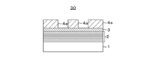
また、本発明は、上述の本発明の製造方法により製造した多層反射膜付き基板を用いるEUVリソグラフィー用マスクブランクの製造方法についても提供する。
図2は、マスクブランクの層構成を示す断面図であり、基板1上に、EUV光を反射する多層反射膜2、保護膜(キャッピング層)3、及び転写パターン形成用薄膜として、EUV光を吸収する吸収体膜4が形成されているEUVリソグラフィー用反射型マスクブランク20を示す。なお、図示していないが、基板1の多層反射膜等が形成されている側とは反対側に裏面導電膜を設けることができる。
なお、上記基板1上に多層反射膜を形成した状態の多層反射膜付き基板については上述したとおりであり、ここでは説明を省略する。
[Mask blank for EUV lithography]
The present invention also provides a method for manufacturing a mask blank for EUV lithography using a substrate with a multilayer reflective film manufactured by the above-described manufacturing method of the present invention.
FIG. 2 is a cross-sectional view showing the layer structure of the mask blank. On the
The substrate with the multilayer reflective film in the state where the multilayer reflective film is formed on the
通常、上記吸収体膜4のパターニング或いはパターン修正の際に多層反射膜2を保護する目的で、多層反射膜2と吸収体膜4との間に上記保護膜3やバッファ膜を設ける。保護膜3の材料としては、ケイ素のほか、ルテニウムや、ルテニウムにニオブ、ジルコニウム、ロジウムのうち1以上の元素を含有するルテニウム化合物が用いられ、バッファ膜の材料としては、主にクロム系材料が用いられる。
このような保護膜3やバッファ膜は、マグネトロンスパッタリングなどのスパッタ法で形成するのが好ましい。
Usually, the
The
上記吸収体膜4は、露光光である例えばEUV光を吸収する機能を有するもので、例えばタンタル(Ta)単体又はTaを主成分とする材料を好ましく用いることができる。Taを主成分とする材料は、通常、Taの合金である。このような吸収体膜の結晶状態は、平滑性、平坦性の点から、アモルファス状又は微結晶の構造を有しているものが好ましい。
Taを主成分とする材料としては、TaとBを含む材料、TaとNを含む材料、TaとBを含み、更にOとNの少なくとも何れかを含む材料、TaとSiを含む材料、TaとSiとNを含む材料、TaとGeを含む材料、TaとGeとNを含む材料、等を用いることが出来る。TaにBやSi、Ge等を加えることにより、アモルファス状の材料が容易に得られ、平滑性を向上させることができる。また、TaにNやOを加えれば、酸化に対する耐性が向上するため、経時的な安定性を向上させることが出来るという効果が得られる。
The absorber film 4 has a function of absorbing exposure light such as EUV light. For example, tantalum (Ta) alone or a material mainly composed of Ta can be preferably used. The material mainly composed of Ta is usually an alloy of Ta. Such an absorber film preferably has an amorphous or microcrystalline structure in terms of smoothness and flatness.
As a material having Ta as a main component, a material containing Ta and B, a material containing Ta and N, a material containing Ta and B and further containing at least one of O and N, a material containing Ta and Si, Ta A material containing Si and N, a material containing Ta and Ge, a material containing Ta, Ge and N can be used. By adding B, Si, Ge or the like to Ta, an amorphous material can be easily obtained and the smoothness can be improved. Further, when N or O is added to Ta, resistance to oxidation is improved, so that an effect that stability with time can be improved is obtained.
この中でも特に好ましい材料として、例えば、TaとBを含む材料(組成比Ta/Bが8.5/1.5〜7.5/2.5の範囲である)、TaとBとNを含む材料(Nが5〜30原子%であり、残りの成分を100とした時、Bが10〜30原子%)が挙げられる。これらの材料の場合、容易に微結晶或いはアモルファス構造を得ることが出来、良好な平滑性と平坦性が得られる。
このようなTa単体又はTaを主成分とする吸収体膜は、マグネトロンスパッタリングなどのスパッタ法で形成するのが好ましい。例えば、TaBN膜の場合、タンタルとホウ素を含むターゲットを用い、窒素を添加したアルゴンガスを用いたスパッタリング法で成膜することができる。
Among these, as a particularly preferable material, for example, a material containing Ta and B (composition ratio Ta / B is in the range of 8.5 / 1.5 to 7.5 / 2.5), Ta, B and N are included. Materials (N is 5 to 30 atomic%, and B is 10 to 30 atomic% when the remaining components are 100). In the case of these materials, a microcrystalline or amorphous structure can be easily obtained, and good smoothness and flatness can be obtained.
Such an absorber film containing Ta alone or Ta as a main component is preferably formed by a sputtering method such as magnetron sputtering. For example, in the case of a TaBN film, a target containing tantalum and boron can be used and a film can be formed by a sputtering method using an argon gas to which nitrogen is added.
吸収体膜として、Taを主成分とする材料以外では、例えば、WN、TiN、Ti等の材料が挙げられる。
吸収体膜4の膜厚は、露光光である例えばEUV光が十分に吸収できる厚みであれば良いが、通常30〜100nm程度である。なお、吸収体膜4は、材料や組成の異なる複数層の積層構造(例えばTaBN膜とTaBO膜の積層膜)としてもよい。
As the absorber film, materials other than materials mainly composed of Ta include materials such as WN, TiN, and Ti.
The thickness of the absorber film 4 may be a thickness that can sufficiently absorb, for example, EUV light as exposure light, but is usually about 30 to 100 nm. The absorber film 4 may have a laminated structure of a plurality of layers having different materials and compositions (for example, a laminated film of a TaBN film and a TaBO film).
EUV光を露光光に適用する反射型マスクの場合においても、パターン検査を行う時の検査光は、波長193nm、257nm等のEUV光に比べて長波長の光が用いられる場合が多い。長波長の検査光に対応するためには、吸収体膜の表面反射を低減させる必要がある。この場合、吸収体膜を、基板側から、主としてEUV光を吸収する機能を有する吸収体層と、主として検査光に対する表面反射を低減する機能を有する低反射層とを積層した構成にするとよい。低反射層としては、吸収体層がTaを主成分とする材料の場合、TaやTaBにOを含有した材料が好適である。
また、上記反射型マスクブランクは、吸収体膜に所定の転写パターンを形成するためのレジスト膜が形成された状態であっても構わない。
Even in the case of a reflective mask that applies EUV light to exposure light, the inspection light used for pattern inspection is often light having a longer wavelength than EUV light having a wavelength of 193 nm, 257 nm, or the like. In order to deal with long-wavelength inspection light, it is necessary to reduce the surface reflection of the absorber film. In this case, the absorber film may have a structure in which an absorber layer mainly having a function of absorbing EUV light and a low reflection layer mainly having a function of reducing surface reflection with respect to inspection light are laminated from the substrate side. As the low reflection layer, when the absorber layer is a material mainly composed of Ta, a material containing O in Ta or TaB is suitable.
The reflective mask blank may be in a state where a resist film for forming a predetermined transfer pattern is formed on the absorber film.
本発明によれば、例えば上述の本発明により得られる多層反射膜付き基板を用いてマスクブランクを製造することにより、基板表面のうねり等に起因する欠陥の無いEUVリソグラフィー用マスクブランクを得ることができる。 According to the present invention, for example, by manufacturing a mask blank using the multilayer reflective film-coated substrate obtained by the present invention described above, it is possible to obtain a mask blank for EUV lithography that is free from defects caused by waviness or the like of the substrate surface. it can.
[EUVリソグラフィー用転写マスク]
また、本発明は、上記構成のマスクブランクを用いるEUVリソグラフィー用転写マスクの製造方法についても提供する。
図3は転写マスクの層構成を示す断面図であり、図2のマスクブランク20における吸収体膜4がパターニングされた吸収体膜パターン4aを備えるEUVリソグラフィー用反射型マスク30を示す。
図2のマスクブランク20における転写パターンとなる上記吸収体膜4をパターニングする方法は、高精細のパターニングを行うことができるフォトリソグラフィー法が最も好適である。
[Transfer mask for EUV lithography]
The present invention also provides a method of manufacturing a transfer mask for EUV lithography using the mask blank having the above-described configuration.
FIG. 3 is a cross-sectional view showing a layer structure of the transfer mask, and shows a
As a method for patterning the absorber film 4 to be a transfer pattern in the
上述の本発明のマスクブランクを用いて反射型マスクを製造することにより、基板表面のうねり等に起因する欠陥がなく、パターン精度の良好なパターン転写を実現できるEUVリソグラフィー用転写マスクを得ることができる。 By manufacturing a reflective mask using the above-described mask blank of the present invention, it is possible to obtain a transfer mask for EUV lithography that can realize pattern transfer with good pattern accuracy without defects caused by waviness of the substrate surface. it can.
以下、実施例により、本発明の実施の形態を更に具体的に説明する。
(実施例1〜5、比較例1〜3)
<EUVリソグラフィー用マスクブランク用基板の作製>
(1)粗研磨工程
端面を面取り加工し、両面ラッピング装置によって研削加工を終えたSiO2−TiO2系ガラス基板(約152mm×約152mm×約6.3mm)を、上述の両面研磨装置に10枚セットし、以下の研磨条件で粗研磨工程を行った。なお、加工荷重、研磨時間は適宜調整して行った。
研磨液:酸化セリウム(平均粒径2〜3μm)+水
研磨パッド:硬質ポリシャ(ウレタンパッド)
上記粗研磨工程後、ガラス基板に付着した研磨砥粒を除去するため、ガラス基板を洗浄槽に浸漬(超音波印加)し、洗浄を行った。
Hereinafter, the embodiment of the present invention will be described more specifically with reference to examples.
(Examples 1-5, Comparative Examples 1-3)
<Preparation of mask blank substrate for EUV lithography>
(1) Rough Polishing Step A SiO 2 —TiO 2 glass substrate (about 152 mm × about 152 mm × about 6.3 mm) whose end face is chamfered and ground by a double-side lapping apparatus is applied to the above-mentioned double-side polishing apparatus. Sheets were set and a rough polishing process was performed under the following polishing conditions. The processing load and polishing time were adjusted as appropriate.
Polishing liquid: Cerium oxide (
After the rough polishing step, the glass substrate was immersed in a cleaning tank (ultrasonic application) in order to remove the abrasive grains adhering to the glass substrate and cleaned.
(2)精密研磨工程
上述の両面研磨装置を使用し、粗研磨工程を終えた上記10枚のガラス基板に対し、以下の研磨条件で精密研磨工程を行った。なお、加工荷重、研磨時間は適宜調整して行った。
研磨液:酸化セリウム(平均粒径1μm)+水
研磨パッド:軟質ポリシャ(ウレタンパッド)
上記精密研磨工程後、ガラス基板に付着した研磨砥粒を除去するため、ガラス基板を洗浄槽に浸漬(超音波印加)し、洗浄を行った。
(2) Precision polishing process The above-mentioned double-side polishing apparatus was used, and the above-mentioned 10 glass substrates that finished the rough polishing process were subjected to a precision polishing process under the following polishing conditions. The processing load and polishing time were adjusted as appropriate.
Polishing liquid: Cerium oxide (
After the precision polishing step, in order to remove abrasive grains adhering to the glass substrate, the glass substrate was immersed in a cleaning tank (application of ultrasonic waves) to perform cleaning.
(3)超精密研磨工程
上述の両面研磨装置を使用し、精密研磨工程を終えた上記10枚のガラス基板に対し、以下の研磨条件で超精密研磨工程を行った。なお、加工荷重、研磨時間は適宜調整して行った。
研磨液:コロイダルシリカ(1次粒子径:70nm)+水、濃度40vol%、pH:3。
研磨パッド:パッド構造、圧縮変形量、ナップ層の100%モジュラスが表1に記載の所定の特性を有する研磨パッドを使用。
なお、研磨パッドの基材は、PET樹脂フィルムまたは不織布とし、ナップ層はポリウレタン樹脂からなる。また、研磨パッドの圧縮変形量、ナップ層の100%モジュラスは前述の方法により測定した。
上記超精密研磨工程後、ガラス基板に付着した研磨砥粒(コロイダルシリカ)を除去するため、低濃度のケイフッ酸水溶液で洗浄後、純水によるリンスを行った。
(3) Ultra-precision polishing process Using the above-described double-side polishing apparatus, an ultra-precision polishing process was performed under the following polishing conditions on the ten glass substrates that had finished the precision polishing process. The processing load and polishing time were adjusted as appropriate.
Polishing liquid: colloidal silica (primary particle diameter: 70 nm) + water, concentration 40 vol%, pH: 3.
Polishing pad: A polishing pad in which the pad structure, the amount of compressive deformation, and the 100% modulus of the nap layer have the predetermined characteristics described in Table 1 is used.
The base material of the polishing pad is a PET resin film or a nonwoven fabric, and the nap layer is made of a polyurethane resin. Further, the amount of compressive deformation of the polishing pad and the 100% modulus of the nap layer were measured by the methods described above.
After the ultraprecision polishing step, in order to remove polishing abrasive grains (colloidal silica) adhering to the glass substrate, the substrate was washed with a low-concentration silicic acid solution and rinsed with pure water.
以上のようにして得られたガラス基板のうねりPV、キズ欠陥数、トータル欠陥数を以下のようにして測定し、その結果を表1に示した。
うねりPVについては、基板主表面の中心10mm×10mmの領域を、非接触表面形状測定機(Zygo社製 NewView6300)で測定した。基準線に対する最高点と最低点の高さの差をもって、うねりPV(nm)とした。なお、表1中のうねりPV(nm)の値は、基板10枚の平均値であり、小数点第二位を四捨五入した。
また、基板主表面の132mm×132mmの領域を、マスクブランクス欠陥検査装置(レーザーテック社製 MAGICS M6640)にて測定後、レビュー像により欠陥種類を特定し、基板1枚当りのキズ欠陥数とトータル欠陥数をカウントした。なお、表1中のキズ欠陥数とトータル欠陥数の値は、基板10枚の平均値であり、小数点第一位を四捨五入した。
The undulation PV, the number of scratch defects, and the total number of defects of the glass substrate obtained as described above were measured as follows, and the results are shown in Table 1.
For the undulation PV, the
In addition, after measuring a 132mm x 132mm area on the main surface of the substrate with a mask blank defect inspection device (MAGICS M6640 manufactured by Lasertec Corporation), the type of defect is specified by the review image, and the number of scratch defects per substrate and total defects Counted the number. The values of the number of scratch defects and the total number of defects in Table 1 are average values of 10 substrates, and the first decimal place is rounded off.

上記表1に示すとおり、研磨パッドの圧縮変形量の値が小さくなる、およびナップ層の100%モジュラスの値が大きくなるに従ってうねりのPV値が小さくなり、それにより基板主表面へのトータル欠陥数及びキズ欠陥数も大きくなっていることが確認できる。 As shown in Table 1 above, the PV value of the undulation decreases as the value of the amount of compressive deformation of the polishing pad decreases and the value of the 100% modulus of the nap layer increases, whereby the total number of defects on the main surface of the substrate. It can also be confirmed that the number of scratch defects is also increased.
次に、上述の粗研磨工程、精密研磨工程、超精密研磨工程を5バッチ(1バッチ10枚)行い、50枚のガラス基板を準備した。
続いて、このガラス基板の表裏両面の表面形状(表面形態、平坦度)を平坦度測定器(Corning Tropel社製UltraFlat200M)で測定した(測定領域132mm×132mm)。その結果、ガラス基板表面及び裏面の平坦度は約200nmであった。
ガラス基板表面の表面形状(平坦度)の測定結果は、測定点ごとにある基準面に対する高さの情報としてコンピュータに保存するとともに、ガラス基板を所望の平坦度にするための必要除去量をコンピュータで計算した。
Next, the above-described rough polishing process, precision polishing process, and ultra-precision polishing process were performed in 5 batches (1
Subsequently, the surface shape (surface morphology, flatness) of the front and back surfaces of the glass substrate was measured with a flatness measuring device (UltraFlat 200M manufactured by Corning Tropel) (measurement area 132 mm × 132 mm). As a result, the flatness of the front and back surfaces of the glass substrate was about 200 nm.
The measurement result of the surface shape (flatness) of the surface of the glass substrate is stored in a computer as height information with respect to a reference plane at each measurement point, and the necessary removal amount for making the glass substrate a desired flatness is calculated by the computer. Calculated with
次に、ガラス基板面内を加工スポット形状領域ごとに、必要除去量に応じた局所表面加工の加工条件を設定した。事前にダミー基板を用いて、実際の加工と同じようにダミー基板を、一定時間基板を移動させずにスポットで加工し、その形状を上記表裏面の表面形状を測定する装置と同じ測定機にて測定し、単位時間当たりにおけるスポットの加工体積を算出した。そして、スポットの情報とガラス基板の表面形状の情報より得られた必要除去量に従い、ガラス基板をラスタ走査する際の走査スピードを決定した。 Next, the processing conditions of the local surface processing according to the required removal amount were set for each processing spot shape region in the glass substrate surface. Using a dummy substrate in advance, the dummy substrate is processed with a spot without moving the substrate for a certain period of time in the same way as in actual processing, and the shape is converted to the same measuring machine as the apparatus for measuring the surface shape of the front and back surfaces. The spot processing volume per unit time was calculated. Then, according to the necessary removal amount obtained from the spot information and the surface shape information of the glass substrate, the scanning speed for raster scanning the glass substrate was determined.
設定した加工条件に従い、磁気流体による基板仕上げ装置を用いてMRF(磁気粘弾性流体)加工法により、ガラス基板の表裏面平坦度が上記の基準値以下となるように局所的表面加工処理をして表面形状を調整した。研磨スラリーは、酸化セリウムを使用した。局所加工後、仕上げ研磨を行った。
その後、ガラス基板を塩酸水溶液が入った洗浄槽に約10分間浸漬した後、純水によるリンス、イソプロピルアルコール(IPA)乾燥を行った。
以上のようにして、EUVマスクブランク用ガラス基板を得た。
According to the set processing conditions, local surface processing is performed by MRF (Magneco-Viscoelastic Fluid) processing method using a magnetic fluid substrate finishing device so that the flatness of the front and back surfaces of the glass substrate is below the above reference value. The surface shape was adjusted. As the polishing slurry, cerium oxide was used. After local processing, finish polishing was performed.
Thereafter, the glass substrate was immersed in a cleaning tank containing an aqueous hydrochloric acid solution for about 10 minutes, and then rinsed with pure water and isopropyl alcohol (IPA) dried.
As described above, an EUV mask blank glass substrate was obtained.
得られたガラス基板に対し、主表面の表面形状を平坦度測定器(Corning Tropel社製 UltraFlat200M)で測定した。また、ガラス基板主表面の132mm×132mmの領域を、マスクブランクス欠陥検査装置(レーザーテック社製 MAGICS M6640)にて測定後、レビュー像により欠陥種類を特定し、基板1枚当りのキズ欠陥数とトータル欠陥数をカウントした。なお、表2中のキズ欠陥数とトータル欠陥数の値は、基板50枚の平均値であり、小数点第一位を四捨五入した。
得られた基板について、132mm×132mm領域の平坦度30nm以下の歩留り、基板50枚中、最も良好な平坦度、キズ欠陥数、トータル欠陥数を纏めて表2に示した。
The surface shape of the main surface was measured with respect to the obtained glass substrate with a flatness measuring device (UltraFlat 200M manufactured by Corning Tropel). In addition, after measuring a 132 mm x 132 mm area on the main surface of the glass substrate with a mask blanks defect inspection device (MAGICS M6640 manufactured by Lasertec Corporation), the type of defect is identified from the review image, and the total number of scratch defects per substrate is determined. The number of defects was counted. The values of the number of scratch defects and the total number of defects in Table 2 are the average values of 50 substrates, and the first decimal place is rounded off.
The obtained substrate has a yield of a flatness of 30 nm or less in a 132 mm × 132 mm region, and the best flatness, the number of scratch defects, and the total number of defects among 50 substrates are shown in Table 2.
上記表2に示すとおり、超精密研磨工程で使用する研磨パッドの特性が本発明で規定する範囲の場合、超精密研磨工程後のガラス基板のうねりが小さく、また、形成されるキズの深さも比較的浅いため、歩留りは76%〜82%と高く、また、トータル欠陥数、キズ欠陥数も10個以下と良好であった。特に、研磨パッドの圧縮変形量が60μm以上300μm以下であって、且つ、ナップ層を構成する樹脂の100%モジュラスが6MPa以上12MPa以下の場合、歩留り、欠陥数ともに良好な値が得られた。 As shown in Table 2 above, when the characteristics of the polishing pad used in the ultra-precision polishing step are within the range specified in the present invention, the undulation of the glass substrate after the ultra-precision polishing step is small, and the depth of scratches formed is also Since it was relatively shallow, the yield was as high as 76% to 82%, and the total number of defects and the number of scratch defects were as good as 10 or less. In particular, when the amount of compressive deformation of the polishing pad was 60 μm or more and 300 μm or less and the 100% modulus of the resin constituting the nap layer was 6 MPa or more and 12 MPa or less, good values were obtained for both the yield and the number of defects.
一方、比較例1のように、超精密研磨工程で使用する研磨パッドのナップ層の硬度(100%モジュラス)が高い場合、うねりの値は非常に小さな値に抑えられ、平坦度30nm以下の歩留まりは高いが、超精密研磨工程により形成されるキズが深く、その後に行われた局所加工、仕上げ研磨でも取りきれずに、トータル欠陥数、キズ欠陥数ともに非常に多い値となった。これらの欠陥は、多層反射膜で完全に消すことができないため、多層反射膜付き基板や、反射型マスクブランクの欠陥となる。
また、比較例2、3のように、超精密研磨工程で使用する研磨パッドのナップ層の硬度(100%モジュラス)が低いか、又は、研磨パッドの圧縮変形量が大きい場合、トータル欠陥数、キズ欠陥数は非常に小さい値となったが、超精密研磨工程後のうねりが大きいため、平坦度30nm以下の歩留まりは46%(比較例2)、38%(比較例3)と低い値となった。
On the other hand, as in Comparative Example 1, when the hardness (100% modulus) of the nap layer of the polishing pad used in the ultraprecision polishing process is high, the waviness value is suppressed to a very small value and the yield is flatness of 30 nm or less. Although it was high, the scratches formed by the ultra-precision polishing process were deep, and even after the local processing and finish polishing performed thereafter, the total number of defects and the number of scratch defects were very high. Since these defects cannot be completely erased by the multilayer reflective film, they become defects of the substrate with the multilayer reflective film and the reflective mask blank.
Further, as in Comparative Examples 2 and 3, when the hardness (100% modulus) of the nap layer of the polishing pad used in the ultraprecision polishing process is low, or the amount of compressive deformation of the polishing pad is large, the total number of defects, Although the number of scratch defects was a very small value, since the waviness after the ultra-precision polishing process was large, the yield with a flatness of 30 nm or less was as low as 46% (Comparative Example 2) and 38% (Comparative Example 3). became.
<多層反射膜付き基板の作製>
上記の実施例1で得られたEUVマスクブランク用ガラス基板上に、以下のようにして多層反射膜を形成した。基板上に形成される多層反射膜は、13〜14nmの露光光波長帯域に適した多層反射膜とするために、Mo膜/Si膜周期多層反射膜を採用した。
即ち、多層反射膜は、MoターゲットとSiターゲットを使用し、イオンビームスパッタリングにより基板上に交互に積層して形成した。
<Production of substrate with multilayer reflective film>
A multilayer reflective film was formed on the glass substrate for EUV mask blank obtained in Example 1 as described below. As the multilayer reflective film formed on the substrate, a Mo film / Si film periodic multilayer reflective film was employed in order to obtain a multilayer reflective film suitable for an exposure light wavelength band of 13 to 14 nm.
That is, the multilayer reflective film was formed by alternately stacking on the substrate by ion beam sputtering using a Mo target and a Si target.
まず、Siターゲットを用いて、Si膜を4.2nm成膜した。続いて、Moターゲットを用いて、Mo膜を2.8nm成膜した。これを一周期として40周期積層した後、Si膜を4.2nm成膜した。さらに、その上に、RuNbからなる保護膜(膜厚2.5nm)をイオンビームスパッタリング法によって成膜した。
この保護膜表面に対し、13.5nmのEUV光を入射角6.0度で反射率を測定したところ、反射率は63%であった。
以上のようにして、多層反射膜付き基板を作製した。
この得られた多層反射膜付き基板の主表面の表面粗さは、二乗平均平方根粗さ(RMS)で、0.13nmと良好であった。
First, a Si film was formed to 4.2 nm using a Si target. Subsequently, a Mo film was formed to 2.8 nm using a Mo target. After 40 periods were laminated with this as one period, a Si film was formed to 4.2 nm. Furthermore, a protective film (film thickness: 2.5 nm) made of RuNb was formed thereon by ion beam sputtering.
When the reflectance of this protective film surface was measured with 13.5 nm EUV light at an incident angle of 6.0 degrees, the reflectance was 63%.
A substrate with a multilayer reflective film was produced as described above.
The surface roughness of the main surface of the obtained multilayer reflective film-coated substrate was as good as 0.13 nm in terms of root mean square roughness (RMS).
<EUVリソグラフィー用反射型マスクブランクの作製>
上記で作製した多層反射膜付き基板の保護膜上に、吸収体膜として、TaBN膜(膜厚56nm)とTaBO膜(膜厚14nm)の積層膜をDCマグネトロンスパッタリング法によって成膜した。
こうして、EUVリソグラフィー用反射型マスクブランクを作製した。
<Preparation of a reflective mask blank for EUV lithography>
A laminated film of a TaBN film (film thickness of 56 nm) and a TaBO film (film thickness of 14 nm) was formed as an absorber film on the protective film of the substrate with a multilayer reflective film produced above by a DC magnetron sputtering method.
Thus, a reflective mask blank for EUV lithography was produced.
<EUVリソグラフィー用反射型マスクの作製>
次に、この反射型マスクブランクを用いて、半導体デザインルールにおけるDRAM hp20nm世代のパターンを有するEUVリソグラフィー用反射型マスクを以下のように作製した。
まず、上記反射型マスクブランク上に電子線描画用レジスト膜を形成し、電子線描画機を使用して所定のパターン描画を行い、描画後、現像によりレジストパターンを形成した。
次に、このレジストパターンをマスクとして、フッ素系ガス(CF4ガス)によりTaBO膜を、塩素系ガス(Cl2ガス)によりTaBN膜をドライエッチングし、吸収体膜に転写パターンを形成した。
さらに、吸収体膜パターン上に残ったレジストパターンを熱硫酸で除去し、反射型マスクを得た。
<Production of reflective mask for EUV lithography>
Next, using this reflective mask blank, a reflective mask for EUV lithography having a
First, a resist film for electron beam drawing was formed on the reflective mask blank, a predetermined pattern was drawn using an electron beam drawing machine, and after drawing, a resist pattern was formed by development.
Next, using this resist pattern as a mask, the TaBO film was dry-etched with fluorine-based gas (CF 4 gas), and the TaBN film was dry-etched with chlorine-based gas (Cl 2 gas) to form a transfer pattern on the absorber film.
Further, the resist pattern remaining on the absorber film pattern was removed with hot sulfuric acid to obtain a reflective mask.
得られた反射型マスクの最終確認検査を行ったところ、半導体デザインルールにおけるDRAM hp20nm世代のパターンを設計通りに形成できていることが確認できた。
次に、得られた本実施例の反射型マスクを用いて、半導体基板上へのEUV光によるパターン転写を行うと、半導体デザインルールDRAM hp20nm世代のパターンが高精度で形成された半導体装置を製造することができる。
When the final confirmation inspection of the obtained reflective mask was performed, it was confirmed that the
Next, using the obtained reflective mask of this example, pattern transfer with EUV light is performed on a semiconductor substrate, thereby manufacturing a semiconductor device in which a pattern of the semiconductor design
1 基板
2 多層反射膜
3 保護膜
4 吸収体膜
10 多層反射膜付き基板
20 反射型マスクブランク
30 反射型マスク
17 研磨パッド
DESCRIPTION OF
Claims (7)
前記研磨パッドは、少なくとも、基材と、前記基材上に形成され、表面に開孔を有する発泡した樹脂からなるナップ層とからなり、
前記研磨パッドの圧縮変形量が330μm以下であり、
前記ナップ層を形成する樹脂の100%モジュラスが3MPa以上14MPa以下であることを特徴とするEUVリソグラフィー用マスクブランク用基板の製造方法。 A substrate is set on a surface plate provided with a polishing pad on a rotating surface, and a polishing liquid containing abrasive grains of silica or colloidal silica is supplied between the polishing pad and the substrate, while the polishing surface of the polishing pad is A method for manufacturing a mask blank substrate for EUV lithography, comprising a polishing step of moving the substrate relative to the substrate and polishing the main surface of the substrate,
The polishing pad comprises at least a base material and a nap layer formed of a foamed resin formed on the base material and having pores on the surface,
The amount of compressive deformation of the polishing pad is 330 μm or less,
A method for producing a mask blank substrate for EUV lithography, wherein the resin forming the nap layer has a 100% modulus of 3 MPa to 14 MPa.
前記表面形態情報測定工程で得られた測定結果に基づいて、所望の平坦度となるように前記主表面の場所ごとに加工条件を設定して局所加工する局所加工工程と、
前記局所加工工程の後、所望の平滑度となるように仕上げ研磨する仕上げ研磨工程と、
を有することを特徴とする請求項1に記載のEUVリソグラフィー用マスクブランク用基板の製造方法。 After the polishing step, a surface form information measuring step for measuring surface form information of the main surface;
Based on the measurement result obtained in the surface form information measurement step, a local processing step for locally processing by setting a processing condition for each location of the main surface so as to have a desired flatness,
After the local processing step, a finish polishing step for finish polishing so as to obtain a desired smoothness;
The method for producing a mask blank substrate for EUV lithography according to claim 1, wherein:
A method for manufacturing a transfer mask for EUV lithography, comprising patterning the thin film in a mask blank obtained by the manufacturing method according to claim 6 to form a transfer pattern.
Priority Applications (1)
| Application Number | Priority Date | Filing Date | Title |
|---|---|---|---|
| JP2013073801A JP6206831B2 (en) | 2013-03-29 | 2013-03-29 | Manufacturing method of mask blank substrate for EUV lithography, manufacturing method of substrate with multilayer reflective film for EUV lithography, manufacturing method of mask blank for EUV lithography, and manufacturing method of transfer mask for EUV lithography |
Applications Claiming Priority (1)
| Application Number | Priority Date | Filing Date | Title |
|---|---|---|---|
| JP2013073801A JP6206831B2 (en) | 2013-03-29 | 2013-03-29 | Manufacturing method of mask blank substrate for EUV lithography, manufacturing method of substrate with multilayer reflective film for EUV lithography, manufacturing method of mask blank for EUV lithography, and manufacturing method of transfer mask for EUV lithography |
Publications (2)
| Publication Number | Publication Date |
|---|---|
| JP2014199847A true JP2014199847A (en) | 2014-10-23 |
| JP6206831B2 JP6206831B2 (en) | 2017-10-04 |
Family
ID=52356594
Family Applications (1)
| Application Number | Title | Priority Date | Filing Date |
|---|---|---|---|
| JP2013073801A Active JP6206831B2 (en) | 2013-03-29 | 2013-03-29 | Manufacturing method of mask blank substrate for EUV lithography, manufacturing method of substrate with multilayer reflective film for EUV lithography, manufacturing method of mask blank for EUV lithography, and manufacturing method of transfer mask for EUV lithography |
Country Status (1)
| Country | Link |
|---|---|
| JP (1) | JP6206831B2 (en) |
Cited By (7)
| Publication number | Priority date | Publication date | Assignee | Title |
|---|---|---|---|---|
| JP2016134509A (en) * | 2015-01-20 | 2016-07-25 | 旭硝子株式会社 | Glass substrate for mask blank and manufacturing method for the same |
| JP6094708B1 (en) * | 2015-09-28 | 2017-03-15 | 旭硝子株式会社 | Mask blank |
| KR20170095837A (en) * | 2014-12-19 | 2017-08-23 | 호야 가부시키가이샤 | Substrate for mask blank, mask blank, methods for manufacturing substrate for mask blank and mask blank, method for manufacturing transfer mask, and method for manufacturing semiconductor device |
| JP2017181731A (en) * | 2016-03-30 | 2017-10-05 | Hoya株式会社 | Manufacturing method of mask blank substrate, manufacturing method of substrate with multilayer film, manufacturing method of mask blank, manufacturing method of transfer mask, and manufacturing method of semiconductor device |
| JP6229807B1 (en) * | 2017-02-22 | 2017-11-15 | 旭硝子株式会社 | Mask blank |
| JP2022087344A (en) * | 2020-03-27 | 2022-06-09 | Hoya株式会社 | Multilayer reflective film-equipped substrate, reflective mask blank, reflective mask, and method for fabricating semiconductor device |
| JP7388324B2 (en) | 2019-12-05 | 2023-11-29 | 株式会社Sumco | Wafer single-side polishing method, wafer manufacturing method, and wafer single-side polishing device |
Citations (5)
| Publication number | Priority date | Publication date | Assignee | Title |
|---|---|---|---|---|
| JP2004291209A (en) * | 2003-03-28 | 2004-10-21 | Hoya Corp | Manufacturing method of glass substrate for mask blanks, and manufacturing method of mask blank |
| JP2004303280A (en) * | 2003-03-28 | 2004-10-28 | Hoya Corp | Method for manufacturing glass substrate for information recording medium |
| JP2004303281A (en) * | 2003-03-28 | 2004-10-28 | Nippon Sheet Glass Co Ltd | Polishing pad, manufacturing method of information recording medium glass substrate using above pad and information recording medium glass substrate obtained by above method |
| JP2012101959A (en) * | 2010-11-08 | 2012-05-31 | Hoya Corp | Method for producing substrate for mask blank, method for producing the mask blank, and method for producing mask for transfer |
| JP2013052471A (en) * | 2011-09-02 | 2013-03-21 | Teijin Cordley Ltd | Suction pad material for polishing and method for manufacturing the same |
-
2013
- 2013-03-29 JP JP2013073801A patent/JP6206831B2/en active Active
Patent Citations (5)
| Publication number | Priority date | Publication date | Assignee | Title |
|---|---|---|---|---|
| JP2004291209A (en) * | 2003-03-28 | 2004-10-21 | Hoya Corp | Manufacturing method of glass substrate for mask blanks, and manufacturing method of mask blank |
| JP2004303280A (en) * | 2003-03-28 | 2004-10-28 | Hoya Corp | Method for manufacturing glass substrate for information recording medium |
| JP2004303281A (en) * | 2003-03-28 | 2004-10-28 | Nippon Sheet Glass Co Ltd | Polishing pad, manufacturing method of information recording medium glass substrate using above pad and information recording medium glass substrate obtained by above method |
| JP2012101959A (en) * | 2010-11-08 | 2012-05-31 | Hoya Corp | Method for producing substrate for mask blank, method for producing the mask blank, and method for producing mask for transfer |
| JP2013052471A (en) * | 2011-09-02 | 2013-03-21 | Teijin Cordley Ltd | Suction pad material for polishing and method for manufacturing the same |
Cited By (15)
| Publication number | Priority date | Publication date | Assignee | Title |
|---|---|---|---|---|
| US10578961B2 (en) * | 2014-12-19 | 2020-03-03 | Hoya Corporation | Mask blank substrate, multi-layer reflective film coated substrate, and mask blank |
| KR20170095837A (en) * | 2014-12-19 | 2017-08-23 | 호야 가부시키가이샤 | Substrate for mask blank, mask blank, methods for manufacturing substrate for mask blank and mask blank, method for manufacturing transfer mask, and method for manufacturing semiconductor device |
| KR102519334B1 (en) * | 2014-12-19 | 2023-04-07 | 호야 가부시키가이샤 | Substrate for mask blank, mask blank, methods for manufacturing substrate for mask blank and mask blank, method for manufacturing transfer mask, and method for manufacturing semiconductor device |
| JP2016134509A (en) * | 2015-01-20 | 2016-07-25 | 旭硝子株式会社 | Glass substrate for mask blank and manufacturing method for the same |
| JP6094708B1 (en) * | 2015-09-28 | 2017-03-15 | 旭硝子株式会社 | Mask blank |
| JP2017068237A (en) * | 2015-09-28 | 2017-04-06 | 旭硝子株式会社 | Mask Blank |
| US10146125B2 (en) | 2015-09-28 | 2018-12-04 | AGC Inc. | Glass substrate for mask blank, mask blank, photomask, and method for manufacturing glass substrate for mask blank |
| US10146126B2 (en) | 2015-09-28 | 2018-12-04 | AGC Inc. | Glass substrate for mask blank, mask blank, photomask, and method for manufacturing glass substrate for mask blank |
| JP2017181731A (en) * | 2016-03-30 | 2017-10-05 | Hoya株式会社 | Manufacturing method of mask blank substrate, manufacturing method of substrate with multilayer film, manufacturing method of mask blank, manufacturing method of transfer mask, and manufacturing method of semiconductor device |
| JP2018136461A (en) * | 2017-02-22 | 2018-08-30 | Agc株式会社 | Mask Blank |
| US10222689B2 (en) | 2017-02-22 | 2019-03-05 | AGC Inc. | Mask blank |
| JP6229807B1 (en) * | 2017-02-22 | 2017-11-15 | 旭硝子株式会社 | Mask blank |
| JP7388324B2 (en) | 2019-12-05 | 2023-11-29 | 株式会社Sumco | Wafer single-side polishing method, wafer manufacturing method, and wafer single-side polishing device |
| JP2022087344A (en) * | 2020-03-27 | 2022-06-09 | Hoya株式会社 | Multilayer reflective film-equipped substrate, reflective mask blank, reflective mask, and method for fabricating semiconductor device |
| JP7271760B2 (en) | 2020-03-27 | 2023-05-11 | Hoya株式会社 | Substrate with multilayer reflective film, reflective mask blank, reflective mask, and method for manufacturing semiconductor device |
Also Published As
| Publication number | Publication date |
|---|---|
| JP6206831B2 (en) | 2017-10-04 |
Similar Documents
| Publication | Publication Date | Title |
|---|---|---|
| JP6206831B2 (en) | Manufacturing method of mask blank substrate for EUV lithography, manufacturing method of substrate with multilayer reflective film for EUV lithography, manufacturing method of mask blank for EUV lithography, and manufacturing method of transfer mask for EUV lithography | |
| JP4858154B2 (en) | A method for polishing a glass substrate for mask blanks. | |
| JP5725015B2 (en) | Manufacturing method of substrate for EUV lithography optical member | |
| JP6262165B2 (en) | Mask blank substrate, substrate with multilayer reflective film, reflective mask blank, reflective mask, and method of manufacturing semiconductor device | |
| JP6002528B2 (en) | Manufacturing method of glass substrate for mask blank, manufacturing method of mask blank, manufacturing method of mask, and manufacturing method of imprint mold | |
| JP4761901B2 (en) | Mask blank substrate manufacturing method, mask blank manufacturing method, exposure mask manufacturing method, reflective mask manufacturing method, and semiconductor device manufacturing method | |
| JP5090633B2 (en) | Glass substrate polishing method | |
| JP5767357B1 (en) | Mask blank substrate, mask blank and transfer mask, and methods for producing the same | |
| JP2011240483A (en) | Polishing method for glass substrate, and glass substrate | |
| TW201209002A (en) | Synthetic quartz glass substrate and making method | |
| JP6147514B2 (en) | Method for manufacturing substrate for mask blank, method for manufacturing substrate with multilayer reflective film, method for manufacturing mask blank, and method for manufacturing transfer mask | |
| KR20140027314A (en) | Mask blank substrate, mask blank, reflective mask blank, transfer mask, reflective mask, and method for making these | |
| KR20150058149A (en) | Method for manufacturing substrate with multilayer reflective film | |
| JP6628646B2 (en) | Method of manufacturing substrate, method of manufacturing mask blank, and method of manufacturing transfer mask | |
| JP5671305B2 (en) | Mask blank substrate manufacturing method, mask blank manufacturing method, and transfer mask manufacturing method | |
| JP6823376B2 (en) | Substrate manufacturing method, mask blank manufacturing method, and transfer mask manufacturing method | |
| JP2011210286A (en) | Method of manufacturing glass substrate for magnetic recording medium | |
| JP5989394B2 (en) | Mask blank substrate manufacturing method, mask blank manufacturing method, and transfer mask manufacturing method | |
| JP6297321B2 (en) | Manufacturing method of substrate with functional film, manufacturing method of substrate with multilayer film, manufacturing method of mask blank, and manufacturing method of transfer mask | |
| JP5989393B2 (en) | Mask blank substrate manufacturing method, mask blank manufacturing method, and transfer mask manufacturing method | |
| JP6161913B2 (en) | Method for manufacturing substrate for mask blank, method for manufacturing substrate with multilayer reflective film, method for manufacturing mask blank, and method for manufacturing transfer mask | |
| JP6577071B2 (en) | Substrate manufacturing method, mask blank substrate manufacturing method, mask blank manufacturing method, transfer mask manufacturing method, and substrate manufacturing apparatus | |
| JP6400360B2 (en) | Substrate manufacturing method, mask blank substrate manufacturing method, mask blank manufacturing method, transfer mask manufacturing method, and substrate manufacturing apparatus | |
| JP2014109670A (en) | Method of producing member for lithography, method of producing reflection type mask blank, method of producing mask blank, method of producing reflection type mask, method of producing mask and washing apparatus |
Legal Events
| Date | Code | Title | Description |
|---|---|---|---|
| A621 | Written request for application examination |
Free format text: JAPANESE INTERMEDIATE CODE: A621 Effective date: 20160325 |
|
| A977 | Report on retrieval |
Free format text: JAPANESE INTERMEDIATE CODE: A971007 Effective date: 20161214 |
|
| A131 | Notification of reasons for refusal |
Free format text: JAPANESE INTERMEDIATE CODE: A131 Effective date: 20161220 |
|
| A521 | Request for written amendment filed |
Free format text: JAPANESE INTERMEDIATE CODE: A523 Effective date: 20170220 |
|
| TRDD | Decision of grant or rejection written | ||
| A01 | Written decision to grant a patent or to grant a registration (utility model) |
Free format text: JAPANESE INTERMEDIATE CODE: A01 Effective date: 20170801 |
|
| A61 | First payment of annual fees (during grant procedure) |
Free format text: JAPANESE INTERMEDIATE CODE: A61 Effective date: 20170827 |
|
| R150 | Certificate of patent or registration of utility model |
Ref document number: 6206831 Country of ref document: JP Free format text: JAPANESE INTERMEDIATE CODE: R150 |
|
| R250 | Receipt of annual fees |
Free format text: JAPANESE INTERMEDIATE CODE: R250 |
|
| R250 | Receipt of annual fees |
Free format text: JAPANESE INTERMEDIATE CODE: R250 |
|
| R250 | Receipt of annual fees |
Free format text: JAPANESE INTERMEDIATE CODE: R250 |
|
| R250 | Receipt of annual fees |
Free format text: JAPANESE INTERMEDIATE CODE: R250 |