JP2014199426A - Image forming apparatus, and image forming method - Google Patents
Image forming apparatus, and image forming method Download PDFInfo
- Publication number
- JP2014199426A JP2014199426A JP2014007969A JP2014007969A JP2014199426A JP 2014199426 A JP2014199426 A JP 2014199426A JP 2014007969 A JP2014007969 A JP 2014007969A JP 2014007969 A JP2014007969 A JP 2014007969A JP 2014199426 A JP2014199426 A JP 2014199426A
- Authority
- JP
- Japan
- Prior art keywords
- bias
- roller
- secondary transfer
- image
- intermediate transfer
- Prior art date
- Legal status (The legal status is an assumption and is not a legal conclusion. Google has not performed a legal analysis and makes no representation as to the accuracy of the status listed.)
- Granted
Links
Images


Classifications
-
- G—PHYSICS
- G03—PHOTOGRAPHY; CINEMATOGRAPHY; ANALOGOUS TECHNIQUES USING WAVES OTHER THAN OPTICAL WAVES; ELECTROGRAPHY; HOLOGRAPHY
- G03G—ELECTROGRAPHY; ELECTROPHOTOGRAPHY; MAGNETOGRAPHY
- G03G15/00—Apparatus for electrographic processes using a charge pattern
- G03G15/14—Apparatus for electrographic processes using a charge pattern for transferring a pattern to a second base
- G03G15/16—Apparatus for electrographic processes using a charge pattern for transferring a pattern to a second base of a toner pattern, e.g. a powder pattern, e.g. magnetic transfer
- G03G15/1605—Apparatus for electrographic processes using a charge pattern for transferring a pattern to a second base of a toner pattern, e.g. a powder pattern, e.g. magnetic transfer using at least one intermediate support
-
- G—PHYSICS
- G03—PHOTOGRAPHY; CINEMATOGRAPHY; ANALOGOUS TECHNIQUES USING WAVES OTHER THAN OPTICAL WAVES; ELECTROGRAPHY; HOLOGRAPHY
- G03G—ELECTROGRAPHY; ELECTROPHOTOGRAPHY; MAGNETOGRAPHY
- G03G15/00—Apparatus for electrographic processes using a charge pattern
- G03G15/14—Apparatus for electrographic processes using a charge pattern for transferring a pattern to a second base
- G03G15/16—Apparatus for electrographic processes using a charge pattern for transferring a pattern to a second base of a toner pattern, e.g. a powder pattern, e.g. magnetic transfer
- G03G15/1665—Apparatus for electrographic processes using a charge pattern for transferring a pattern to a second base of a toner pattern, e.g. a powder pattern, e.g. magnetic transfer by introducing the second base in the nip formed by the recording member and at least one transfer member, e.g. in combination with bias or heat
- G03G15/167—Apparatus for electrographic processes using a charge pattern for transferring a pattern to a second base of a toner pattern, e.g. a powder pattern, e.g. magnetic transfer by introducing the second base in the nip formed by the recording member and at least one transfer member, e.g. in combination with bias or heat at least one of the recording member or the transfer member being rotatable during the transfer
- G03G15/1675—Apparatus for electrographic processes using a charge pattern for transferring a pattern to a second base of a toner pattern, e.g. a powder pattern, e.g. magnetic transfer by introducing the second base in the nip formed by the recording member and at least one transfer member, e.g. in combination with bias or heat at least one of the recording member or the transfer member being rotatable during the transfer with means for controlling the bias applied in the transfer nip
Landscapes
- Physics & Mathematics (AREA)
- General Physics & Mathematics (AREA)
- Electrostatic Charge, Transfer And Separation In Electrography (AREA)
- Discharging, Photosensitive Material Shape In Electrophotography (AREA)
Abstract
Description
本発明は、画像形成装置、画像形成方法に関する。 The present invention relates to an image forming apparatus and an image forming method.
画像形成装置において、印刷に必要なバイアスとは逆極性のクリーニングバイアス用出力を、専用の回路無しで得る目的で、1つのトランスから対向する両方のローラへ同極性のバイアスを印加する技術が知られている(例えば特許文献1)。 In an image forming apparatus, a technique for applying a bias having the same polarity from one transformer to both opposing rollers is known for the purpose of obtaining a cleaning bias output having a polarity opposite to that required for printing without using a dedicated circuit. (For example, Patent Document 1).
特許文献1の画像形成装置では、静電潜像にトナーを付着させることによって形成されるトナー画像を、1次転写ローラによって感光体から像担持体に転写させ、さらに2次転写ローラによってトナー画像を像担持体から紙などの媒体に2次転写させ、転写された媒体にトナー画像を定着させている。また、像担持体と2次転写ローラとに、2次転写に必要な電流値を確保可能な2次転写バイアスを印加している。 In the image forming apparatus of Patent Document 1, a toner image formed by attaching toner to an electrostatic latent image is transferred from a photosensitive member to an image carrier by a primary transfer roller, and further, a toner image is transferred by a secondary transfer roller. Is secondarily transferred from the image carrier to a medium such as paper, and the toner image is fixed to the transferred medium. Further, a secondary transfer bias capable of securing a current value necessary for the secondary transfer is applied to the image carrier and the secondary transfer roller.
また、特許文献1には、互いに極性の異なる2次転写バイアスを、対向する両方のローラに印加する例も記載されている。 Patent Document 1 also describes an example in which secondary transfer biases having different polarities are applied to both opposing rollers.
中間転写方式の画像形成装置では、各色用(例えばイエロー/マゼンタ/シアン/ブラックの各色×1個の計4個、又は、例えばイエロー/マゼンタ/シアン/ブラックの全色共通で1個)感光体上に形成した静電潜像にトナーを付着させ、そのトナーを一旦別の像担持体(例えば転写ベルト)上に転写し、その転写されたトナー画像を、最終的に印刷したい紙などの印刷対象媒体(以降、媒体と記す)に再度転写(以降、2次転写と記す)している。 In the image forming apparatus of the intermediate transfer system, a photoreceptor for each color (for example, each of yellow / magenta / cyan / black × 1 in total, or one in common for all colors of yellow / magenta / cyan / black). Toner is attached to the electrostatic latent image formed above, the toner is temporarily transferred onto another image carrier (for example, a transfer belt), and the transferred toner image is printed on paper or the like to be finally printed. The image is transferred again (hereinafter referred to as secondary transfer) to the target medium (hereinafter referred to as medium).
2次転写では、トナーの帯電電位に対して引力若しくは斥力の電気を印加して、転写ベルト上のトナー画像を媒体に移動させている。 In the secondary transfer, the toner image on the transfer belt is moved to the medium by applying attraction or repulsive electricity to the charging potential of the toner.
例えばトナーがマイナスに帯電している場合は、中間転写駆動ローラに2次転写用バイアス(マイナスバイアス)を印加して斥力で転写ベルト上のトナー画像を紙に移動させるか、2次転写ローラに2次転写用バイアス(プラスバイアス)を印加して引力で転写ベルト上のトナー画像を紙に移動させることになる。 For example, when the toner is negatively charged, a secondary transfer bias (minus bias) is applied to the intermediate transfer driving roller to move the toner image on the transfer belt to paper by repulsion, or to the secondary transfer roller. By applying a secondary transfer bias (plus bias), the toner image on the transfer belt is moved onto the paper by attractive force.
電荷の働きによりトナー画像を移動させるので、所定の電流値を供給する必要がある。ここで必要とする電荷量(すなわち電流値)はトナー量(すなわち画像パターン)により異なる。そのため、感光体から転写ベルトへのトナーの移動に対しては、一定電圧値のバイアスを印加して、画像パターンにより電流値が変わることで、所望する電流値を印加する構成例が多い。一方、転写ベルトから紙などの媒体へのトナーの移動に対しては、画像パターンにより変わる電流値と比較して、紙の種類や紙の吸湿量によって変わる紙の抵抗値の変化による電流値の方が大きい。このため、一定電流値のバイアスを印加して、画像パターン等により電流値を補正して所望の電流値を印加する構成例が多い。 Since the toner image is moved by the action of electric charge, it is necessary to supply a predetermined current value. The amount of charge (that is, current value) required here varies depending on the amount of toner (that is, image pattern). Therefore, in many cases, the toner is moved from the photosensitive member to the transfer belt by applying a bias having a constant voltage value and changing the current value depending on the image pattern to apply a desired current value. On the other hand, for the toner movement from the transfer belt to a medium such as paper, the current value due to the change in the resistance value of the paper that changes depending on the type of paper and the moisture absorption amount of the paper is compared with the current value that changes depending on the image pattern. Is bigger. Therefore, there are many configuration examples in which a bias having a constant current value is applied, the current value is corrected by an image pattern or the like, and a desired current value is applied.
なお、画像形成装置の構造上、紙などの媒体のトナーが転写される面よりもその反対面の方が、除電針等の電流が流れる経路が多いので、紙などの媒体を伝って放電しやすい。このため、一般的には中間転写駆動ローラ側に2次転写バイアスを印加する方が有利であると言われている。 Note that due to the structure of the image forming apparatus, there are more paths through which current flows, such as a static elimination needle, on the opposite side of the surface of the medium, such as paper, to which the toner is transferred. Cheap. For this reason, it is generally said that it is more advantageous to apply a secondary transfer bias to the intermediate transfer drive roller side.
紙などの媒体を伝って過剰に電流が流れた(放電した)場合、電圧降下により画像不具合が発生したり、画像形成装置内の保護回路が作動したりする可能性がある。画像形成装置内の保護回路が作動すると、エラーの発生を検出したことになり画像形成装置の動作が停止する。 When an excessive current flows (discharges) through a medium such as paper, an image malfunction may occur due to a voltage drop, or a protection circuit in the image forming apparatus may be activated. When the protection circuit in the image forming apparatus is activated, the occurrence of an error is detected and the operation of the image forming apparatus is stopped.
ここで、小型の画像形成装置では、中間転写駆動ローラと感光体の距離が短いため、中間転写駆動ローラ側に2次転写バイアスを印加すると、近傍の1次転写ローラに印加バイアスが放電してしまう不具合が考えられる。 Here, in a small image forming apparatus, since the distance between the intermediate transfer driving roller and the photosensitive member is short, when the secondary transfer bias is applied to the intermediate transfer driving roller side, the applied bias is discharged to the adjacent primary transfer roller. There is a possibility of a malfunction.
近傍の感光体に印加バイアスが放電した場合も、電圧降下により画像不具合が発生したり、画像形成装置内の保護回路が作動したりする可能性がある。保護回路が作動すると、エラーの発生を検出したことになり画像形成装置の動作が停止する。 Even when the applied bias is discharged to a nearby photoreceptor, an image failure may occur due to a voltage drop, or a protection circuit in the image forming apparatus may be activated. When the protection circuit is activated, the occurrence of an error is detected and the operation of the image forming apparatus is stopped.
このように、近傍の感光体や1次転写ローラに印加バイアスが放電してしまう不具合を回避するため、特許文献1では、不利を承知で2次転写ローラ側に2次転写バイアスを印加している。 As described above, in order to avoid the problem that the applied bias is discharged to the adjacent photosensitive member or the primary transfer roller, in Patent Document 1, the secondary transfer bias is applied to the secondary transfer roller side with the disadvantage. Yes.
特許文献1の画像形成装置では、紙などの媒体を伝って2次転写バイアスが放電しやすい又は放電してしまう場合があるという問題がある。 In the image forming apparatus of Patent Document 1, there is a problem that the secondary transfer bias is easily discharged or discharged through a medium such as paper.
そこで、本発明は、紙などの媒体を伝った2次転写バイアスの放電を防止ないし低減できる画像形成装置、画像形成方法を得ることを目的の一つとする。 Accordingly, an object of the present invention is to provide an image forming apparatus and an image forming method capable of preventing or reducing the discharge of the secondary transfer bias transmitted through a medium such as paper.
上述した課題を解決し、目的を達成するために、本発明は、静電潜像が形成される感光体と、前記静電潜像にトナーを付着させることによって形成されるトナー画像が転写される像担持体と、前記トナー画像を前記感光体から前記像担持体へ転写する1次転写ローラと、前記トナー画像を前記像担持体から媒体に2次転写する2次転写ローラと、前記像担持体から前記1次転写ローラへ放電する電圧値未満のバイアスを、前記像担持体を駆動する中間転写駆動ローラに印加し、かつ、前記中間転写駆動ローラに印加するバイアスとは極性が異なり該バイアスに応じた電圧値のバイアスを、前記2次転写ローラに印加することによって、前記2次転写に必要な電圧値である2次転写バイアスを印加するバイアス印加部と、前記トナー画像が転写された媒体に該トナー画像を定着させる定着部と、を備えたことを特徴の一つとする。 In order to solve the above-described problems and achieve the object, the present invention transfers a photosensitive member on which an electrostatic latent image is formed and a toner image formed by attaching toner to the electrostatic latent image. An image carrier, a primary transfer roller for transferring the toner image from the photoconductor to the image carrier, a secondary transfer roller for secondary transfer of the toner image from the image carrier to a medium, and the image A bias less than the voltage value discharged from the carrier to the primary transfer roller is applied to the intermediate transfer drive roller that drives the image carrier, and the polarity is different from the bias applied to the intermediate transfer drive roller. A bias applying unit that applies a secondary transfer bias, which is a voltage value necessary for the secondary transfer, by applying a bias having a voltage value corresponding to the bias to the secondary transfer roller, and the toner image is transferred. And one comprising the a fixing unit for fixing the toner image to the media.
本発明によれば、紙などの媒体を伝った2次転写バイアスの放電を防止ないし低減できる。 According to the present invention, discharge of the secondary transfer bias transmitted through a medium such as paper can be prevented or reduced.
以下、本実施形態について図面を参照しながら詳細に説明する。 Hereinafter, the present embodiment will be described in detail with reference to the drawings.
図1は、本実施形態による画像形成装置の構成例 を示す概略図である。図1に示すように、本実施形態にかかる画像形成装置1は、転写ベルト10に沿ってブラック(Bk),マゼンタ(M),シアン(C),イエロー(Y)の各色の電子写真プロセス部としてのオールインワンカートリッジ(以下、単にカートリッジと称する)11Bk,11M,11C,11Yが並べられた、所謂タンデムタイプの画像形成装置として構成されている。
FIG. 1 is a schematic diagram illustrating a configuration example of the image forming apparatus according to the present embodiment. As shown in FIG. 1, the image forming apparatus 1 according to the present embodiment includes an electrophotographic process unit for each color of black (Bk), magenta (M), cyan (C), and yellow (Y) along the
無端状の転写ベルト10は、図1中の反時計回りに回転する。転写ベルト10の外周面に対向して、複数のカートリッジ11Bk,11M,11C,11Yが、転写ベルト10の回転方向の上流側から順に配列されている。カートリッジ11Bkはブラックの画像を形成し、カートリッジ11Mはマゼンタの画像を形成し、カートリッジ11Cはシアンの画像を形成し、カートリッジ11Yはイエローの画像を形成する。なお、これら複数のカートリッジ11Bk,11M,11C,11Yは、形成するトナー画像の色が異なるものの、それらの内部構成は同じである。よって、以下では、複数のカートリッジ11Bk,11M,11C,11Yで共通の部分については、主としてカートリッジ11Bkについて説明し、共通部分には共通の符号を付与し、他のカートリッジ11M,11C,11Yについての詳細な説明は割愛する。
The
転写ベルト10は、回転駆動される主動ローラとしての中間転写駆動ローラ20、及び従動ローラとしての転写ベルトテンションローラ21に巻回されている。中間転写駆動ローラ20は、駆動モータ(図示せず)によって回転駆動される。駆動モータ、中間転写駆動ローラ20、及び転写ベルトテンションローラ21は、転写ベルト10を回転させる輪転機構(移動機構)に相当する。また、本実施形態では、トナーマークセンサ22、及び転写ベルトクリーナ23が、転写ベルト10の外周面に対向して設けられている。
The
カートリッジ11Bkは、パドル12Bkや、感光体16Bk、帯電器17Bk、露光器19、現像器14Bk、供給ローラ13Bk、現像ブレード15Bk、クリーナーブレード18Bk等を備えている。パドル12Bkは、トナーを攪拌する。帯電器17Bkは、感光体16Bkの周囲に配置されている。供給ローラ13Bkは、トナーを現像器14Bkに供給する。 The cartridge 11Bk includes a paddle 12Bk, a photoconductor 16Bk, a charger 17Bk, an exposure device 19, a developing device 14Bk, a supply roller 13Bk, a developing blade 15Bk, a cleaner blade 18Bk, and the like. The paddle 12Bk stirs the toner. The charger 17Bk is disposed around the photoreceptor 16Bk. The supply roller 13Bk supplies toner to the developing device 14Bk.
また、露光器19は、画像情報をレーザ光のラスター走査によって光の点の集合という形で感光体上に書き込むためのユニットである。露光器19は、各カートリッジ11Bk,11M,11C,11Yが形成する画像色に対応する露光光であるブラックのレーザ光LBk、マゼンタのレーザ光LM、シアンのレーザ光LC、イエローのレーザ光LYを照射する。 The exposure unit 19 is a unit for writing image information on the photosensitive member in the form of a set of light spots by raster scanning of laser light. The exposure unit 19 receives black laser light LBk, magenta laser light LM, cyan laser light LC, and yellow laser light LY, which are exposure lights corresponding to the image colors formed by the cartridges 11Bk, 11M, 11C, and 11Y. Irradiate.
露光器19は、ポリゴンミラー54を備えている。ポリゴンミラー54は、図示しないポリゴンモータによって一定の回転方向に一定の回転速度で回転するよう制御される。回転速度は、感光体の回転速度、書込速度、及びポリゴンミラー54の面数等によって定められる。
The exposure device 19 includes a
ブラックの光源ユニット及びイエローの光源ユニットからのレーザ光は、ポリゴンミラー54の下側面54bに入射し、ポリゴンミラー54の回転によって偏向され、図示しないfθレンズを通って、第一ミラー58,60によって折り返され、感光体16Bk,16Yに露光される。マゼンタの光源ユニット及びシアンの光源ユニットからのレーザ光は、ポリゴンミラー54の上側面54aに入射し、ポリゴンミラー54の回転によって偏向され、図示しないfθレンズを通って、第二ミラー57a、57b及び57c、59a、59b及び59cによって折り返され、感光体16M、16Cに露光される。
Laser light from the black light source unit and the yellow light source unit enters the
画像形成に際し、感光体16Bkの外周面は、暗中にて帯電器17Bkによって一様に帯電された後、露光器19からのブラック画像に対応したレーザ光LBkによって露光される。これにより、感光体16Bkの外周面に静電潜像が形成される。現像器14Bkは、ブラックトナーによって静電潜像を可視像化する。これにより、感光体16Bk上にブラックのトナー画像が形成される。そして、トナー画像は、感光体16Bkと転写ベルト10とが接する位置(1次転写位置)で、1次転写ローラ24Bkの働きにより転写ベルト10上に転写される。このようにして、転写ベルト10上に、ブラックのトナー画像が形成される。
At the time of image formation, the outer peripheral surface of the photoreceptor 16Bk is uniformly charged by the charger 17Bk in the dark, and then exposed by the laser beam LBk corresponding to the black image from the exposure unit 19. Thereby, an electrostatic latent image is formed on the outer peripheral surface of the photoconductor 16Bk. The developing device 14Bk visualizes the electrostatic latent image with black toner. As a result, a black toner image is formed on the photoreceptor 16Bk. The toner image is transferred onto the
トナー画像の転写が完了した感光体16Bkは、クリーナーブレード18Bkによって外周面に残留した不要なトナーが払拭された後、次の画像形成のために待機する。また、廃トナーは、廃トナーボックス27に送られる。廃トナーボックス27内の廃トナーは、廃トナーフル検知センサ28が満杯を検知すると、新たな廃トナーボックス27と交換される。
After the toner image transfer is completed, the photoreceptor 16Bk waits for the next image formation after unnecessary toner remaining on the outer peripheral surface is wiped off by the cleaner blade 18Bk. The waste toner is sent to the
転写ベルト10のうちカートリッジ11Bkによってブラックのトナー画像が転写された部分は、転写ベルト10の輪転に伴って、次のカートリッジ11Mに対応する位置に移動する。そして、同様のプロセスにより、ブラックのトナー画像上にマゼンタのトナー画像が重畳して転写される。さらに、転写ベルト10のうちブラック及びマゼンタのトナー画像が重畳して転写された部分は、順次、カートリッジ11C,11Yに対応する位置に移動する。そして、その部分には、シアン及びマゼンタのトナー画像がそれぞれ重畳して転写される。このようにして、転写ベルト10上に、フルカラーの重畳画像が形成される。そして、転写ベルト10のうちフルカラーの重畳画像が形成された部分は、2次転写ローラ32に対応する位置に移動する。
The portion of the
なお、ブラックのみが印刷される場合には、他の色の1次転写ローラ24M、24C、24Yは、それぞれ感光体16M、感光体16C、感光体16Yから離間された位置に退避し、上述した画像形成プロセスがブラックについてのみ行われる。
When only black is printed, the
また、用紙26の搬送に関しては、給紙ローラ29が反時計回りに回転駆動されることで、給紙トレイ25に収納された用紙26のうち最も上に位置する用紙26が通紙経路39に送り出される。そして、センサ30によって用紙26を検出し、給紙ローラ29の回転を止めるタイミングを制御することで、用紙26をレジストローラ31に対応する位置で待機させることができる。次いで、2次転写ローラ32上でトナー画像と用紙26の位置が重なり合うタイミングで、給紙ローラ29及びレジストローラ31の駆動が開始され、用紙26が送り出される。なお、給紙ローラ29及びレジストローラ31の回転は、センサ30による用紙26の非検出に基づいて停止される。
Further, regarding the conveyance of the
レジストローラ31によって送り出された用紙26には、2次転写ローラ32にて転写ベルト10上のトナー画像が転写される。2次転写ローラ32にて転写ベルト10上のトナー画像が転写された用紙26は、除電部38の除電針によって除電された後、定着器33にて熱及び圧力によってトナー画像が用紙26に定着される。そして、用紙26は、回転駆動された排紙ローラ35によって、画像形成装置1の外部に排出される。
The toner image on the
両面印刷が行われる場合には、用紙26の後端部が排紙センサ34を通過した直後に、排紙ローラ35が停止され、反時計回りに回転駆動される。これにより、用紙26が、図1の更に右側に設けた両面搬送経路に搬送される。両面搬送経路に搬送された用紙26は、両面ローラ36を経由して再び通紙経路39のレジストローラ31まで搬送される。
When duplex printing is performed, immediately after the trailing edge of the
2次転写ローラ32では、用紙26の既にトナー画像が転写された面とは逆側の面にトナー画像が転写され、定着器33にて、トナー画像が熱及び圧力で定着される。そして、用紙26は、時計回りに回転駆動された排紙ローラ35によって画像形成装置1の外部に排出される。なお、両面ローラ36を通過したタイミングは、両面センサ37によって検知される。
In the
また、画像形成装置1の筐体の内部には、基板に実装された素子等の電子部品(図示せず)によって制御部40が構築されている。制御部40は、CPU,ROM及びRAMを含むマイクロコンピュータによって実現される。制御部40は、画像形成装置1の全体の制御を司り、本実施形態に係るバイアス電圧印加制御を実行する。
Further, inside the housing of the image forming apparatus 1, a
電源部41は、画像形成装置1内の各部へ電力を供給すると共に、制御部40の制御により、バイアス印加部42へ電力を供給する。バイアス印加部42は、上記帯電ローラ、上記感光体、中間転写駆動ローラ20、2次転写ローラ32を含む各部へ印加するバイアス電圧を出力する。
The
制御部40は、図示せぬ同期センサの検知結果に基づいて生成されるスタート側同期検知信号によって、ポリゴンミラー54の回転数と各感光体に形成する1ラインとを同期させる。この動作が順次繰り返されることにより、1ラインずつ形成される画像が全体として一つの画像となって、各感光体に形成される。
The
バイアス印加部42は、中間転写駆動ローラ20、2次転写ローラ32など、画像形成装置内のバイアス印加が必要な部分にバイアス電圧を出力する。
The bias applying unit 42 outputs a bias voltage to a portion of the image forming apparatus that requires bias application, such as the intermediate
バイアス印加部42は、2次転写バイアスを、中間転写駆動ローラ20には近傍の1次転写ローラに放電しないレベルの電圧値として、2次転写ローラ32に印加する電圧と逆極性で印加する。また、バイアス印加部42は、2次転写ローラ32には中間転写駆動ローラ20に印加した電圧値分を本来印加すべき2次転写で必要な電圧値から減算した電圧を、中間転写駆動ローラ20に印加する電圧と逆極性で印加し、かつ一定の電流値を供給する。このようにすることで、2次転写に必要なバイアス印加(電流値供給)を実施しつつ、かつ2次転写ローラ32への印加バイアス値を低減させることにより、紙などの媒体を伝った2次転写バイアスの放電を防止又は低減する。
The bias applying unit 42 applies the secondary transfer bias to the intermediate
さらに、紙などの媒体を伝った放電が減少することで、供給が必要な電流値を減らし、さらに、中間転写駆動ローラ20と2次転写ローラ32との両方にバイアスを印加することにより、1箇所への印加バイアスを軽減でき、電源部41の回路軽減、特にトランスサイズを軽減できる。
Further, since the electric discharge transmitted through a medium such as paper is reduced, the current value that needs to be supplied is reduced, and furthermore, by applying a bias to both the intermediate
(印加バイアスの例)
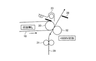
まず、2次転写ローラ32だけにバイアスを印加する場合について説明する。図2は、中間転写駆動ローラ20への印加バイアスは無し(0V)で、2次転写ローラ32への印加バイアスを「+6000V」とした例である。つまり、図2の例では、2次転写バイアスは、2次転写ローラ32にのみ印加されている。中間転写駆動ローラ20と2次転写ローラ32との電位差は、「6000V」である。
(Example of applied bias)
First, a case where a bias is applied only to the
紙などの媒体を伝った2次転写バイアスの放電を防止ないし低減するためには、2次転写ローラ32に印加する2次転写用バイアス(図2の例では、「+6000V」)を低減することが望ましい。そこで、本実施形態では、2次転写ローラ32に印加するバイアスを低減するとともに、低減した分に対応する逆極性のバイアスを中間転写駆動ローラ20に印加する。中間転写駆動ローラ20にもバイアスを印加する場合、上述のように、近傍の1次転写ローラ等に印加バイアスが放電するおそれが生じる。
In order to prevent or reduce the discharge of the secondary transfer bias transmitted through a medium such as paper, the secondary transfer bias (“+6000 V” in the example of FIG. 2) applied to the
例えば、画像形成装置1が小型である場合、中間転写駆動ローラ20と感光体16Bk等との距離が短い。このため、2次転写(転写ベルト10から媒体へのトナーの移動)に必要な電流値供給において、中間転写駆動ローラ20側に2次転写に必要な電流値を確保可能な電圧値を印加すると、近傍の1次転写ローラ24Bk等に印加バイアスが放電してしまう。
For example, when the image forming apparatus 1 is small, the distance between the intermediate
一方、ある一定の電圧値未満のバイアス値を印加すれば、そのような放電が生じないことが分かっている。そこで本実施形態では、このような放電が生じないバイアス値を求め、求めたバイアス値以下となるバイアスを中間転写駆動ローラ20に印加する。
On the other hand, it is known that such a discharge does not occur when a bias value less than a certain voltage value is applied. Therefore, in the present embodiment, a bias value that does not cause such discharge is obtained, and a bias that is equal to or less than the obtained bias value is applied to the intermediate
また、2次転写に必要な電流値を確保可能な電圧値は、転写ベルトと媒体との間の電位差である。中間転写駆動ローラ20にバイアスを印加すれば、印加した電圧値の分だけ、必要な電位差を得るために2次転写ローラ32に印加する電圧値を減らすことができる。これにより、紙などの媒体を伝った2次転写バイアスの放電を防止ないし低減することができる。
Further, the voltage value that can secure the current value necessary for the secondary transfer is a potential difference between the transfer belt and the medium. If a bias is applied to the intermediate
中間転写駆動ローラ20に印加するバイアス値の決定方法としては、1次転写ローラ24Bk等に放電しない、若しくは画像形成上許容される放電量となる電圧値を、事前に実験により求めておき、その電圧値に基づいてバイアス値を決める方法が考えられる。また、環境条件により、中間転写駆動ローラ20に印加するバイアス値を補正する方法も考えられる。環境条件は、例えば、温度、湿度、経年変化、および、気圧などである。
As a method for determining the bias value to be applied to the intermediate
なお、図2の例のように高電圧(例えば「+6000V」)を印加するためには、一般には封止タイプのトランスを使う必要がある。オープンタイプのトランスは、通常、比較的低電圧の印加にしか用いることができないためである。本実施形態では、中間転写駆動ローラ20と2次転写ローラ32との両方に逆極性のバイアスを印加するため、各ローラに印加するバイアス値を比較的小さい値とすることができる。これにより、オープンタイプのトランスを用いることができるようになる。
In order to apply a high voltage (for example, “+6000 V”) as in the example of FIG. 2, it is generally necessary to use a sealing type transformer. This is because an open-type transformer can usually be used only for applying a relatively low voltage. In the present embodiment, since a reverse polarity bias is applied to both the intermediate
図3は、2次転写バイアスを、中間転写駆動ローラ20と2次転写ローラ32との両方に印加する場合の例を示す図である。図3の例では、中間転写駆動ローラ20への印加バイアスは「−1200V」で、2次転写ローラ32への印加バイアスは「+4800V」である。この場合でも、中間転写駆動ローラ20と2次転写ローラ32との印加バイアスの差は、+4800−(−1200)=6000Vである。つまり、図3の例において、中間転写駆動ローラ20と2次転写ローラ32との電位差は、図2の場合と同じで「6000V」である。しかしながら、図3の例では、2次転写ローラ32への印加バイアス値は「4800V」であり、図2の場合に比べて印加バイアス値を「1200V」低減できる。
FIG. 3 is a diagram illustrating an example in which the secondary transfer bias is applied to both the intermediate
これにより、紙などの媒体を伝った2次転写バイアスの放電を防止ないし低減することができる。また図3の例では、印加バイアス「+4800V」を印加するためのトランスにはオープンタイプのトランスを用いることができる。また、印加バイアス「−1200V」を印加するためのトランスにもオープンタイプのトランスを用いることができる。 Thereby, it is possible to prevent or reduce the discharge of the secondary transfer bias transmitted through a medium such as paper. In the example of FIG. 3, an open type transformer can be used as a transformer for applying the applied bias “+4800 V”. An open type transformer can also be used as a transformer for applying the applied bias “−1200 V”.
このように、本実施形態では、2次転写ローラへの印加バイアス値を低減させることにより、画像形成装置1内の電源部41の規模を軽減できる。すなわち、紙などの媒体を伝った放電が減少することで、供給が必要な電流値を減らし、更に、中間転写駆動ローラ20と2次転写ローラ32との両方に印加することで1箇所への印加を軽減する。これにより、出力が小さなトランスを電源部41に使用することができる。特に、電源部41が備えるトランスのサイズを軽減することができる。例えば、印加バイアス値を絶対値で概ね「5000V」以下にすることができれば、小サイズかつ低コストのオープンタイプのトランスを使用することが可能になる。
Thus, in this embodiment, the scale of the
図3の例において、中間転写駆動ローラ20への印加バイアス及び2次転写ローラ32への印加バイアスについては、どちらか一方は印加電流値を一定に保つ構成を採用し、別の一方は印加電圧を一定に保つ構成を採用する。中間転写駆動ローラ20への印加バイアスについて、印加電圧を一定に保つ構成とすることにより、外部環境の変化に伴う抵抗値の変化に影響されにくい、1次転写ローラ24Bk等へ放電しない電圧値の制御が可能になる。つまり、中間転写駆動ローラ20から近傍の1次転写ローラ24Bk等へ印加バイアスが放電しない電圧値を、外部環境の変動による抵抗値変化に左右される事なしに設定することができる。
In the example of FIG. 3, for the applied bias to the intermediate
ところで、印加電圧を0Vに保つこととは接地(GNDに接続)するのと同じ意味である。一方の印加電圧値を一定に保ち、他方の印加電流値を一定に保つ構成では、印加電流値を一定に保つ側から見ると、印加電圧値を一定に保つ側は接地(GNDに接続)されているのと同じ関係になる。すなわち、一方に印加電流値を一定に保つバイアスを印加して、他方を接地もう片側を接地(GNDに接続)するのと同様である。これにより、2次転写ローラ32に印加する電圧を低減することができる。
By the way, maintaining the applied voltage at 0 V has the same meaning as grounding (connected to GND). In a configuration in which one applied voltage value is kept constant and the other applied current value is kept constant, when viewed from the side that keeps the applied current value constant, the side that keeps the applied voltage value constant is grounded (connected to GND). It becomes the same relationship as That is, it is the same as applying a bias that keeps the applied current value constant on one side and grounding the other side (connecting to GND) on the other side. Thereby, the voltage applied to the
図4は、2次転写バイアスを、中間転写駆動ローラ20と2次転写ローラ32との両方に印加する場合の例を示す図である。図4の例では、図3の例と同様に、中間転写駆動ローラ20への印加バイアスは「−1200V」で、2次転写ローラ32への印加バイアスは「+4800V」である。この場合でも、中間転写駆動ローラ20と2次転写ローラ32との印加バイアスの差は、+4800−(−1200)=6000Vである。
FIG. 4 is a diagram illustrating an example in which the secondary transfer bias is applied to both the intermediate
さらに、図4の例では、図3の例に加えて、除電部38である除電針にもバイアス電圧を印加する。この例では、中間転写駆動ローラ20への印加バイアスと同じ「−1200V」を除電部38に印加する。これにより、2次転写バイアスを2次転写ローラ32と中間転写駆動ローラ20との両方に印加する場合と、2次転写ローラ32のみに印加する場合とで、除電部38と2次転写ローラ32との間の電位差が同じになる。従って、2次転写ローラ32への印加バイアス値を下げた場合でも、除電効果を維持することができる。
Further, in the example of FIG. 4, in addition to the example of FIG. 3, a bias voltage is also applied to the static elimination needle as the
また、中間転写駆動ローラ20に印加するバイアス電圧のための配線(図示せず)から分岐させた配線により、同じバイアス電圧値を除電部38へ印加するようにしてもよい。こうすれば、別々の電源を用意する必要がない。
Further, the same bias voltage value may be applied to the
なお、図4の例では、除電部38へ印加するバイアス値は、中間転写駆動ローラ20に印加するバイアス値と同じ値としているが、必要に応じて異なるバイアス値を与えてもよい。
In the example of FIG. 4, the bias value applied to the
(バイアス印加部)
図5は、バイアス印加部42に含まれる、印加電圧値を一定に保つための定電圧回路の構成例を示す図である。図5の定電圧回路は、バイポーラトランジスタTrと、ツェナーダイオードDzと、抵抗Rとを備えている。図5において、負荷100は、例えば、図1から図4までの中間転写駆動ローラ20である。定電圧回路のプラス側入力端がバイポーラトランジスタTrのコレクタに、プラス側出力端がバイポーラトランジスタTrのエミッタに、それぞれ接続されている。定電圧回路のマイナス側入力端からプラス側入力端との間に、ツェナーダイオードDzおよび抵抗Rが直列に接続される。バイポーラトランジスタTrのベースは抵抗RとツェナーダイオードDzとの接続点に接続される。これにより、バイポーラトランジスタTrのベースがツェナー電圧Vzに保たれる。
(Bias application part)
FIG. 5 is a diagram illustrating a configuration example of a constant voltage circuit included in the bias applying unit 42 for keeping the applied voltage value constant. The constant voltage circuit of FIG. 5 includes a bipolar transistor Tr, a Zener diode Dz, and a resistor R. In FIG. 5, a
図5において、定電圧回路の出力電圧Voが低下すると、バイポーラトランジスタTrのベース・エミッタ間電圧VBEが増加して出力電流(コレクタ電流)が増加し、出力電圧Voが上昇する。一方、出力電圧Voが増加すると、バイポーラトランジスタTrのベース・エミッタ間電圧VBEが減少して出力電流(コレクタ電流)が減少し、出力電圧Voが降下する。このように動作するので、図5の定電圧回路は、常に出力電圧と逆の方向にフィードバック制御が働き、出力電圧を一定に保つことができる。 In FIG. 5, when the output voltage V o of the constant voltage circuit decreases, the base-emitter voltage V BE of the bipolar transistor Tr increases, the output current (collector current) increases, and the output voltage V o increases. On the other hand, when the output voltage V o increases, the base-emitter voltage V BE of the bipolar transistor Tr decreases, the output current (collector current) decreases, and the output voltage V o drops. Since it operates in this way, the constant voltage circuit of FIG. 5 can always maintain the output voltage constant by performing feedback control in the direction opposite to the output voltage.
図6は、バイアス印加部42に含まれる定電流回路の構成例を示す図である。図6の定電流回路は、バイポーラトランジスタTrと、ツェナーダイオードDzと、抵抗Rとを備えている。定電流回路のプラス側入力端がバイポーラトランジスタTrのベースに接続される。定電流回路のプラス側出力端がバイポーラトランジスタTrのコレクタに接続される。定電流回路のマイナス側入力端とプラス側入力端との間にツェナーダイオードDzが接続される。抵抗Rの一端はバイポーラトランジスタTrのエミッタに接続され、他端はマイナス側出力端に接続される。 FIG. 6 is a diagram illustrating a configuration example of a constant current circuit included in the bias applying unit 42. The constant current circuit of FIG. 6 includes a bipolar transistor Tr, a Zener diode Dz, and a resistor R. The positive side input terminal of the constant current circuit is connected to the base of the bipolar transistor Tr. The positive output terminal of the constant current circuit is connected to the collector of the bipolar transistor Tr. A zener diode Dz is connected between the negative side input terminal and the positive side input terminal of the constant current circuit. One end of the resistor R is connected to the emitter of the bipolar transistor Tr, and the other end is connected to the minus side output end.
図6のように、負荷100をバイポーラトランジスタTrのコレクタに繋ぐことによって、バイアス印加部42に含まれる定電流回路を実現できる。図6において、負荷100は、例えば、図1から図4までの2次転写ローラ32、又は、図4の除電部38である。図6において、バイポーラトランジスタTrのベース・エミッタ間電圧VBEは、ツェナーダイオードDzのツェナー電圧Vzによって一定に保たれるので、負荷100に流れる電流を一定に保つことができる。この定電流回路を用いることにより、負荷電圧が変動しても電流は変化しないので、負荷100に流れる電流を一定に保つことができる。
As shown in FIG. 6, the constant current circuit included in the bias applying unit 42 can be realized by connecting the
図7は、バイアス印加部42に含まれる、定電圧回路の他の構成例を示す図である。図7の定電圧回路は、バイポーラトランジスタTrと、ツェナーダイオードDzと、抵抗R1と、抵抗R2とを備えている。抵抗R1の一端は定電圧回路のプラス側入力端に接続され、他端はバイポーラトランジスタTrのエミッタに接続される。定電圧回路のマイナス側入力端からプラス側入力端との間に、ツェナーダイオードDzおよび抵抗R2が直列に接続される。バイポーラトランジスタTrのベースは抵抗R2とツェナーダイオードDzとの接続点に接続される。定電圧回路のプラス側出力端はバイポーラトランジスタTrのエミッタに接続され、マイナス側出力端はバイポーラトランジスタTrのコレクタに接続される。 FIG. 7 is a diagram illustrating another configuration example of the constant voltage circuit included in the bias applying unit 42. The constant voltage circuit of FIG. 7 includes a bipolar transistor Tr, a Zener diode Dz, a resistor R1, and a resistor R2. One end of the resistor R1 is connected to the positive side input terminal of the constant voltage circuit, and the other end is connected to the emitter of the bipolar transistor Tr. A Zener diode Dz and a resistor R2 are connected in series between the negative input end and the positive input end of the constant voltage circuit. The base of the bipolar transistor Tr is connected to the connection point between the resistor R2 and the Zener diode Dz. The positive output terminal of the constant voltage circuit is connected to the emitter of the bipolar transistor Tr, and the negative output terminal is connected to the collector of the bipolar transistor Tr.
図7の定電圧回路では、コレクタ・ベース間電圧VCBがツェナーダイオードDzのツェナー電圧Vzにより一定電圧に保たれている。図7において、負荷100は、例えば、図1から図4までの中間転写駆動ローラ20である。図7の定電圧回路において、出力電圧が増加するとコレクタ・エミッタ間電圧VCEが増加するが、コレクタ・ベース間電圧VCBはツェナーダイオードDzにより一定電圧に保たれているのでベース・エミッタ間電圧VBEが上昇し、コレクタ電流が増加する。これにより、抵抗R1による電圧降下が増加し、出力電圧の上昇を妨げる。一方、出力電圧が低下すると、コレクタ・エミッタ間電圧VCEが低下するが、コレクタ・ベース間電圧VCBはツェナーダイオードDzにより一定電圧に保たれているのでベース・エミッタ間電圧VBEが低下し、コレクタ電流が減少する。これにより、抵抗R1による電圧降下が減少し、出力電圧の低下を妨げる。
In the constant voltage circuit of FIG. 7, the collector-base voltage V CB is maintained at a constant voltage by the Zener voltage V z of the Zener diode Dz. In FIG. 7, a
以上のように、図7の定電圧回路によれば、常に出力電圧の変化しようとする方向と逆の方向にフィードバックが働き、出力電圧を一定に保つことができる。 As described above, according to the constant voltage circuit of FIG. 7, the feedback always works in the direction opposite to the direction in which the output voltage changes, and the output voltage can be kept constant.
図8は、バイアス印加部42において、誤差増幅器によるフィードバック用の回路を設けて、制御を行うことで、電圧を一定に保つ回路の例である。 FIG. 8 shows an example of a circuit that keeps the voltage constant by providing a feedback circuit using an error amplifier and performing control in the bias application unit 42.
図8の定電圧回路は、誤差増幅器43と、抵抗R1と、抵抗R2とを備えている。負荷100の一端から他端との間に、抵抗R1および抵抗R2が直列に接続される。誤差増幅器43の入力端の一方は抵抗R1と抵抗R2との接続点に接続される。誤差増幅器43の入力端の他方には基準電圧値Vrefが供給される。誤差増幅器43の出力は制御部40に入力される。制御部40は電源部41に接続され、誤差増幅器43の出力に応じて電源部41の出力値を制御する。
The constant voltage circuit of FIG. 8 includes an
図8において、負荷100は、例えば、図1から図4までの中間転写駆動ローラ20である。図8において、誤差増幅器43は、基準電圧値Vrefと、出力電圧Voを抵抗R1及びR2で分圧した電圧値VSとを比較する。誤差増幅器43は、検出される電圧値の誤差を制御部40にフィードバックする。制御部40は、基準電圧値Vrefと電圧値VSとが等しくなる様に、電源部41に出力を命令する。これにより、負荷100への出力電圧V0の値を一定に保つことができる。
In FIG. 8, a
図9は、バイアス印加部42において、誤差増幅器43によるフィードバック用の回路を設けて、制御を行うことで、電流を一定に保つ回路の例である。
FIG. 9 is an example of a circuit that keeps the current constant by providing a feedback circuit using the
図9の定電流回路は、誤差増幅器43と、電流検出抵抗RSとを備えている。負荷100の一端から他端との間に、制御部40、電源部41、および電流検出抵抗RSが直列に接続される。誤差増幅器43の入力端の一方は電流検出抵抗RSと負荷100との接続点に接続される。誤差増幅器43の入力端の他方には基準電圧値Vrefが供給される。誤差増幅器43の出力は制御部40に入力される。制御部40は、誤差増幅器43の出力に応じて電源部41の出力値を制御する。
The constant current circuit of FIG. 9 includes an
図9において、負荷100は、例えば、図1から図4までの2次転写ローラ32、又は、図4の除電部38である。図9において、誤差増幅器43は基準電圧値Vrefと、出力電流I0が電流検出抵抗RSを流れることで発生する電圧値VSとを比較する。誤差増幅器43は、検出される電圧値の誤差を制御部40にフィードバックする。制御部40は、基準電圧値Vrefと電圧値VSとが等しくなる様に、電源部41に出力を命令する。これにより、負荷100に流れる出力電流I0の値を一定に保つことができる。
In FIG. 9, a
上記の他、フィードバック用の回路を設けて制御を行う構成を採用し、電圧又は電流を一定に保つことができる。例えば、電源部41自体は電流を一定に保つ回路を持っていない場合でも、電源部41の外部に電圧又は電流を一定に保つフィードバック用の回路を設けて、制御を行うことで、出力電圧値又は出力電流値を一定に保つことができる。
In addition to the above, it is possible to maintain a constant voltage or current by adopting a configuration in which a feedback circuit is provided for control. For example, even when the
以下、トランスの例について説明する。扱う電圧が高いトランスについては、絶縁耐圧を保つための空間距離及び沿面距離を大きくする必要がある。封止タイプのトランスは、空間距離及び沿面距離の不足に対応するために、トランスと出力制御回路とを一体化して樹脂などによって封止したものである。封止タイプのトランスは、樹脂などの封止材によって固体絶縁が実現される。なお、扱う電圧が概ね4KVを超える場合、この封止タイプのトランスを使用することが多い。一般的には、扱う電圧が5KV以上の場合、ほとんどが封止タイプのトランスとなる。 Hereinafter, an example of a transformer will be described. For transformers that handle high voltages, it is necessary to increase the spatial distance and creepage distance to maintain the withstand voltage. In order to cope with the shortage of the spatial distance and the creepage distance, the sealing type transformer is obtained by integrating the transformer and the output control circuit and sealing with a resin or the like. In a sealing type transformer, solid insulation is realized by a sealing material such as resin. In addition, when the voltage to handle exceeds about 4KV, this sealing type transformer is often used. Generally, when the voltage to be handled is 5 KV or more, most of them are sealed type transformers.
オープンタイプのトランスは、封止材による固体絶縁に頼らないで、沿面距離及び空間距離を確保する構成のトランスである。オープンタイプのトランスは、封止タイプのトランスと比べて、小型、軽量化が図れる。また、部材、組み立て工数も少ないので、低価格でもある。 An open type transformer is a transformer configured to ensure a creepage distance and a spatial distance without relying on solid insulation by a sealing material. An open type transformer can be made smaller and lighter than a sealed type transformer. Moreover, since the number of members and assembly man-hours is small, the price is low.
(まとめ)
以上説明したように、本実施形態によれば、像担持体から1次転写ローラへ放電する電圧値未満のバイアスを中間転写駆動ローラに印加し、かつ、中間転写駆動ローラに印加するバイアスに応じた電圧値とは極性の異なるバイアスを2次転写ローラに印加することにより、紙などの媒体を伝った2次転写バイアスの放電を防止ないし低減できる。また、中間転写駆動ローラから1次転写ローラへ放電しない電圧値を知り、この電圧値未満の電圧を中間転写駆動ローラに印加し、片側の印加電圧値を一定に保ち、もう片側の印加電流値を一定に保つ構成とすることで、トナー移動に必要な電流値を確保しつつ、中間転写駆動ローラに印加した電圧値の分だけ2次転写ローラに印加しなければならない電圧値を減らすことができる。
(Summary)
As described above, according to this embodiment, a bias less than the voltage value for discharging from the image carrier to the primary transfer roller is applied to the intermediate transfer drive roller, and the bias is applied to the intermediate transfer drive roller. By applying a bias having a polarity different from the voltage value to the secondary transfer roller, discharge of the secondary transfer bias transmitted through a medium such as paper can be prevented or reduced. Also, know the voltage value that does not discharge from the intermediate transfer drive roller to the primary transfer roller, apply a voltage less than this voltage value to the intermediate transfer drive roller, keep the applied voltage value on one side constant, and the applied current value on the other side By keeping the current constant, it is possible to reduce the voltage value that must be applied to the secondary transfer roller by the amount of the voltage value applied to the intermediate transfer driving roller while securing the current value necessary for toner movement. it can.
なお、本発明は、複写機、プリンタ、スキャナ装置、ファクシミリ装置等の画像形成装置の他、コピー機能、プリンタ機能、スキャナ機能及びファクシミリ機能のうち少なくとも2つの機能を有する複合機に適用することができる。 The present invention can be applied to a multifunction machine having at least two of a copy function, a printer function, a scanner function, and a facsimile function, in addition to an image forming apparatus such as a copying machine, a printer, a scanner device, and a facsimile device. it can.
1 画像形成装置
10 転写ベルト
11Bk,11M,11C,11Y カートリッジ
12Bk,12M,12C,12Y パドル
13Bk,13M,13C,13Y 供給ローラ
14Bk,14M,14C,14Y 現像器
15Bk,15M,15C,15Y 現像ブレード
16Bk,16M,16C,16Y 感光体
17Bk,17M,17C,17Y 帯電器
18Bk,18M,18C,18Y クリーナーブレード
19 露光器
20 中間転写駆動ローラ
21 転写ベルトテンションローラ
22 トナーマークセンサ
23 転写ベルトクリーナ
24Bk,24M,24C,24Y 1次転写ローラ
25 給紙トレイ
26 用紙
27 廃トナーボックス
28 廃トナーフル検知センサ
29 給紙ローラ
30 センサ
31 レジストローラ
32 2次転写ローラ
33 定着器
34 排紙センサ
35 排紙ローラ
36 両面ローラ
37 両面センサ
38 除電部
39 通紙経路
40 制御部
41 電源部
42 バイアス印加部
43 誤差増幅器
100 負荷
1
Claims (5)
前記静電潜像にトナーを付着させることによって形成されるトナー画像が転写される像担持体と、
前記トナー画像を前記感光体から前記像担持体へ転写する1次転写ローラと、
前記トナー画像を前記像担持体から媒体に2次転写する2次転写ローラと、
前記像担持体から前記1次転写ローラへ放電する電圧値未満のバイアスを、前記像担持体を駆動する中間転写駆動ローラに印加し、かつ、前記中間転写駆動ローラに印加するバイアスとは極性が異なり該バイアスに応じた電圧値のバイアスを、前記2次転写ローラに印加することによって、前記2次転写に必要な電圧値である2次転写バイアスを印加するバイアス印加部と、
前記トナー画像が転写された媒体に該トナー画像を定着させる定着部と、
を備えたことを特徴とする画像形成装置。 A photoreceptor on which an electrostatic latent image is formed;
An image carrier to which a toner image formed by attaching toner to the electrostatic latent image is transferred;
A primary transfer roller for transferring the toner image from the photoreceptor to the image carrier;
A secondary transfer roller for secondary transfer of the toner image from the image carrier to a medium;
A bias less than a voltage value discharged from the image carrier to the primary transfer roller is applied to the intermediate transfer drive roller that drives the image carrier, and the bias applied to the intermediate transfer drive roller has a polarity. A bias applying unit that applies a secondary transfer bias that is a voltage value necessary for the secondary transfer by applying a bias having a voltage value corresponding to the bias to the secondary transfer roller,
A fixing unit for fixing the toner image on a medium onto which the toner image is transferred;
An image forming apparatus comprising:
前記バイアス印加部は、前記中間転写駆動ローラに印加するバイアスと同電位のバイアスを前記除電部に印加することを特徴とする請求項1又は2に記載の画像形成装置。 A static elimination unit for neutralizing the medium;
The image forming apparatus according to claim 1, wherein the bias applying unit applies a bias having the same potential as a bias applied to the intermediate transfer driving roller to the charge eliminating unit.
前記静電潜像にトナーを付着させてトナー画像を形成する工程と、
1次転写ローラにより、前記感光体から像担持体に、前記トナー画像を転写する工程と、
前記像担持体から前記1次転写ローラへ放電する電圧値未満のバイアスを中間転写駆動ローラに印加し、前記中間転写駆動ローラに印加するバイアスに応じた電圧値とは極性の異なるバイアスを2次転写ローラに印加することによって、2次転写に必要な電圧値である2次転写バイアスを印加する工程と、
前記2次転写ローラにより、前記像担持体から媒体に、前記トナー画像を2次転写する工程と、
を含むことを特徴とする画像形成方法。 Forming an electrostatic latent image on the photoreceptor;
Forming a toner image by attaching toner to the electrostatic latent image;
A step of transferring the toner image from the photosensitive member to an image carrier by a primary transfer roller;
A bias less than a voltage value for discharging from the image carrier to the primary transfer roller is applied to the intermediate transfer driving roller, and a bias having a polarity different from the voltage value corresponding to the bias applied to the intermediate transfer driving roller is secondary. Applying a secondary transfer bias, which is a voltage value necessary for secondary transfer, by applying to the transfer roller;
Secondary transfer of the toner image from the image carrier to a medium by the secondary transfer roller;
An image forming method comprising:
Priority Applications (2)
| Application Number | Priority Date | Filing Date | Title |
|---|---|---|---|
| JP2014007969A JP6241289B2 (en) | 2013-03-15 | 2014-01-20 | Image forming apparatus and image forming method |
| US14/208,131 US9128422B2 (en) | 2013-03-15 | 2014-03-13 | Image forming apparatus and image forming method |
Applications Claiming Priority (3)
| Application Number | Priority Date | Filing Date | Title |
|---|---|---|---|
| JP2013054435 | 2013-03-15 | ||
| JP2013054435 | 2013-03-15 | ||
| JP2014007969A JP6241289B2 (en) | 2013-03-15 | 2014-01-20 | Image forming apparatus and image forming method |
Publications (2)
| Publication Number | Publication Date |
|---|---|
| JP2014199426A true JP2014199426A (en) | 2014-10-23 |
| JP6241289B2 JP6241289B2 (en) | 2017-12-06 |
Family
ID=51527538
Family Applications (1)
| Application Number | Title | Priority Date | Filing Date |
|---|---|---|---|
| JP2014007969A Expired - Fee Related JP6241289B2 (en) | 2013-03-15 | 2014-01-20 | Image forming apparatus and image forming method |
Country Status (2)
| Country | Link |
|---|---|
| US (1) | US9128422B2 (en) |
| JP (1) | JP6241289B2 (en) |
Families Citing this family (3)
| Publication number | Priority date | Publication date | Assignee | Title |
|---|---|---|---|---|
| EP3246760A1 (en) | 2016-05-18 | 2017-11-22 | Canon Kabushiki Kaisha | Image forming apparatus |
| JP6729172B2 (en) * | 2016-08-24 | 2020-07-22 | コニカミノルタ株式会社 | Image forming apparatus and image forming method |
| JP2019219487A (en) | 2018-06-19 | 2019-12-26 | 株式会社リコー | Image forming device and image forming method |
Citations (5)
| Publication number | Priority date | Publication date | Assignee | Title |
|---|---|---|---|---|
| JPH0481153U (en) * | 1990-11-28 | 1992-07-15 | ||
| JP2006010882A (en) * | 2004-06-23 | 2006-01-12 | Ricoh Co Ltd | Color image forming apparatus |
| US20090060595A1 (en) * | 2007-09-05 | 2009-03-05 | Kyocera Mita Corporation | Image forming apparatus |
| JP2009122168A (en) * | 2007-11-12 | 2009-06-04 | Ricoh Co Ltd | Image forming apparatus and bias voltage application control method for image forming apparatus |
| JP2011007907A (en) * | 2009-06-24 | 2011-01-13 | Ricoh Co Ltd | Image forming apparatus |
Family Cites Families (11)
| Publication number | Priority date | Publication date | Assignee | Title |
|---|---|---|---|---|
| US4095206A (en) * | 1975-02-10 | 1978-06-13 | Victor Company Of Japan, Limited | Encapsulated transformer assembly |
| JP3592488B2 (en) | 1997-07-04 | 2004-11-24 | 株式会社リコー | Image forming device |
| JP2002318494A (en) | 2001-04-20 | 2002-10-31 | Fuji Xerox Co Ltd | Image forming device |
| JP2005331845A (en) * | 2004-05-21 | 2005-12-02 | Ricoh Printing Systems Ltd | Image forming system |
| JP2006156719A (en) | 2004-11-30 | 2006-06-15 | Matsushita Electric Ind Co Ltd | Component unit |
| JP4892932B2 (en) * | 2005-11-07 | 2012-03-07 | 富士ゼロックス株式会社 | Image forming apparatus |
| US8335462B2 (en) * | 2009-10-30 | 2012-12-18 | Kyocera Mita Corporation | Image forming apparatus |
| JP5900056B2 (en) * | 2011-06-08 | 2016-04-06 | 株式会社リコー | Image forming apparatus |
| JP5825875B2 (en) * | 2011-06-17 | 2015-12-02 | キヤノン株式会社 | Image forming apparatus |
| JP5891628B2 (en) * | 2011-07-15 | 2016-03-23 | 株式会社リコー | Image forming apparatus |
| JP5958274B2 (en) * | 2012-10-25 | 2016-07-27 | 富士ゼロックス株式会社 | Image forming apparatus |
-
2014
- 2014-01-20 JP JP2014007969A patent/JP6241289B2/en not_active Expired - Fee Related
- 2014-03-13 US US14/208,131 patent/US9128422B2/en not_active Expired - Fee Related
Patent Citations (5)
| Publication number | Priority date | Publication date | Assignee | Title |
|---|---|---|---|---|
| JPH0481153U (en) * | 1990-11-28 | 1992-07-15 | ||
| JP2006010882A (en) * | 2004-06-23 | 2006-01-12 | Ricoh Co Ltd | Color image forming apparatus |
| US20090060595A1 (en) * | 2007-09-05 | 2009-03-05 | Kyocera Mita Corporation | Image forming apparatus |
| JP2009122168A (en) * | 2007-11-12 | 2009-06-04 | Ricoh Co Ltd | Image forming apparatus and bias voltage application control method for image forming apparatus |
| JP2011007907A (en) * | 2009-06-24 | 2011-01-13 | Ricoh Co Ltd | Image forming apparatus |
Also Published As
| Publication number | Publication date |
|---|---|
| US9128422B2 (en) | 2015-09-08 |
| US20140270864A1 (en) | 2014-09-18 |
| JP6241289B2 (en) | 2017-12-06 |
Similar Documents
| Publication | Publication Date | Title |
|---|---|---|
| US9152070B2 (en) | Transfer device and image forming apparatus | |
| JP5884437B2 (en) | Optical writing apparatus, image forming apparatus, and control method for optical writing apparatus | |
| US9465348B2 (en) | Power supply device, image forming apparatus, and voltage output method | |
| JP2008224955A (en) | Image forming apparatus and image forming method | |
| JP2014109719A (en) | Optical writing control device, image forming apparatus and method for controlling optical writing device | |
| JP6241289B2 (en) | Image forming apparatus and image forming method | |
| JP5880023B2 (en) | Power supply circuit, image forming apparatus | |
| JP6201657B2 (en) | Image transfer control apparatus, image forming apparatus, and image transfer apparatus control method | |
| JP2017223874A (en) | Image forming apparatus | |
| JP2010048960A (en) | Image forming apparatus | |
| JP2008032807A (en) | Rotation body drive device and image forming apparatus | |
| JP6103189B2 (en) | Image forming apparatus | |
| JP2009122168A (en) | Image forming apparatus and bias voltage application control method for image forming apparatus | |
| US9946185B2 (en) | Image forming apparatus, and method and computer-readable medium for the same | |
| KR20110046255A (en) | Image Forming Device | |
| JP5089285B2 (en) | Color image forming apparatus | |
| US11934131B2 (en) | Image forming apparatus with a laser power correcting feature | |
| US20230113467A1 (en) | Image forming apparatus | |
| JP2006201383A (en) | Image forming apparatus | |
| JP2023173149A (en) | Image forming apparatus | |
| JP2016080976A (en) | Image forming apparatus and image forming method | |
| JP2015012773A (en) | High-voltage power supply unit and image formation device | |
| JP2006201384A (en) | Image forming apparatus | |
| JP2011164476A (en) | Image forming apparatus | |
| JP2014109734A (en) | Image forming apparatus and conveyance control method |
Legal Events
| Date | Code | Title | Description |
|---|---|---|---|
| A621 | Written request for application examination |
Free format text: JAPANESE INTERMEDIATE CODE: A621 Effective date: 20170110 |
|
| TRDD | Decision of grant or rejection written | ||
| A977 | Report on retrieval |
Free format text: JAPANESE INTERMEDIATE CODE: A971007 Effective date: 20170927 |
|
| A01 | Written decision to grant a patent or to grant a registration (utility model) |
Free format text: JAPANESE INTERMEDIATE CODE: A01 Effective date: 20171010 |
|
| A61 | First payment of annual fees (during grant procedure) |
Free format text: JAPANESE INTERMEDIATE CODE: A61 Effective date: 20171023 |
|
| R151 | Written notification of patent or utility model registration |
Ref document number: 6241289 Country of ref document: JP Free format text: JAPANESE INTERMEDIATE CODE: R151 |
|
| LAPS | Cancellation because of no payment of annual fees |