JP2014192259A - Double-sided wiring flexible substrate and inspection method thereof - Google Patents
Double-sided wiring flexible substrate and inspection method thereof Download PDFInfo
- Publication number
- JP2014192259A JP2014192259A JP2013065018A JP2013065018A JP2014192259A JP 2014192259 A JP2014192259 A JP 2014192259A JP 2013065018 A JP2013065018 A JP 2013065018A JP 2013065018 A JP2013065018 A JP 2013065018A JP 2014192259 A JP2014192259 A JP 2014192259A
- Authority
- JP
- Japan
- Prior art keywords
- double
- land portion
- sided wiring
- flexible substrate
- wiring flexible
- Prior art date
- Legal status (The legal status is an assumption and is not a legal conclusion. Google has not performed a legal analysis and makes no representation as to the accuracy of the status listed.)
- Pending
Links
Images


Landscapes
- Printing Elements For Providing Electric Connections Between Printed Circuits (AREA)
- Wire Bonding (AREA)
Abstract
Description
本発明は、両面配線フレキシブル基板及びその検査方法に関する。 The present invention relates to a double-sided wiring flexible substrate and an inspection method thereof.
従来から、液晶やEL(Electro Luminescence)等のディスプレイを駆動するためのIC(Integrated Circuit)チップ搭載用基板として、フレキシブル配線基板が用いられている。 Conventionally, a flexible wiring substrate has been used as a substrate for mounting an IC (Integrated Circuit) chip for driving a display such as liquid crystal or EL (Electro Luminescence).
ディスプレイの高精細化への要求が高まるに従い、それに用いられるフレキシブル配線基板も高機能・高密度化が求められている。かかる要請に応えるべく、種々の絶縁性基材の両面に配線を形成したフレキシブル配線基板(両面配線フレキシブル基板)が開発されてきている(例えば、特許文献1、2参照)。 As the demand for higher definition of displays increases, the flexible wiring board used therefor is also required to have higher functionality and higher density. In order to meet such demands, flexible wiring boards (double-sided wiring flexible boards) in which wiring is formed on both surfaces of various insulating base materials have been developed (for example, see Patent Documents 1 and 2).
例えば、特許文献1には、ポリイミドやポリエステル等からなるベース基材に貫通孔を設け、貫通孔部分にメッキ層を形成するとともに、ベース基材の駆動用ICチップ搭載面に駆動用ICと接続されるインナーリード部を形成し、駆動用ICチップ非搭載面に、液晶表示パネルに接続されるアウターリード部を形成したフレキシブル配線基板が記載されている。 For example, in Patent Document 1, a through-hole is provided in a base substrate made of polyimide, polyester, or the like, a plated layer is formed in the through-hole portion, and a driving IC is connected to a driving IC chip mounting surface of the base substrate. There is described a flexible wiring board in which an inner lead portion to be formed is formed and an outer lead portion connected to a liquid crystal display panel is formed on a surface where the driving IC chip is not mounted.
また、特許文献2には、絶縁フィルムから成る絶縁性基材の両面に銅箔を設け、その両面の所定位置を貫通するように絶縁性基材に所定数のスルーホールを形成し、銅箔をエッチングして配線パターンを形成した後、更に配線保護のために一方の面にカバーレイを貼り付けた後に、他方の面にソルダーレジストを塗布した両面配線フィルムキャリアが記載されている。 Further, in Patent Document 2, copper foil is provided on both sides of an insulating base made of an insulating film, and a predetermined number of through holes are formed in the insulating base so as to penetrate predetermined positions on both sides. A double-sided wiring film carrier is described in which a wiring pattern is formed by etching and then a cover lay is attached to one surface for wiring protection and then a solder resist is applied to the other surface.
これらの両面配線フレキシブル基板においては、基材がフィルム状であり、光が透過することから、両面配線フレキシブル基板が完成した後で、基板の片面から光をあて、その透過画像を検出することにより、配線の欠けや太り等の異常を検出する透過式外観検査が行われている。 In these double-sided wiring flexible boards, the base material is film-like and light is transmitted. Therefore, after the double-sided wiring flexible board is completed, light is applied from one side of the board and the transmission image is detected. In addition, a transparent appearance inspection is performed to detect abnormalities such as chipping or weighting of wiring.
しかしながら、従来の両面配線フレキシブル基板においては、スルーホールが形成されるランド部の形状及び大きさが両面で等しく形成され、両面のランド部に位置ずれが生じた場合、位置ずれの量が基準範囲内であっても、ランド部の位置ずれが配線の欠けとして誤検出されるという問題があった。 However, in the conventional double-sided wiring flexible board, the shape and size of the land part where the through hole is formed are formed equally on both sides, and the positional deviation amount is within the reference range when the land part on both sides is misaligned. Even within this, there was a problem that the misalignment of the land portion was erroneously detected as missing wiring.
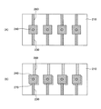
図1は、従来の両面配線フレキシブル基板のランド部を含む構成を示した図である。図1(A)は、従来の両面配線フレキシブル基板の断面図である。図1(A)において、絶縁性基材210にスルーホール250が形成され、スルーホール250内にはめっき層260が形成されるとともに、スルーホール250の上下の開口を塞ぐようにランド部240、270が形成されている。ここで、上面のランド部240と下面のランド部270とは、形状及び大きさが同じである。
FIG. 1 is a view showing a configuration including a land portion of a conventional double-sided wiring flexible substrate. FIG. 1A is a cross-sectional view of a conventional double-sided wiring flexible substrate. In FIG. 1A, a
図1(B)は、従来の両面配線フレキシブル基板の上面図である。図1(B)に示されるように、ランド部240は、めっき層260を含有するように形成されるとともに、配線パターン230が接続されている。また、ランド部240と反対面であり、ランド部240の下方にあるランド部270は、ランド部240と同一の形状及び大きさを有するため、上面視すると、ランド部240とランド部270とが重なり合い、ランド部270はランド部240に隠れた状態となる。また、ランド部270には、配線パターン280が接続されている。
FIG. 1B is a top view of a conventional double-sided wiring flexible substrate. As shown in FIG. 1B, the
図2は、従来の両面配線フレキシブル基板を透過式外観検査装置にて検査した際の光透過画像を示した図である。図2(A)は、両面配線フレキシブル基板の片面から光を当て、反対側から光透過画像を撮像した状態を示す図である。図2(A)に示されるように、配線の形成されていない絶縁性基材210は光を透過するため、光透過画像は白色画像を形成し、光を透過しない配線部パターン230、280は黒色画像を形成する。上面のランド部240と下面のランド部270とが一致して重なり合っていれば、図2(A)に示すように、ランド部240は1つに見える。
FIG. 2 is a view showing a light transmission image when a conventional double-sided wiring flexible board is inspected by a transmission type visual inspection apparatus. FIG. 2A is a diagram showing a state where light is applied from one side of the double-sided wiring flexible board and a light transmission image is taken from the opposite side. As shown in FIG. 2A, since the
一方、図2(B)は、両面のランド部に位置ずれが生じた場合の光透過画像を示した図である。従来の両面配線フレキシブル基板においては、スルーホール250が形成されるランド部240、270の形状及び大きさが同じであったため、両面のランド部240、270に位置ずれが生じた場合、透過式外観検査の透過画像が図2(B)のように検出される。このような透過画像が検出されたときに、実際には位置ずれの量が許容範囲内であっても、ランド部240、270の位置ずれが、配線の欠けとして誤検出され、歩留まりを低下させてしまうという問題があった。
On the other hand, FIG. 2B is a diagram showing a light transmission image in the case where a positional shift occurs in the land portions on both sides. In the conventional double-sided wiring flexible board, since the
そこで、本発明は、両面のランド部に位置ずれが生じた場合でも、位置ずれが許容範囲内であれば、透過式画像検査において誤検出が生じない構造の両面配線フレキシブル基板及びその検査方法を提供することを目的とする。 Therefore, the present invention provides a double-sided wiring flexible board having a structure that does not cause false detection in a transmission image inspection and a method for inspecting the same when the positional deviation is within an allowable range even when positional deviation occurs in both land portions. The purpose is to provide.
上記目的を達成するため、本発明の一態様に係る両面配線フレキシブル基板は、絶縁フィルムからなる絶縁性基材と、
該絶縁性基材を貫通するスルーホールと、
該スルーホールを含むように前記絶縁性基材の両面に形成された第1及び第2のランド部と、
前記第1及び第2のランド部の各々に接続された第1及び第2の配線パターンと、を有し、
前記第1のランド部が、前記第2のランド部よりも大きく、上面視で前記第2のランド部を包含する。
In order to achieve the above object, a double-sided wiring flexible substrate according to an aspect of the present invention includes an insulating base material made of an insulating film,
A through hole penetrating the insulating substrate;
First and second land portions formed on both surfaces of the insulating base so as to include the through holes;
First and second wiring patterns connected to each of the first and second land portions;
The first land portion is larger than the second land portion and includes the second land portion in a top view.
また、本発明の他の態様に係る両面配線フレキシブル基板の検査方法は、前記両面配線フレキシブル基板を、前記第1のランド部が上面となるように載置する工程と、
前記第1のランド部及び前記第2のランド部について、上面から透過式外観検査を行う工程と、を有する。
Moreover, the inspection method of the double-sided wiring flexible board according to another aspect of the present invention includes a step of placing the double-sided wiring flexible board such that the first land portion is an upper surface,
A step of performing a transmission visual inspection from the upper surface of the first land portion and the second land portion.
本発明によれば、透過式の投影画像検査において、ランド部の位置ずれによる配線欠け等の誤検出を防止することができる。 According to the present invention, in the transmission type projection image inspection, it is possible to prevent erroneous detection of a wiring defect or the like due to a land portion misalignment.
以下、図面を参照して、本発明を実施するための形態の説明を行う。 DESCRIPTION OF EMBODIMENTS Hereinafter, embodiments for carrying out the present invention will be described with reference to the drawings.
〔実施形態1〕
図3は、本発明の実施形態1に係る両面配線フレキシブル基板の一例の全体構成を示した上面図である。実施形態1に係る両面配線フレキシブル基板は、絶縁性基材10と、インナーリード部20と、上面配線パターン30と、上面ランド部40と、下面配線パターン80と、アウターリード部90とを備える。なお、インナーリード部20、上面配線パターン30、上面ランド部40、下面配線パターン80及びアウターリード部90は、複数形成されている。
Embodiment 1
FIG. 3 is a top view showing an overall configuration of an example of the double-sided wiring flexible substrate according to Embodiment 1 of the present invention. The double-sided wiring flexible substrate according to the first embodiment includes an insulating
両面配線フレキシブル基板は、インナーリード部20、上面配線パターン30及び上面ランド部40が形成された上面に半導体チップ(図示せず)が搭載されて用いられる。よって、上面が半導体チップ搭載面であり、下面が半導体チップ非搭載面である。なお、両面配線フレキシブル基板に搭載される半導体チップは、用途に応じて種々の半導体チップであってよいが、例えば、液晶表示パネル等のディスプレイを駆動するための駆動用ICチップであってもよい。駆動用ICチップには、ディスプレイの駆動回路が搭載される。
The double-sided wiring flexible substrate is used with a semiconductor chip (not shown) mounted on the upper surface on which the
図3において、ポリイミド等からなる絶縁性基材10の一面に、上面配線パターン30として、所定ピッチに形成された複数本の導体が絶縁性基材10の幅方向に並列に形成されている。そして、導体の一端部が、駆動用ICチップの電極(図示せず)が接続されるインナーリード部20として用いられている。インナーリード部20は、上面配線パターン30に接続され、上面配線パターン30は、ランド部40に接続されている。
In FIG. 3, a plurality of conductors formed at a predetermined pitch are formed in parallel in the width direction of the insulating
一方、駆動用ICチップ非搭載面側に下面配線パターン80が形成され、この下面配線パターン80の一端部は、液晶表示パネルの電極端子部と接続されるアウターリード部90とされる。また、駆動用ICチップ搭載面側の上面配線パターン30と、非搭載面側の下面配線パターン80とは、ランド部40の下部のスルーホール(図3では図示せず)内に形成されためっき層により、電気的に接続されている。
On the other hand, a lower
このように、実施形態1に係る両面配線フレキシブル基板は、上面配線パターン30及び下面配線パターン80が両面の各々に形成され、両者がランド部40でスルーホールを介して接続されるとともに、上面配線パターン30がインナーリード部20を介して駆動用ICに接続され、下面配線パターン80がアウターリード部90を介してディスプレイの電極端子部と接続された構成を有する。
As described above, in the double-sided wiring flexible board according to the first embodiment, the upper
なお、個々の構成要素についてより詳細に説明すると、絶縁性基材10は、絶縁性フィルムからなる基材であり、柔軟で折り曲げ可能な材料から構成される。例えば、絶縁性基材10は、ポリイミド、ポリアミド、ポリエチレンテレフタレート(PET)、液晶ポリマー(LCP)等の材料を適宜用いて構成される。
The individual constituent elements will be described in more detail. The insulating
インナーリード部20は、半導体チップの端子が接続される部分である。半導体チップとインナーリード部20とは、例えば、半導体チップ上の接続端子とバンプ等により接続される。
The
上面配線パターン30は、インナーリード部20からの電気的接続を、各端子間の間隔を広げつつ外側に引き出すための配線である。
The upper
上面ランド部40は、絶縁性基材10の上面に形成された上面配線パターン30からの電気的接続を、下面(裏面)に導くための端子であり、下方に形成されるスルーホールと上面配線パターン30との電気的接続を行う。よって、上面ランド部40は、上面配線パターン30が接続されるとともに、スルーホールを含むように形成される。
The upper
なお、インナーリード部20、上面配線パターン30及び上面ランド部40は、種々の導体からなる金属配線材料で構成されてよいが、例えば、銅が用いられてもよい。例えば、銅めっきにより絶縁性基材10上に銅めっき層を形成し、これによりインナーリード部20、上面配線パターン30及び上面ランド部40を構成してもよい。
In addition, although the inner
また、インナーリード部20は、上面配線パターン30の半導体チップ側の端部であり、ランド部40は、上面配線パターン30のアウターリード部90側の端部であるので、上面配線パターン30の一部がインナーリード部20及びランド部40を構成していると考えてもよい。
Further, since the
下面配線パターン80は、絶縁性基材10の半導体チップ非搭載側の面に形成される配線パターンであり、アウターリード部90は、下面配線パターン80の外側の端部に形成された端子である。下面配線パターン80及びアウターリード部90も、上面配線パターン30及びインナーリード部20と同様の材料から構成され、それらと同様の構成を有してよいので、その説明を省略する。
The lower
図4は、図3のA部の拡大図である。図4(A)は、ランド部及びスルーホールの断面図であり、図4(B)は、A部の上面図である。 FIG. 4 is an enlarged view of a portion A in FIG. 4A is a cross-sectional view of the land portion and the through hole, and FIG. 4B is a top view of the A portion.
図4(A)において、絶縁性基材10及び上面ランド部40の他、スルーホール50、めっき層60及び下面ランド部70が複数示されている。スルーホール50は、絶縁性基材10を貫通する貫通孔として構成され、スルーホール50内には、めっき層60が形成されてスルーホール50を充填している。スルーホール50の上面の開口部52の上方には、上面ランド部40が形成され、スルーホール50の下面の開口部53の下方には、下面ランド部70が形成されている。下面ランド部70は、上面ランド部40と同様に金属配線材料で構成されており、めっき層60も金属配線材料で構成されているため、上面ランド部40と下面ランド部70との電気的接続が、めっき層60が内部に充填形成されたスルーホール50を介してなされている。なお、めっき層60及び下面ランド部70も、導体からなる種々の金属配線材料で構成されてよいが、例えば、ともに銅めっき層で構成されてもよい。
In FIG. 4A, in addition to the insulating
ここで、上面ランド部40は、下面ランド部70よりも大きく構成されており、下面ランド部40を覆い隠すように構成されている。つまり、両面配線フレキシブル基板を上面視したときに、上面ランド部40が下面ランド部70を包含し、下面ランド部70を覆い隠すような構成となっている。上述のように、上面ランド部40と下面ランド部70とは、めっき層60が充填形成されたスルーホール50を介して電気的に接続されているので、両者とも、スルーホール50を包含する位置に形成される。よって、上面ランド部40の大きさを下面ランド部70よりも大きく構成すれば、上面ランド部40が下面ランド部70を包含する構成とすることができる。このような構成とすれば、上面ランド部40と下面ランド部70との間に多少の位置ずれが発生したとしても、その位置ずれが上面ランド部40と下面ランド部70との大きさの相違の範囲内にあれば、下面ランド部70は、上面ランド部40に包含された状態にあり、上面ランド部40よりも外側にはみ出さないことになる。そうすると、透過式外観検査を行った場合に、図2(B)で説明したような、誤検査を防止することができる。
Here, the upper
図4(B)に示すように、両面配線フレキシブル基板を上面視したときに、下面ランド部70は、上面ランド部40に包含され、上面ランド部40に覆われた状態となる。また、上面ランド部40は、下面ランド部70に対して、若干のマージンを有して下面ランド部70を包含している。この状態で透過式外観検査を行えば、上面ランド部40と下面ランド部70との間に若干の位置ずれが発生したとしても、マージンの範囲内の位置ずれであれば、上面ランド部40が下面ランド部70を覆った状態は保たれる。よって、透過式外観検査の際、下面ランド部70は、上面ランド部40からはみ出さず、配線の欠けが発生しているとの誤検出を防止することができる。
As shown in FIG. 4B, when the double-sided wiring flexible substrate is viewed from above, the lower
一方、上面ランド部40のマージンの範囲を超えた位置ずれが発生している場合には、そのような位置ずれを検出することができる。よって、上面ランド部40と下面ランド部70との大きさの差、つまり上面ランド部40のマージンを適切に設定することにより、位置ずれの許容範囲内で、適切に位置ずれの誤検出を防止することができる。
On the other hand, when a positional deviation exceeding the margin range of the upper
このように、本実施形態に係る両面配線フレキシブル基板によれば、透過式外観検査の際、上面ランド部40と下面ランド部70との位置ずれに起因する配線の欠けの誤検出を防止することができる。また、上面ランド部40と下面ランド部70との大きさの差を適切に設定することにより、許容範囲外の位置ずれについては、適切に不良検出を行うことができる。
As described above, according to the double-sided wiring flexible board according to the present embodiment, it is possible to prevent erroneous detection of a chipping of the wiring due to the positional deviation between the upper
なお、透過式外観検査の際には、まず、本実施形態に係る両面配線フレキシブル基板を、面積が大きい上面ランド部40が上面となるように配置する。次いで、配置した両面配線フレキシブル基板の上面から透過式外観検査を行うようにする。このような透過式外観検査方法を行うことにより、上面ランド部40と下面ランド部70との位置ずれに起因する配線の欠けの誤検出を防止しつつ、適切に両面配線フレキシブル基板の外観検査を行うことができ、歩留まりを向上させることができる。
In the transmission appearance inspection, first, the double-sided wiring flexible substrate according to the present embodiment is arranged so that the upper
〔実施形態2〕
図5は、本発明の実施形態2に係る両面配線フレキシブル基板の一例を示した図である。実施形態2に係る両面配線フレキシブル基板は、スルーホールの構成のみが異なっており、全体構成については、実施形態1の図3と同様である。よって、実施形態2に係る両面配線フレキシブル基板については、実施形態1と異なる部分についてのみ説明を行う。そのため、図5においては、図3のA部の拡大図を示している。
[Embodiment 2]
FIG. 5 is a view showing an example of a double-sided wiring flexible board according to Embodiment 2 of the present invention. The double-sided wiring flexible substrate according to the second embodiment is different only in the configuration of the through holes, and the overall configuration is the same as that of FIG. 3 of the first embodiment. Therefore, the double-sided wiring flexible substrate according to the second embodiment will be described only for the parts different from the first embodiment. Therefore, in FIG. 5, the enlarged view of the A section of FIG. 3 is shown.
図5(A)は、実施形態2に係る両面配線フレキシブル基板の一例のランド部及びスルーホールの断面構成図である。図5(A)において、絶縁性基材10をスルーホール53が貫通し、スルーホール53内にめっき層61が充填形成され、スルーホール51の上面の開口部54を上面ランド部40が覆い、下面の開口部55を下方から下面ランド部70が覆っている点は、実施形態1に係る両面配線フレキシブル基板と同様である。また、上面ランド部40が、下面ランド部70よりも大きく形成され、下面ランド部70を包含するように形成されている点も、実施形態1に係る両面配線フレキシブル基板と同様である。
FIG. 5A is a cross-sectional configuration diagram of a land portion and a through hole as an example of the double-sided wiring flexible substrate according to the second embodiment. In FIG. 5A, the through
しかしながら、実施形態2に係る両面配線フレキシブル基板においては、スルーホール53が、上面の開口部54と下面の開口部55とで異なる開口幅又は開口径を有し、テーパー状の傾斜面を有して構成されている点で、実施形態1に係る両面配線フレキシブル基板と異なっている。上面ランド部40は、下面ランド部70よりも大きいため、実施形態2に係る両面配線フレキシブル基板においては、上面ランド部40及び下面ランド部70の大きさに対応させ、スルーホール53の上面の開口部54の開口径を、下面の開口部55の開口径よりも大きくして形成している。これにより、スルーホール53の側面は、テーパー状の傾斜面を形成し、より多くのめっき層61を充填でき、スルーホール53内の導電性を高めることができる。また、めっき処理の際、上面の開口部54が広くなっているので、スルーホール53内にめっき層61が充填し易くなり、めっき層61のスルーホール53内での充填形成を容易にすることができる。
However, in the double-sided wiring flexible board according to the second embodiment, the through
このように、実施形態2に係る両面配線フレキシブル基板においては、上面ランド部40の面積が大きくなったことを利用し、これに対応させてスルーホール53の上面の開口部54の開口径を大きくすることにより、両面配線フレキシブル基板の電気的特性と加工性を向上させることができる。
As described above, in the double-sided wiring flexible board according to the second embodiment, by utilizing the fact that the area of the upper
図5(B)は、実施形態2に係る両面配線フレキシブル基板の一例のランド部及びスルーホールの上面図である。上面ランド部40と下面ランド部70との関係は、実施形態1と同様であるが、実施形態1よりも、スルーホール53の上面の開口部54が大きくなっていることが示されている。これにより、導通性及びめっき加工性を向上させることができる。
FIG. 5B is a top view of a land portion and a through hole as an example of the double-sided wiring flexible substrate according to the second embodiment. Although the relationship between the upper
図6は、図5(A)のB部の拡大図である。図6に示すように、スルーホール53の傾斜角θは、用途に応じて種々の角度としてよい。スルーホール53の傾斜角θは、例えば、25°〜35°の範囲に設定することができるが、かかる設定角度は、加工法によっても異なる。この点は、後述する。
FIG. 6 is an enlarged view of a portion B in FIG. As shown in FIG. 6, the inclination angle θ of the through
また、実施形態2に係る両面配線フレキシブル基板の透過式外観検査方法は、実施形態1に係る両面配線フレキシブル基板の透過式外観検査方法と同様の方法で行うことができるので、その説明を省略する。 Moreover, since the transmission type visual inspection method for the double-sided wiring flexible substrate according to the second embodiment can be performed in the same manner as the transmission type visual inspection method for the double-sided wiring flexible substrate according to the first embodiment, the description thereof is omitted. .
次に、本発明の実施形態2に係る両面配線フレキシブル基板の製造方法について説明する。なお、今まで説明した構成要素には、同一の参照符号を付してその説明を省略する。 Next, a method for manufacturing a double-sided wiring flexible substrate according to Embodiment 2 of the present invention will be described. It should be noted that the constituent elements described so far are denoted by the same reference numerals and description thereof is omitted.
最初に、絶縁性基材10の両面に銅箔を有するテープを用意する。これは絶縁フィルムの両面に接着剤層なしで銅層を設けたテープ又は少量の接着剤層を介して銅層を設けたテープのいずれでも良いが。高密度な配線パターンを形成するためには接着剤層を用いず、絶縁性基材10上にNi、Cr等のシード層を形成し、続けてCu層を形成した基板を用いることが好ましく、Cu層の厚みが薄い方が配線パターンの高密度化にはより好ましい。
First, a tape having copper foil on both surfaces of the insulating
絶縁性基材10としては、ポリイミド、ポリアミド、ポリエチレンテレフタレート(PET)、液晶ポリマー(LCP)等を適宜用いることができる。
As the insulating
次にスルーホール53を形成した後に、両面銅箔の導通を得るために銅めっきを施して、銅めっきを施した銅層と、銅めっきを施して、銅めっき層61により導通化したスルーホール53とを形成する。
Next, after forming the through
スルーホール53の形成は金型による打抜き法、エッチング法、レーザー法等の公知のスルーホール形成法を用いることができるが、本実施形態では、下面ランド部70を対向する上面ランド部40より小さくする。よって、小さな下面ランド部70には、小径のスルーホール開口部55を対応して形成するため、エッチング法又はレーザー法によりスルーホール53を形成することが望ましい。
The through-
図6に、スルーホール53の傾斜角θを示しているが、エッチング法の場合はスルーホールの傾斜角θが約25°乃至35°で形成され、レーザー法の場合は前記傾斜角が5°乃至15°で形成することができる。よって、配線幅や配線間隔、絶縁性基材の厚み、形成したいスルーホール径を考慮し、適宜、所望の加工方法を選択することができる。
6 shows the inclination angle θ of the through
更に、フォトレジストを用いたエッチング法にて、ランド部40、70及び配線パターン20、30、80、90を形成する。配線パターン形成は、公知のドライフィルムレジストの貼り付け、露光、現像、エッチング、剥膜の各工程を経て形成する。
Further, the
エッチング法における露光の際に、両面のレジストパターン形成の位置精度を考慮し、下面ランド部70の大きさを、レジストパターン形成の位置ずれの最大値よりも小さくする。ランド部40、70の大きさの設定は、あらかじめレジストパターン形成時に用いるフォトマスクに形成する露光パターンによって設定することによって本実施形態に係る両面配線フレキシブル基板ができる。
At the time of exposure in the etching method, considering the positional accuracy of resist pattern formation on both sides, the size of the lower
なお、本実施形態に係る両面配線フレキシブル基板の製造方法は、これに限定されることなく、例えば、ランド部40、70及び配線パターン20、30、80、90の形成をエッチング法以外にめっき法によって形成することもできる。
In addition, the manufacturing method of the double-sided wiring flexible substrate which concerns on this embodiment is not limited to this, For example, the formation of the
また、実施形態1に係る両面配線フレキシブル基板は、スルーホール50の形成を、傾斜を設けずに行えばよく、加工法としては、実施形態2と同様の方法であってよい。また、その他の構成要素については、実施形態2に係る両面配線フレキシブル基板の製造方法をそのまま適用することができる。
In the double-sided wiring flexible substrate according to the first embodiment, the through
〔実施形態3〕
図7は、本発明の実施形態3に係る両面配線フレキシブル基板の一例を示した図である。実施形態3に係る両面フレキシブル基板は、実施形態1、2に係る両面配線フレキシブル基板を、ディスプレイに実装した例について説明する。
[Embodiment 3]
FIG. 7 is a view showing an example of a double-sided wiring flexible board according to Embodiment 3 of the present invention. The double-sided flexible substrate according to the third embodiment will be described with respect to an example in which the double-sided wiring flexible substrate according to the first and second embodiments is mounted on a display.
図7に、実施形態1、2に係る両面配線フレキシブル基板をディスプレイに実装した状態を示す。ディスプレイパネル110上に形成された回路140に設けられた接続端子(図示せず)と、両面配線フレキシブル基板の配線パターン80の一端に設けられたアウターリード部90が接続され、プリント配線板120上に設けられた接続端子130と、両面配線フレキシブル基板の配線パターン30とを接続する。両面配線フレキシブル基板のインナーリード部20は、駆動用ICチップ100の電極と接続されている。
FIG. 7 shows a state where the double-sided wiring flexible substrate according to the first and second embodiments is mounted on a display. A connection terminal (not shown) provided on the
このように、実施形態1、2に係る両面配線フレキシブル基板は、ディスプレイに適切に搭載して用いることができる。 Thus, the double-sided wiring flexible substrate according to Embodiments 1 and 2 can be appropriately mounted on a display and used.
〔実施例〕
実施例として、図4に記載した、実施形態1に係る両面配線フレキシブル基板を製造した。
〔Example〕
As an example, the double-sided wiring flexible substrate according to Embodiment 1 shown in FIG. 4 was manufactured.
まず、25μm厚のポリイミドフィルムの両面に0.5μmの銅層を形成したテープを用い、片面からUV−YAGレーザー(AOV社LSY−3355)を用いて上面側開口部径が20μmとなるようにスルーホールを形成した。その際のスルーホール下面側開口部径は10μmであった。 First, using a tape in which a 0.5 μm copper layer is formed on both sides of a 25 μm thick polyimide film, and using a UV-YAG laser (AOV LSY-3355) from one side, the upper surface side opening diameter is 20 μm. A through hole was formed. At that time, the diameter of the opening on the lower surface side of the through hole was 10 μm.
次に公知のデスミア処理後、スルーホール部にスパッタ法にて0.3μmの銅層を形成した。 Next, after a known desmear treatment, a 0.3 μm copper layer was formed in the through hole portion by sputtering.
次いで、回路配線パターンを形成するため、ドライフィルムを両面にラミネートした後、露光によりドライフィルムを感光し、現像により光の照射されていない部位のドライフィルムを除去し、めっき法によりドライフィルムの除去された部位に銅層を形成し、剥膜工程で残ったドライフィルムを除去し、配線幅10μ、上面のランド部100μm□、下面のランド部60μmの両面配線パターンを形成し、本実施例に係る両面配線フレキシブル基板を得た。 Next, in order to form a circuit wiring pattern, after laminating the dry film on both sides, the dry film is exposed by exposure, the dry film not exposed to light is removed by development, and the dry film is removed by plating. A copper layer is formed on the formed portion, the dry film remaining in the film removal step is removed, and a double-sided wiring pattern having a wiring width of 10 μm, an upper surface land portion of 100 μm □, and a lower surface land portion of 60 μm is formed. Such a double-sided wiring flexible substrate was obtained.
以上の条件にて製作した両面配線基板1000ピースを透過式外観検査装置で検査したところ、ランド部の位置ずれによる配線不良としての誤検出発生は0ピースであった。 When 1000 pieces of the double-sided wiring board manufactured under the above conditions were inspected with a transmission type visual inspection apparatus, the number of erroneous detections as a wiring failure due to the misalignment of the land portion was 0 pieces.
このように、本実施例に係る両面配線基板によれば、透過式外観検査における誤検出を確実に防止することができた。 Thus, according to the double-sided wiring board according to the present example, it was possible to reliably prevent erroneous detection in the transmission visual inspection.
以上、本発明の好ましい実施形態及び実施例について詳説したが、本発明は、上述した実施形態及び実施例に制限されることはなく、本発明の範囲を逸脱することなく、上述した実施形態及び実施例に種々の変形及び置換を加えることができる。 The preferred embodiments and examples of the present invention have been described in detail above. However, the present invention is not limited to the above-described embodiments and examples, and the above-described embodiments and examples can be performed without departing from the scope of the present invention. Various modifications and substitutions can be made to the embodiments.
10 絶縁性基材
20 インナーリード部
30、80 配線パターン
40、70 ランド部
50、53 スルーホール
51、52、54、55 開口部
60、61 めっき層
90 アウターリード部
DESCRIPTION OF
Claims (12)
該絶縁性基材を貫通するスルーホールと、
該スルーホールを含むように前記絶縁性基材の両面に形成された第1及び第2のランド部と、
前記第1及び第2のランド部の各々に接続された第1及び第2の配線パターンと、を有し、
前記第1のランド部が、前記第2のランド部よりも大きく、上面視で前記第2のランド部を包含する両面配線フレキシブル基板。 An insulating substrate made of an insulating film;
A through hole penetrating the insulating substrate;
First and second land portions formed on both surfaces of the insulating base so as to include the through holes;
First and second wiring patterns connected to each of the first and second land portions;
The double-sided wiring flexible substrate, wherein the first land portion is larger than the second land portion and includes the second land portion in a top view.
前記第1のランド部及び前記第2のランド部について、上面から透過式外観検査を行う工程と、を有する両面配線フレキシブル基板の検査方法。 Placing the double-sided wiring flexible substrate according to any one of claims 1 to 11 so that the first land portion is an upper surface;
A method for inspecting a flexible double-sided wiring board, comprising: a step of performing a transmissive appearance inspection from an upper surface of the first land portion and the second land portion.
Priority Applications (1)
| Application Number | Priority Date | Filing Date | Title |
|---|---|---|---|
| JP2013065018A JP2014192259A (en) | 2013-03-26 | 2013-03-26 | Double-sided wiring flexible substrate and inspection method thereof |
Applications Claiming Priority (1)
| Application Number | Priority Date | Filing Date | Title |
|---|---|---|---|
| JP2013065018A JP2014192259A (en) | 2013-03-26 | 2013-03-26 | Double-sided wiring flexible substrate and inspection method thereof |
Publications (1)
| Publication Number | Publication Date |
|---|---|
| JP2014192259A true JP2014192259A (en) | 2014-10-06 |
Family
ID=51838273
Family Applications (1)
| Application Number | Title | Priority Date | Filing Date |
|---|---|---|---|
| JP2013065018A Pending JP2014192259A (en) | 2013-03-26 | 2013-03-26 | Double-sided wiring flexible substrate and inspection method thereof |
Country Status (1)
| Country | Link |
|---|---|
| JP (1) | JP2014192259A (en) |
Cited By (2)
| Publication number | Priority date | Publication date | Assignee | Title |
|---|---|---|---|---|
| JP2017175085A (en) * | 2016-03-25 | 2017-09-28 | 住友金属鉱山株式会社 | Double-sided wiring flexible substrate |
| CN111463536A (en) * | 2020-04-08 | 2020-07-28 | 上海航天电子通讯设备研究所 | Manufacturing method of micro-coaxial circuit based on L CP flexible substrate and micro-coaxial circuit |
-
2013
- 2013-03-26 JP JP2013065018A patent/JP2014192259A/en active Pending
Cited By (2)
| Publication number | Priority date | Publication date | Assignee | Title |
|---|---|---|---|---|
| JP2017175085A (en) * | 2016-03-25 | 2017-09-28 | 住友金属鉱山株式会社 | Double-sided wiring flexible substrate |
| CN111463536A (en) * | 2020-04-08 | 2020-07-28 | 上海航天电子通讯设备研究所 | Manufacturing method of micro-coaxial circuit based on L CP flexible substrate and micro-coaxial circuit |
Similar Documents
| Publication | Publication Date | Title |
|---|---|---|
| US9295150B2 (en) | Method for manufacturing a printed circuit board | |
| US20090283301A1 (en) | Multilayer wiring board and method for manufacturing the same | |
| CN104349575B (en) | Flexible PCB and preparation method thereof | |
| JP2009260186A (en) | Multilayer flexible printed wiring board, and its method for manufacturing | |
| CN109769344B (en) | Circuit board and manufacturing method thereof | |
| KR20150102504A (en) | Embedded board and method of manufacturing the same | |
| US9859221B2 (en) | Multilayer wiring board with built-in electronic component | |
| TWI442861B (en) | Multilayer printed circuit board and method for manufacturing same | |
| CN103702509B (en) | Step-like wiring board and preparation method thereof | |
| JP2014229895A (en) | Printed circuit board and method of manufacturing printed circuit board | |
| JP2007220729A (en) | Wiring circuit board and manufacturing method thereof | |
| CN107645855B (en) | Leadless electroplating circuit board and manufacturing method thereof | |
| JP2017175085A (en) | Double-sided wiring flexible substrate | |
| KR20160019297A (en) | Printed circuit board and manufacturing method thereof | |
| US9814135B2 (en) | Printed wiring board and method for manufacturing the same | |
| TW201417644A (en) | Multi-layer printed circuit board and method for making the same | |
| JP2014192259A (en) | Double-sided wiring flexible substrate and inspection method thereof | |
| KR100891531B1 (en) | Device for detecting alignment error of pattern | |
| TWI511634B (en) | Method for manufacturing circuit board | |
| TWI511628B (en) | Package circuit board, method for manufactuing same and package structure | |
| TWI636720B (en) | Circuit board structure and method for fabricating the same | |
| TWI415531B (en) | Method for manufacturing printed circuit board | |
| KR100498977B1 (en) | Method of plating the conductive layer on the wall of the cavity in E-BGA PCB | |
| US20220336230A1 (en) | Interposer, manufacturing method therefor, and circuit board assembly | |
| TW201803417A (en) | Printed circuit board and mthod for manufacturing same |