JP2014187825A5 - - Google Patents
Download PDFInfo
- Publication number
- JP2014187825A5 JP2014187825A5 JP2013061425A JP2013061425A JP2014187825A5 JP 2014187825 A5 JP2014187825 A5 JP 2014187825A5 JP 2013061425 A JP2013061425 A JP 2013061425A JP 2013061425 A JP2013061425 A JP 2013061425A JP 2014187825 A5 JP2014187825 A5 JP 2014187825A5
- Authority
- JP
- Japan
- Prior art keywords
- negative potential
- switching element
- capacitor
- voltage
- semiconductor device
- Prior art date
- Legal status (The legal status is an assumption and is not a legal conclusion. Google has not performed a legal analysis and makes no representation as to the accuracy of the status listed.)
- Granted
Links
- 239000003990 capacitor Substances 0.000 claims description 33
- 239000004065 semiconductor Substances 0.000 claims description 20
- 238000010586 diagram Methods 0.000 description 20
- 229910021320 cobalt-lanthanum-strontium oxide Inorganic materials 0.000 description 5
- CZECQDPEMSVPDH-MNXVOIDGSA-N (3S)-3-amino-4-[[(2S)-1-[[(2S)-1-[[(1S)-1-carboxy-2-hydroxyethyl]amino]-3-methyl-1-oxobutan-2-yl]amino]-4-methyl-1-oxopentan-2-yl]amino]-4-oxobutanoic acid Chemical compound OC(=O)C[C@H](N)C(=O)N[C@@H](CC(C)C)C(=O)N[C@@H](C(C)C)C(=O)N[C@@H](CO)C(O)=O CZECQDPEMSVPDH-MNXVOIDGSA-N 0.000 description 4
- 230000000694 effects Effects 0.000 description 2
- 230000015556 catabolic process Effects 0.000 description 1
- 230000003334 potential Effects 0.000 description 1
Images


Description
ブートストラップ回路20は、第1の電圧源11と接続点VSとの間に直列接続された抵抗素子9、ダイオード10および正電位用コンデンサ17により構成される。正電位用コンデンサ17は、ハイサイドドライバ3の正電位入力端子と接続点VSの間に接続される。接続点VSと、ハイサイドドライバ3の負電位入力端子との間には外部の負電位用コンデンサ18が挿入される。 The bootstrap circuit 20 includes a resistance element 9, a diode 10, and a positive potential capacitor 17 connected in series between the first voltage source 11 and the connection point VS. Positive potential capacitor 17 is connected between the connection point VS to the positive potential input terminal of the high-side driver 3. An external negative potential capacitor 18 is inserted between the connection point VS and the negative potential input terminal of the high side driver 3.
高圧レベルシフト回路2の一例を図2に示す。高圧レベルシフト回路2は、入力側の正負の電位(正電位VCC、基準電位LGND)を基準とした信号の信号レベルを、出力側の正負の電位(接続点VB,LVS)を基準とした信号レベルに変換する機能を有する回路である。 An example of the high voltage level shift circuit 2 is shown in FIG. High level shift circuit 2, positive and negative potential of the input side (positive potential VCC, a reference electrostatic position LGND) the signal level of the signal with respect to the positive and negative potentials (connection point VB, LVS) on the output side relative to the This circuit has a function of converting to a signal level.
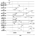
<動作>
本実施の形態における半導体デバイス駆動回路100の動作を説明する。図5に、半導体デバイス駆動回路100の動作シーケンスを示す。図5は、各接続点および各入力信号の電位の時間変化を表したものである。
<Operation>
An operation of the semiconductor device driving circuit 100 in the present embodiment will be described. FIG. 5 shows an operation sequence of the semiconductor device driving circuit 100. FIG. 5 shows the time change of the potential of each connection point and each input signal.
まず、初期動作について説明する。最初に、第1、2の電圧源11,12が始動する(動作101,102)。次に、正電位用コンデンサ17を初期充電するために、連続したパルス状のローサイド信号LINが入力回路1に入力される(動作103)。すると、ローサイドスイッチング素子6がオンになり(動作104)、第1の電圧源11によりコンデンサ17が充電される(動作105)。 First, the initial operation will be described. First, the first and second voltage sources 11 and 12 are started (operations 101 and 102). Next, in order to initially charge the positive potential capacitor 17, a continuous pulsed low-side signal LIN is input to the input circuit 1 (operation 103). Then, the low-side switching element 6 is turned on (operation 104), the capacitor 17 is charged by the first voltage source 11 (Operation 105).
また、スイッチ制御回路13にも連続したパルス状のスイッチ用信号LSAが入力され(動作106)、制御用スイッチング素子14がオンして(動作107)、第2の電圧源12により負電位用コンデンサ18が初期充電される(動作108)。 The pulse-shaped switching signal LSA which also continuously to the switch control circuit 13 is input (operation 106), the control switching element 14 is turned on (operation 107), a negative potential by the second voltage source 12 The capacitor 18 is initially charged (operation 108).
また、本実施の形態における半導体デバイス駆動装置は、半導体デバイス駆動回路100と、ハイサイドスイッチング素子5と、ローサイドスイッチング素子6と、負電位用コンデンサ18と、ブートストラップ回路20とをさらに備える。 The semiconductor device driving apparatus of this embodiment is further provided with a semiconductor device drive circuit 100, the high-side switching element 5, the low-side switching element 6, a negative potential capacitor 18, and a bootstrap circuit 20 .
本実施の形態における半導体デバイス駆動回路の動作を、図8のシーケンス図を用いて説明する。実施の形態1では、制御用スイッチング素子14は、ハイサイドスイッチング素子5のオン/オフに連動してオン/オフした。本実施の形態では、図8の動作221に示す様に、制御用スイッチング素子14は、ハイサイドスイッチング素子5のオンに連動してオンした後、一定時間後にオフする。その他の動作、即ち動作201〜220および動作222〜224は、実施の形態1の図5の動作101〜120および動作122〜124と同様なため、説明を省略する。 The operation of the semiconductor device drive circuit in this embodiment will be described with reference to the sequence diagram of FIG. In the first embodiment, the control switching element 14 is turned on / off in conjunction with the on / off of the high-side switching element 5. In the present embodiment, as shown in operation 221 of FIG. 8, the control switching element 14 is turned on in conjunction with the turning on of the high side switching element 5 and then turned off after a predetermined time. The other operations, that is, operations 201 to 220 and operations 222 to 224 are the same as the operations 101 to 120 and operations 122 to 124 of FIG.
<効果>
本実施の形態に係る半導体デバイス駆動回路100において、制御用スイッチング素子14がオンしてからオフするまでの時間を調整することが可能である。
<Effect>
In the semiconductor device drive circuit 100 according to the present embodiment, it is possible to adjust the time from when the control switching element 14 is turned on to when it is turned off.
<動作>
電圧クランプ回路16Aは、実施の形態1における電圧クランプ回路16と同様、負電位用コンデンサ18の両端の電圧が所定値を超えることを防止する回路である。本実施の形態における電圧クランプ回路16Aは、負電位用コンデンサ18の両端の電圧(即ち、接続点VSと接続点LVS間の電圧)が所定値を超えると、ハイレベルの信号DLVSを高圧逆レベルシフト回路51に対して出力する機能をさらに備える。電圧クランプ回路16Aに設定する電圧の所定値を、負電位用コンデンサ18が充電されたときの電圧とすることで、ハイレベルの信号DLVSは、負電位用コンデンサ18の充電完了を意味する信号となる。
<Operation>
Similar to the voltage clamp circuit 16 in the first embodiment, the voltage clamp circuit 16A is a circuit that prevents the voltage across the negative potential capacitor 18 from exceeding a predetermined value. Voltage clamp circuits 1 6 A in the present embodiment, the voltage across the negative potential capacitor 18 (i.e., the voltage between the connection point LVS and the connection point VS) when exceeds a predetermined value, the high level signal DLVS A function of outputting to the high-voltage reverse level shift circuit 51 is further provided. The predetermined value of the voltage to be set to the voltage clamping circuits 1 6 A, that a negative potential capacitor 18 and voltage when charged, the high level of the signal DLVS mean, fully charged negative potential capacitor 18 Signal.
高圧逆レベルシフト回路51は、接続点LVSと接続点VS間の電圧を基準とする信号のレベルを、接続点LGNDと正電位VCC間の電圧を基準とする信号のレベルに変換して出力する機能を備えた回路である。高圧逆レベルシフト回路51は、信号DLVSの基準電位を変換して、信号LSCとしてスイッチ制御回路13Bに出力する。 High-pressure reverse level shift circuit 51, the level of the signal relative to the voltage between the connection point VS and the connection point LVS, and converts the level of the signal relative to the voltage between the connection point LGND and Tadashiden position VCC Output This circuit has the function of The high-voltage reverse level shift circuit 51 converts the reference potential of the signal DLVS and outputs it as the signal LSC to the switch control circuit 13B.
本実施の形態におけるスイッチ制御回路13Bは、実施の形態1のスイッチ制御回路13と比較して、信号LSCがさらに入力される。入力回路1から入力される信号LSBがハイレベルの場合であって、かつ信号LSCがハイレベルとなった場合、スイッチ制御回路13Bは、ローレベルの信号を端子SOUTから出力する。つまり、負電位用コンデンサ18の両端の電圧が所定値に達したことを意味するハイレベルの信号LSCが入力されると、スイッチ制御回路13Bは、制御用スイッチング素子14をオフする。制御用スイッチング素子14がオフされることで、負電位用コンデンサ18の充電が停止する。その他の動作は実施の形態1と同じであるため、説明を省略する。 Compared with the switch control circuit 13 of the first embodiment, the switch control circuit 13B in the present embodiment further receives a signal LSC. The signal LSB inputted from the input circuit 1 in a case of a high level, and if the signal LSC is at a high level, the switch control circuitry 1 3 B outputs a low level signal from the terminal SOUT. That is, when the voltage across the negative potential capacitor 18 signal LSC high level which means that you have reached the predetermined value is input, the switch control circuitry 1 3 B turns off the control switching element 14. When the control switching element 14 is turned off, the charging of the negative potential capacitor 18 is stopped. Since other operations are the same as those in the first embodiment, description thereof is omitted.
負電位用コンデンサ18の充電が完了して、負電位用コンデンサ18の両端の電圧(接続点VSと接続点LVS間の電圧)が所定値を超えると(動作323)、電圧クランプ回路からハイレベルの信号DLVSが出力されるため(動作324)、スイッチ制御回路13Bに入力される信号LSCのレベルがローレベルからハイレベルへ切り替わる。これにより、スイッチ制御回路13B内の接続点LSPの電位がハイレベルからローレベルへと変化するため(動作325)、出力SOUTの電位がローレベルとなり、制御用スイッチング素子14がオフされる(動作326)。制御用スイッチング素子14がオフすることにより、負電位用コンデンサ18の充電が停止される。 When charging of the negative potential capacitor 18 is completed and the voltage across the negative potential capacitor 18 (voltage between the connection point VS and the connection point LVS) exceeds a predetermined value (operation 323), the voltage clamp circuit sets the high level. since the signal DLVS is output (operation 324), the level of the signal LSC that is input to the switch control circuits 1 3 B is switched from the low level to the high level. Thus, since the potential of the connection point LSP switch control circuits 1 3 in B changes from the high level to the low level (operation 325), the potential of the output SOUT goes low, the control switching element 14 is turned off (Operation 326). When the control switching element 14 is turned off, the charging of the negative potential capacitor 18 is stopped.
本実施の形態においては、ハイサイドドライバ3、ローサイドドライバ4およびスイッチ制御回路13の前段に低圧レベルシフト回路71を設ける。低圧レベルシフト回路71は、入出力間で信号の基準電位を変化させる機能を有する回路であり、図15にその一例を示す。低圧レベルシフト回路71の入力側の電源の正極、負極はそれぞれ入力信号の基準電位に接続される。また、出力側の電源の負極は、出力信号の基準電位に接続される。例えば、ローサイドドライバ4の前段に設けられる低圧レベルシフト回路71の場合、入力側の電源の正極、負極は、正電位VCCと基準電位GNDにそれぞれ接続され、出力側の電源の負極は基準電位LGNDに接続される。その他の構成は実施の形態1(図1)と同じであるため、説明を省略する。 In the present embodiment, a low voltage level shift circuit 71 is provided before the high side driver 3, the low side driver 4 and the switch control circuit 13. Low level shift circuit 71 is a circuit having a function of changing the reference potential of the signal between input and output, an example of which is shown in Figure 1 5. The positive and negative electrodes of the power supply on the input side of the low voltage level shift circuit 71 are connected to the reference potential of the input signal. The negative electrode of the power supply on the output side is connected to the reference potential of the output signal. For example, in the case of the low-voltage level shift circuit 71 provided in the preceding stage of the low-side driver 4, the positive and negative electrodes of the power supply on the input side are respectively connected to the positive potential VCC and the reference potential GND, and the negative electrode of the output power supply is the reference potential LGND. Connected to. Since other configurations are the same as those of the first embodiment (FIG. 1), description thereof is omitted.
ハイサイドドライバ3の負電位入力端子、即ち接続点LVSと、基準電位LGND(即ち実施の形態4における第2の電圧源12の負電位側)の間には、カソードが接続点LVSに接続された高耐圧のダイオード83と電流制限抵抗84とが直列に挿入される。また、接続点LVSと制御用スイッチング素子14のドレインとの間には、アノードが接続点LVSと接続されたダイオード82が挿入される。また、制御用スイッチング素子14のソースは基準電位GNDと接続される。その他の構成は、実施の形態4(図14)と同じであるため、説明を省略する。 A cathode is connected to the connection point LVS between the negative potential input terminal of the high side driver 3, that is, the connection point LVS and the reference potential LGND (that is, the negative potential side of the second voltage source 12 in the fourth embodiment). A high breakdown voltage diode 83 and a current limiting resistor 84 are inserted in series. A diode 82 having an anode connected to the connection point LVS is inserted between the connection point LVS and the drain of the control switching element 14. The source of the control switching element 14 is connected to the reference potential GND. Other configurations are the same as those of the fourth embodiment (FIG. 14), and thus description thereof is omitted.
<動作>
ハイサイドスイッチング素子5がオンの間は、高電圧源8により、負電位用コンデンサ18の充電とハイサイドドライバ3の負電位入力端子への負電位印加が行われる。
<Operation>
While the high side switching element 5 is on, the high voltage source 8 charges the negative potential capacitor 18 and applies a negative potential to the negative potential input terminal of the high side driver 3.
図18のシーケンス図を用いて、半導体デバイス駆動回路500の動作を詳しく説明する。まず、初期動作について説明する。最初に、第1の電圧源11が始動する(動作501)。次に、正電位用コンデンサ17を初期充電するために、連続したパルス状のローサイド信号LINが入力回路1に入力される(動作502)。すると、ローサイドスイッチング素子6がオンになり(動作503)、第1の電圧源11により正電位用コンデンサ17が充電される(動作504)。 The operation of the semiconductor device drive circuit 500 will be described in detail with reference to the sequence diagram of FIG. First, the initial operation will be described. First, the first voltage source 11 is started (operation 50 1) . Next, in order to initially charge the positive potential capacitor 17, a continuous pulsed low-side signal LIN is input to the input circuit 1 (operation 502). Then, the low-side switching element 6 is turned on (operation 503), a positive potential capacitor 17 is charged by the first voltage source 11 (Operation 504).
また、スイッチ制御回路13にも連続したパルス状のスイッチ用信号LSAが入力され(動作505)、制御用スイッチング素子14がオンするが(動作506)、負電位用コンデンサ18は充電されない(動作507)。 The pulse-shaped switching signal LSA which also continuously to the switch control circuit 13 is input (operation 505), but control the switching element 14 is turned on (operation 506), a negative potential capacitor 18 is not charged (Operation 507).
次に、通常動作について説明する。入力回路1にハイレベルのローサイド信号LINが入力されると(動作519)、ローサイドスイッチング素子6がオンになる(動作520)。このとき、ハイサイドスイッチング素子5および制御用スイッチング素子14はオフであり、ローサイドスイッチング素子6は、負電位用コンデンサ18、外部コンデンサ81、電流制限抵抗84およびダイオード83とともにループを形成する。よって、負電位用コンデンサ18が放電することによって(動作521)、外部コンデンサ81が充電される(動作522)。また、同時にローサイドドライバ4の負電位入力端子には、外部コンデンサ81の放電によって負電位が印加される。 Next, normal operation will be described. When a high-level low-side signal LIN is input to the input circuit 1 (operation 519), the low-side switching element 6 is turned on (operation 520). At this time, the high-side switching element 5 and the control switching element 14 are off, and the low-side switching element 6 forms a loop with the negative potential capacitor 18, the external capacitor 81, the current limiting resistor 84, and the diode 83. Therefore, when the negative potential capacitor 18 is discharged (operation 521), the external capacitor 81 is charged (operation 522). At the same time, a negative potential is applied to the negative potential input terminal of the low-side driver 4 by the discharge of the external capacitor 81.
ローサイドスイッチング素子6がオフすると、ローサイドドライバ4の負電位入力端子には、外部コンデンサ81の放電によって負電位が印加される(動作523)。 When the low-side switching element 6 is turned off, a negative potential is applied to the negative potential input terminal of the low-side driver 4 by the discharge of the external capacitor 81 (operation 523).
<効果>
本実施の形態における半導体デバイス駆動回路500は、ハイサイドドライバ3の負電位入力端子と第2の電圧源12の負電位側との間に接続されたダイオード83をさらに備え、ダイオード83のカソードはハイサイドドライバ3の負電位入力端子に接続されており、第2の電圧源12に代えて外部コンデンサ81が設けられ、ローサイドスイッチング素子6は、負電位用コンデンサ18、外部コンデンサ81およびダイオード83とともにループを形成することを特徴とする。
<Effect>
The semiconductor device drive circuit 500 in the present embodiment further includes a diode 83 connected between the negative potential input terminal of the high side driver 3 and the negative potential side of the second voltage source 12, and the cathode of the diode 83 is Connected to the negative potential input terminal of the high side driver 3, an external capacitor 81 is provided in place of the second voltage source 12, and the low side switching element 6 includes the negative potential capacitor 18, the external capacitor 81, and the diode 83. It is characterized by forming a loop.
Claims (2)
前記ダイオードのカソードは前記ハイサイドドライバの負電位入力端子に接続されており、
前記第2の電圧源に代えて外部コンデンサが設けられ、
前記ローサイドスイッチング素子は、前記負電位用コンデンサ、前記外部コンデンサおよび前記ダイオードとともにループを形成することを特徴とする、
請求項6に記載の半導体デバイス駆動回路。 A diode connected between the negative potential input terminal of the high side driver and the negative potential side of the second voltage source;
The cathode of the diode is connected to the negative potential input terminal of the high side driver,
An external capacitor is provided instead of the second voltage source,
The low-side switching element forms a loop together with the negative potential capacitor, the external capacitor and the diode,
The semiconductor device drive circuit according to claim 6.
前記ハイサイドスイッチング素子と、
前記ローサイドスイッチング素子と、
前記負電位用コンデンサと、
前記ブートストラップ回路と、
をさらに備える、
半導体デバイス駆動装置。 A semiconductor device driving circuit according to any one of claims 1 to 7;
The high-side switching element;
The low-side switching element;
The negative potential capacitor;
And the bootstrap circuit,
Further comprising
Semiconductor device drive device.
Priority Applications (3)
| Application Number | Priority Date | Filing Date | Title |
|---|---|---|---|
| JP2013061425A JP5991939B2 (en) | 2013-03-25 | 2013-03-25 | Semiconductor device driving circuit and semiconductor device driving apparatus |
| DE102014202643.1A DE102014202643B4 (en) | 2013-03-25 | 2014-02-13 | Semiconductor device drive circuit and semiconductor device drive unit |
| KR1020140031932A KR101603566B1 (en) | 2013-03-25 | 2014-03-19 | Semiconductor device drive circuit and semiconductor device drive unit |
Applications Claiming Priority (1)
| Application Number | Priority Date | Filing Date | Title |
|---|---|---|---|
| JP2013061425A JP5991939B2 (en) | 2013-03-25 | 2013-03-25 | Semiconductor device driving circuit and semiconductor device driving apparatus |
Publications (3)
| Publication Number | Publication Date |
|---|---|
| JP2014187825A JP2014187825A (en) | 2014-10-02 |
| JP2014187825A5 true JP2014187825A5 (en) | 2015-07-09 |
| JP5991939B2 JP5991939B2 (en) | 2016-09-14 |
Family
ID=51484862
Family Applications (1)
| Application Number | Title | Priority Date | Filing Date |
|---|---|---|---|
| JP2013061425A Active JP5991939B2 (en) | 2013-03-25 | 2013-03-25 | Semiconductor device driving circuit and semiconductor device driving apparatus |
Country Status (3)
| Country | Link |
|---|---|
| JP (1) | JP5991939B2 (en) |
| KR (1) | KR101603566B1 (en) |
| DE (1) | DE102014202643B4 (en) |
Families Citing this family (7)
| Publication number | Priority date | Publication date | Assignee | Title |
|---|---|---|---|---|
| JP6372607B2 (en) * | 2015-02-17 | 2018-08-15 | 株式会社村田製作所 | DC-DC converter |
| DE112017000186B4 (en) * | 2016-02-16 | 2022-05-05 | Fuji Electric Co., Ltd. | semiconductor device |
| WO2018102299A1 (en) * | 2016-12-01 | 2018-06-07 | Efficient Power Conversion Corporation | Bootstrap capacitor over-voltage management circuit for gan transistor based power converters |
| JP7032154B2 (en) * | 2018-01-31 | 2022-03-08 | ローム株式会社 | Switching circuits, semiconductor devices, DC / DC converters |
| JP7312561B2 (en) * | 2018-02-25 | 2023-07-21 | 新電元工業株式会社 | Power modules, switching power supplies and power control units |
| US11444337B2 (en) | 2019-03-12 | 2022-09-13 | Samsung Sdi Co., Ltd | Solid state switch driver circuit for a battery system |
| CN113746305B (en) * | 2021-08-30 | 2023-04-25 | 深圳数马电子技术有限公司 | Gate driving circuit and multiphase intelligent power module |
Family Cites Families (5)
| Publication number | Priority date | Publication date | Assignee | Title |
|---|---|---|---|---|
| JP2571963Y2 (en) * | 1991-11-21 | 1998-05-20 | 株式会社東芝 | Inverter device |
| JP4848714B2 (en) * | 2005-09-21 | 2011-12-28 | 富士電機株式会社 | Semiconductor power converter |
| JP5310425B2 (en) | 2009-09-15 | 2013-10-09 | 株式会社デンソー | Power converter |
| JP5640731B2 (en) * | 2010-12-24 | 2014-12-17 | サンケン電気株式会社 | Drive circuit and switching power supply device |
| JP2013062717A (en) * | 2011-09-14 | 2013-04-04 | Mitsubishi Electric Corp | Semiconductor device |
-
2013
- 2013-03-25 JP JP2013061425A patent/JP5991939B2/en active Active
-
2014
- 2014-02-13 DE DE102014202643.1A patent/DE102014202643B4/en active Active
- 2014-03-19 KR KR1020140031932A patent/KR101603566B1/en active IP Right Grant
Similar Documents
| Publication | Publication Date | Title |
|---|---|---|
| JP2014187825A5 (en) | ||
| JP5315026B2 (en) | Semiconductor device | |
| JP5991939B2 (en) | Semiconductor device driving circuit and semiconductor device driving apparatus | |
| JP2017529046A5 (en) | ||
| US20140078624A1 (en) | Semiconductor integrated circuit with esd protection circuit | |
| JP2006302971A (en) | Power supply clamp circuit and semiconductor device | |
| JP2009050118A (en) | Method of controlling gate driving circuit | |
| US9923557B2 (en) | Switching circuit and power conversion circuit | |
| JP2011139403A (en) | Power supply control circuit | |
| JP2007336694A (en) | Drive circuit for insulated-gate semiconductor device | |
| JP4747932B2 (en) | Relay drive circuit | |
| JP6138354B2 (en) | Load drive circuit and load short circuit detection circuit | |
| JP2016171676A (en) | Power supply circuit and control method therefor | |
| US9791882B2 (en) | Voltage source | |
| JP5481042B2 (en) | Overvoltage protection circuit and electronic device using the same | |
| JP2015100240A (en) | Protection device and transformation system | |
| TWI663408B (en) | Voltage detection circuit | |
| JP2015231117A (en) | Gate potential control circuit | |
| WO2018150789A1 (en) | Switch circuit | |
| TWI702797B (en) | Output circuit | |
| JP5405299B2 (en) | Circuit arrangement and method for controlling a power consuming device | |
| JP2016046993A (en) | Power supply apparatus and power supply method | |
| US20160026200A1 (en) | Power supply circuit | |
| JP2014150654A (en) | Gate Drive circuit | |
| JP2017537544A5 (en) |