JP2014187233A - Heat radiation sheet and heat radiation structure using the same - Google Patents
Heat radiation sheet and heat radiation structure using the same Download PDFInfo
- Publication number
- JP2014187233A JP2014187233A JP2013061413A JP2013061413A JP2014187233A JP 2014187233 A JP2014187233 A JP 2014187233A JP 2013061413 A JP2013061413 A JP 2013061413A JP 2013061413 A JP2013061413 A JP 2013061413A JP 2014187233 A JP2014187233 A JP 2014187233A
- Authority
- JP
- Japan
- Prior art keywords
- heat
- high thermal
- sheet
- resin sheet
- thermal conductive
- Prior art date
- Legal status (The legal status is an assumption and is not a legal conclusion. Google has not performed a legal analysis and makes no representation as to the accuracy of the status listed.)
- Pending
Links
Images

Classifications
-
- B—PERFORMING OPERATIONS; TRANSPORTING
- B32—LAYERED PRODUCTS
- B32B—LAYERED PRODUCTS, i.e. PRODUCTS BUILT-UP OF STRATA OF FLAT OR NON-FLAT, e.g. CELLULAR OR HONEYCOMB, FORM
- B32B9/00—Layered products comprising a layer of a particular substance not covered by groups B32B11/00 - B32B29/00
- B32B9/04—Layered products comprising a layer of a particular substance not covered by groups B32B11/00 - B32B29/00 comprising such particular substance as the main or only constituent of a layer, which is next to another layer of the same or of a different material
- B32B9/045—Layered products comprising a layer of a particular substance not covered by groups B32B11/00 - B32B29/00 comprising such particular substance as the main or only constituent of a layer, which is next to another layer of the same or of a different material of synthetic resin
-
- B—PERFORMING OPERATIONS; TRANSPORTING
- B32—LAYERED PRODUCTS
- B32B—LAYERED PRODUCTS, i.e. PRODUCTS BUILT-UP OF STRATA OF FLAT OR NON-FLAT, e.g. CELLULAR OR HONEYCOMB, FORM
- B32B7/00—Layered products characterised by the relation between layers; Layered products characterised by the relative orientation of features between layers, or by the relative values of a measurable parameter between layers, i.e. products comprising layers having different physical, chemical or physicochemical properties; Layered products characterised by the interconnection of layers
- B32B7/02—Physical, chemical or physicochemical properties
- B32B7/022—Mechanical properties
-
- B—PERFORMING OPERATIONS; TRANSPORTING
- B32—LAYERED PRODUCTS
- B32B—LAYERED PRODUCTS, i.e. PRODUCTS BUILT-UP OF STRATA OF FLAT OR NON-FLAT, e.g. CELLULAR OR HONEYCOMB, FORM
- B32B7/00—Layered products characterised by the relation between layers; Layered products characterised by the relative orientation of features between layers, or by the relative values of a measurable parameter between layers, i.e. products comprising layers having different physical, chemical or physicochemical properties; Layered products characterised by the interconnection of layers
- B32B7/02—Physical, chemical or physicochemical properties
- B32B7/027—Thermal properties
-
- B—PERFORMING OPERATIONS; TRANSPORTING
- B32—LAYERED PRODUCTS
- B32B—LAYERED PRODUCTS, i.e. PRODUCTS BUILT-UP OF STRATA OF FLAT OR NON-FLAT, e.g. CELLULAR OR HONEYCOMB, FORM
- B32B9/00—Layered products comprising a layer of a particular substance not covered by groups B32B11/00 - B32B29/00
- B32B9/04—Layered products comprising a layer of a particular substance not covered by groups B32B11/00 - B32B29/00 comprising such particular substance as the main or only constituent of a layer, which is next to another layer of the same or of a different material
-
- H—ELECTRICITY
- H01—ELECTRIC ELEMENTS
- H01L—SEMICONDUCTOR DEVICES NOT COVERED BY CLASS H10
- H01L23/00—Details of semiconductor or other solid state devices
- H01L23/34—Arrangements for cooling, heating, ventilating or temperature compensation ; Temperature sensing arrangements
- H01L23/36—Selection of materials, or shaping, to facilitate cooling or heating, e.g. heatsinks
- H01L23/373—Cooling facilitated by selection of materials for the device or materials for thermal expansion adaptation, e.g. carbon
- H01L23/3737—Organic materials with or without a thermoconductive filler
-
- H—ELECTRICITY
- H05—ELECTRIC TECHNIQUES NOT OTHERWISE PROVIDED FOR
- H05K—PRINTED CIRCUITS; CASINGS OR CONSTRUCTIONAL DETAILS OF ELECTRIC APPARATUS; MANUFACTURE OF ASSEMBLAGES OF ELECTRICAL COMPONENTS
- H05K1/00—Printed circuits
- H05K1/02—Details
- H05K1/0201—Thermal arrangements, e.g. for cooling, heating or preventing overheating
- H05K1/0203—Cooling of mounted components
- H05K1/0209—External configuration of printed circuit board adapted for heat dissipation, e.g. lay-out of conductors, coatings
-
- H—ELECTRICITY
- H05—ELECTRIC TECHNIQUES NOT OTHERWISE PROVIDED FOR
- H05K—PRINTED CIRCUITS; CASINGS OR CONSTRUCTIONAL DETAILS OF ELECTRIC APPARATUS; MANUFACTURE OF ASSEMBLAGES OF ELECTRICAL COMPONENTS
- H05K1/00—Printed circuits
- H05K1/18—Printed circuits structurally associated with non-printed electric components
- H05K1/181—Printed circuits structurally associated with non-printed electric components associated with surface mounted components
-
- H—ELECTRICITY
- H05—ELECTRIC TECHNIQUES NOT OTHERWISE PROVIDED FOR
- H05K—PRINTED CIRCUITS; CASINGS OR CONSTRUCTIONAL DETAILS OF ELECTRIC APPARATUS; MANUFACTURE OF ASSEMBLAGES OF ELECTRICAL COMPONENTS
- H05K7/00—Constructional details common to different types of electric apparatus
- H05K7/20—Modifications to facilitate cooling, ventilating, or heating
- H05K7/2039—Modifications to facilitate cooling, ventilating, or heating characterised by the heat transfer by conduction from the heat generating element to a dissipating body
- H05K7/20509—Multiple-component heat spreaders; Multi-component heat-conducting support plates; Multi-component non-closed heat-conducting structures
-
- B—PERFORMING OPERATIONS; TRANSPORTING
- B32—LAYERED PRODUCTS
- B32B—LAYERED PRODUCTS, i.e. PRODUCTS BUILT-UP OF STRATA OF FLAT OR NON-FLAT, e.g. CELLULAR OR HONEYCOMB, FORM
- B32B2307/00—Properties of the layers or laminate
- B32B2307/30—Properties of the layers or laminate having particular thermal properties
- B32B2307/302—Conductive
-
- B—PERFORMING OPERATIONS; TRANSPORTING
- B32—LAYERED PRODUCTS
- B32B—LAYERED PRODUCTS, i.e. PRODUCTS BUILT-UP OF STRATA OF FLAT OR NON-FLAT, e.g. CELLULAR OR HONEYCOMB, FORM
- B32B2307/00—Properties of the layers or laminate
- B32B2307/50—Properties of the layers or laminate having particular mechanical properties
-
- B—PERFORMING OPERATIONS; TRANSPORTING
- B32—LAYERED PRODUCTS
- B32B—LAYERED PRODUCTS, i.e. PRODUCTS BUILT-UP OF STRATA OF FLAT OR NON-FLAT, e.g. CELLULAR OR HONEYCOMB, FORM
- B32B2307/00—Properties of the layers or laminate
- B32B2307/70—Other properties
- B32B2307/732—Dimensional properties
-
- B—PERFORMING OPERATIONS; TRANSPORTING
- B32—LAYERED PRODUCTS
- B32B—LAYERED PRODUCTS, i.e. PRODUCTS BUILT-UP OF STRATA OF FLAT OR NON-FLAT, e.g. CELLULAR OR HONEYCOMB, FORM
- B32B2457/00—Electrical equipment
-
- B—PERFORMING OPERATIONS; TRANSPORTING
- B32—LAYERED PRODUCTS
- B32B—LAYERED PRODUCTS, i.e. PRODUCTS BUILT-UP OF STRATA OF FLAT OR NON-FLAT, e.g. CELLULAR OR HONEYCOMB, FORM
- B32B2457/00—Electrical equipment
- B32B2457/08—PCBs, i.e. printed circuit boards
-
- B—PERFORMING OPERATIONS; TRANSPORTING
- B32—LAYERED PRODUCTS
- B32B—LAYERED PRODUCTS, i.e. PRODUCTS BUILT-UP OF STRATA OF FLAT OR NON-FLAT, e.g. CELLULAR OR HONEYCOMB, FORM
- B32B2571/00—Protective equipment
-
- B—PERFORMING OPERATIONS; TRANSPORTING
- B32—LAYERED PRODUCTS
- B32B—LAYERED PRODUCTS, i.e. PRODUCTS BUILT-UP OF STRATA OF FLAT OR NON-FLAT, e.g. CELLULAR OR HONEYCOMB, FORM
- B32B27/00—Layered products comprising a layer of synthetic resin
- B32B27/30—Layered products comprising a layer of synthetic resin comprising vinyl (co)polymers; comprising acrylic (co)polymers
- B32B27/302—Layered products comprising a layer of synthetic resin comprising vinyl (co)polymers; comprising acrylic (co)polymers comprising aromatic vinyl (co)polymers, e.g. styrenic (co)polymers
-
- B—PERFORMING OPERATIONS; TRANSPORTING
- B32—LAYERED PRODUCTS
- B32B—LAYERED PRODUCTS, i.e. PRODUCTS BUILT-UP OF STRATA OF FLAT OR NON-FLAT, e.g. CELLULAR OR HONEYCOMB, FORM
- B32B3/00—Layered products comprising a layer with external or internal discontinuities or unevennesses, or a layer of non-planar form; Layered products having particular features of form
- B32B3/02—Layered products comprising a layer with external or internal discontinuities or unevennesses, or a layer of non-planar form; Layered products having particular features of form characterised by features of form at particular places, e.g. in edge regions
- B32B3/08—Layered products comprising a layer with external or internal discontinuities or unevennesses, or a layer of non-planar form; Layered products having particular features of form characterised by features of form at particular places, e.g. in edge regions characterised by added members at particular parts
-
- B—PERFORMING OPERATIONS; TRANSPORTING
- B32—LAYERED PRODUCTS
- B32B—LAYERED PRODUCTS, i.e. PRODUCTS BUILT-UP OF STRATA OF FLAT OR NON-FLAT, e.g. CELLULAR OR HONEYCOMB, FORM
- B32B7/00—Layered products characterised by the relation between layers; Layered products characterised by the relative orientation of features between layers, or by the relative values of a measurable parameter between layers, i.e. products comprising layers having different physical, chemical or physicochemical properties; Layered products characterised by the interconnection of layers
- B32B7/04—Interconnection of layers
- B32B7/12—Interconnection of layers using interposed adhesives or interposed materials with bonding properties
-
- B—PERFORMING OPERATIONS; TRANSPORTING
- B32—LAYERED PRODUCTS
- B32B—LAYERED PRODUCTS, i.e. PRODUCTS BUILT-UP OF STRATA OF FLAT OR NON-FLAT, e.g. CELLULAR OR HONEYCOMB, FORM
- B32B9/00—Layered products comprising a layer of a particular substance not covered by groups B32B11/00 - B32B29/00
- B32B9/005—Layered products comprising a layer of a particular substance not covered by groups B32B11/00 - B32B29/00 comprising one layer of ceramic material, e.g. porcelain, ceramic tile
- B32B9/007—Layered products comprising a layer of a particular substance not covered by groups B32B11/00 - B32B29/00 comprising one layer of ceramic material, e.g. porcelain, ceramic tile comprising carbon, e.g. graphite, composite carbon
-
- H—ELECTRICITY
- H01—ELECTRIC ELEMENTS
- H01L—SEMICONDUCTOR DEVICES NOT COVERED BY CLASS H10
- H01L2924/00—Indexing scheme for arrangements or methods for connecting or disconnecting semiconductor or solid-state bodies as covered by H01L24/00
- H01L2924/0001—Technical content checked by a classifier
- H01L2924/0002—Not covered by any one of groups H01L24/00, H01L24/00 and H01L2224/00
-
- H—ELECTRICITY
- H05—ELECTRIC TECHNIQUES NOT OTHERWISE PROVIDED FOR
- H05K—PRINTED CIRCUITS; CASINGS OR CONSTRUCTIONAL DETAILS OF ELECTRIC APPARATUS; MANUFACTURE OF ASSEMBLAGES OF ELECTRICAL COMPONENTS
- H05K2203/00—Indexing scheme relating to apparatus or processes for manufacturing printed circuits covered by H05K3/00
- H05K2203/13—Moulding and encapsulation; Deposition techniques; Protective layers
- H05K2203/1305—Moulding and encapsulation
- H05K2203/1311—Foil encapsulation, e.g. of mounted components
-
- H—ELECTRICITY
- H05—ELECTRIC TECHNIQUES NOT OTHERWISE PROVIDED FOR
- H05K—PRINTED CIRCUITS; CASINGS OR CONSTRUCTIONAL DETAILS OF ELECTRIC APPARATUS; MANUFACTURE OF ASSEMBLAGES OF ELECTRICAL COMPONENTS
- H05K2203/00—Indexing scheme relating to apparatus or processes for manufacturing printed circuits covered by H05K3/00
- H05K2203/13—Moulding and encapsulation; Deposition techniques; Protective layers
- H05K2203/1305—Moulding and encapsulation
- H05K2203/1322—Encapsulation comprising more than one layer
Abstract
Description
本発明は、各種電子機器に用いられる放熱シートおよびこれを用いた放熱構造に関するものである。 The present invention relates to a heat dissipation sheet used in various electronic devices and a heat dissipation structure using the same.
近年電子機器の各種機能や処理能力等が急速に向上し、それに伴い半導体素子をはじめとする電子部品からの発熱量は増加する傾向にある。このため半導体素子等の動作特性や信頼性等を保つために、樹脂に熱伝導性フィラーを混ぜて硬化した熱伝導シートを発熱部品に当接させ、放熱あるいは伝熱を行うことが行われている。 In recent years, various functions and processing capabilities of electronic devices have rapidly improved, and accordingly, the amount of heat generated from electronic components such as semiconductor elements tends to increase. For this reason, in order to maintain the operational characteristics and reliability of semiconductor elements, etc., a heat conductive sheet mixed with a heat conductive filler and cured is brought into contact with a heat generating component to perform heat dissipation or heat transfer. Yes.
なお、この出願の発明に関連する先行技術文献情報としては、例えば、特許文献1が知られている。 As prior art document information related to the invention of this application, for example, Patent Document 1 is known.
上記従来の熱伝導シートでは、発熱部品と熱伝導シートとの間の熱抵抗、熱伝導シートそのものの熱伝導率等により、十分に放熱、伝熱を行うことが難しかった。また接触状態による熱抵抗を下げるために、熱伝導シートを用いる代わりに、液状の樹脂に熱伝導フィラーを混ぜ、これを発熱部品に塗布して硬化させるという方法もあるが、この場合リペアすることができないという課題があった。 In the conventional heat conductive sheet, it is difficult to sufficiently dissipate and transfer heat due to the thermal resistance between the heat generating component and the heat conductive sheet, the heat conductivity of the heat conductive sheet itself, and the like. In addition, in order to reduce the thermal resistance due to the contact state, instead of using a heat conductive sheet, there is also a method of mixing a heat conductive filler in a liquid resin and applying it to a heat-generating component and curing it. There was a problem that it was not possible.
本発明はこの課題に対して、接触状態による熱抵抗を下げるとともに熱伝導性を向上させ、さらにリペア性にも優れた放熱シートを提供することを目的とする。 An object of the present invention is to provide a heat-dissipating sheet that lowers the thermal resistance due to the contact state, improves thermal conductivity, and is excellent in repairability.
本発明は上記課題を解決するために、常温で塑性変形可能な高熱伝導樹脂シートに、この高熱伝導樹脂シートよりも熱伝導率の高い高熱伝導フィルムを貼り合せたものである。 In order to solve the above-mentioned problems, the present invention is such that a high thermal conductive film having a higher thermal conductivity than this high thermal conductive resin sheet is bonded to a high thermal conductive resin sheet that can be plastically deformed at room temperature.
上記構成によりこの放熱シートを、発熱部品を含む電子部品を実装したプリント基板上に加圧して貼り合せたときに、高熱伝導樹脂シートを発熱部品の上面および側面に接触させることができ、熱抵抗を下げることができる。さらに高熱伝導樹脂シートには、高熱伝導樹脂シートよりも熱伝導率の高い高熱伝導フィルムを貼り合せているため、発熱部品から発生した熱は速やかに高熱伝導樹脂シートから高熱伝導フィルムに伝達され、放熱あるいは伝熱されるため、発熱部品の温度を抑えることができる。さらに高熱伝導樹脂シートを加熱硬化させること無くプリント基板に貼り合せすることができるため、リペア性に優れたものとなる。 With this configuration, when this heat-dissipating sheet is pressed and bonded onto a printed circuit board on which electronic components including heat-generating components are mounted, the high thermal conductive resin sheet can be brought into contact with the top and side surfaces of the heat-generating components, and the thermal resistance Can be lowered. Furthermore, since the high thermal conductive resin sheet is bonded with a high thermal conductive film having a higher thermal conductivity than the high thermal conductive resin sheet, the heat generated from the heat generating component is quickly transferred from the high thermal conductive resin sheet to the high thermal conductive film, Since the heat is radiated or transferred, the temperature of the heat generating component can be suppressed. Further, since the high thermal conductive resin sheet can be bonded to the printed circuit board without being cured by heating, the repair property is excellent.
以下、本発明の一実施の形態における放熱シートについて、図面を参照しながら説明する。 Hereinafter, a heat dissipation sheet according to an embodiment of the present invention will be described with reference to the drawings.
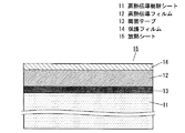
図1は本発明の一実施の形態における放熱シート15の断面図であり、厚さ1.3mmのスチレンポリマーからなる高熱伝導樹脂シート11に、高熱伝導フィルム12として厚さ25μmのグラファイトフィルムが、厚さ10μmの両面テープ13を介して貼り合されている。さらに高熱伝導フィルム12の上には厚さ10μmの保護フィルム14が貼り合されている。
FIG. 1 is a cross-sectional view of a
高熱伝導樹脂シート11は絶縁性および常温で塑性変形可能なものとなっている。ここで塑性変形可能とは、0.5MPa以下の圧力で形状が変形し、その圧力を除いても変形したままの形状を保持するものをいう。通常のスチレンポリマー等の樹脂シートでは、このような圧力に対して弾性変形する。これに対してこの材料に可塑剤を多く入れることにより、小さな圧力でも常温で塑性変形可能なものを得ることができる。
The high thermal
高熱伝導フィルム12は、熱分解グラファイトフィルムを用いることにより、面方向に1600W/m・Kの熱伝導率を有している。高熱伝導樹脂シート11は、2W/m・Kの熱伝導率を有している。高熱伝導樹脂シート11の熱伝導率は高い方が効率的に熱を運ぶことができるため、1W/m・K以上の熱伝導率を有していることが望ましい。しかしながら樹脂での熱伝導率はあまり大きなものが得られない。そこで本実施の形態のように高熱伝導樹脂シート11の上に、この高熱伝導樹脂シート11よりも遥かに大きな熱伝導率を有する高熱伝導フィルム12を貼り合せることにより、高熱伝導樹脂シート11に伝わった熱を速やかに高熱伝導フィルム12が面方向に拡散させることができ、本実施形態のように2W/m・K程度の熱伝導率であっても、十分に放熱あるいは伝熱を行うことができる。そのため、高熱伝導フィルム12の熱伝導率は、高熱伝導樹脂シート11の熱伝導率の100倍以上とすることが望ましい。
The high thermal
また高熱伝導樹脂シート11の厚さは、0.5〜2mmとすることが望ましい。このようにすることにより、IC等の発熱部品と十分に接するようにできるため、効率の良い放熱シートを得ることができる。
The thickness of the high thermal
さらに図1のように、高熱伝導フィルム12の上に絶縁性を有する保護フィルム14を貼り合せておくことがより望ましい。このようにすることにより放熱シートの表面の絶縁性を確保するとともに、外力からの損傷を防ぐことができる。なおこの保護フィルム14は、両面に粘着性を有する両面テープであっても良い。このようにすることにより、放熱シートを筐体あるいはヒートシンクに接続することができ、より効率的に放熱あるいは伝熱を行うことができる。
Further, as shown in FIG. 1, it is more desirable to bond a
次に本発明の一実施の形態における放熱構造について説明する。 Next, the heat dissipation structure in one embodiment of the present invention will be described.
図2は、本発明の一実施の形態における放熱シート15をプリント基板16に貼り合せた状態を示す断面図である。
FIG. 2 is a cross-sectional view showing a state in which the
プリント基板16上にはIC等の発熱部品17およびその他の電子部品が実装されている。この発熱部品17の高さは1mmとなっている。放熱シート15は、厚さ1.3mmの高熱伝導樹脂シート11に高熱伝導フィルム12を貼り合せたものであり、高熱伝導樹脂シート11側をプリント基板16の発熱部品17を実装した面に押し付けることにより、高熱伝導樹脂シート11を塑性変形させプリント基板16に貼り合せている。ここで高熱伝導樹脂シート11は、発熱部品17の上面全体、側面およびプリント基板16の発熱部品17を実装している側の面に密着させている。
A
ここで高熱伝導樹脂シート11は、発熱部品17の側面には、少なくともその面積の半分以上は接するようにしている。弾性を有する樹脂を発熱部品に押し付けた場合、上面には接するようにできるが、側面についてはスプリングバックによりほとんど接していない状態となる。本実施の形態では高熱伝導樹脂シート11を塑性変形させることができるものを用いているため、側面についても十分に密着させることができる。またプリント基板16への貼り合せ前の高熱伝導樹脂シート11の厚さを、発熱部品17の高さよりも大きくしているため、高熱伝導樹脂シート11をプリント基板16の実装面に接するようにすることができる。
Here, the high thermal
以上のように構成することにより、発熱部品17で発生した熱の多くはその上面から高熱伝導樹脂シート11を通じて高熱伝導フィルム12に伝熱されるとともに、発熱部品17の側面側からも高熱伝導樹脂シート11に伝わり、一部はプリント基板16の方にも逃がすことができる。そのため従来の熱伝導シートに比べてはるかに効率よく放熱あるいは伝熱を行うことができる。
With the above configuration, most of the heat generated in the
また発熱部品17に当接された部分の、塑性変形された高熱伝導樹脂シート11の厚さ(図2のT1)を、0.4mmとしている。このようにT1を薄くすることにより発熱部品17から高熱伝導フィルム12に熱を速やかに伝えることができるため、T1の大きさを0.5mm以下とすることが望ましい。
In addition, the thickness (T1 in FIG. 2) of the plastically deformed high thermal
なお、プリント基板16に放熱シート15を貼り合せる方法としては、ローラによる加圧あるいは、弾性体で放熱シート15側からプレスするという方法を用いることができる。この場合、高熱伝導フィルム12の上にさらに保護フィルム14を設けておくことが望ましく、保護フィルム14には、高熱伝導フィルム12よりも引っ張り強度が強いものを用いることが望ましい。
In addition, as a method of bonding the
本発明に係る放熱シートおよびこれを用いた放熱構造は、発熱部品で発生した熱を効率よく放熱あるいは伝熱することができ、さらにリペア性にも優れたものを得ることができ、産業上有用である。 The heat radiating sheet according to the present invention and the heat radiating structure using the heat radiating sheet can efficiently radiate or transfer the heat generated in the heat-generating component, and can obtain a product having excellent repairability, which is industrially useful. It is.
11 高熱伝導樹脂シート
12 高熱伝導フィルム
13 両面テープ
14 保護フィルム
15 放熱シート
16 プリント基板
17 発熱部品
DESCRIPTION OF
Claims (8)
Priority Applications (4)
| Application Number | Priority Date | Filing Date | Title |
|---|---|---|---|
| JP2013061413A JP2014187233A (en) | 2013-03-25 | 2013-03-25 | Heat radiation sheet and heat radiation structure using the same |
| US14/778,583 US20160159037A1 (en) | 2013-03-25 | 2014-03-04 | Heat dissipating sheet and heat dissipating structural body using same |
| CN201480017887.3A CN105073404B (en) | 2013-03-25 | 2014-03-04 | Fin and the heat-radiating structure for having used the fin |
| PCT/JP2014/001164 WO2014155977A1 (en) | 2013-03-25 | 2014-03-04 | Heat dissipating sheet and heat dissipating structural body using same |
Applications Claiming Priority (1)
| Application Number | Priority Date | Filing Date | Title |
|---|---|---|---|
| JP2013061413A JP2014187233A (en) | 2013-03-25 | 2013-03-25 | Heat radiation sheet and heat radiation structure using the same |
Publications (1)
| Publication Number | Publication Date |
|---|---|
| JP2014187233A true JP2014187233A (en) | 2014-10-02 |
Family
ID=51622998
Family Applications (1)
| Application Number | Title | Priority Date | Filing Date |
|---|---|---|---|
| JP2013061413A Pending JP2014187233A (en) | 2013-03-25 | 2013-03-25 | Heat radiation sheet and heat radiation structure using the same |
Country Status (4)
| Country | Link |
|---|---|
| US (1) | US20160159037A1 (en) |
| JP (1) | JP2014187233A (en) |
| CN (1) | CN105073404B (en) |
| WO (1) | WO2014155977A1 (en) |
Cited By (4)
| Publication number | Priority date | Publication date | Assignee | Title |
|---|---|---|---|---|
| JP2017118025A (en) * | 2015-12-25 | 2017-06-29 | 昭和電工株式会社 | Electromagnetic shielding heat dissipation sheet and heat spreader |
| WO2018139364A1 (en) * | 2017-01-30 | 2018-08-02 | 積水ポリマテック株式会社 | Heat dissipation sheet |
| US10879145B2 (en) | 2016-10-14 | 2020-12-29 | Omron Corporation | Electronic device and method of manufacture therefor |
| KR20210002889A (en) * | 2019-07-01 | 2021-01-11 | 삼성전기주식회사 | Semiconductor package |
Families Citing this family (3)
| Publication number | Priority date | Publication date | Assignee | Title |
|---|---|---|---|---|
| JP7465816B2 (en) * | 2018-12-20 | 2024-04-11 | リンテック株式会社 | Method for manufacturing double-sided tape for protecting terminals and semiconductor device with electromagnetic wave shielding film |
| JP7379854B2 (en) * | 2019-04-19 | 2023-11-15 | 住友電気工業株式会社 | optical transceiver |
| CN111038019B (en) * | 2019-11-11 | 2022-06-14 | 中国商用飞机有限责任公司 | Composite material, aircraft component and anti-icing and deicing method |
Citations (8)
| Publication number | Priority date | Publication date | Assignee | Title |
|---|---|---|---|---|
| JPS62261199A (en) * | 1986-05-08 | 1987-11-13 | 富士通株式会社 | Heat radiation structure of printed wiring board on ehich electronic parts are mounted |
| JP2001291807A (en) * | 2000-04-10 | 2001-10-19 | Three M Innovative Properties Co | Thermo-conductive sheet |
| JP2003158393A (en) * | 2001-11-21 | 2003-05-30 | Shin Etsu Chem Co Ltd | Heat dissipation structure |
| JP2008091558A (en) * | 2006-09-29 | 2008-04-17 | Toshiba Corp | Heat dissipator |
| JP2008272976A (en) * | 2007-04-26 | 2008-11-13 | Kaneka Corp | Composite graphite film |
| JP2010171350A (en) * | 2009-01-26 | 2010-08-05 | Inoac Corp | Heat dissipation structure |
| JP2011187899A (en) * | 2010-03-11 | 2011-09-22 | Kaneka Corp | Heat dissipation structure |
| WO2012036788A2 (en) * | 2010-09-14 | 2012-03-22 | Laird Technologies, Inc. | Compliant multilayered thermally-conductive interface assemblies having emi shielding properties |
Family Cites Families (11)
| Publication number | Priority date | Publication date | Assignee | Title |
|---|---|---|---|---|
| US5198063A (en) * | 1991-06-03 | 1993-03-30 | Ucar Carbon Technology Corporation | Method and assembly for reinforcing flexible graphite and article |
| JPH1174667A (en) * | 1997-06-16 | 1999-03-16 | Nitto Denko Corp | Heat dissipation sheet |
| JP3068615B1 (en) * | 1999-08-02 | 2000-07-24 | 北川工業株式会社 | Heat conduction parts |
| US20030207128A1 (en) * | 2000-04-10 | 2003-11-06 | Tomoaki Uchiya | Thermally conductive sheet |
| JP3466135B2 (en) * | 2000-06-12 | 2003-11-10 | 北川工業株式会社 | Thermal conductive material |
| JP2003145041A (en) * | 2001-11-07 | 2003-05-20 | Three M Innovative Properties Co | Heat conductive sheet |
| JP2007294554A (en) * | 2006-04-24 | 2007-11-08 | Sumitomo Electric Ind Ltd | Convex structural member |
| US7928590B2 (en) * | 2006-08-15 | 2011-04-19 | Qimonda Ag | Integrated circuit package with a heat dissipation device |
| CN101796106B (en) * | 2007-09-05 | 2012-10-10 | 积水化学工业株式会社 | Insulating sheet and multilayer structure |
| JP5271879B2 (en) * | 2008-11-28 | 2013-08-21 | 富士高分子工業株式会社 | Thermal diffusion sheet and mounting method thereof |
| CN102602076B (en) * | 2012-03-01 | 2015-03-11 | 昆山市中迪新材料技术有限公司 | Heat conductive insulation sheet and structural adhesive |
-
2013
- 2013-03-25 JP JP2013061413A patent/JP2014187233A/en active Pending
-
2014
- 2014-03-04 WO PCT/JP2014/001164 patent/WO2014155977A1/en active Application Filing
- 2014-03-04 US US14/778,583 patent/US20160159037A1/en not_active Abandoned
- 2014-03-04 CN CN201480017887.3A patent/CN105073404B/en not_active Expired - Fee Related
Patent Citations (8)
| Publication number | Priority date | Publication date | Assignee | Title |
|---|---|---|---|---|
| JPS62261199A (en) * | 1986-05-08 | 1987-11-13 | 富士通株式会社 | Heat radiation structure of printed wiring board on ehich electronic parts are mounted |
| JP2001291807A (en) * | 2000-04-10 | 2001-10-19 | Three M Innovative Properties Co | Thermo-conductive sheet |
| JP2003158393A (en) * | 2001-11-21 | 2003-05-30 | Shin Etsu Chem Co Ltd | Heat dissipation structure |
| JP2008091558A (en) * | 2006-09-29 | 2008-04-17 | Toshiba Corp | Heat dissipator |
| JP2008272976A (en) * | 2007-04-26 | 2008-11-13 | Kaneka Corp | Composite graphite film |
| JP2010171350A (en) * | 2009-01-26 | 2010-08-05 | Inoac Corp | Heat dissipation structure |
| JP2011187899A (en) * | 2010-03-11 | 2011-09-22 | Kaneka Corp | Heat dissipation structure |
| WO2012036788A2 (en) * | 2010-09-14 | 2012-03-22 | Laird Technologies, Inc. | Compliant multilayered thermally-conductive interface assemblies having emi shielding properties |
Cited By (10)
| Publication number | Priority date | Publication date | Assignee | Title |
|---|---|---|---|---|
| JP2017118025A (en) * | 2015-12-25 | 2017-06-29 | 昭和電工株式会社 | Electromagnetic shielding heat dissipation sheet and heat spreader |
| US10879145B2 (en) | 2016-10-14 | 2020-12-29 | Omron Corporation | Electronic device and method of manufacture therefor |
| WO2018139364A1 (en) * | 2017-01-30 | 2018-08-02 | 積水ポリマテック株式会社 | Heat dissipation sheet |
| CN110301043A (en) * | 2017-01-30 | 2019-10-01 | 积水保力马科技株式会社 | Cooling fin |
| JPWO2018139364A1 (en) * | 2017-01-30 | 2019-12-26 | 積水ポリマテック株式会社 | Heat dissipation sheet |
| US11085712B2 (en) | 2017-01-30 | 2021-08-10 | Sekisui Polymatech Co., Ltd. | Heat-dissipating sheet |
| JP7152020B2 (en) | 2017-01-30 | 2022-10-12 | 積水ポリマテック株式会社 | Heat dissipation sheet |
| CN110301043B (en) * | 2017-01-30 | 2024-03-01 | 积水保力马科技株式会社 | Heat sink |
| KR20210002889A (en) * | 2019-07-01 | 2021-01-11 | 삼성전기주식회사 | Semiconductor package |
| KR102574409B1 (en) * | 2019-07-01 | 2023-09-04 | 삼성전기주식회사 | Semiconductor package |
Also Published As
| Publication number | Publication date |
|---|---|
| WO2014155977A1 (en) | 2014-10-02 |
| US20160159037A1 (en) | 2016-06-09 |
| CN105073404A (en) | 2015-11-18 |
| CN105073404B (en) | 2018-01-16 |
Similar Documents
| Publication | Publication Date | Title |
|---|---|---|
| JP2014187233A (en) | Heat radiation sheet and heat radiation structure using the same | |
| US10091868B2 (en) | Heat dissipating sheet and heat dissipating structure using same | |
| JP2006303240A (en) | Heat dissipating sheet, heat dissipating body, manufacturing method for the sheet, and heat transfer method | |
| JP4916764B2 (en) | Anisotropic heat conduction laminated heat dissipation member | |
| US10945331B2 (en) | Mobile display device | |
| JP6432918B1 (en) | Circuit board housing | |
| JP2008541490A (en) | Thermal lamination module | |
| JP2011222934A (en) | Thin heat dissipating device | |
| WO2013140741A1 (en) | Thermally conductive body and electronic device using same | |
| TW201204227A (en) | Heat dissipation apparatus | |
| JP2014063875A (en) | Printed circuit board | |
| JP3128948U (en) | Electric circuit board structure with heat dissipation layer | |
| CN208094874U (en) | Flexible circuit board structure with heat conduction through hole | |
| JP2020061482A (en) | Heat dissipation structure | |
| JP5018195B2 (en) | Heat dissipation device | |
| JP2010135459A (en) | Semiconductor package and heat radiator | |
| JP2014135374A (en) | Heat transfer substrate | |
| JP6543803B2 (en) | Thermal conduction sheet | |
| JP2008262948A (en) | Electronic component unit | |
| JP2015053311A (en) | Cooling system | |
| KR20140075255A (en) | Thermal diffusion sheet and the manufacturing method thereof | |
| KR20140075254A (en) | Thermal diffusion sheet and the manufacturing method thereof | |
| KR102071921B1 (en) | Heat spreading frame with high heat dissipating function | |
| JP6168360B2 (en) | Circuit structure and method for manufacturing circuit structure | |
| JP2014170835A (en) | Heat radiation structure of heating component and audio device using the same |
Legal Events
| Date | Code | Title | Description |
|---|---|---|---|
| A711 | Notification of change in applicant |
Free format text: JAPANESE INTERMEDIATE CODE: A711 Effective date: 20141006 |
|
| A621 | Written request for application examination |
Free format text: JAPANESE INTERMEDIATE CODE: A621 Effective date: 20151126 |
|
| RD01 | Notification of change of attorney |
Free format text: JAPANESE INTERMEDIATE CODE: A7421 Effective date: 20160518 |
|
| A131 | Notification of reasons for refusal |
Free format text: JAPANESE INTERMEDIATE CODE: A131 Effective date: 20160906 |
|
| A521 | Request for written amendment filed |
Free format text: JAPANESE INTERMEDIATE CODE: A523 Effective date: 20161027 |
|
| A131 | Notification of reasons for refusal |
Free format text: JAPANESE INTERMEDIATE CODE: A131 Effective date: 20170131 |
|
| A02 | Decision of refusal |
Free format text: JAPANESE INTERMEDIATE CODE: A02 Effective date: 20170725 |