JP2014143831A - Power conversion device - Google Patents
Power conversion device Download PDFInfo
- Publication number
- JP2014143831A JP2014143831A JP2013010701A JP2013010701A JP2014143831A JP 2014143831 A JP2014143831 A JP 2014143831A JP 2013010701 A JP2013010701 A JP 2013010701A JP 2013010701 A JP2013010701 A JP 2013010701A JP 2014143831 A JP2014143831 A JP 2014143831A
- Authority
- JP
- Japan
- Prior art keywords
- switching
- pulses
- pulse
- voltage
- phase
- Prior art date
- Legal status (The legal status is an assumption and is not a legal conclusion. Google has not performed a legal analysis and makes no representation as to the accuracy of the status listed.)
- Granted
Links
- 238000006243 chemical reaction Methods 0.000 title claims description 13
- 230000007704 transition Effects 0.000 claims abstract description 21
- 230000008859 change Effects 0.000 claims description 26
- 230000007274 generation of a signal involved in cell-cell signaling Effects 0.000 claims description 8
- 230000007935 neutral effect Effects 0.000 claims description 3
- 238000010586 diagram Methods 0.000 description 17
- 230000000052 comparative effect Effects 0.000 description 13
- 238000000034 method Methods 0.000 description 11
- 238000007796 conventional method Methods 0.000 description 6
- 230000008030 elimination Effects 0.000 description 6
- 238000003379 elimination reaction Methods 0.000 description 6
- 230000010349 pulsation Effects 0.000 description 6
- 230000001133 acceleration Effects 0.000 description 4
- 230000007423 decrease Effects 0.000 description 4
- 239000003990 capacitor Substances 0.000 description 2
- 238000012217 deletion Methods 0.000 description 2
- 230000037430 deletion Effects 0.000 description 2
- 230000014509 gene expression Effects 0.000 description 2
- 230000009467 reduction Effects 0.000 description 2
- 230000001360 synchronised effect Effects 0.000 description 2
- 230000003247 decreasing effect Effects 0.000 description 1
- 230000000694 effects Effects 0.000 description 1
- 230000008569 process Effects 0.000 description 1
- 230000004044 response Effects 0.000 description 1
- 230000002441 reversible effect Effects 0.000 description 1
- 230000001052 transient effect Effects 0.000 description 1
Images


Abstract
Description
この発明は、低次高調波消去PWM制御方式の電力変換装置に関するものである。 The present invention relates to a power converter using a low-order harmonic elimination PWM control method.
PWM制御方式としては一般的に三角波比較PWMが用いられるが、出力電圧の高調波を低減するためにはPWMキャリアの周波数を大きくする必要がある。しかし、大容量のインバータでは、スイッチング素子のスイッチング速度が遅いため、PWMキャリアの周波数を大きくすることができない。その結果、出力電圧に低次の高調波が残存する問題がある。そこで、少ないスイッチング回数を有効利用し、特定の低次の高調波を低減するタイミングでスイッチングを行う、低次高調波消去PWMがある(例えば、特許文献1、非特許文献1参照)。
A triangular wave comparison PWM is generally used as the PWM control method, but it is necessary to increase the frequency of the PWM carrier in order to reduce harmonics of the output voltage. However, in a large-capacity inverter, since the switching speed of the switching element is slow, the frequency of the PWM carrier cannot be increased. As a result, there is a problem that low-order harmonics remain in the output voltage. Therefore, there is a low-order harmonic elimination PWM that makes effective use of a small number of times of switching and performs switching at a timing at which a specific low-order harmonic is reduced (see, for example,
また、PWMパルスのパルス数を切り替える従来の方法では、以下のものがある。
パルスモード指令発生手段は、インバータ出力電圧の半周期あたりのパルス数を設定する。切り替え位相角発生手段は、5パルスモードと3パルスモード相互間の切り替え時のインバータ電流の過渡変動を最も小さくできる切り替え位相角を求めて出力する。パルスモード相別切り替え指令発生手段は、位相角指令値が切り替え位相角の範囲内である際に、各相ごとにパルスモード指令発生手段が設定するパルス数を指定する。このパルス数に応じて、各相の切り替え手段は、5パルスモードPWM信号発生手段または3パルスモードPWM信号発生手段から出力される各相のPWM信号に基づいてゲート信号を生成して出力する(例えば、特許文献2参照)。
Further, conventional methods for switching the number of PWM pulses include the following.
The pulse mode command generation means sets the number of pulses per half cycle of the inverter output voltage. The switching phase angle generating means obtains and outputs a switching phase angle that can minimize the transient fluctuation of the inverter current when switching between the 5-pulse mode and the 3-pulse mode. The pulse mode phase change command generation means specifies the number of pulses set by the pulse mode command generation means for each phase when the phase angle command value is within the range of the switch phase angle. Depending on the number of pulses, the switching means for each phase generates and outputs a gate signal based on the PWM signal for each phase output from the 5-pulse mode PWM signal generating means or the 3-pulse mode PWM signal generating means ( For example, see Patent Document 2).
上記のような低次高調波消去PWM制御は、互いに高調波を相殺する位相でパルスを出力するため、高調波損失や騒音の低減に非常に効果的である。しかしながら、運転周波数に応じてパルス数を切替える際に発生する電流変動については考慮されていない。
また、上記特許文献2で示したパルス数を切り替える従来の方法では、同期PWM方式で、各相の電圧面積(変調率)をそれぞれ一定に保てる位相で各相別に切替えることにより切替時の電流変動やトルク脈動を抑制する方法が開示されている。しかしながら、同期PWM方式自体が低次高調波が大きい。また、切り替えのパルス数条件は限られており、かつ、各相所定の位相で順次切り替えるため、切替位相によっては線間電圧が大きく変動し、電流変動やトルク脈動となるという問題点があった。
Since the low-order harmonic elimination PWM control as described above outputs pulses at a phase that cancels out the harmonics, it is very effective in reducing harmonic loss and noise. However, no consideration is given to current fluctuations that occur when the number of pulses is switched according to the operating frequency.
In the conventional method of switching the number of pulses shown in
この発明は、上記のような問題点を解決するためになされたもので、低次高調波を低減し、かつPWM制御によるパルス数切り替え時の電流変動を抑制できる電力変換装置を提供することを目的とする。 The present invention has been made to solve the above-described problems, and provides a power converter that can reduce low-order harmonics and suppress current fluctuation when switching the number of pulses by PWM control. Objective.
この発明による電力変換装置は、スイッチング素子を有して直流電圧源の電圧を任意の大きさおよび周波数の出力電圧に変換するインバータと、上記スイッチング素子をPWM制御する制御部とを備える。上記制御部は、上記出力電圧と上記直流電圧源の電圧とに基づいて変調率を演算する変調率演算手段と、上記スイッチング素子のPWM制御における半周期あたりのパルス数を上記インバータに設定される出力周波数に基づいて決定するパルス数決定手段と、上記出力電圧の低次高調波を低減し、かつ上記スイッチング素子の特性により決まる最小パルス幅を確保したスイッチングパターンを、パルス数別に変調率の大きさに応じて記憶する記憶手段と、上記変調率演算手段からの変調率と、上記パルス数決定手段からのパルス数とに基づいて上記記憶手段からのスイッチングパターンを用い、上記スイッチング素子を駆動するゲート信号を生成するゲート信号生成部と、上記パルス数決定手段からのパルス数が変化したとき、上記ゲート信号生成部が用いる上記スイッチングパターンを、変化後のパルス数に基づくスイッチングパターンに切り替える際に、上記出力電圧の変動を抑制する切替移行期間を設けるパルス数切替手段とを備えるものである。 A power conversion device according to the present invention includes an inverter that has a switching element and converts a voltage of a DC voltage source into an output voltage having an arbitrary magnitude and frequency, and a control unit that performs PWM control on the switching element. The control unit sets a modulation rate calculating means for calculating a modulation rate based on the output voltage and the voltage of the DC voltage source, and the number of pulses per half cycle in PWM control of the switching element is set in the inverter. A pulse number determining means that determines based on the output frequency, and a switching pattern that reduces the low-order harmonics of the output voltage and secures a minimum pulse width determined by the characteristics of the switching element, has a large modulation rate for each pulse number. The switching element is driven using the switching pattern from the storage means based on the storage means for storing in accordance with the modulation rate from the modulation rate calculation means and the pulse number from the pulse number determination means. When the number of pulses from the gate signal generation unit that generates the gate signal and the pulse number determination means changes, the gate signal The switching pattern generation unit is used, when switching the switching pattern based on the number of pulses after the change, in which and a pulse number switching means for providing a suppressing switching transition period of variation of the output voltage.
この発明による電力変換装置は上記のように構成されているため、低次高調波を低減し、かつPWM制御によるパルス数切り替え時に出力電圧および電流変動を抑制できる。また、パルス数切り替えを伴うモータ制御に適用した場合、トルク脈動の少ないモータ制御を実現できる。 Since the power converter according to the present invention is configured as described above, it is possible to reduce low-order harmonics and suppress output voltage and current fluctuations when switching the number of pulses by PWM control. In addition, when applied to motor control with pulse number switching, motor control with less torque pulsation can be realized.
実施の形態1.
以下、この発明の実施の形態1による電力変換装置を図に基づいて説明する。
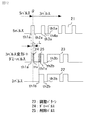
図1は、この発明の実施の形態1による電力変換装置の構成を示す図である。図1に示すように、電力変換装置2は、インバータ4とインバータ4を制御する制御部10とを備えて、直流電圧源1の直流電力を交流電力に変換してモータ3に供給する。
インバータ4は、直流電圧源1の電圧を分圧する2直列のコンデンサ5a、5bと、それぞれダイオードが逆並列接続されたIGBT等から成る複数のスイッチング素子6と、クランプダイオード7とを備えた中性点クランプ式の三相3レベルインバータにて構成され、スイッチング素子6のスイッチング動作によって直流電圧源1の電圧を任意の大きさ及び周波数の出力電圧に変換する。
Hereinafter, a power converter according to
1 is a diagram showing a configuration of a power conversion device according to
The
制御部10は、変調率mを演算する変調率演算手段としての変調率演算器11と、パルス数別に変調率mの大きさに応じて予め決定されたスイッチングパターンth1、th2、th3、・・を記憶する記憶手段としてのスイッチングパターンテーブル12とを備える。なお、パルス数とは、スイッチング素子6のPWM制御における半周期あたりのパルス数である。制御部10は、さらに、インバータ4に設定される出力周波数となる周波数指令値Fcからパルス数Pnumを決定するパルス数決定手段としてのパルス数決定部13と、パルス数決定部13からのパルス数Pnumが変化したときに、PWM制御のパルス数を切り替えるパルス数切替手段としてのパルス数切替部14と、インバータ4の各スイッチング素子6を駆動制御するゲート信号17を生成するゲート信号生成部としてのゲート発生器16とを備える。
The
次に動作を説明する。
変調率演算器11は、インバータ出力電圧の相電圧振幅Vpと直流電圧源1の電圧Vdcとから、次式で変調率mを演算する。
m=Vp/(Vdc/2) ・・・(1)
Next, the operation will be described.
The
m = Vp / (Vdc / 2) (1)
パルス数決定部13は、インバータ4の周波数指令値Fcに応じてPWM制御における半周期あたりのパルス数Pnumを決定する。例えば、周波数指令値Fcによるパルス数Pnumの判定基準は以下のようになる。
0≦Fc<F1 : Pnum=9
F1≦Fc<F2 : Pnum=7
F2≦Fc<F3 : Pnum=5
F3≦Fc : Pnum=3 ・・・(2)
The pulse
0 ≦ Fc <F1: Pnum = 9
F1 ≦ Fc <F2: Pnum = 7
F2 ≦ Fc <F3: Pnum = 5
F3 ≦ Fc: Pnum = 3 (2)
この場合、パルス数Pnumの判定基準となる周波数F1、F2、F3は定格周波数の1/4、1/2、3/4に設定する。 In this case, the frequencies F1, F2, and F3, which are determination criteria for the number of pulses Pnum, are set to 1/4, 1/2, and 3/4 of the rated frequency.
なお、判定基準となる周波数F1、F2、F3は定格周波数基準に限らず、キャリア周波数やPWM制御を行うマイコンの処理能力に応じて変える方法にしても良い。
また、周波数指令値Fcによるパルス数Pnumの切り替えは、図2に示すようにヒステリシス幅を有して切り替えても良い。
また、周波数指令値Fcにより相電圧振幅Vpの範囲が異なる場合もあり、周波数指令値Fcと相電圧振幅Vpとの組み合わせによってパルス数Pnumを決定しても良い。
Note that the frequencies F1, F2, and F3 serving as determination criteria are not limited to the rated frequency reference, and may be changed in accordance with the carrier frequency and the processing capability of the microcomputer that performs PWM control.
Further, switching of the pulse number Pnum by the frequency command value Fc may be performed with a hysteresis width as shown in FIG.
Further, the range of the phase voltage amplitude Vp may differ depending on the frequency command value Fc, and the pulse number Pnum may be determined by a combination of the frequency command value Fc and the phase voltage amplitude Vp.
スイッチングパターンテーブル12では、パルス数Pnum別に、変調率mの大きさ毎に出力電圧の低次高調波を低減できるスイッチングパターンth1、th2、・・・thnを記憶している。ここでは、変調率mを0.01刻みとしてスイッチングパターンを記憶し、その間は線形補完して用いるものとする。
そして、スイッチングパターンテーブル12は、パルス数決定部13からのパルス数Pnumと、変調率演算器11からの変調率mとに基づいて、スイッチングパターンth1、th2、・・・thnを導出する。
The switching pattern table 12 stores switching patterns th1, th2,... Thn that can reduce lower harmonics of the output voltage for each magnitude of the modulation factor m for each number of pulses Pnum. Here, it is assumed that the switching pattern is stored with the modulation factor m being incremented by 0.01 and linear interpolation is used during that time.
The switching pattern table 12 derives the switching patterns th1, th2,... Thn based on the pulse number Pnum from the pulse
例えば、パルス数Pnumが3の場合、インバータ4の各3レベルレグが、基本波の1/4周期に3回、スイッチング素子6によるスイッチングを行うが、ゲート発生器16では、この時のスイッチングパターンth1、th2、th3に基づき、出力電圧の位相thに応じてゲート信号17を生成して出力する。そして、インバータ4の各相は、図3に示すように、半周期に3パルスの相電圧を出力する。三相では各相が2π/3ずつシフトした波形になる。
なお、図3では、基本波の半周期に単一極性のパルスを複数出力するユニポーラ変調のパルスパターンを図示した。大容量インバータの場合、低次高調波消去PWMのスイッチングパターンに高電圧の制御がしやすいユニポーラ変調のパルスパターンを用いるのが一般的であるが、ダイポーラ変調のパルスパターンも適用できる。
For example, when the number of pulses Pnum is 3, each of the three level legs of the
FIG. 3 shows a pulse pattern of unipolar modulation that outputs a plurality of pulses having a single polarity in a half cycle of the fundamental wave. In the case of a large-capacity inverter, it is common to use a unipolar modulation pulse pattern that can easily control a high voltage as the switching pattern of the low-order harmonic elimination PWM, but a dipolar modulation pulse pattern can also be applied.
また、周波数指令値Fcによって決まるパルス数Pnumが変化すると、スイッチングパターンテーブル12から導出されるスイッチングパターンth1、th2、・・・thnも切り替わるものであるが、パルス数切替部14では、切替移行期間を設けてスイッチングパターンを切り替えるタイミングを調整する。これは、スイッチングパターンの変化により発生する電圧変動によりモータ電流が大きく変動するのを抑制するためのもので、パルス数切替部14からの切替指令15により、変化後のパルス数Pnumに基づくスイッチングパターンに、調整後のタイミングで切り替わる。
Further, when the number of pulses Pnum determined by the frequency command value Fc changes, the switching patterns th1, th2,... Thn derived from the switching pattern table 12 are also switched. To adjust the timing of switching the switching pattern. This is for suppressing the motor current from largely fluctuating due to voltage fluctuations caused by the change of the switching pattern. The switching pattern based on the changed pulse number Pnum by the switching
次に、スイッチングパターンについてパルス数が3の場合を例にして詳細に説明する。
この実施の形態で用いるスイッチングパターンを説明するために、まず、上記特許文献1や上記非特許文献1に示される従来方式による低次高調波低減のためのスイッチングパターンを、比較例として説明する。
従来方式では、パルス数が3の場合、スイッチングパターンth1、th2、th3は、特定の低次の高調波を低減するように次式(3)で求めていた。
なお、低減すべき低次高調波の次数は、通常(6n±1)であり、この場合、5次と7次の高調波が低減される。
Next, the switching pattern will be described in detail with an example in which the number of pulses is 3.
In order to describe the switching pattern used in this embodiment, first, a switching pattern for reducing low-order harmonics according to the conventional method shown in
In the conventional method, when the number of pulses is 3, the switching patterns th1, th2, and th3 are obtained by the following equation (3) so as to reduce specific low-order harmonics.
Note that the order of low-order harmonics to be reduced is normally (6n ± 1). In this case, the fifth and seventh harmonics are reduced.
(4/π)・(costh1−costh2+costh3)=m
cos5th1−cos5th2+cos5th3=0
cos7th1−cos7th2+cos7th3=0 ・・・(3)
(4 / π) · (costh1-costh2 + costh3) = m
cos5th1-cos5th2 + cos5th3 = 0
cos7th1-cos7th2 + cos7th3 = 0 (3)
図4は、比較例である従来方式によるPWM制御のスイッチングパターンを示すスイッチング位相の波形図で、上記式(3)により求められたスイッチングパターンth1、th2、th3を示す。また、図4のスイッチングパターンにおいて変調率mが0.1の場合のインバータ出力電圧(相電圧)を図5に示す。
図5に示すように、変調率mが0.1の場合、スイッチング位相のth1とth2との間隔が短いため、パルス幅が狭くなり、スイッチング素子の特性によってはスイッチングに追従できない場合がある。例えば、大容量インバータのスイッチング素子として用いられるGTOなどは、要求されるパルス幅が比較的大きく、スイッチングに追従できずに出力電圧が大きく歪んでしまう。
FIG. 4 is a waveform diagram of a switching phase showing a switching pattern of PWM control according to a conventional method as a comparative example, and shows switching patterns th1, th2, and th3 obtained by the above equation (3). FIG. 5 shows the inverter output voltage (phase voltage) when the modulation factor m is 0.1 in the switching pattern of FIG.
As shown in FIG. 5, when the modulation factor m is 0.1, since the interval between the switching phases th1 and th2 is short, the pulse width becomes narrow, and switching may not follow switching depending on the characteristics of the switching element. For example, a GTO used as a switching element of a large-capacity inverter has a relatively large required pulse width and cannot follow the switching, and the output voltage is greatly distorted.
そこで、この実施の形態では、インバータ4の出力電圧の低次高調波を低減し、かつスイッチング素子6の特性により決まる最小パルス幅Limを確保したスイッチングパターンth1、th2、th3を、次式(4)で求める。
Therefore, in this embodiment, the switching patterns th1, th2, and th3 that reduce the lower harmonics of the output voltage of the
(4/π)・(costh1−costh2+costh3)=m
cos5th1−cos5th2+cos5th3=0
(th2−th1)≧Lim ・・・(4)
(4 / π) · (costh1-costh2 + costh3) = m
cos5th1-cos5th2 + cos5th3 = 0
(Th2-th1) ≧ Lim (4)
図6は、この実施の形態によるPWM制御のスイッチングパターンを示すスイッチング位相の波形図で、上記式(4)により求められたスイッチングパターンth1、th2、th3を示す。最小パルス幅Limは、スイッチング素子6の特性において決まる最小のパルス幅であり、スイッチング素子6が追従するのに必要なパルス幅である。この場合、Lim=0.116とする。なお、上記式(4)では、高調波低減の条件を緩和し、7次の高調波を低減せずに5次の高調波を低減する条件としたが、逆に7次の高調波のみを低減しても良い。また、この場合、スイッチング位相のth1とth2とが最も近くなるために(th2−th1)≧Lim、としたが、各パルス幅が全て最小パルス幅Limを確保する。
FIG. 6 is a waveform diagram of a switching phase showing a switching pattern of PWM control according to this embodiment, and shows switching patterns th1, th2, and th3 obtained by the above equation (4). The minimum pulse width Lim is the minimum pulse width determined by the characteristics of the
図6のスイッチングパターンにおいて変調率mが0.1の場合のインバータ出力電圧(相電圧)を図7に示す。図7に示すように、スイッチング位相のth1とth2との間のパルス幅が最小パルス幅Limを確保しており、スイッチング速度の遅いスイッチング素子6でもスイッチングが追従できる。また、所望の変調率で低次高調波、この場合5次の高調波が低減されている。
同様にしてパルス数Pnumが5、7、9・・・についても、低変調率においてスイッチング素子の特性で決まる最小パルス幅Limを確保し、かつ低次高調波を低減できるスイッチングパターン、即ち出力電圧を得ることができる。
FIG. 7 shows the inverter output voltage (phase voltage) when the modulation factor m is 0.1 in the switching pattern of FIG. As shown in FIG. 7, the pulse width between th1 and th2 of the switching phase secures the minimum pulse width Lim, and switching can follow the
Similarly, when the number of pulses Pnum is 5, 7, 9,..., A switching pattern that can secure a minimum pulse width Lim determined by the characteristics of the switching element at a low modulation rate and can reduce low-order harmonics, that is, an output voltage. Can be obtained.
次に、パルス数の切り替えについて詳細に説明する。なお、パルス数は本来、スイッチングパターンにおけるパルス数であるため、パルス数決定部13が決定するパルス数Pnumを特に示す場合を除き、単にパルス数と称す。
この実施の形態では、上述したように、周波数指令値Fcによって決まるパルス数Pnumが変化した時に、パルス数切替部14がスイッチングパターンを切り替えるタイミングを調整してパルス数を切り替える。
Next, switching of the number of pulses will be described in detail. Since the number of pulses is originally the number of pulses in the switching pattern, it is simply referred to as the number of pulses unless otherwise indicated by the number of pulses Pnum determined by the pulse
In this embodiment, as described above, when the pulse number Pnum determined by the frequency command value Fc changes, the pulse
この実施の形態によるパルス数の切り替えを説明するために、まず、切り替えタイミング調整なしでスイッチングパターンを切り替える場合を、比較例として以下に説明する。
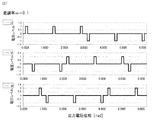
図8、図9は、変調率mが0.8で、パルス数を7パルスから5パルスに三相同時に切り替えた比較例によるインバータ出力電圧を示す図で、特に図8は各相の相電圧を示し、図9は線間電圧(WU)を示す。
この場合、U相の120°(2/3πrad)の位相で周波数指令値Fcが変化し、パルス数決定部13が決定するパルス数Pnumが7から5に変化した。そして、それに応じてスイッチングパターンがU相の120°(2/3πrad)の位相で三相同時に切り替わった。
In order to explain the switching of the number of pulses according to this embodiment, a case where the switching pattern is switched without adjusting the switching timing will be described below as a comparative example.
8 and 9 are diagrams showing inverter output voltages according to a comparative example in which the modulation factor m is 0.8 and the number of pulses is switched from three to five simultaneously, and FIG. FIG. 9 shows the line voltage (WU).
In this case, the frequency command value Fc changed at a phase of 120 ° (2 / 3πrad) of the U phase, and the pulse number Pnum determined by the pulse
図8に示すように、パルス数が7パルスから5パルスに切り替わる時に、U相でパルスが途中でオフになるタイミングと、W相のパルスがオフになるタイミングが近接している。このため図9に示すように、切り替えのタイミングの直後に、WU線間電圧が2倍のスイッチング電圧で変化する。このように、スイッチングパターンの切り替え直後に線間電圧が2倍のスイッチング電圧で変動すると、電流は大きく変動し高調波が発生する。 As shown in FIG. 8, when the number of pulses is switched from 7 pulses to 5 pulses, the timing at which the U-phase pulse is turned off and the timing at which the W-phase pulse is turned off are close to each other. For this reason, as shown in FIG. 9, immediately after the switching timing, the WU line voltage changes at twice the switching voltage. Thus, when the line voltage fluctuates at twice the switching voltage immediately after switching of the switching pattern, the current fluctuates greatly and a harmonic is generated.
そこで、この実施の形態では、所定の時間、例えば最小パルス幅Limの2倍、の間にインバータ4の出力線間電圧が2倍のスイッチング電圧で変化することが無いタイミングでスイッチングパターンの切り替えを行う。
図10、図11は、この実施の形態において、変調率mが0.8で、パルス数を7パルスから5パルスに三相同時に切り替えたインバータ出力電圧を示す図で、特に図10は各相の相電圧を示し、図11は線間電圧を示す。
Therefore, in this embodiment, switching of the switching pattern is performed at a timing at which the output line voltage of the
10 and 11 are diagrams showing inverter output voltages in which the modulation factor m is 0.8 and the number of pulses is switched from 7 pulses to 5 pulses at the same time in this embodiment. In particular, FIG. FIG. 11 shows the line voltage.
この場合、U相の120°(2/3πrad)の位相で周波数指令値Fcが変化し、パルス数決定部13が決定するパルス数Pnumが7から5に変化した。そして、パルス数切替部14は、予め記憶している切替位相、この場合U相の92°を指示する切替指令15を出力し、U相の92°の位相でスイッチングパターンを三相同時に切り替える。
即ち、パルス数決定部13からのパルス数Pnumが7から5に変化しても、切替指令15による切替位相までは7パルスのスイッチングパターンが用いられ、切替位相において、変化後のパルス数である5パルスのスイッチングパターンが、スイッチングパターンテーブル12からゲート発生器16に導出される。
In this case, the frequency command value Fc changed at a phase of 120 ° (2 / 3πrad) of the U phase, and the pulse number Pnum determined by the pulse
That is, even if the pulse number Pnum from the pulse
図10、図11に示すように、スイッチングパターンのパルス数切り替え前後の各相の出力電圧のパルス幅がスイッチング素子6の特性で決まる最小パルス幅Lim以上で、かつ出力線間電圧にも、2倍のスイッチング電圧の電圧変動が発生しない。
このようにパルス数決定部13からのパルス数Pnumが変化しても、所定の時間内でインバータ4の出力線間電圧が2倍のスイッチング電圧で変化することが無いタイミングまで待機させる切替移行期間を設け、スイッチングパターンの切り替えを行う。
As shown in FIGS. 10 and 11, the pulse width of the output voltage of each phase before and after switching the number of pulses of the switching pattern is not less than the minimum pulse width Lim determined by the characteristics of the
In this way, even when the pulse number Pnum from the pulse
これにより、インバータ4によるモータ制御において、モータ負荷運転時や、加減速や電圧上昇/下降時にパルス数の切り替えが発生した場合、スイッチング電圧の2倍以上の線間電圧変動を回避できるため、高調波電圧、サージ電圧の少ない出力電圧を得ることができる。また、パルス数の切り替えに伴う負荷電流変動を少なくでき、低次高調波を低減しつつ負荷に影響を与えないパルス数切り替えが実現できる。
また、パルス数切替を伴うモータ制御において、安定したトルク脈動の少ないモータ制御を実現できる。
As a result, in the motor control by the
In motor control with pulse number switching, stable motor control with less torque pulsation can be realized.
なお、パルス数切り替え時に線間電圧が2倍のスイッチング電圧で変化しない位相は、スイッチングパターンとスイッチング素子6の特性によって決まるため、必ずしも決まった位相にはならない。
Note that the phase at which the line voltage does not change at twice the switching voltage when switching the number of pulses is determined by the switching pattern and the characteristics of the
また上記実施の形態では、パルス数切替部14が切替位相を予め記憶して用いたが、パルス数決定部13からのパルス数Pnumが変化した時に、線間電圧のパルス幅が所定の幅を満たす位相を計算する方法でも良い。また、予め設定された切替位相を、パルス数、変調率毎のスイッチングパターンを記憶しているスイッチングパターンテーブル12に、追加して記憶させても良い。前者は電力変換装置2の制御部10の処理時間に余裕があってメモリが少ない場合、後者は制御部10のメモリに余裕があるが、処理時間に余裕がない場合に有効である。
In the above embodiment, the pulse
なお、実施の形態1ではインバータ4は中性点クランプ式の3レベルインバータとしたが、この限りではないことはいうまでもない。
In the first embodiment, the
実施の形態2.
上記実施の形態1では、スイッチングパターンを切り替えるタイミングを調整したが、この実施の形態2では、切替移行期間においてパルスの調整を行う。パルス数切替部14による動作以外は上記実施の形態1と同様である。
この実施の形態では、パルス数切替部14は、パルス調整手段を有するものとし、パルス数決定部13が決定するパルス数Pnumが変化すると、切替移行期間においてスイッチングパターンのパルスを調整する。
In the first embodiment, the timing for switching the switching pattern is adjusted. In the second embodiment, the pulse is adjusted in the switching transition period. Except for the operation by the pulse
In this embodiment, the pulse
図12は、この発明の実施の形態2によるパルス数切り替えを説明する1相分の電圧波形図である。図に示すように、パルス数を5パルスから3パルスに切り替えるもので、この場合、位相θで周波数指令値Fcが変化し、パルス数決定部13が決定するパルス数Pnumが5から3に変化している。これにより、5パルス用のスイッチングパターン21(th1a、th2a、th3a、th4a、th5a)から3パルス用のスイッチングパターン22(th1b、th2b、th3b)に切り替わるが、切替移行期間において調整パターン23を用いる。
FIG. 12 is a voltage waveform diagram for one phase for explaining the pulse number switching according to the second embodiment of the present invention. As shown in the figure, the pulse number is switched from 5 pulses to 3 pulses. In this case, the frequency command value Fc changes with the phase θ, and the pulse number Pnum determined by the pulse
図12に示すように、調整パターン23は、3パルス用のスイッチングパターン22を変形したパルスパターンと、ダミーパルス24とで構成され、変形したパルスパターンは、ダミーパルス24による増加分を解消する為の削除パルス25を除いたパターンである。
この場合、切り替え時の位相θの前後で出力すべき相電圧のレベルが異なり、パルス幅が最小パルス幅Limを確保できなくなるため、thxでオフするダミーパルス24を発生させて切り替え時のパルス幅Lを、最小パルス幅Limより長くする。また、ダミーパルス24によるパルス増加分を解消する為、3パルス用のスイッチングパターン22(th1b、th2b、th3b)のパルス幅を縮めたパルスパターン(th1x、th2b、th3b)を用いる。
As shown in FIG. 12, the
In this case, since the level of the phase voltage to be output differs before and after the phase θ at the time of switching, and the pulse width cannot secure the minimum pulse width Lim, a
なお、削除パルス25の幅は、ダミーパルス24のパルス幅と同じにしても良いし、あるいは変調率mがパルス数切り替え前後で同じになるように演算して求めても良い。変調率mを同じにする場合は、上記式(3)(4)の第1条件式を利用して求めることが可能である。
The width of the
以上のようなパルス数の切り替えによると、加速/減速運転時や電圧振幅が上昇/下降してスイッチングパターンの変化が早くて、特定位相での切り替えでは遅い場合や、パルス数切り替え前後のスイッチング位相の変化が大きい場合にも、切り替え前後のスイッチング位相の変化による変調率の変動や電圧高調波の発生、及びそれによる電流変動を抑制することができる。即ち、パルス数の切り替えに伴う負荷電流変動を少なくでき、低次高調波を低減しつつ負荷に影響を与えないパルス数切り替えが実現できる。
また、パルス数切替を伴うモータ制御において、安定したトルク脈動の少ないモータ制御を実現できる。
When switching the number of pulses as described above, the switching pattern changes quickly during acceleration / deceleration operation or when the voltage amplitude increases / decreases, and the switching phase changes before or after switching the number of pulses. Even when there is a large change, the fluctuation of the modulation factor and the generation of voltage harmonics due to the change of the switching phase before and after the switching, and the current fluctuation caused thereby can be suppressed. That is, the load current fluctuation accompanying the switching of the number of pulses can be reduced, and the switching of the number of pulses that does not affect the load while reducing the low-order harmonics can be realized.
In motor control with pulse number switching, stable motor control with less torque pulsation can be realized.
実施の形態3.
上記実施の形態2では、切替移行期間においてスイッチングパターンのパルスを調整したが、この実施の形態3では、切替用スイッチングパターンを予め記憶し、切替移行期間において切替用スイッチングパターンを用いる。パルス数切替部14による動作以外は上記実施の形態1と同様である。
この実施の形態では、パルス数切替部14は、出力電圧の低次高調波を低減した切替用スイッチングパターンを、パルス数別に変調率mの大きさに応じて記憶する手段(第2の記憶手段)を備えるものとする。
In the second embodiment, the switching pattern pulse is adjusted in the switching transition period. However, in the third embodiment, the switching pattern is stored in advance, and the switching pattern is used in the switching transition period. Except for the operation by the pulse
In this embodiment, the pulse
図13は、この発明の実施の形態3によるパルス数切り替えを説明する1相分の電圧波形図である。図に示すように、パルス数を5パルスから3パルスに切り替えるもので、この場合、パルス数決定部13が決定するパルス数Pnumが5から3に変化すると、5パルス用のスイッチングパターン21(th1a、th2a、th3a、th4a、th5a)から一旦、切替用スイッチングパターン26(th1、th2、th3、th4、th5)に切り替え、その後、例えば1周期後に3パルス用のスイッチングパターン22(th1b、th2b、th3b)に切り替える。
なお、3パルスから5パルスに切り替える時は、逆の処理をすれば良い。3パルス用のスイッチングパターン22と5パルス用のスイッチングパターン21との間の切替用スイッチングパターン26は5パルス構成で、双方のスイッチングパターン21、22の位相に近く、かつ低次高調波を低減したパルス数切り替え時専用のスイッチングパターンである。
FIG. 13 is a voltage waveform diagram for one phase for explaining the pulse number switching according to the third embodiment of the present invention. As shown in the figure, the pulse number is switched from 5 pulses to 3 pulses. In this case, when the pulse number Pnum determined by the pulse
When switching from 3 pulses to 5 pulses, the reverse process may be performed. The switching
切替用スイッチングパターン26(th1、th2、th3、th4、th5)は、次式(5)で求められる。
(4/π)・(costh1−costh2+costh3−costh4+costh5)=m
cos5th1−cos5th2+cos5th3−cos5th4+cos5th5=0
cos7th1−cos7th2+cos7th3−cos7th4+cos7th5=0
│th2b−th4│≦wdh
│th1a−th1│≦wdh ・・・(5)
The switching pattern for switching 26 (th1, th2, th3, th4, th5) is obtained by the following equation (5).
(4 / π) · (costh1-costh2 + costh3-costh4 + costh5) = m
cos5th1-cos5th2 + cos5th3-cos5th4 + cos5th5 = 0
cos7th1-cos7th2 + cos7th3-cos7th4 + cos7th5 = 0
│th2b-th4│ ≦ wdh
│th1a-th1│ ≦ wdh (5)
式(5)中のwdhは、切替用スイッチングパターン26の、3パルス用スイッチングパターン22、5パルス用スイッチングパターン21からのスイッチング位相の差の上限であり、切り替え前後のスイッチングパターンのパルス幅の1/2や、最小パルス幅Lminの1/2などで、変調率mによって変えても良い。
なお、上記式(5)では、11次と13次の高調波を低減せずに5次と7次の高調波を低減する条件としたが、逆に11次と13次の高調波のみを低減しても良い。また、変調率mによっては低減する高調波の数を増減してもよい。
In formula (5), wdh is the upper limit of the difference in switching phase of the
In the above equation (5), the fifth and seventh harmonics are reduced without reducing the eleventh and thirteenth harmonics. Conversely, only the eleventh and thirteenth harmonics are used. It may be reduced. Further, the number of harmonics to be reduced may be increased or decreased depending on the modulation factor m.
以上のようなパルス数の切り替えにより、加速/減速運転時や電圧振幅が上昇/下降してスイッチングパターンの変化が早くて、特定位相での切り替えでは遅い場合や、パルス数切り替え前後のスイッチング位相の変化が大きい場合にも、切り替え前後のスイッチング位相の変化による変調率の変動や電圧高調波の発生、及びそれによる電流変動を抑制することができる。この場合、パルス数の切り替えに伴う電圧変動、電流変動や高調波の発生を上記実施の形態2よりもさらに抑制でき、効率の良い安定した制御が求められる場合に有効である。 By switching the number of pulses as described above, the switching pattern changes quickly during acceleration / deceleration operation or when the voltage amplitude increases / decreases, and switching at a specific phase is slow, or the switching phase before and after switching the number of pulses Even when the change is large, it is possible to suppress the variation of the modulation factor and the generation of voltage harmonics due to the change of the switching phase before and after the switching, and the current fluctuation caused by the variation. In this case, the occurrence of voltage fluctuation, current fluctuation and harmonics accompanying switching of the number of pulses can be further suppressed as compared with the second embodiment, which is effective when efficient and stable control is required.
上記実施の形態1〜3は、それぞれ異なる手法でパルス数の切り替えを行うものであるが、パルス数切替部14が、上記実施の形態1によるパルス数の切り替えを行う第1の切替手段と、上記実施の形態2によるパルス数の切り替えを行う第2の切替手段と、上記実施の形態3によるパルス数の切り替えを行う第3の切替手段とを備え、さらに選択手段を有して適宜選択して用いるようにしても良い。その場合、第1の切替手段と第2、あるいは第3の切替手段とを組み合わせる等、複数の切替手段を組み合わせて用いることも可能である。
In the first to third embodiments, the number of pulses is switched by different methods. The pulse
これにより、最適な切替方法を選択してパルス数を切り替えることができる。例えば変調率や出力電圧振幅Vpに関係なく、モータ負荷電流が多い場合や、一定速度(=電圧)運転の場合は、電圧の変動による電流の一時的な変動が大きくなるが、このような場合には、パルス数の切り替えを切替前後のパルスパターンにより決まる線間電圧が2倍のスイッチング電圧にならない位相で切り替えるのが有効であり、第1の切替手段を選択する。 また、加速/減速運転時や電圧振幅が上昇/下降してスイッチングパターンの変化が早くて、特定位相での切り替えでは遅い場合や、パルス数切り替え前後のスイッチング位相の変化が大きい場合には、第2あるいは第3の切替手段を選択する。 Thereby, the optimal switching method can be selected and the number of pulses can be switched. For example, when the motor load current is large or the motor is operated at a constant speed (= voltage) regardless of the modulation factor or the output voltage amplitude Vp, the temporary fluctuation of the current due to the fluctuation of the voltage becomes large. For this, it is effective to switch the number of pulses at a phase where the line voltage determined by the pulse pattern before and after the switching does not become a double switching voltage, and the first switching means is selected. Also, when acceleration / deceleration operation or when the voltage amplitude increases / decreases and the switching pattern changes quickly and switching at a specific phase is slow, or when the switching phase changes significantly before and after switching the number of pulses, 2 or 3rd switching means is selected.
実施の形態4.
次に、この発明の実施の形態4による電力変換装置を説明する。
図14は、この発明の実施の形態1による電力変換装置の構成を示す図である。図14に示すように、電力変換装置32は、インバータ34とインバータ34を制御する制御部40とを備えて、直流電圧源31a〜31cの直流電力を交流電力に変換してモータ3に供給する。
インバータ34は、各相の直流電圧源31a〜31cの電圧を分圧する2直列のコンデンサ5a、5bと、それぞれダイオードが逆並列接続されたIGBT等から成る複数のスイッチング素子6およびクランプダイオード7を備えた中性点クランプ式の3レベルインバータの2つのレグ(Aレグ8a、Bレグ8b)を直列接続した5レベルインバータとを3相分用意したものである。そして、スイッチング素子6のスイッチング動作によって直流電圧源31a〜31cの電圧を任意の大きさ及び周波数の出力電圧に変換する。
Next, a power converter according to
FIG. 14 is a diagram showing a configuration of the power conversion device according to
The
制御部40は、上記実施の形態1と同様に、変調率mを演算する変調率演算器11と、インバータ34の周波数指令値Fcからパルス数Pnumを決定するパルス数決定部13とを備える。この場合のパルス数とは、各レグ8a、8b毎に出力する半周期あたりのパルス数で、2つのレグ8a、8bでは2倍となる。また制御部40は、パルス数別に変調率mの大きさに応じて予め決定されたスイッチングパターンth1a、th2a、th3a、・・th1b、th2b、th3b、・・を記憶する記憶手段としてのスイッチングパターンテーブル42を備える。なお、(th1a、th2a、th3a、・・)は、Aレグ8aに対するスイッチングパターンであり、(th1b、th2b、th3b、、・・)は、Bレグ8bに対するスイッチングパターンである。即ち、スイッチングパターンテーブル42はレグ8a、8b毎に異なるスイッチングパターンを記憶し、2種のスイッチングパターンを組み合わせて2レグ分のスイッチングパターンとする。
Similarly to the first embodiment, the
さらに制御部40は、パルス数決定部13からのパルス数Pnumが変化したときに、PWM制御のパルス数を切り替えるパルス数切替手段としてのパルス数切替部44と、インバータ34の各スイッチング素子6を駆動制御するゲート信号47を生成するゲート信号生成部としてのゲート発生器46とを備える。
Further, the
次に動作を説明する。
上記実施の形態1と同様に、変調率演算器11は、インバータ出力電圧の相電圧振幅Vpと直流電圧源1の電圧Vdcとから変調率mを演算し、パルス数決定部13は、インバータ4の周波数指令値Fcに応じてPWM制御における半周期あたりのパルス数Pnumを決定する。
スイッチングパターンテーブル42では、パルス数Pnum別に、変調率mの大きさ毎に出力電圧の低次高調波を低減できるスイッチングパターンを記憶し、パルス数決定部13からのパルス数Pnumと、変調率演算器11からの変調率mとに基づいて、スイッチングパターンを導出する。
Next, the operation will be described.
As in the first embodiment, the
In the switching pattern table 42, a switching pattern that can reduce the lower harmonic of the output voltage is stored for each pulse number Pnum for each magnitude of the modulation factor m, and the pulse number Pnum from the pulse
また、周波数指令値Fcによって決まるパルス数Pnumが変化すると、スイッチングパターンテーブル42から導出されるスイッチングパターンも切り替わるものであるが、パルス数切替部44では切替移行期間を設けて、各レグ間でスイッチングパターンの切り替え位相をずらす。この場合、パルス数Pnumが変化すると、まずAレグ8aに対するスイッチングパターンのみを切り替え、所定の切替移行期間終了時に切替指令45によりBレグ8bに対するスイッチングパターンも切り替える。
Further, when the number of pulses Pnum determined by the frequency command value Fc changes, the switching pattern derived from the switching pattern table 42 is also switched. However, the pulse
次に、スイッチングパターンについて説明する。
図15(a)は、PWM制御の一相分のインバータ出力電圧を示す図である。図15(b)はAレグ8aの出力電圧、図15(c)はBレグ8bの出力電圧を示し、Aレグ8aの出力電圧とBレグ8bの出力電圧とを合成したものが、図15(a)で示す一相分のインバータ出力電圧となる。この場合、直列接続された2レグ分の3レベルインバータがそれぞれ基本波の1/4周期に3回スイッチングして、パルス数を3×2とする。
Next, the switching pattern will be described.
FIG. 15A is a diagram illustrating an inverter output voltage for one phase of PWM control. FIG. 15B shows the output voltage of the
従来方式では、パルス数が3×2の場合、スイッチングパターンth1a、th2a、th3a、th1b、th2b、th3bは、特定の低次の高調波を低減するように次式(6)で求めていた。式(6)では理論的には5次、7次、11次、13次の高調波を低減し、2レグ分の3レベルインバータに基本波を等しく分担するようにしている。
(4/π)・(costh1a−costh2a+costh3a)=m
(4/π)・(costh1b−costh2b+costh3b)=m
cos5th1a−cos5th2a+cos5th3a
+cos5th1b−cos5th2b+cos5th3b=0
cos7th1a−cos7th2a+cos7th3a
+cos7th1b−cos7th2b+cos7th3b=0
cos11th1a−cos11th2a+cos11th3a
+cos11th1b−cos11th2b+cos11th3b=0
cos13th1a−cos13th2a+cos13th3a
+cos13th1b−cos13th2b+cos13th3b=0
・・・(6)
In the conventional method, when the number of pulses is 3 × 2, the switching patterns th1a, th2a, th3a, th1b, th2b, and th3b are obtained by the following equation (6) so as to reduce specific low-order harmonics. In equation (6), the fifth, seventh, eleventh, and thirteenth harmonics are theoretically reduced, and the fundamental wave is equally shared by the three-level inverters for two legs.
(4 / π) · (costh1a−costh2a + costh3a) = m
(4 / π) · (costh1b−costh2b + costh3b) = m
cos5th1a-cos5th2a + cos5th3a
+ Cos5th1b-cos5th2b + cos5th3b = 0
cos7th1a-cos7th2a + cos7th3a
+ Cos7th1b-cos7th2b + cos7th3b = 0
cos11th1a-cos11th2a + cos11th3a
+ Cos11th1b-cos11th2b + cos11th3b = 0
cos13th1a-cos13th2a + cos13th3a
+ Cos13th1b-cos13th2b + cos13th3b = 0
... (6)
しかし低変調率になるにつれて、スイッチング位相のth1aとth2aとの間隔、th1bとth2bとの間隔が順番に短くなって、パルス幅が狭くなり、スイッチング素子の特性によってはスイッチングに追従できない場合がある。例えば、大容量インバータのスイッチング素子として用いられるGTOなどは、要求されるパルス幅が比較的大きく、スイッチングに追従できずに出力電圧が大きく歪んでしまう。 However, as the modulation factor becomes lower, the interval between the switching phases th1a and th2a and the interval between th1b and th2b become shorter in sequence, the pulse width becomes narrower, and switching may not be able to follow depending on the characteristics of the switching element. . For example, a GTO used as a switching element of a large-capacity inverter has a relatively large required pulse width and cannot follow the switching, and the output voltage is greatly distorted.
そこで、この実施の形態では低変調率、例えば変調率mが0.3以下では、スイッチングパターンth1a、th2a、th3a、th1b、th2b、th3bを、次式(7)で求める。 Therefore, in this embodiment, when the modulation factor is low, for example, the modulation factor m is 0.3 or less, the switching patterns th1a, th2a, th3a, th1b, th2b, th3b are obtained by the following equation (7).
(4/π)・(costh1a−costh2a+costh3a)=m
(4/π)・(costh1b−costh2b+costh3b)=m
cos5th1a−cos5th2a+cos5th3a
+cos5th1b−cos5th2b+cos5th3b=0
cos7th1a−cos7th2a+cos7th3a
+cos7th1b−cos7th2b+cos7th3b=0
(th2a−th1a)≧Lim
(th2b−th1b)≧Lim ・・・(7)
(4 / π) · (costh1a−costh2a + costh3a) = m
(4 / π) · (costh1b−costh2b + costh3b) = m
cos5th1a-cos5th2a + cos5th3a
+ Cos5th1b-cos5th2b + cos5th3b = 0
cos7th1a-cos7th2a + cos7th3a
+ Cos7th1b-cos7th2b + cos7th3b = 0
(Th2a-th1a) ≧ Lim
(Th2b−th1b) ≧ Lim (7)
式(7)では、高調波低減の条件を緩和して5次、7次の高調波のみを低減し、かつ最小パルス幅Limを確保できるスイッチングパターンを得ることができる。最小パルス幅Limは、スイッチング素子6の特性において決まる最小のパルス幅であり、スイッチング素子6が追従するのに必要なパルス幅である。この場合、Lim=0.116とする。
なお、パターンの求め方はこの限りではないことは言うまでもない。
In Expression (7), it is possible to obtain a switching pattern that relaxes the harmonic reduction condition, reduces only the fifth and seventh harmonics, and can secure the minimum pulse width Lim. The minimum pulse width Lim is the minimum pulse width determined by the characteristics of the
It goes without saying that the method of obtaining the pattern is not limited to this.
式(7)により求めたスイッチングパターンを図16に示す。図16(a)はAレグ8aのスイッチングパターンth1a、th2a、th3aを示し、図16(b)はBレグ8bのスイッチングパターンth1b、th2b、th3bを示す。
ただし、スイッチングパターンテーブル42が記憶するスイッチングパターンは、変調率mを0.01刻みとし、その間は線形補完により求めて用いる。
同様にしてパルス数が5×2、7×2、9×2・・・についても、低変調率においてスイッチング素子の特性で決まる最小パルス幅Limを確保し、かつ低次高調波を低減できるスイッチングパターン、即ち出力電圧を得ることができる。
FIG. 16 shows a switching pattern obtained by the equation (7). FIG. 16A shows switching patterns th1a, th2a and th3a of the
However, the switching pattern stored in the switching pattern table 42 is obtained by using a linear interpolation in which the modulation factor m is set in increments of 0.01.
Similarly, for the number of pulses of 5 × 2, 7 × 2, 9 × 2,..., Switching that can secure a minimum pulse width Lim determined by the characteristics of the switching element at a low modulation rate and reduce low-order harmonics. A pattern, that is, an output voltage can be obtained.
次に、パルス数の切り替えについて説明する。
この実施の形態では、上述したように、周波数指令値Fcによって決まるパルス数Pnumが変化した時に、パルス数切替部44が、各レグ間でスイッチングパターンの切り替え位相をずらす。
図17は、この発明の実施の形態4によるパルス数切り替えを説明する2レグ分の電圧波形図である。この2レグ分の出力電圧を合成したものが、一相分の出力電圧となる。
Next, switching of the number of pulses will be described.
In this embodiment, as described above, when the pulse number Pnum determined by the frequency command value Fc changes, the pulse
FIG. 17 is a voltage waveform diagram for two legs for explaining the pulse number switching according to the fourth embodiment of the present invention. The output voltage for one phase is obtained by combining the output voltages for the two legs.
図17に示すように、パルス数を5×2パルスから7×2パルスに切り替える。この場合、位相θで周波数指令値Fcが変化して、パルス数決定部13が決定するパルス数Pnumが5から7に変化する。これにより、Aレグ8aに対する5パルス用のスイッチングパターンから7パルス用のスイッチングパターンに切り替える。そして、所定のずらし位相Δθ分の切替移行期間において、Aレグ8aは7パルス用のスイッチングパターンを用いて駆動し、Bレグ8bは5パルス用のスイッチングパターンを用いて駆動する。切替移行期間が終了する位相θaにおいて、Bレグ8bに対する5パルス用のスイッチングパターンから7パルス用のスイッチングパターンに切り替える。
この場合、ずらし位相Δθは、最小パルス幅Lim(=0.116)の1/2(=0.058)とした。
As shown in FIG. 17, the number of pulses is switched from 5 × 2 pulses to 7 × 2 pulses. In this case, the frequency command value Fc changes at the phase θ, and the pulse number Pnum determined by the pulse
In this case, the shift phase Δθ is set to 1/2 (= 0.058) of the minimum pulse width Lim (= 0.116).
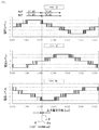
この実施の形態によるパルス数の切り替えの効果を説明するために、まず、2レグ8a、8bのスイッチングパターンを同時に切り替える場合を、比較例として以下に説明する。
図18、図19は、変調率mが0.9で、パルス数を5×2パルスから7×2パルスに三相同時、かつ2レグ8a、8bで同時に切り替えた比較例によるインバータ出力電圧を示す図で、特に図18は各相の相電圧を示し、図19は線間電圧を示す。
この場合、U相の120°(2/3πrad)の位相で周波数指令値Fcが変化し、パルス数決定部13が決定するパルス数Pnumが5から7に変化した。そして、それに応じてスイッチングパターンがU相の120°(2/3πrad)の位相で切り替わる。
In order to explain the effect of switching the number of pulses according to this embodiment, the case where the switching patterns of the two
18 and 19 show the inverter output voltage according to the comparative example in which the modulation factor m is 0.9, the number of pulses is switched from 5 × 2 pulses to 7 × 2 pulses at the same time in three phases and simultaneously in the two
In this case, the frequency command value Fc changed at a phase of 120 ° (2 / 3πrad) of the U phase, and the pulse number Pnum determined by the pulse
図18に示すようにAレグ8aとBレグ8bとを同時にパルス数を切り替えると、切り替えのタイミングで、U相の電圧レベルが1から2へ変化し、W相の電圧レベルが−1から−2に変化する。このため図19に示すように、線間電圧WUの電圧レベルが−2から−4に変化し、2倍のスイッチング電圧による電圧変動が発生する。この電圧変動は、マイナス側のピーク電圧のレベルで発生しているため、負荷がある場合、電流変動も大きく、モータ3への影響が大きい。
As shown in FIG. 18, when the number of pulses is switched simultaneously between the
図20、図21は、この実施の形態によるパルス数切り替えにおけるインバータ出力電圧を示す図で、特に図20は各相の相電圧を示し、図21は線間電圧を示す。この場合も、上記比較例と同様に、変調率mが0.9で、パルス数を5×2パルスから7×2パルスに切り替え、U相の120°(2/3πrad)の位相で周波数指令値Fcが変化し、パルス数決定部13が決定するパルス数Pnumが5から7に変化した。
図17で説明したように、位相θ(U相の120°)で周波数指令値Fcが変化してパルス数決定部13が決定するパルス数Pnumが5から7に変化すると、Aレグ8aに対する5パルス用のスイッチングパターンから7パルス用のスイッチングパターンに切り替える。そして、最小パルス幅Lim(=0.116)の1/2(=0.058)である、ずらし位相Δθ経過後の位相θaにおいて、Bレグ8bに対する5パルス用のスイッチングパターンから7パルス用のスイッチングパターンに切り替える。
20 and 21 are diagrams showing the inverter output voltage in the pulse number switching according to this embodiment. In particular, FIG. 20 shows the phase voltage of each phase, and FIG. 21 shows the line voltage. In this case as well, as in the above comparative example, the modulation factor m is 0.9, the number of pulses is switched from 5 × 2 pulses to 7 × 2 pulses, and the frequency command is set at a phase of 120 ° (2 / 3πrad) of the U phase. The value Fc changed, and the pulse number Pnum determined by the pulse
As described with reference to FIG. 17, when the frequency command value Fc changes at the phase θ (120 ° of the U phase) and the pulse number Pnum determined by the pulse
この実施の形態では、図20に示すように、三相の電圧変化が同時に±逆の方向に変化せず、このため図21に示すように、線間電圧において2倍のスイッチング電圧による電圧変動が発生しない。 In this embodiment, as shown in FIG. 20, the three-phase voltage change does not change in the opposite direction at the same time. Therefore, as shown in FIG. 21, the voltage fluctuation caused by the double switching voltage in the line voltage. Does not occur.
なお、上記実施の形態では、インバータ34の各相の5レベルインバータを2つのレグ8a、8bを直列接続して構成したが、3以上のレグを直列接続しても良く、パルス数の切り替えの際は、各レグ間で位相をずらして切り替える。
In the above embodiment, the five-level inverter of each phase of the
以上のようにインバータ34の各相の5レベルインバータを構成する3レベルの2つのレグ8a、8bのスイッチングパターンにおけるパルス数をレグ間で位相をずらして順次切り替えることにより、相電圧変動、線間電圧変動を小さくし、これにより電流変動、トルク脈動が少なく安定した制御状態を保つことができる。
また、インバータ34が5レベル以上のマルチレベルインバータになり、インバータ34の出力電圧波形が複数のレグ8a、8bのスイッチングパターンの組み合わせになって複雑化しても、メモリや処理負担が少なく容易に制御でき、かつパルス数の切り替え前後で変調率の変動がないため、パルス数の切り替えによる電圧波形の変動および電流変動が小さく、モータ制御が安定して行える。
As described above, by sequentially switching the number of pulses in the switching pattern of the three-level two
Further, even if the
なお、この実施の形態による回路構成の5レベルインバータであるインバータ34に、3レベルの2つのレグ8a、8bのスイッチングパターンの組み合わせを考慮して、上記実施の形態1〜3によるパルス切り替えを適用することもできる。
さらにまた、パルス数切替部44が、上記各実施の形態1〜4によるパルス切り替えを実現する切り替え手段を全て有して、最適な切り替え手段を選択して用いても良い。
Note that the pulse switching according to the above-described first to third embodiments is applied to the
Furthermore, the pulse
また、この実施の形態4では各相の5レベルインバータは、中性点クランプ式の3レベルインバータの2レグ分を直列接続したものとしたが、この限りではない。 In the fourth embodiment, the five-level inverter of each phase is obtained by connecting two legs of a neutral-point clamped three-level inverter in series, but this is not restrictive.
また、この発明は、その発明の範囲内において、各実施の形態を自由に組み合わせたり、各実施の形態を適宜、変形、省略することが可能である。 Further, within the scope of the present invention, the present invention can be freely combined with each other, and each embodiment can be appropriately modified or omitted.
1 直流電圧源、2 電力変換装置、4 インバータ、6 スイッチング素子、
8a,8b レグ、10 制御部、11 変調率演算器、
12 スイッチングパターンテーブル、13 パルス数決定部、14 パルス数切替部、15 切替指令、16 ゲート発生器、17 ゲート信号、23 調整パターン、
24 ダミーパルス、25 削除パルス、26 切替用スイッチングパターン、
31a〜31c 直流電圧源、32 電力変換装置、34 インバータ、40 制御部、
42 スイッチングパターンテーブル、44 パルス数切替部、45 切替指令、
46 ゲート発生器、47 ゲート信号、Δθ ずらし位相。
1 DC voltage source, 2 power converter, 4 inverter, 6 switching element,
8a, 8b leg, 10 control unit, 11 modulation factor calculator,
12 switching pattern table, 13 pulse number determination unit, 14 pulse number switching unit, 15 switching command, 16 gate generator, 17 gate signal, 23 adjustment pattern,
24 dummy pulse, 25 deletion pulse, 26 switching pattern for switching,
31a to 31c DC voltage source, 32 power converter, 34 inverter, 40 control unit,
42 switching pattern table, 44 pulse number switching unit, 45 switching command,
46 Gate generator, 47 gate signal, Δθ shift phase.
Claims (9)
上記制御部は、
上記出力電圧と上記直流電圧源の電圧とに基づいて変調率を演算する変調率演算手段と、
上記スイッチング素子のPWM制御における半周期あたりのパルス数を上記インバータに設定される出力周波数に基づいて決定するパルス数決定手段と、
上記出力電圧の低次高調波を低減し、かつ上記スイッチング素子の特性により決まる最小パルス幅を確保したスイッチングパターンを、パルス数別に変調率の大きさに応じて記憶する記憶手段と、
上記変調率演算手段からの変調率と、上記パルス数決定手段からのパルス数とに基づいて上記記憶手段からのスイッチングパターンを用い、上記スイッチング素子を駆動するゲート信号を生成するゲート信号生成部と、
上記パルス数決定手段からのパルス数が変化したとき、上記ゲート信号生成部が用いる上記スイッチングパターンを、変化後のパルス数に基づくスイッチングパターンに切り替える際に、上記出力電圧の変動を抑制する切替移行期間を設けるパルス数切替手段とを備えたことを特徴とする電力変換装置。 An inverter that has a switching element and converts the voltage of the DC voltage source into an output voltage of an arbitrary magnitude and frequency, and a control unit that PWM-controls the switching element,
The control unit
A modulation factor calculating means for calculating a modulation factor based on the output voltage and the voltage of the DC voltage source;
Pulse number determination means for determining the number of pulses per half cycle in PWM control of the switching element based on the output frequency set in the inverter;
Storage means for storing low-order harmonics of the output voltage and storing a switching pattern that secures a minimum pulse width determined by the characteristics of the switching element according to the magnitude of the modulation rate for each number of pulses;
A gate signal generating unit that generates a gate signal for driving the switching element using a switching pattern from the storage unit based on the modulation rate from the modulation rate calculating unit and the number of pulses from the pulse number determining unit; ,
When the number of pulses from the number-of-pulse determining means changes, the switching transition that suppresses fluctuations in the output voltage when the switching pattern used by the gate signal generation unit is switched to the switching pattern based on the number of pulses after the change. A power conversion device comprising a pulse number switching means for providing a period.
第1〜第3の切替手段の少なくとも1つを選択して用いる選択手段とを備え、
上記第1の切替手段は、上記パルス数決定手段からのパルス数が変化したとき、上記最小パルス幅を確保でき、かつ所定の時間内に出力線間電圧が2倍のスイッチング電圧で変化することが無いタイミングまで待って、変化後のパルス数に基づくスイッチングパターンに切り替え、該タイミングまで切り替え前状態を継続させる期間を上記切替移行期間とするものであり、
上記第2の切替手段は、上記最小パルス幅を確保するようにダミーパルスを発生させ、かつ該ダミーパルスによるパルス増加分を解消するパルス調整手段を備え、上記パルス数決定手段からのパルス数が変化した後の上記切替移行期間において、変化後のパルス数に基づくスイッチングパターンを上記パルス調整手段により調整して、上記ゲート信号生成部が用いる上記スイッチングパターンとするものであり、
上記第3の切替手段は、上記出力電圧の低次高調波を低減した切替用スイッチングパターンを、パルス数別に変調率の大きさに応じて記憶する第2の記憶手段を備え、上記パルス数決定手段からのパルス数が変化した後の上記切替移行期間において、上記第2の記憶手段からの上記切替用スイッチングパターンを、上記ゲート信号生成部が用いる上記スイッチングパターンとするものであることを特徴とする請求項1に記載の電力変換装置。 The pulse number switching means includes a first switching means, a second switching means, a third switching means, and a selecting means for selecting and using at least one of the first to third switching means. Prepared,
The first switching means can ensure the minimum pulse width when the number of pulses from the number-of-pulses determining means changes, and the output line voltage changes at twice the switching voltage within a predetermined time. Wait until the timing without, switch to the switching pattern based on the number of pulses after the change, the period to continue the state before switching until the timing is the switching transition period,
The second switching means includes a pulse adjusting means for generating a dummy pulse so as to secure the minimum pulse width, and canceling the pulse increase due to the dummy pulse, and the number of pulses from the pulse number determining means is In the switching transition period after the change, the switching pattern based on the number of pulses after the change is adjusted by the pulse adjustment means to be the switching pattern used by the gate signal generation unit,
The third switching means includes second storage means for storing a switching pattern for switching in which lower-order harmonics of the output voltage are reduced according to the modulation factor according to the number of pulses, and determining the number of pulses. In the switching transition period after the number of pulses from the means changes, the switching pattern for switching from the second storage means is the switching pattern used by the gate signal generator. The power conversion device according to claim 1.
上記記憶手段は、上記レグ毎に上記スイッチングパターンを記憶し、
上記パルス数切替手段は、上記パルス数決定手段からのパルス数が変化したとき、上記ゲート信号生成部が用いる上記スイッチングパターンを、変化後のパルス数に基づくスイッチングパターンに切り替える位相を上記各レグ間でずらし、全レグの切り替え終了までの期間を上記切替移行期間とすることを特徴とする請求項1に記載の電力変換装置。 The above-mentioned inverter is configured by connecting two or more legs of a neutral-point clamped three-level inverter in series to form one phase.
The storage means stores the switching pattern for each leg,
When the number of pulses from the number-of-pulses determining unit changes, the number-of-pulses switching unit switches a phase for switching the switching pattern used by the gate signal generation unit to a switching pattern based on the number of pulses after the change between the legs. The power conversion device according to claim 1, wherein a period until the end of switching of all legs is set as the switching transition period.
Priority Applications (1)
| Application Number | Priority Date | Filing Date | Title |
|---|---|---|---|
| JP2013010701A JP5892955B2 (en) | 2013-01-24 | 2013-01-24 | Power converter |
Applications Claiming Priority (1)
| Application Number | Priority Date | Filing Date | Title |
|---|---|---|---|
| JP2013010701A JP5892955B2 (en) | 2013-01-24 | 2013-01-24 | Power converter |
Publications (2)
| Publication Number | Publication Date |
|---|---|
| JP2014143831A true JP2014143831A (en) | 2014-08-07 |
| JP5892955B2 JP5892955B2 (en) | 2016-03-23 |
Family
ID=51424664
Family Applications (1)
| Application Number | Title | Priority Date | Filing Date |
|---|---|---|---|
| JP2013010701A Active JP5892955B2 (en) | 2013-01-24 | 2013-01-24 | Power converter |
Country Status (1)
| Country | Link |
|---|---|
| JP (1) | JP5892955B2 (en) |
Cited By (24)
| Publication number | Priority date | Publication date | Assignee | Title |
|---|---|---|---|---|
| WO2016104370A1 (en) * | 2014-12-24 | 2016-06-30 | 三菱電機株式会社 | Power conversion device |
| JP2016208810A (en) * | 2015-04-23 | 2016-12-08 | パナソニックIpマネジメント株式会社 | Power converter |
| JP2016220325A (en) * | 2015-05-15 | 2016-12-22 | 株式会社デンソー | Control device for multilevel inverter |
| JP2017147891A (en) * | 2016-02-18 | 2017-08-24 | 株式会社デンソー | Inverter control device |
| US20180079194A1 (en) * | 2015-03-18 | 2018-03-22 | Riken Technos Corporation | Hard coat laminated film |
| US10461681B2 (en) | 2016-02-24 | 2019-10-29 | Denso Corporation | Inverter control device |
| WO2020044890A1 (en) * | 2018-08-30 | 2020-03-05 | 日立オートモティブシステムズ株式会社 | Inverter device |
| US10596739B2 (en) | 2015-03-18 | 2020-03-24 | Riken Technos Corporation | Molded body |
| US10809418B2 (en) | 2015-03-18 | 2020-10-20 | Riken Technos Corporation | Anti-glare hard coat laminated film |
| US10816700B2 (en) | 2015-12-08 | 2020-10-27 | Riken Technos Corporation | Hard coat layered film |
| WO2020261556A1 (en) * | 2019-06-28 | 2020-12-30 | 三菱電機株式会社 | Power conversion apparatus and driving method for power conversion apparatus |
| WO2021014690A1 (en) * | 2019-07-23 | 2021-01-28 | 株式会社明電舎 | Power converter control system using fixed pulse pattern, and control method |
| JP2021029092A (en) * | 2019-08-13 | 2021-02-25 | 株式会社明電舎 | Controller of power converter and control method of power converter |
| JP2021072679A (en) * | 2019-10-30 | 2021-05-06 | 株式会社明電舎 | Power conversion system |
| CN113097986A (en) * | 2021-03-31 | 2021-07-09 | 国网内蒙古东部电力有限公司电力科学研究院 | Protection method, device and system for primary harmonic elimination device of distribution network voltage transformer |
| US11065852B2 (en) | 2015-03-18 | 2021-07-20 | Riken Technos Corporation | Adhesive film |
| US11065851B2 (en) | 2015-03-18 | 2021-07-20 | Riken Technos Corporation | Multilayer hard coating film |
| US11241866B2 (en) | 2015-11-25 | 2022-02-08 | Riken Technos Corporation | Door body |
| US11352473B2 (en) | 2015-03-18 | 2022-06-07 | Riken Technos Corporation | Hard coat laminated film and method for producing same |
| US11407870B2 (en) | 2016-09-14 | 2022-08-09 | Riken Technos Corporation | Hard coat laminated film |
| US11433651B2 (en) | 2015-03-18 | 2022-09-06 | Riken Technos Corporation | Hard coat laminated film |
| US11639428B2 (en) | 2016-11-25 | 2023-05-02 | Riken Technos Corporation | Hardcoat multilayer film |
| JP7347111B2 (en) | 2019-10-17 | 2023-09-20 | 日産自動車株式会社 | Power converter control method and power converter control device |
| US11774166B2 (en) | 2015-11-25 | 2023-10-03 | Riken Technos Corporation | Door body |
Families Citing this family (1)
| Publication number | Priority date | Publication date | Assignee | Title |
|---|---|---|---|---|
| CN108173420A (en) * | 2018-01-30 | 2018-06-15 | 无锡市优利康电气有限公司 | A kind of minimum current harmonic wave PWM implementation methods |
Citations (4)
| Publication number | Priority date | Publication date | Assignee | Title |
|---|---|---|---|---|
| JPH08256483A (en) * | 1995-03-16 | 1996-10-01 | Toshiba Corp | Controller of neutral point clamp style pwm control type power converter |
| JPH08331856A (en) * | 1995-05-30 | 1996-12-13 | Toshiba Corp | Power converting apparatus |
| JP2002204579A (en) * | 2001-01-09 | 2002-07-19 | Fuji Electric Co Ltd | Control method for inverter |
| JP2011223772A (en) * | 2010-04-12 | 2011-11-04 | Mitsubishi Electric Corp | Power conversion device |
-
2013
- 2013-01-24 JP JP2013010701A patent/JP5892955B2/en active Active
Patent Citations (4)
| Publication number | Priority date | Publication date | Assignee | Title |
|---|---|---|---|---|
| JPH08256483A (en) * | 1995-03-16 | 1996-10-01 | Toshiba Corp | Controller of neutral point clamp style pwm control type power converter |
| JPH08331856A (en) * | 1995-05-30 | 1996-12-13 | Toshiba Corp | Power converting apparatus |
| JP2002204579A (en) * | 2001-01-09 | 2002-07-19 | Fuji Electric Co Ltd | Control method for inverter |
| JP2011223772A (en) * | 2010-04-12 | 2011-11-04 | Mitsubishi Electric Corp | Power conversion device |
Cited By (46)
| Publication number | Priority date | Publication date | Assignee | Title |
|---|---|---|---|---|
| CN107306516A (en) * | 2014-12-24 | 2017-10-31 | 东芝三菱电机产业系统株式会社 | Power conversion device |
| WO2016104370A1 (en) * | 2014-12-24 | 2016-06-30 | 三菱電機株式会社 | Power conversion device |
| DE112015005814B4 (en) | 2014-12-24 | 2024-01-11 | Toshiba Mitsubishi-Electric Industrial Systems Corporation | POWER CONVERSION DEVICE |
| JPWO2016104370A1 (en) * | 2014-12-24 | 2017-04-27 | 三菱電機株式会社 | Power converter |
| CN107306516B (en) * | 2014-12-24 | 2019-08-20 | 东芝三菱电机产业系统株式会社 | Power conversion device |
| US9899903B2 (en) | 2014-12-24 | 2018-02-20 | Toshiba Mitsubishi-Electric Industrial Systems Corporation | Power conversion device |
| US11433651B2 (en) | 2015-03-18 | 2022-09-06 | Riken Technos Corporation | Hard coat laminated film |
| US11065851B2 (en) | 2015-03-18 | 2021-07-20 | Riken Technos Corporation | Multilayer hard coating film |
| US20180079194A1 (en) * | 2015-03-18 | 2018-03-22 | Riken Technos Corporation | Hard coat laminated film |
| US11512176B2 (en) | 2015-03-18 | 2022-11-29 | Riken Technos Corporation | Anti-glare hard coat laminated film |
| US11065852B2 (en) | 2015-03-18 | 2021-07-20 | Riken Technos Corporation | Adhesive film |
| US10809418B2 (en) | 2015-03-18 | 2020-10-20 | Riken Technos Corporation | Anti-glare hard coat laminated film |
| US11352473B2 (en) | 2015-03-18 | 2022-06-07 | Riken Technos Corporation | Hard coat laminated film and method for producing same |
| US10596739B2 (en) | 2015-03-18 | 2020-03-24 | Riken Technos Corporation | Molded body |
| US10780685B2 (en) * | 2015-03-18 | 2020-09-22 | Riken Technos Corporation | Hard coat laminated film |
| JP2016208810A (en) * | 2015-04-23 | 2016-12-08 | パナソニックIpマネジメント株式会社 | Power converter |
| JP2016220325A (en) * | 2015-05-15 | 2016-12-22 | 株式会社デンソー | Control device for multilevel inverter |
| US11241866B2 (en) | 2015-11-25 | 2022-02-08 | Riken Technos Corporation | Door body |
| US11774166B2 (en) | 2015-11-25 | 2023-10-03 | Riken Technos Corporation | Door body |
| US10816700B2 (en) | 2015-12-08 | 2020-10-27 | Riken Technos Corporation | Hard coat layered film |
| US10879816B2 (en) | 2016-02-18 | 2020-12-29 | Denso Corporation | Inverter control device |
| WO2017141872A1 (en) * | 2016-02-18 | 2017-08-24 | 株式会社デンソー | Inverter control apparatus |
| JP2017147891A (en) * | 2016-02-18 | 2017-08-24 | 株式会社デンソー | Inverter control device |
| DE112017000892T5 (en) | 2016-02-18 | 2018-10-25 | Denso Corporation | Inverter control device |
| US10461681B2 (en) | 2016-02-24 | 2019-10-29 | Denso Corporation | Inverter control device |
| US11407870B2 (en) | 2016-09-14 | 2022-08-09 | Riken Technos Corporation | Hard coat laminated film |
| US11639428B2 (en) | 2016-11-25 | 2023-05-02 | Riken Technos Corporation | Hardcoat multilayer film |
| JPWO2020044890A1 (en) * | 2018-08-30 | 2021-08-10 | 日立Astemo株式会社 | Inverter device |
| WO2020044890A1 (en) * | 2018-08-30 | 2020-03-05 | 日立オートモティブシステムズ株式会社 | Inverter device |
| US11374505B2 (en) | 2018-08-30 | 2022-06-28 | Hitachi Astemo, Ltd. | Inverter device for performing a power conversion operation to convert DC power to AC power |
| JPWO2020261556A1 (en) * | 2019-06-28 | 2020-12-30 | ||
| WO2020261556A1 (en) * | 2019-06-28 | 2020-12-30 | 三菱電機株式会社 | Power conversion apparatus and driving method for power conversion apparatus |
| JP7109670B2 (en) | 2019-06-28 | 2022-07-29 | 三菱電機株式会社 | POWER CONVERSION DEVICE AND METHOD FOR DRIVING POWER CONVERSION DEVICE |
| CN114144971B (en) * | 2019-07-23 | 2022-07-12 | 株式会社明电舍 | Power converter control system and control method using fixed pulse mode |
| CN114144971A (en) * | 2019-07-23 | 2022-03-04 | 株式会社明电舍 | Power converter control system and control method using fixed pulse mode |
| US11601039B2 (en) | 2019-07-23 | 2023-03-07 | Meidensha Corporation | Power converter control system using fixed pulse pattern, and control method |
| JP2021019465A (en) * | 2019-07-23 | 2021-02-15 | 株式会社明電舎 | Power converter control system using fixed pulse pattern, and control method |
| WO2021014690A1 (en) * | 2019-07-23 | 2021-01-28 | 株式会社明電舎 | Power converter control system using fixed pulse pattern, and control method |
| JP7226182B2 (en) | 2019-08-13 | 2023-02-21 | 株式会社明電舎 | CONTROL DEVICE FOR POWER CONVERTER AND METHOD FOR CONTROLLING POWER CONVERTER |
| JP2021029092A (en) * | 2019-08-13 | 2021-02-25 | 株式会社明電舎 | Controller of power converter and control method of power converter |
| JP7347111B2 (en) | 2019-10-17 | 2023-09-20 | 日産自動車株式会社 | Power converter control method and power converter control device |
| WO2021084847A1 (en) * | 2019-10-30 | 2021-05-06 | 株式会社明電舎 | Power conversion system |
| JP2021072679A (en) * | 2019-10-30 | 2021-05-06 | 株式会社明電舎 | Power conversion system |
| US11563367B2 (en) | 2019-10-30 | 2023-01-24 | Meidensha Corporation | Power conversion system |
| CN113097986A (en) * | 2021-03-31 | 2021-07-09 | 国网内蒙古东部电力有限公司电力科学研究院 | Protection method, device and system for primary harmonic elimination device of distribution network voltage transformer |
| CN113097986B (en) * | 2021-03-31 | 2022-10-18 | 国网内蒙古东部电力有限公司电力科学研究院 | Protection method, device and system for primary harmonic elimination device of distribution network voltage transformer |
Also Published As
| Publication number | Publication date |
|---|---|
| JP5892955B2 (en) | 2016-03-23 |
Similar Documents
| Publication | Publication Date | Title |
|---|---|---|
| JP5892955B2 (en) | Power converter | |
| Beig | Synchronized SVPWM algorithm for the overmodulation region of a low switching frequency medium-voltage three-level VSI | |
| Holtz et al. | Optimal control of medium-voltage drives—An overview | |
| JP5689557B2 (en) | Power converter | |
| KR102009512B1 (en) | Apparatus and method for generating offset voltage of 3-phase inverter | |
| US9899903B2 (en) | Power conversion device | |
| KR101688649B1 (en) | High efficiency 3 level photovoltaic inverter with controlling unbalance of neutral point potential | |
| JP2009542171A (en) | Method for controlling a three-level converter | |
| US20190334454A1 (en) | Three-phase inverter | |
| JP5391132B2 (en) | Power converter | |
| Trabelsi et al. | An improved SVPWM method for multilevel inverters | |
| JP6208089B2 (en) | Three-level three-phase inverter drive controller | |
| JP5121755B2 (en) | Power converter | |
| JP2016042772A (en) | Method for controlling three levels of inverters and controller | |
| Ghias et al. | Voltage balancing strategy for a five-level flying capacitor converter using phase disposition PWM with sawtooth-shaped carriers | |
| JP3755089B2 (en) | Electric vehicle control device | |
| CN111656665A (en) | Power conversion device | |
| JP2017093077A (en) | Controller and control method of open winding system | |
| JP4893152B2 (en) | Space vector modulation method for AC-AC direct conversion device | |
| WO2020058171A1 (en) | Multi-level inverter | |
| JP2005348597A (en) | Controller for electric vehicle | |
| WO2022064673A1 (en) | Power conversion device | |
| JP3747259B2 (en) | Electric vehicle control device | |
| JP7109670B2 (en) | POWER CONVERSION DEVICE AND METHOD FOR DRIVING POWER CONVERSION DEVICE | |
| CN116584029A (en) | Drive control device and drive control method for three-phase three-level inverter |
Legal Events
| Date | Code | Title | Description |
|---|---|---|---|
| A621 | Written request for application examination |
Free format text: JAPANESE INTERMEDIATE CODE: A621 Effective date: 20141014 |
|
| A977 | Report on retrieval |
Free format text: JAPANESE INTERMEDIATE CODE: A971007 Effective date: 20150731 |
|
| A131 | Notification of reasons for refusal |
Free format text: JAPANESE INTERMEDIATE CODE: A131 Effective date: 20150804 |
|
| A521 | Request for written amendment filed |
Free format text: JAPANESE INTERMEDIATE CODE: A523 Effective date: 20150908 |
|
| TRDD | Decision of grant or rejection written | ||
| A01 | Written decision to grant a patent or to grant a registration (utility model) |
Free format text: JAPANESE INTERMEDIATE CODE: A01 Effective date: 20160126 |
|
| A61 | First payment of annual fees (during grant procedure) |
Free format text: JAPANESE INTERMEDIATE CODE: A61 Effective date: 20160223 |
|
| R150 | Certificate of patent or registration of utility model |
Ref document number: 5892955 Country of ref document: JP Free format text: JAPANESE INTERMEDIATE CODE: R150 |
|
| R250 | Receipt of annual fees |
Free format text: JAPANESE INTERMEDIATE CODE: R250 |
|
| R250 | Receipt of annual fees |
Free format text: JAPANESE INTERMEDIATE CODE: R250 |
|
| R250 | Receipt of annual fees |
Free format text: JAPANESE INTERMEDIATE CODE: R250 |
|
| R250 | Receipt of annual fees |
Free format text: JAPANESE INTERMEDIATE CODE: R250 |
|
| R250 | Receipt of annual fees |
Free format text: JAPANESE INTERMEDIATE CODE: R250 |
|
| S111 | Request for change of ownership or part of ownership |
Free format text: JAPANESE INTERMEDIATE CODE: R313117 |
|
| R360 | Written notification for declining of transfer of rights |
Free format text: JAPANESE INTERMEDIATE CODE: R360 |
|
| R360 | Written notification for declining of transfer of rights |
Free format text: JAPANESE INTERMEDIATE CODE: R360 |
|
| R371 | Transfer withdrawn |
Free format text: JAPANESE INTERMEDIATE CODE: R371 |
|
| S111 | Request for change of ownership or part of ownership |
Free format text: JAPANESE INTERMEDIATE CODE: R313117 |
|
| R350 | Written notification of registration of transfer |
Free format text: JAPANESE INTERMEDIATE CODE: R350 |
|
| R250 | Receipt of annual fees |
Free format text: JAPANESE INTERMEDIATE CODE: R250 |