JP2014142590A - Display device - Google Patents
Display device Download PDFInfo
- Publication number
- JP2014142590A JP2014142590A JP2013198265A JP2013198265A JP2014142590A JP 2014142590 A JP2014142590 A JP 2014142590A JP 2013198265 A JP2013198265 A JP 2013198265A JP 2013198265 A JP2013198265 A JP 2013198265A JP 2014142590 A JP2014142590 A JP 2014142590A
- Authority
- JP
- Japan
- Prior art keywords
- light
- light emitting
- guide plate
- light guide
- display device
- Prior art date
- Legal status (The legal status is an assumption and is not a legal conclusion. Google has not performed a legal analysis and makes no representation as to the accuracy of the status listed.)
- Withdrawn
Links
Images


Classifications
-
- A—HUMAN NECESSITIES
- A41—WEARING APPAREL
- A41B—SHIRTS; UNDERWEAR; BABY LINEN; HANDKERCHIEFS
- A41B9/00—Undergarments
- A41B9/02—Drawers or underpants for men, with or without inserted crotch or seat parts
- A41B9/023—Drawers or underpants for men, with or without inserted crotch or seat parts with separate spaces for genitals
-
- G—PHYSICS
- G02—OPTICS
- G02B—OPTICAL ELEMENTS, SYSTEMS OR APPARATUS
- G02B6/00—Light guides; Structural details of arrangements comprising light guides and other optical elements, e.g. couplings
- G02B6/0001—Light guides; Structural details of arrangements comprising light guides and other optical elements, e.g. couplings specially adapted for lighting devices or systems
- G02B6/0011—Light guides; Structural details of arrangements comprising light guides and other optical elements, e.g. couplings specially adapted for lighting devices or systems the light guides being planar or of plate-like form
- G02B6/0013—Means for improving the coupling-in of light from the light source into the light guide
- G02B6/0023—Means for improving the coupling-in of light from the light source into the light guide provided by one optical element, or plurality thereof, placed between the light guide and the light source, or around the light source
- G02B6/0031—Reflecting element, sheet or layer
-
- G—PHYSICS
- G02—OPTICS
- G02B—OPTICAL ELEMENTS, SYSTEMS OR APPARATUS
- G02B6/00—Light guides; Structural details of arrangements comprising light guides and other optical elements, e.g. couplings
- G02B6/0001—Light guides; Structural details of arrangements comprising light guides and other optical elements, e.g. couplings specially adapted for lighting devices or systems
- G02B6/0011—Light guides; Structural details of arrangements comprising light guides and other optical elements, e.g. couplings specially adapted for lighting devices or systems the light guides being planar or of plate-like form
- G02B6/0013—Means for improving the coupling-in of light from the light source into the light guide
- G02B6/0015—Means for improving the coupling-in of light from the light source into the light guide provided on the surface of the light guide or in the bulk of it
- G02B6/0018—Redirecting means on the surface of the light guide
-
- G—PHYSICS
- G02—OPTICS
- G02B—OPTICAL ELEMENTS, SYSTEMS OR APPARATUS
- G02B6/00—Light guides; Structural details of arrangements comprising light guides and other optical elements, e.g. couplings
- G02B6/0001—Light guides; Structural details of arrangements comprising light guides and other optical elements, e.g. couplings specially adapted for lighting devices or systems
- G02B6/0011—Light guides; Structural details of arrangements comprising light guides and other optical elements, e.g. couplings specially adapted for lighting devices or systems the light guides being planar or of plate-like form
- G02B6/0066—Light guides; Structural details of arrangements comprising light guides and other optical elements, e.g. couplings specially adapted for lighting devices or systems the light guides being planar or of plate-like form characterised by the light source being coupled to the light guide
- G02B6/0068—Arrangements of plural sources, e.g. multi-colour light sources
-
- A—HUMAN NECESSITIES
- A41—WEARING APPAREL
- A41B—SHIRTS; UNDERWEAR; BABY LINEN; HANDKERCHIEFS
- A41B2400/00—Functions or special features of shirts, underwear, baby linen or handkerchiefs not provided for in other groups of this subclass
- A41B2400/20—Air permeability; Ventilation
-
- G—PHYSICS
- G02—OPTICS
- G02B—OPTICAL ELEMENTS, SYSTEMS OR APPARATUS
- G02B6/00—Light guides; Structural details of arrangements comprising light guides and other optical elements, e.g. couplings
- G02B6/0001—Light guides; Structural details of arrangements comprising light guides and other optical elements, e.g. couplings specially adapted for lighting devices or systems
- G02B6/0011—Light guides; Structural details of arrangements comprising light guides and other optical elements, e.g. couplings specially adapted for lighting devices or systems the light guides being planar or of plate-like form
- G02B6/0081—Mechanical or electrical aspects of the light guide and light source in the lighting device peculiar to the adaptation to planar light guides, e.g. concerning packaging
- G02B6/0086—Positioning aspects
- G02B6/0091—Positioning aspects of the light source relative to the light guide
Landscapes
- Physics & Mathematics (AREA)
- General Physics & Mathematics (AREA)
- Optics & Photonics (AREA)
- Engineering & Computer Science (AREA)
- Health & Medical Sciences (AREA)
- Reproductive Health (AREA)
- Textile Engineering (AREA)
- Planar Illumination Modules (AREA)
- Liquid Crystal (AREA)
- Microelectronics & Electronic Packaging (AREA)
- Devices For Indicating Variable Information By Combining Individual Elements (AREA)
Abstract
Description
本発明は、バックライトアセンブリを有する表示装置に関し、より詳細には、バックライトアセンブリ及びバックライトアセンブリから出射された光を利用して画像を表示する表示パネルを含む表示装置に関する。 The present invention relates to a display device having a backlight assembly, and more particularly to a display device including a backlight assembly and a display panel that displays an image using light emitted from the backlight assembly.
液晶表示装置のようにそれ自体が光を発生させない表示パネルを含む表示装置はその構成要素に、光を発生、出射するバックライトアセンブリを含む。
バックライトアセンブリは、外部から電源を受信して光を発生させる発光ユニットを含み、一般的に発光ユニットの光源として冷陰極蛍光ランプ(Cold Cathode Fluorescent Lamp、CCFL)又はLEDパッケージが適用され得る。
A display device that includes a display panel that does not generate light, such as a liquid crystal display device, includes a backlight assembly that generates and emits light as a component.
The backlight assembly includes a light emitting unit that receives power from the outside and generates light. Generally, a cold cathode fluorescent lamp (CCFL) or an LED package can be applied as a light source of the light emitting unit.
バックライトアセンブリがLEDパッケージを包含する場合に、LEDパッケージが印刷回路基板上に複数に実装されて複数のLEDパッケージは印刷回路基板から電源を受信して発光する。 When the backlight assembly includes an LED package, a plurality of LED packages are mounted on the printed circuit board, and the plurality of LED packages receive power from the printed circuit board and emit light.
一方、バックライトアセンブリの製造費用を減少させるために印刷回路基板上に実装される複数のLEDパッケージの個数を減少させ、印刷回路基板の長さを減少させる方案が提案されているが、この場合に、バックライトアセンブリから出力される光の輝度を均一にするためにバックライトアセンブリの構造を変更しなければならないという問題がある。 On the other hand, in order to reduce the manufacturing cost of the backlight assembly, a method of reducing the number of LED packages mounted on the printed circuit board and reducing the length of the printed circuit board has been proposed. In addition, there is a problem in that the structure of the backlight assembly must be changed in order to make the luminance of the light output from the backlight assembly uniform.
本発明は上記従来の表示装置における問題点に鑑みてなされたものであって、本発明の目的は、製造費用が減少され、光を均一に出力するバックライトアセンブリを含んで表示品質が向上された表示装置を提供することにある。 The present invention has been made in view of the above-described problems in the conventional display device. The object of the present invention is to reduce the manufacturing cost and improve the display quality by including a backlight assembly that outputs light uniformly. Another object is to provide a display device.
上記目的を達成するためになされた本発明による表示装置は、光を発生、出射するバックライトアセンブリと、前記光を受けて画像を表示する表示パネルとを有し、前記バックライトアセンブリは、前記光を発生させる発光ユニットと、前記発光ユニットから提供された光を前記表示パネル側へガイドし、側面から突出した突出部を含む導光板と、前記突出部の表面上に配置されて前記発光ユニットから前記突出部側へ提供された光を前記導光板のコーナー部及び前記コーナー部の周辺に向けて反射させる反射部材とを含むことを特徴とする。 In order to achieve the above object, a display device according to the present invention includes a backlight assembly that generates and emits light, and a display panel that receives the light and displays an image, and the backlight assembly includes the backlight assembly. A light emitting unit that generates light, a light guide plate that guides light provided from the light emitting unit to the display panel, and includes a protruding portion protruding from a side surface; and the light emitting unit disposed on a surface of the protruding portion. And a reflecting member that reflects the light provided to the protruding portion side toward the corner portion of the light guide plate and the periphery of the corner portion.
前記導光板は、前記発光ユニットから提供された前記光が入射される第1面、前記入射された前記光が出射される出射面、前記第1面と対向する第2面、及び前記第1面に対して傾いた傾斜面を有して前記第1面を前記第2面に連結する連結面を含み、前記傾斜面は、前記突出部の表面の中のいずれか1つであることが好ましい。
前記導光板は、前記連結面と対向する第3面を有し、前記第1面と前記第3面が会って前記コーナー部が定義されることが好ましい。
前記第1面、前記第2面、前記第3面、及び前記連結面は、前記導光板の側面であることが好ましい。
平面上から見て、前記第1面と前記傾斜面は鋭角を形成し、前記鋭角は前記第1面から前記傾斜面まで右回りに回転して定義されることが好ましい。
前記発光ユニットは、前記第1面に沿って延長された印刷回路基板と、前記印刷回路基板上に前記第1面に沿って配列されて前記光を発生する複数の発光ダイオードとを含むことが好ましい。
前記反射部材は、前記傾斜面上に配置された反射層であることが好ましい。
前記表示パネルは、表示領域を含み、平面上から見て、前記突出部は前記表示領域から離隔するよう突出していることが好ましい。
The light guide plate includes a first surface on which the light provided from the light emitting unit is incident, an exit surface from which the incident light is emitted, a second surface facing the first surface, and the first surface. A connecting surface for connecting the first surface to the second surface having an inclined surface inclined with respect to the surface, wherein the inclined surface is any one of the surfaces of the projecting portion; preferable.
Preferably, the light guide plate has a third surface facing the connection surface, and the first surface and the third surface meet to define the corner portion.
The first surface, the second surface, the third surface, and the connection surface are preferably side surfaces of the light guide plate.
It is preferable that the first surface and the inclined surface form an acute angle as viewed from above, and the acute angle is defined by rotating clockwise from the first surface to the inclined surface.
The light emitting unit includes a printed circuit board extended along the first surface, and a plurality of light emitting diodes arranged on the printed circuit board along the first surface to generate the light. preferable.
The reflecting member is preferably a reflecting layer disposed on the inclined surface.
Preferably, the display panel includes a display area, and the protrusion protrudes away from the display area when viewed from above.
上記目的を達成するためになされた本発明による表示装置は、光を発生、出射するバックライトアセンブリと、前記光を受けて画像を表示する表示パネルとを有し、前記バックライトアセンブリは、前記光を発生する発光ユニットと、前記発光ユニットから提供された光を前記表示パネル側へガイドする導光板とを含み、前記発光ユニットは、前記導光板と水平に配置されて平面上から見て前記導光板の第1コーナー部と重畳される印刷回路基板と、前記印刷回路基板上に配置され、前記第1コーナー部を定義する2つの側面を通じて前記導光板側に光を提供する複数の発光ダイオードとを含むことを特徴とする。 In order to achieve the above object, a display device according to the present invention includes a backlight assembly that generates and emits light, and a display panel that receives the light and displays an image, and the backlight assembly includes the backlight assembly. A light-emitting unit that generates light, and a light guide plate that guides light provided from the light-emitting unit to the display panel, and the light-emitting unit is disposed horizontally with the light guide plate and viewed from above in a plane. A printed circuit board superimposed on the first corner portion of the light guide plate, and a plurality of light emitting diodes disposed on the printed circuit board and providing light to the light guide plate side through two side surfaces defining the first corner portion It is characterized by including.
前記導光板は、第1側面と、該第1側面と会って前記第1コーナー部を定義する第2側面とを含み、前記複数の発光ダイオードの中の一部は前記第1面と対向し、前記複数の発光ダイオードの中の他の残りは前記第2面と対向することが好ましい。
前記導光板は、前記第1側面と対向する第3側面及び前記第2側面と対向する第4側面を含み、前記第1側面と前記第4側面が会って前記導光板の第2コーナー部が定義され、前記複数の発光ダイオードの中で前記第2面と対向する部分は、前記第2コーナー部及び前記第2コーナー部の周辺に光を提供することが好ましい。
前記複数の発光ダイオードの中の前記第1面と対向する発光ダイオードは複数で提供され、前記複数の発光ダイオードの中で前記第2面と対向する発光ダイオードは単数で提供されることが好ましい。
前記複数の発光ダイオードの中の前記第1面と対向する発光ダイオードは、前記第2面と対向する発光ダイオードと直交するよう配置されることが好ましい。
底部及び前記底部から延長された側壁を具備して前記導光板及び前記発光ユニットを収納する収納容器をさらに有し、前記印刷回路基板は、前記導光板と前記底部との間に位置することが好ましい。
The light guide plate includes a first side surface and a second side surface that meets the first side surface and defines the first corner portion, and a part of the plurality of light emitting diodes faces the first surface. The other remainders of the plurality of light emitting diodes are preferably opposed to the second surface.
The light guide plate includes a third side surface that opposes the first side surface and a fourth side surface that opposes the second side surface, and the second side portion of the light guide plate meets the first side surface and the fourth side surface. Preferably, a portion of the plurality of light emitting diodes facing the second surface provides light to the second corner portion and the periphery of the second corner portion.
Preferably, a plurality of light emitting diodes facing the first surface of the plurality of light emitting diodes are provided, and a single light emitting diode facing the second surface of the plurality of light emitting diodes is provided.
The light emitting diodes facing the first surface of the plurality of light emitting diodes are preferably arranged to be orthogonal to the light emitting diodes facing the second surface.
And a storage container for storing the light guide plate and the light emitting unit, the printed circuit board being positioned between the light guide plate and the bottom portion. preferable.
本発明に係る表示装置によれば、導光板へ入射された光の中で導光板の突出部が有する傾斜面側へ提供された光は反射部材によって導光板のコーナー部側へ反射される。従って、発光ユニットの配置にしたがって、提供される光量が減少してしまう導光板のコーナー部へ提供する光量が補充されるので、導光板の全体領域に掛けて均一に光量が提供され得るという効果がある。また、上述した構造を有する導光板を有するバックライトアセンブリから出射される光を利用して画像を表示する表示装置の表示品質が向上され得るという効果がある。
また、上述したように、反射部材を利用して導光板のコーナー部へ提供する光量が補充されるので、発光ユニットは導光板のコーナー部まで配置されなくとも良い。従って、バックライトアセンブリで発光ユニットが有する発光ダイオードの個数を減少させることができ、発光ダイオードが実装される印刷回路基板の長さが減少させることができるので、バックライトアセンブリ及びこれを有する表示装置の製造費用が減少され得るという効果がある。
また、発光ユニットの発光ダイオードが配置される間隔が増加して互いに隣接する2つの発光ダイオードの間に対応して導光板へ入力される光量が少なくとも、反射部材で反射されて導光板のコーナー部側へ進行する光を利用して導光板へ光量が少なく入射される部分に光量が補充され得るという効果がある。
According to the display device of the present invention, the light provided to the inclined surface side of the protrusion of the light guide plate among the light incident on the light guide plate is reflected to the corner portion side of the light guide plate by the reflecting member. Accordingly, the amount of light provided to the corner portion of the light guide plate that reduces the amount of light provided according to the arrangement of the light emitting units is supplemented, so that the amount of light can be provided uniformly over the entire area of the light guide plate. There is. In addition, the display quality of a display device that displays an image using light emitted from a backlight assembly having a light guide plate having the above-described structure can be improved.
Further, as described above, since the amount of light provided to the corner portion of the light guide plate is supplemented using the reflecting member, the light emitting unit may not be arranged up to the corner portion of the light guide plate. Accordingly, the number of light emitting diodes included in the light emitting unit in the backlight assembly can be reduced, and the length of the printed circuit board on which the light emitting diodes are mounted can be reduced. Therefore, the backlight assembly and the display device having the backlight assembly are provided. There is an effect that the manufacturing cost of the can be reduced.
In addition, the interval at which the light emitting diodes of the light emitting unit are arranged increases, and at least the amount of light input to the light guide plate correspondingly between two light emitting diodes adjacent to each other is reflected by the reflecting member so that the corner portion of the light guide plate There is an effect that the amount of light can be supplemented to a portion where the amount of light entering the light guide plate is small by utilizing the light traveling to the side.
また、本発明の他の表示装置によれば、平面上で見て、導光板のコーナー部と重畳されるように印刷回路基板を導光板と水平に配置し、導光板の第1コーナー部を定義する2つの側面に対向するように印刷回路基板上に複数の発光ダイオードを配置する。従って、複数の発光ダイオードを利用して第1コーナー部と対向する第2コーナー部側へ光を容易に提供することができるという効果がある。従って、印刷回路基板及び複数の発光ダイオードは第1コーナー部まで配置されなくとも良いので、バックライトアセンブリ及びこれを有する表示装置の製造費用が減少され得るという効果がある。 According to another display device of the present invention, the printed circuit board is disposed horizontally with the light guide plate so as to overlap with the corner portion of the light guide plate when viewed in plan, and the first corner portion of the light guide plate is A plurality of light emitting diodes are arranged on the printed circuit board so as to face two defined side surfaces. Therefore, there is an effect that light can be easily provided to the second corner portion facing the first corner portion using a plurality of light emitting diodes. Accordingly, since the printed circuit board and the plurality of light emitting diodes do not have to be disposed up to the first corner portion, the manufacturing cost of the backlight assembly and the display device having the backlight assembly can be reduced.
次に、本発明に係る表示装置を実施するための形態の具体例を図面を参照しながら説明する。 Next, a specific example of a mode for carrying out the display device according to the present invention will be described with reference to the drawings.
上記した本発明の目的、特徴、及び効果は図面に関連した実施形態を通じて容易に理解され得る。但し、本発明はここで説明する実施形態に限定されなく、多様な形態に応用し変形することもあり得る。むしろ後述される本発明の実施形態は本発明によって開示する技術思想をより明確にし、さらに本発明が属する分野で平均的な知識を有する当業者に本発明の技術思想が十分に伝達され得るように提供される。したがって、本発明の範囲が後述される実施形態によって限定されることとして解釈されてはならない。
一方、下記の実施形態と図面上に同一の参照番号は同一の構成要素を示す。
The above-described objects, features, and effects of the present invention can be easily understood through embodiments related to the drawings. However, the present invention is not limited to the embodiments described here, and can be applied to various forms and modified. Rather, the embodiments of the present invention described later clarify the technical idea disclosed by the present invention, and the technical idea of the present invention can be sufficiently transmitted to those skilled in the art who have average knowledge in the field to which the present invention belongs. Provided to. Accordingly, the scope of the present invention should not be construed as limited by the embodiments described below.
On the other hand, the same reference numerals in the following embodiments and drawings indicate the same components.
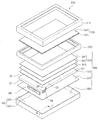
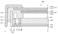
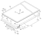
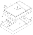
図1は、本発明の一実施形態による表示装置の分解斜視図であり、図2Aは図1のI−I’線に沿って切断された面を示す断面図であり、図2Bは図1に示した発光ユニット、導光板、反射部材、及び表示パネルの結合状態を示す分解斜視図である。 FIG. 1 is an exploded perspective view of a display device according to an embodiment of the present invention, FIG. 2A is a cross-sectional view showing a surface cut along line II ′ of FIG. 1, and FIG. It is a disassembled perspective view which shows the coupling | bonding state of the light emitting unit, the light guide plate, reflection member, and display panel which were shown in.
図1、図2A、及び図2Bを参照すると、表示装置600は、バックライトアセンブリ500及び表示パネル520を含む。
バックライトアセンブリ500は光を発生、出射し、表示パネル520はバックライトアセンブリ500からの光を受けて表示領域DAに画像を表示する。
Referring to FIGS. 1, 2A, and 2B, the
The
本実施形態では、表示パネル520は液晶表示パネルであり、この場合に、表示パネル520は複数の画素電極を有する第1基板521、複数の画素電極と対向する共通電極を有する第2基板522、及び第1基板521と第2基板522との間に介在する液晶層(図示せず)を包含する。
しかし、本発明は表示パネル520の種類に限定されることではない。例えば、表示パネル520は、エレクトロ・ウェッティング表示パネル(Electrowetting display panel)及びナノクリスタル表示パネル(nano−crystal display panel)のように、自身では光を発生しない他の種類の表示パネルであることもあり得る。
In this embodiment, the
However, the present invention is not limited to the type of
バックライトアセンブリ500は、発光ユニット100、収納容器580、反射板570、導光板550、モールドフレーム530、複数のシート540、及びカバー部材510を含む。
The
発光ユニット100は、光を発生する。
本実施形態では、発光ユニット100は、印刷回路基板PB及び印刷回路基板PB上に実装されて光を発生する複数の発光ダイオードLGを包含する。
印刷回路基板PBは、導光板550の第1面S1に沿って延長され、これによって、複数の発光ダイオードLGから発生された光は第1面S1を通じて導光板550側へ入射される。
The
In the present embodiment, the
The printed circuit board PB is extended along the first surface S1 of the
本実施形態では、印刷回路基板PBは、導光板550(の出射面)に対して垂直に配置され得る。
しかし、この実施形態と異なりに、図8Aに示すように、印刷回路基板PBは導光板550(の出射面)に対して水平に配置できることもあり得る。
In the present embodiment, the printed circuit board PB may be disposed perpendicular to the light guide plate 550 (the exit surface thereof).
However, unlike this embodiment, as shown in FIG. 8A, the printed circuit board PB may be arranged horizontally with respect to the light guide plate 550 (the exit surface thereof).
収納容器580は、底部585及び底部585から延長される複数の側壁581を具備して、バックライトアセンブリ500の構成要素を収納する。
上述したように、印刷回路基板PBが導光板550の第1面S1と隣接するように配置される場合に、発光ユニット100は複数の側壁581の中で第1面S1と対向する側壁と第1面S1との間に配置され得る。
The
As described above, when the printed circuit board PB is disposed so as to be adjacent to the first surface S1 of the
導光板550は、発光ユニット100で発生した光を受けて光を表示パネル520側へガイドする。
より詳細には、発光ユニット100で発生した光は、第1面S1を通じて導光板550の内部へ入射され、導光板550の内部へ入射された光は出射面ESを通じて導光板550から出射される。
本実施形態では、導光板550は、突出部555を包含し、突出部555は導光板550の一側面から突出される。
The
More specifically, the light generated in the
In the present embodiment, the
導光板550は、第1面S1及び出射面ESの以外に、第1面と対向する第2面S2、第3面S3、及び第1面S1と傾斜する傾斜面SSを有する連結面LSを包含する。
本実施形態では、第1〜第3面(S1、S2、S3)及び連結面LSは導光板550の側面であり、この場合に、傾斜面SSは突出部555が有する表面の中のいずれか1つである。
連結面LSは、第1面S1と第2面S2との間に順次的に配列されて第1面S1と第2面S2を連結し、第3面S3は連結面LSと対向する。
In addition to the first surface S1 and the emission surface ES, the
In the present embodiment, the first to third surfaces (S1, S2, S3) and the connection surface LS are side surfaces of the
The connection surface LS is sequentially arranged between the first surface S1 and the second surface S2 to connect the first surface S1 and the second surface S2, and the third surface S3 faces the connection surface LS.
本実施形態では、連結面LSは第1連結面LS1、傾斜面SS、及び第2連結面LS2を包含し、第1連結面LS1、傾斜面SS、及び第2連結面LS2は第1面S1と第2面S2との間に順次的に配列される。即ち、連結面LSの中で第1連結面LS1は第1面S1と連結され、第2連結面LS2は第2面S2に連結され、傾斜面SSは第1連結面LS1と第2連結面LS2とを連結する。 In the present embodiment, the connecting surface LS includes the first connecting surface LS1, the inclined surface SS, and the second connecting surface LS2, and the first connecting surface LS1, the inclined surface SS, and the second connecting surface LS2 are the first surface S1. And the second surface S2. That is, among the connection surfaces LS, the first connection surface LS1 is connected to the first surface S1, the second connection surface LS2 is connected to the second surface S2, and the inclined surface SS is connected to the first connection surface LS1 and the second connection surface. Connect LS2.
本実施形態では、平面上から見て第1面S1及び第2面S2の各々は第1方向D1に並行し、平面上から見て第1及び第2連結面LS1、LS2の各々は第1方向D1と実質的に直交する第2方向D2に並行する。
また、平面上から見て傾斜面SSは、第1及び第2方向D1、D2と異なる第3方向D3と並行し、平面上から見て突出部555及び突出部555が有する傾斜面SSは表示領域DAと離隔している。
In the present embodiment, each of the first surface S1 and the second surface S2 is parallel to the first direction D1 when viewed from above, and each of the first and second coupling surfaces LS1 and LS2 is the first when viewed from above. Parallel to the second direction D2 substantially orthogonal to the direction D1.
In addition, the inclined surface SS when viewed from above is parallel to the third direction D3 different from the first and second directions D1 and D2, and the inclined surface SS that the protruding
また、平面上から見て第1面S1は、傾斜面SSと鋭角を形成し、この鋭角は第1面S1から傾斜面SSまで右回りに回転して定義され得る。
また、本実施形態では、複数の発光ダイオードLGは、第1面S1に沿って配列され、平面上から見て複数の発光ダイオードLGの中で最初に配置された発光ダイオードと最後に配置された発光ダイオードとの間の距離を第1離隔距離LT2と定義し、平面上から見て第1面S1の長さを第1長さLT1と定義すれば、第1離隔距離LT2は第1長さLT1より小さい。
Further, when viewed from above, the first surface S1 forms an acute angle with the inclined surface SS, and this acute angle can be defined by rotating clockwise from the first surface S1 to the inclined surface SS.
In the present embodiment, the plurality of light emitting diodes LG are arranged along the first surface S1, and are disposed first and last among the plurality of light emitting diodes LG as viewed from above. If the distance from the light emitting diode is defined as the first separation distance LT2, and the length of the first surface S1 is defined as the first length LT1 when viewed from above, the first separation distance LT2 is the first length. Less than LT1.
また、印刷回路基板PBは、大略的に第1離隔距離LT2に対応する長さを有することができるので、印刷回路基板PBの長さは第1長さLT1より小さい。
したがって、印刷回路基板PBが高価なメタルコア印刷回路基板(metal core printed circuit board、MCPCB)である場合に、印刷回路基板PBが第1長さLT1に対応する長さを有する必要がないので、印刷回路基板PBの製造単価を減少させることができ、印刷回路基板PB上に配置される発光ダイオードLGの個数を減少されることができる。
In addition, since the printed circuit board PB can have a length corresponding to the first separation distance LT2, the length of the printed circuit board PB is smaller than the first length LT1.
Therefore, when the printed circuit board PB is an expensive metal core printed circuit board (MCPCB), the printed circuit board PB does not need to have a length corresponding to the first length LT1. The manufacturing cost of the circuit board PB can be reduced, and the number of light emitting diodes LG disposed on the printed circuit board PB can be reduced.
反射部材RMは、突出部555の表面上に配置され、より詳細には、反射部材RMは、傾斜面SS上に配置される。
したがって、発光ユニット100から発生して第1面S1及び傾斜面SSを順次に透過した光は反射部材RMで反射されて導光板550のコーナー部(第1面S1と第3面S3でなす)及びコーナー部の周辺へ提供される。
したがって、傾斜面SS上に反射部材RMを配置することによって、導光板550のコーナー部及びコーナー部の周辺へ提供される光量と導光板550の残る部分へ提供される光量の差を減少させることができる。これについては、図3を参照してより詳細に説明される。
The reflecting member RM is disposed on the surface of the protruding
Therefore, the light generated from the
Therefore, by disposing the reflecting member RM on the inclined surface SS, the difference between the light amount provided to the corner portion of the
本発明の実施形態では、反射部材RMは、第1面S1と傾斜面SSを連結する第1連結面LS1上にさらに配置することもできる。
また、本発明の実施形態では、反射部材RMは反射テープであり得る。
反射テープは、その表面がミラーのような機能を有するように、表面は銀Ag及びアルミニウムのような反射物質でコーティングされるか、或いは表面は白色のポリエチレンテレフタレート(polyethylene terephthalate、PET)、及びポリカーボネート(poly carbonate、PC)のような光を反射させる物質でコーティングされ得る。
In the embodiment of the present invention, the reflecting member RM may be further disposed on the first connecting surface LS1 that connects the first surface S1 and the inclined surface SS.
In the embodiment of the present invention, the reflection member RM may be a reflection tape.
The reflective tape is coated with a reflective material such as silver Ag and aluminum so that the surface functions as a mirror, or the surface is white polyethylene terephthalate (PET) and polycarbonate. It can be coated with a material that reflects light, such as (poly carbonate, PC).
また、本発明の他の実施形態では、反射部材RMは、傾斜面SS上に配置された反射層であることもあり得る。
この場合に、反射層は、アルミニウムのように光反射度が優れた物質が傾斜面SS上に蒸着されて形成されるか、或いは傾斜面SS上に白色のアクリル系列の物質が塗布されて形成され得る。
In another embodiment of the present invention, the reflection member RM may be a reflection layer disposed on the inclined surface SS.
In this case, the reflective layer is formed by depositing a material having excellent light reflectivity such as aluminum on the inclined surface SS, or by applying a white acrylic material on the inclined surface SS. Can be done.
反射板570は、ポリエチレンテレフタレート(polyethylene terephthalate、PET)及びアルミニウムのような光を反射する物質を含んで収納容器580の底部585と導光板550との間に配置される。
したがって、発光ユニット100から発生して導光板550側へ入射されなかった光は反射板570によって反射された後、導光板550へ入射され得る。
The
Therefore, the light generated from the
モールドフレーム530は、収納容器580に結合されて導光板550の縁を収納容器580の底部585に支持する。
モールドフレーム530の一部分は、底部585と平行な方向に延長されて複数のシート540及び表示パネル520がモールドフレーム530上に安着され得る。
The
A part of the
複数のシート540は、表示パネル520と導光板550との間に配置される。
複数のシート540は、導光板550から出射されて表示パネル520側へ入射される光の経路を調節する光学シートを包含する。
本発明の実施形態では、複数のシート540は各々が導光板550から出射された光を拡散させる上部拡散シート541、下部拡散シート543、及び導光板550から出射された光を集光するプリズムシート542を包含することができる。
The plurality of
The plurality of
In the embodiment of the present invention, each of the plurality of
カバー部材510は、表示パネル520の表示領域DAが露出されるようにその一部が開口され、表示パネル520の枠をカバーして収納容器580と結合される。
カバー部材510が、収納容器580と締結されることによって、収納容器580が有する収納空間内にバックライトアセンブリ500の構成要素が安定的に収納され得る。
The
By fastening the
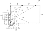
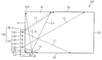
図3は、図2Bに示した導光板側へ入射された光の分布を示す平面図である。
図3を参照すると、発光ユニット100は、印刷回路基板PB及び印刷回路基板PB上に実装された複数の発光ダイオードLGを含む。
複数の発光ダイオードLGは、導光板550の第1面S1に沿って配列されて、複数の発光ダイオードLGから発生された光は第1面S1を通じて導光板550側へ入射される。
FIG. 3 is a plan view showing the distribution of light incident on the light guide plate side shown in FIG. 2B.
Referring to FIG. 3, the
The plurality of light emitting diodes LG are arranged along the first surface S1 of the
本実施形態で、複数の発光ダイオードLGの個数を6つであると仮定し、6つの発光ダイオードLGの中で最初に配置された発光ダイオードから最後に配置された発光ダイオードを順次に第1〜第6発光ダイオード(LG1、LG2、LG3、LG4、LG5、LG6)であると定義する。
本実施形態で、第1〜第6発光ダイオード(LG1、LG2、LG3、LG4、LG5、LG6)の各々から出射された光が放射される角度は互いに同一であり、放射される角度は平面上から見て約100°〜約150°であり得る。
In the present embodiment, it is assumed that the number of the plurality of light emitting diodes LG is six, and among the six light emitting diodes LG, the light emitting diodes arranged first to the light emitting diodes arranged first to first are sequentially arranged. It is defined as the sixth light emitting diode (LG1, LG2, LG3, LG4, LG5, LG6).
In the present embodiment, the angles at which the light emitted from each of the first to sixth light emitting diodes (LG1, LG2, LG3, LG4, LG5, LG6) is emitted are the same, and the emitted angles are on a plane. Viewed from about 100 ° to about 150 °.
例えば、第1発光ダイオードLG1から発生される第1光L1が放射される第1放射角度G1及び第5発光ダイオードLG5から発生される第2光L2が放射される第2放射角度G2の各々の大きさは約100°〜約150°であり、より詳細には、約120°であり得る。
したがって、第1及び第5発光ダイオードLG1、LG5の間に位置した第2〜第4発光ダイオード(LG2、LG3、LG4)から発生される光が導光板550内に放射される範囲は、第1及び第5発光ダイオードLG1、LG5から発生される光が導光板550内に放射される範囲の間に位置することができる。
For example, each of the first radiation angle G1 at which the first light L1 generated from the first light emitting diode LG1 is emitted and the second radiation angle G2 at which the second light L2 generated from the fifth light emitting diode LG5 is emitted. The magnitude is from about 100 ° to about 150 °, and more specifically can be about 120 °.
Accordingly, the range in which light generated from the second to fourth light emitting diodes (LG2, LG3, LG4) positioned between the first and fifth light emitting diodes LG1, LG5 is radiated into the
また、発光ダイオードLGの中で導光板550の突出部555に最も隣接する第6発光ダイオードLG6は、突出部555を介して反射部材RMと対向する。
したがって、第6発光ダイオードLG6から発生した第3光L3は、第1面S1及び傾斜面SSを順次に通過した後、反射部材RMによって反射されて導光板550の第1コーナー部CP1及び第1コーナー部CP1の周辺側へ進行する。
第1コーナー部CP1及び第1コーナー部CP1の周辺を第1部分A1として定義すれば、上述した経路にしたがって進行する第3光L3によって第1部分A1側へ提供される光量を増加させることができる。導光板550で第1コーナー部CP1は第1面S1と第3面S3が会う部分として定義される。
In addition, the sixth light emitting diode LG6 that is closest to the protruding
Accordingly, the third light L3 generated from the sixth light emitting diode LG6 sequentially passes through the first surface S1 and the inclined surface SS, and then is reflected by the reflecting member RM to be reflected by the first corner portion CP1 and the first corner of the
If the first corner portion CP1 and the periphery of the first corner portion CP1 are defined as the first portion A1, the amount of light provided to the first portion A1 side by the third light L3 traveling along the above-described path can be increased. it can. In the
一方、本実施形態と異なりに、発光ユニット100が第1〜第5発光ダイオード(LG1、LG2、LG3、LG4、LG5)のみで構成された場合に、第1〜第5発光ダイオード(LG1、LG2、LG3、LG4、LG5)から発生した光が導光板550内に放射される範囲を考慮すると、導光板550の第1部分A1側へ提供される第1光量は第1部分A1を除外した導光板550の残る部分側へ提供される第2光量より少ないことがあり得る。
しかし、本実施形態では、発光ユニット100は、第6発光ダイオードLG6、傾斜面SSを有する突出部555及び反射部材RMを包含するので、先に上述した経路にしたがって進行する第3光L3によって第1光量を補充することができるので、第1光量と第2光量の差が最小化になり得る。
On the other hand, unlike the present embodiment, when the
However, in the present embodiment, since the
また、本実施形態と異なりに、発光ユニット100が第1〜第5発光ダイオード(LG1、LG2、LG3、LG4、LG5)のみで構成された場合に、第1〜第5発光ダイオード(LG1、LG2、LG3、LG4、LG5)から発生した光が導光板550内に放射される範囲を考慮すると、導光板550の第2コーナー部CP2及び第2コーナー部CP2の周辺で定義される第2部分A2へ提供される第3光量は第1光量より少ないことがあり得る。
しかし、本実施形態では、発光ユニット100は第6発光ダイオードLG6、傾斜面SSを有する突出部555及び反射部材RMを含み、第6発光ダイオードLG6から発生した第3光L3は、約100°〜約150°に放射されて反射部材RMで反射されるので、反射した第3光L3の一部が第2部分A2側へ提供されて第3光量が補充され得る。
Further, unlike the present embodiment, when the
However, in the present embodiment, the
上述した内容を総合すれば、本実施形態では、導光板550の第1及び第2部分A1、A2へ提供される光量及び第1及び第2部分A1、A2を除外した導光板55の他の部分へ提供される光量の差を最少化することができるので、これによって、導光板550の全体領域に掛けて出力される光の光量が均一になり得る。
In summary, in the present embodiment, the amount of light provided to the first and second portions A1 and A2 of the
図4は、本発明の他の実施形態による導光板及び発光ユニットを示す平面図である。
図4では光を出力する発光ユニット101及び光が入射される導光板550を示し、発光ユニット101は、図1に示した表示装置(図1の符号600)の発光ユニット(図1の符号100)を代替することができる。
したがって、図4を説明することにおいて、先に説明した構成要素に対しては図面符号を併記し、構成要素に対する重複した説明は省略する。
FIG. 4 is a plan view illustrating a light guide plate and a light emitting unit according to another embodiment of the present invention.
4 shows a
Therefore, in the description of FIG. 4, the constituent elements described above are denoted by the same reference numerals, and redundant description of the constituent elements is omitted.
図4を参照すれば、発光ユニット101は、印刷回路基板PB_1及び印刷回路基板PB_1に実装される複数の発光ダイオードLGを含む。
本実施形態では、平面上から見て複数の発光ダイオードLGは、導光板550の第1面S1の一側から他側まで順次に配列される。
仮に、本実施形態と異なり、発光ユニット101が第1〜第5発光ダイオード(LG1、LG2、LG3、LG4、LG5)のみで構成される場合に、第1〜第5発光ダイオード(LG1、LG2、LG3、LG4、LG5)の各々から発生する光は、約100°〜約150°の放射角度で導光板550内へ提供される。
Referring to FIG. 4, the
In the present embodiment, the plurality of light emitting diodes LG as viewed from above are sequentially arranged from one side of the first surface S1 of the
Unlike the present embodiment, when the
この場合に、導光板550で第1部分P1及び第3部分P3のように第1〜第5発光ダイオード(LG1、LG2、LG3、LG4、LG5)の各々の位置に対応する部分の各々へ提供される光量を第1光量であると定義し、第2部分P2及び第4部分P4のように第1〜第5発光ダイオード(LG1、LG2、LG3、LG4、LG5)の中で互いに隣接する2つの間に対応する部分の各々へ提供される光量を第2光量であると定義すれば、第2光量は第1光量より小さいことがあり得る。
しかし、本実施形態では、発光ユニット101は傾斜面SSと対向する第6発光ダイオードLG6を含み、これによって、第6発光ダイオードLG6から発生して反射部材RMで反射される第3光L3を利用して第2光量を補充することができるので、第1光量と第2光量との間の差が最小化になり得る。
In this case, the
However, in the present embodiment, the
また、第3光L3によって第2光量のみならず、第1光量も増加することができるが、第1及び第3部分P1、P3で発光ユニット101から発生した光は第1面S1を入射する時、第1面S1で散乱され、これによって第1及び第3部分P1、P3は輝度が大きく減少させられる。
したがって、第3光L3によって第1及び第2光量が補充されても、第3光L3によって第1光量が補充される効果より第2光量が補充される効果が大きいので、全般的に第3光L3によって導光板550の全体領域に掛けて出力される輝度が均一になる効果が発生され得る。
The third light L3 can increase not only the second light amount but also the first light amount, but the light generated from the
Accordingly, even if the first and second light amounts are supplemented by the third light L3, the effect of supplementing the second light amount is greater than the effect of supplementing the first light amount by the third light L3. The light L3 may produce an effect of uniforming the luminance output over the entire area of the
さらに、図3及び図4に示した実施形態を比較する時、図4に示した実施形態では第2及び第4部分P2、P4へ提供される第3光L3の光量が増加されるように傾斜面SSと第1面S1とが形成する角度AGが図3に示した実施形態の場合に比べて小さくなり得る。 Further, when comparing the embodiment shown in FIGS. 3 and 4, the light quantity of the third light L3 provided to the second and fourth portions P2 and P4 is increased in the embodiment shown in FIG. The angle AG formed by the inclined surface SS and the first surface S1 can be smaller than that in the embodiment shown in FIG.
図5は、本発明のさらに他の実施形態による導光板及び発光ユニットを示す平面図である。
図5では光を出力する発光ユニット102及び光が入射される導光板551を示し、光ユニット102は図1に示した表示装置(図1の符号600)の発光ユニット(図1の符号100)を代替することができ、導光板551は図1に示した導光板(図1の符号550)を代替することができる。
図5を説明することにおいて、先に説明した構成要素に対しては図面符号を併記し、構成要素に対する重複した説明は省略する。
FIG. 5 is a plan view illustrating a light guide plate and a light emitting unit according to still another embodiment of the present invention.
5 shows a
In the description of FIG. 5, the constituent elements described above are denoted by the same reference numerals, and redundant description of the constituent elements is omitted.
図5を参照すると、発光ユニット102は、印刷回路基板PB_2及び印刷回路基板PB_2に実装される複数の発光ダイオードLGを含む。
図1に示した実施形態では光が入射される第1面(図1の符号S1)は導光板(図1の符号500)を定義する短辺の中のいずれか1つであると定義したが、図5に示す実施形態では光が入射される第1面S1は導光板551を定義する長辺の中のいずれか1つであると定義する。
Referring to FIG. 5, the
In the embodiment shown in FIG. 1, the first surface on which light is incident (reference numeral S1 in FIG. 1) is defined as one of the short sides defining the light guide plate (
本実施形態でも前述の実施形態と同様に、複数の発光ダイオードLGの中で突出部555に最も隣接する第6発光ダイオードLG6は傾斜面SSに対向するように配置され、これによって、第6発光ダイオードLG6から発生した第3光L3は、第1面S1及び傾斜面SSを順次に透過した以後に反射部材RMで反射されて導光板551の第1及び第2部分A1、A2側へ提供される。
したがって、導光板551の全体に掛けて均一な光量が提供でき、これによって、導光板551は全体領域に掛けて出力される光の輝度が均一になり得る。
Also in the present embodiment, the sixth light emitting diode LG6 closest to the protruding
Accordingly, a uniform amount of light can be provided over the entire
図6Aは、本発明の他の実施形態による表示装置の断面図であり、図6Bは、図6Aに示す発光ユニット、導光板、反射部材、及び表示パネルの結合状態を示す分解斜視図である。
図6A及び図6Bに示す表示装置601は、図1及び図2Aに示した表示装置600に比べて構成要素として離隔部材STを構成要素としてさらに含む。
したがって、図6A及び図6Bを説明することにおいて、先に図1、図2A、図2B及び図3を参照して説明した構成要素に対しては図面符号を併記し、構成要素に対する重複した説明は省略する。
6A is a cross-sectional view of a display device according to another embodiment of the present invention, and FIG. 6B is an exploded perspective view illustrating a combined state of the light emitting unit, the light guide plate, the reflecting member, and the display panel shown in FIG. 6A. .
The
Therefore, in describing FIGS. 6A and 6B, the constituent elements described above with reference to FIGS. 1, 2A, 2B, and 3 are denoted by the same reference numerals, and redundant descriptions of the constituent elements are provided. Is omitted.
図6A及び図6Bを参照すると、本実施形態で表示装置601は、離隔部材STをさらに含む。
離隔部材STは、発光ユニット100と導光板550との間に配置されて発光ユニット100と導光板550との間の間隔を維持する。また、離隔部材STには複数の発光ダイオードLGの位置に対応して貫通ホールHLが形成され、これによって、複数の発光ダイオードLGから発生する光は貫通ホールHL及び第1面S1を通じて導光板550側へ入射され得る。
本実施形態で、離隔部材STは、シリコンのような絶縁性物質含むことができる。したがって、印刷回路基板PBから発生する熱は導光板550側へ直接的に伝達されないので、熱によって導光板550の形状が変形することが防止され得る。
Referring to FIGS. 6A and 6B, in the present embodiment, the
The separation member ST is disposed between the
In the present embodiment, the separation member ST may include an insulating material such as silicon. Therefore, since the heat generated from the printed circuit board PB is not directly transmitted to the
図7Aは、本発明のさらに他の実施形態による表示装置の断面図であり、図7Bは図7Aに示す発光ユニット、導光板、反射部材、表示パネル、及び収納容器の結合状態を示す分解斜視図である。
図7A及び図7Bに示す表示装置602は、図1及び図2Aに示した表示装置600に比べて構成要素として離隔部材586を構成要素としてさらに含む。
したがって、図7A及び図7Bを説明することにおいて、先に図1、図2A、図2B及び図3を参照して説明した構成要素に対しては図面符号を併記し、構成要素に対しては重複した説明は省略する。
7A is a cross-sectional view of a display device according to still another embodiment of the present invention, and FIG. 7B is an exploded perspective view showing a combined state of the light emitting unit, the light guide plate, the reflecting member, the display panel, and the storage container shown in FIG. 7A. FIG.
The
Accordingly, in describing FIGS. 7A and 7B, the components described above with reference to FIGS. 1, 2A, 2B, and 3 are denoted by the same reference numerals, and the components are not described. A duplicate description is omitted.
図7A及び図7Bを参照すると、本実施形態で表示装置602は、離隔部材586を含む。
離隔部材586は、発光ユニット100と導光板550との間に配置されて発光ユニット100と導光板550との間の間隔を維持させる。また、離隔部材550には複数の発光ダイオードLGの位置に対応して貫通ホールHL_1が形成され、これによって、複数の発光ダイオードLGから発生する光は貫通ホールHL_1及び第1面S1を通じて導光板550側へ入射される。
Referring to FIGS. 7A and 7B, the
The
本実施形態で、離隔部材586は、収納容器580の底部585から延長されて収納容器580の側壁581と水平であり得る。
したがって、印刷回路基板PBから発生する熱は、導光板550側へ直接伝達されなく、熱は離隔部材586側へ伝達されて収納容器580を通じて外部へ容易に放出することができ、これによって、熱によって導光板550の形状が変形することが防止され得る。
In this embodiment, the
Therefore, the heat generated from the printed circuit board PB is not directly transmitted to the
図8Aは、本発明のさらに他の実施形態による発光ユニット、導光板、及び表示パネルの結合状態を示す分解斜視図であり、図8Bは図8Aに示す導光板側へ入射された光の分布を示す平面図である。
図8A及び図8Bに示す実施形態によるバックライトアセンブリは、導光板552及び発光ユニット103を除外すれば、図1に示したバックライトアセンブリ(図1の符号500)と同一な構成を有する。
したがって、図8A及び図8Bを説明することにおいて、導光板552及び発光ユニット103の構造に対して主に説明し、残る構成要素に対しては図面符号を併記し、構成要素に対しては重複した説明は省略する。
8A is an exploded perspective view illustrating a combined state of a light emitting unit, a light guide plate, and a display panel according to still another embodiment of the present invention, and FIG. 8B is a distribution of light incident on the light guide plate side illustrated in FIG. 8A. FIG.
The backlight assembly according to the embodiment shown in FIGS. 8A and 8B has the same configuration as the backlight assembly shown in FIG. 1 (
Therefore, in describing FIG. 8A and FIG. 8B, the structure of the
図8A及び図8Bを参照すると、発光ユニット103は、印刷回路基板PB_3及び印刷回路基板PB_3上に配置された複数の発光ダイオードLGを含む。
本実施形態では、印刷回路基板PB_3は導光板552と水平に配置され、複数の発光ダイオードLGは導光板552の入射面と対向するよう配置される。
これによって、印刷回路基板PB_3は、導光板552と収納容器580の底部585との間に配置される。
Referring to FIGS. 8A and 8B, the
In the present embodiment, the printed circuit board PB_3 is disposed horizontally with the
Accordingly, the printed circuit board PB_3 is disposed between the
本実施形態では、印刷回路基板PB_3は、導光板552の第1コーナー部CP1と重畳する。
導光板552が第1面S1、第1面S1と対向する第2面S2、第3面S3、及び第3面S3と対向する第4面S4を有し、第1コーナー部CP1は第1面S1と第4面S4が会って定義されるものであり、第2コーナー部CP2は第1面S1と第3面S3が会って定義されるものである。
In the present embodiment, the printed circuit board PB_3 overlaps with the first corner portion CP1 of the
The
本実施形態では、複数の発光ダイオードLGの中で第1面S1と対向する発光ダイオードは複数に提供され、複数の発光ダイオードLGの中で第4面S4と対向する発光ダイオードは単数で提供される。
例えば、複数の発光ダイオードLGが第1〜第6発光ダイオード(LG1、LG2、LG3、LG4、LG5、LG6)を含むと仮定する時、第1〜第5発光ダイオード(LG1、LG2、LG3、LG4、LG5)は第1面S1と対向し、第6発光ダイオードLG6は第4面S4と対向する。この場合、第1面S1は第1方向D1に延長され、第4面S4は第1方向D1と実質的に直交する第2方向D2に延長されるので、第1〜第5発光ダイオード(LG1、LG2、LG3、LG4、LG5)の各々は第6発光ダイオードLG6と実質的に直交して配置される。
In the present embodiment, a plurality of light emitting diodes facing the first surface S1 are provided among the plurality of light emitting diodes LG, and a single light emitting diode facing the fourth surface S4 is provided among the plurality of light emitting diodes LG. The
For example, when it is assumed that the plurality of light emitting diodes LG include first to sixth light emitting diodes (LG1, LG2, LG3, LG4, LG5, LG6), the first to fifth light emitting diodes (LG1, LG2, LG3, LG4). LG5) is opposed to the first surface S1, and the sixth light emitting diode LG6 is opposed to the fourth surface S4. In this case, the first surface S1 is extended in the first direction D1, and the fourth surface S4 is extended in the second direction D2 substantially orthogonal to the first direction D1, so that the first to fifth light emitting diodes (LG1) , LG2, LG3, LG4, LG5) are arranged substantially orthogonal to the sixth light emitting diode LG6.
上述した導光板552及び発光ユニット103の構造によれば、第6発光ダイオードLG6から発生した第3光L3は第4面S4を通過した後、導光板550の第2コーナー部CP2及び第2コーナー部CP2の周辺側へ進行する。
第2コーナー部CP2及び第2コーナー部CP2の周辺を第1部分A1として定義すれば、上述した経路にしたがって進行する第3光L3によって第1部分A1側へ提供される第1光量が増加する。これによって、第1光量と第1部分A1を除外した導光板550の残る部分に提供される光量との差が減少される。
また、第6発光ダイオードLG6から提供される第3光L3の放射範囲は、第1コーナー部CP1及び第1コーナー部CP1の周辺で定義される導光板552の第2部分A2をカバーすることができるので、第2部分A2側に提供される光量が補充され得る。
According to the structure of the
If the second corner portion CP2 and the periphery of the second corner portion CP2 are defined as the first portion A1, the first light amount provided to the first portion A1 side by the third light L3 traveling along the above-described path increases. . Accordingly, the difference between the first light amount and the light amount provided to the remaining portion of the
Further, the radiation range of the third light L3 provided from the sixth light emitting diode LG6 may cover the first corner portion CP1 and the second portion A2 of the
尚、本発明は、上述の実施形態に限られるものではない。本発明の技術的範囲から逸脱しない範囲内で多様に変更実施することが可能である。 The present invention is not limited to the embodiment described above. Various modifications can be made without departing from the technical scope of the present invention.
100 発光ユニット
500 バックライトアセンブリ
510 カバー部材
520 表示パネル
521 第1基板
522 第2基板
530 モールドフレーム
540 複数のシート
541 上部拡散シート
542 プリズムシート
543 下部拡散シート
550 導光板
555 突出部
570 反射板
580 収納容器
600 表示装置
RM 反射部材
PB 印刷回路基板
LG 発光ダイオード
SS 傾斜面
LS 連結面
DESCRIPTION OF
Claims (14)
前記光を受けて画像を表示する表示パネルとを有し、
前記バックライトアセンブリは、前記光を発生させる発光ユニットと、
前記発光ユニットから提供された光を前記表示パネル側へガイドし、側面から突出した突出部を含む導光板と、
前記突出部の表面上に配置されて前記発光ユニットから前記突出部側へ提供された光を前記導光板のコーナー部及び前記コーナー部の周辺に向けて反射させる反射部材とを含むことを特徴とする表示装置。 A backlight assembly that generates and emits light;
A display panel that receives the light and displays an image;
The backlight assembly includes a light emitting unit that generates the light;
A light guide plate that guides the light provided from the light emitting unit to the display panel and includes a protruding portion protruding from a side surface;
A reflection member disposed on the surface of the protrusion and reflecting light provided from the light emitting unit toward the protrusion toward the corner of the light guide plate and the periphery of the corner. Display device.
前記傾斜面は、前記突出部の表面の中のいずれか1つであることを特徴とする請求項1に記載の表示装置。 The light guide plate includes a first surface on which the light provided from the light emitting unit is incident, an exit surface from which the incident light is emitted, a second surface facing the first surface, and the first surface. A connecting surface for connecting the first surface to the second surface having an inclined surface inclined with respect to the surface;
The display device according to claim 1, wherein the inclined surface is any one of surfaces of the protrusions.
前記印刷回路基板上に前記第1面に沿って配列されて前記光を発生する複数の発光ダイオードとを含むことを特徴とする請求項2に記載の表示装置。 The light emitting unit includes a printed circuit board extended along the first surface;
The display device according to claim 2, further comprising a plurality of light emitting diodes arranged on the printed circuit board along the first surface to generate the light.
平面上から見て、前記突出部は前記表示領域から離隔するよう突出していることを特徴とする請求項1に記載の表示装置。 The display panel includes a display area,
The display device according to claim 1, wherein the protruding portion protrudes away from the display area when viewed from above.
前記光を受けて画像を表示する表示パネルとを有し、
前記バックライトアセンブリは、前記光を発生する発光ユニットと、
前記発光ユニットから提供された光を前記表示パネル側へガイドする導光板とを含み、
前記発光ユニットは、前記導光板と水平に配置されて平面上から見て前記導光板の第1コーナー部と重畳される印刷回路基板と、
前記印刷回路基板上に配置され、前記第1コーナー部を定義する2つの側面を通じて前記導光板側に光を提供する複数の発光ダイオードとを含むことを特徴とする表示装置。 A backlight assembly that generates and emits light;
A display panel that receives the light and displays an image;
The backlight assembly includes a light emitting unit that generates the light;
A light guide plate that guides light provided from the light emitting unit to the display panel side,
The light-emitting unit is disposed horizontally with the light guide plate, and is superimposed on the first corner portion of the light guide plate when viewed from above,
A display device comprising: a plurality of light emitting diodes disposed on the printed circuit board and providing light to the light guide plate side through two side surfaces defining the first corner portion.
前記印刷回路基板は、前記導光板と前記底部との間に位置することを特徴とする請求項9に記載の表示装置。
A storage container for storing the light guide plate and the light emitting unit with a bottom and a side wall extending from the bottom;
The display device according to claim 9, wherein the printed circuit board is located between the light guide plate and the bottom portion.
Applications Claiming Priority (2)
| Application Number | Priority Date | Filing Date | Title |
|---|---|---|---|
| KR10-2013-0007569 | 2013-01-23 | ||
| KR1020130007569A KR20140094914A (en) | 2013-01-23 | 2013-01-23 | Dispaly apparatus having backlight assembly |
Publications (2)
| Publication Number | Publication Date |
|---|---|
| JP2014142590A true JP2014142590A (en) | 2014-08-07 |
| JP2014142590A5 JP2014142590A5 (en) | 2016-11-04 |
Family
ID=51190684
Family Applications (1)
| Application Number | Title | Priority Date | Filing Date |
|---|---|---|---|
| JP2013198265A Withdrawn JP2014142590A (en) | 2013-01-23 | 2013-09-25 | Display device |
Country Status (4)
| Country | Link |
|---|---|
| US (1) | US20140204609A1 (en) |
| JP (1) | JP2014142590A (en) |
| KR (1) | KR20140094914A (en) |
| CN (1) | CN103943041A (en) |
Families Citing this family (3)
| Publication number | Priority date | Publication date | Assignee | Title |
|---|---|---|---|---|
| CN204141394U (en) * | 2014-09-28 | 2015-02-04 | 北京京东方茶谷电子有限公司 | Backlight module and display unit |
| CN111509110A (en) * | 2014-11-18 | 2020-08-07 | 首尔半导体株式会社 | Light emitting device |
| KR102553499B1 (en) | 2016-07-26 | 2023-07-10 | 삼성전자주식회사 | Display apparatus |
Family Cites Families (25)
| Publication number | Priority date | Publication date | Assignee | Title |
|---|---|---|---|---|
| US6295405B1 (en) * | 1997-07-25 | 2001-09-25 | Physical Optics Corporation | Light pipe for a backlighting system |
| KR100783592B1 (en) * | 2002-02-05 | 2007-12-07 | 삼성전자주식회사 | Illuminating apparatus and display device using the same |
| US6871974B2 (en) * | 2003-06-27 | 2005-03-29 | Matsushita Electric Industrial Co., Ltd. | Lighting unit and liquid crystal device using the same |
| JP4007340B2 (en) * | 2003-09-19 | 2007-11-14 | セイコーエプソン株式会社 | Electro-optical device, electronic apparatus, and method of manufacturing electro-optical device |
| US7894012B2 (en) * | 2005-11-28 | 2011-02-22 | Sharp Kabushiki Kaisha | Backlight device and liquid crystal display device using the same |
| CN100529888C (en) * | 2006-12-22 | 2009-08-19 | 群康科技(深圳)有限公司 | Back light module unit and LCD |
| JP4959506B2 (en) * | 2007-10-31 | 2012-06-27 | 株式会社ジャパンディスプレイイースト | Liquid crystal display |
| JP4939446B2 (en) * | 2008-01-15 | 2012-05-23 | シャープ株式会社 | Surface light source and display device |
| EP2237102A4 (en) * | 2008-03-25 | 2010-12-29 | Sharp Kk | Liquid crystal display device |
| CN101726918B (en) * | 2008-10-29 | 2012-04-11 | 纬创资通股份有限公司 | Display device and electronic device with same |
| CN102282413A (en) * | 2009-01-22 | 2011-12-14 | 夏普株式会社 | Backlight unit and liquid crystal display device |
| TWI402571B (en) * | 2009-04-22 | 2013-07-21 | Advanced Optoelectronic Tech | Backlight module with complementary color zone |
| US20100271841A1 (en) * | 2009-04-27 | 2010-10-28 | Led Folio Corporation | LED Lighting With Light Guide Plate Having Side Reflector |
| TWI380096B (en) * | 2009-05-08 | 2012-12-21 | Au Optronics Corp | Backlight unit |
| KR101546741B1 (en) * | 2009-05-13 | 2015-08-25 | 삼성디스플레이 주식회사 | Light emitting module and display apparatus having the same |
| JP5729581B2 (en) * | 2009-11-12 | 2015-06-03 | Nltテクノロジー株式会社 | Surface emitting device |
| TWI405008B (en) * | 2009-12-04 | 2013-08-11 | Au Optronics Corp | Backlight module and display device having the same |
| TWM381089U (en) * | 2009-12-25 | 2010-05-21 | Coretronic Corp | Backlight module |
| JP2013080562A (en) * | 2010-02-10 | 2013-05-02 | Sharp Corp | Backlight device, liquid crystal display, and television receiver |
| US8786803B2 (en) * | 2010-05-13 | 2014-07-22 | Samsung Display Co., Ltd. | Backlight assembly and display apparatus having the same |
| KR101769971B1 (en) * | 2010-10-29 | 2017-08-22 | 삼성디스플레이 주식회사 | Light guide plate and display device having the same |
| KR101784520B1 (en) * | 2011-03-09 | 2017-10-11 | 엘지디스플레이 주식회사 | Back Light Unit and Liquid Crystal Display Device using the same |
| TWI459093B (en) * | 2011-11-18 | 2014-11-01 | Au Optronics Corp | Backlight module and light source module thereof |
| WO2014017347A1 (en) * | 2012-07-24 | 2014-01-30 | シャープ株式会社 | Display device, and television receiver |
| WO2014017346A1 (en) * | 2012-07-24 | 2014-01-30 | シャープ株式会社 | Display device, and television receiver |
-
2013
- 2013-01-23 KR KR1020130007569A patent/KR20140094914A/en not_active Application Discontinuation
- 2013-05-30 US US13/905,348 patent/US20140204609A1/en not_active Abandoned
- 2013-08-12 CN CN201310349688.XA patent/CN103943041A/en active Pending
- 2013-09-25 JP JP2013198265A patent/JP2014142590A/en not_active Withdrawn
Also Published As
| Publication number | Publication date |
|---|---|
| US20140204609A1 (en) | 2014-07-24 |
| CN103943041A (en) | 2014-07-23 |
| KR20140094914A (en) | 2014-07-31 |
Similar Documents
| Publication | Publication Date | Title |
|---|---|---|
| KR102312522B1 (en) | Display device | |
| KR101867044B1 (en) | Backlight unit, display apparatus using the same, and the lighting apparatus including the same | |
| JP6220147B2 (en) | Backlight assembly and display device having the same | |
| JP2006114467A (en) | Illumination unit and liquid crystal display device equipped with the same | |
| KR20130014005A (en) | Backlight unit and display apparatus using the same | |
| WO2013039001A1 (en) | Illumination device, display device, and television receiving device | |
| JP2014142590A (en) | Display device | |
| JP2006133583A (en) | Liquid crystal display device | |
| KR101231728B1 (en) | backlight unit and display apparatus using the same | |
| KR20160059005A (en) | Blacklight Unit and Liquid Crystal Display Device having the same | |
| JP2013149559A (en) | Lighting system, display device, and television receiver | |
| KR101210648B1 (en) | backlight unit and display apparatus using the same | |
| KR20090054841A (en) | Display device | |
| JP2013026211A (en) | Backlight unit and display device using the same | |
| JP2013161527A (en) | Light guide plate, backlight device and liquid crystal display device | |
| US9244213B2 (en) | Edge-light type planar light source device | |
| KR101210649B1 (en) | backlight unit and display apparatus using the same | |
| US9052542B2 (en) | Light source package and backlight unit including the light source package | |
| CN111338129A (en) | Backlight module and display device | |
| KR20090081664A (en) | Light emitting diode backlight unit and liquid crystal display having the same | |
| WO2012053262A1 (en) | Lighting apparatus, and display apparatus provided with same | |
| KR20130020302A (en) | Backlight unit and display apparatus using the same | |
| US20200264479A1 (en) | Lighting device and display device | |
| KR20120134828A (en) | Backlight unit and display apparatus using the same | |
| KR101992362B1 (en) | light unit and illumination system using the same |
Legal Events
| Date | Code | Title | Description |
|---|---|---|---|
| A521 | Request for written amendment filed |
Free format text: JAPANESE INTERMEDIATE CODE: A523 Effective date: 20160914 |
|
| A621 | Written request for application examination |
Free format text: JAPANESE INTERMEDIATE CODE: A621 Effective date: 20160914 |
|
| A761 | Written withdrawal of application |
Free format text: JAPANESE INTERMEDIATE CODE: A761 Effective date: 20170516 |