JP2013026211A - Backlight unit and display device using the same - Google Patents
Backlight unit and display device using the same Download PDFInfo
- Publication number
- JP2013026211A JP2013026211A JP2012029678A JP2012029678A JP2013026211A JP 2013026211 A JP2013026211 A JP 2013026211A JP 2012029678 A JP2012029678 A JP 2012029678A JP 2012029678 A JP2012029678 A JP 2012029678A JP 2013026211 A JP2013026211 A JP 2013026211A
- Authority
- JP
- Japan
- Prior art keywords
- backlight unit
- reflector
- unit according
- reflective
- reflection
- Prior art date
- Legal status (The legal status is an assumption and is not a legal conclusion. Google has not performed a legal analysis and makes no representation as to the accuracy of the status listed.)
- Pending
Links
Images


Classifications
-
- G—PHYSICS
- G02—OPTICS
- G02F—OPTICAL DEVICES OR ARRANGEMENTS FOR THE CONTROL OF LIGHT BY MODIFICATION OF THE OPTICAL PROPERTIES OF THE MEDIA OF THE ELEMENTS INVOLVED THEREIN; NON-LINEAR OPTICS; FREQUENCY-CHANGING OF LIGHT; OPTICAL LOGIC ELEMENTS; OPTICAL ANALOGUE/DIGITAL CONVERTERS
- G02F1/00—Devices or arrangements for the control of the intensity, colour, phase, polarisation or direction of light arriving from an independent light source, e.g. switching, gating or modulating; Non-linear optics
- G02F1/01—Devices or arrangements for the control of the intensity, colour, phase, polarisation or direction of light arriving from an independent light source, e.g. switching, gating or modulating; Non-linear optics for the control of the intensity, phase, polarisation or colour
- G02F1/13—Devices or arrangements for the control of the intensity, colour, phase, polarisation or direction of light arriving from an independent light source, e.g. switching, gating or modulating; Non-linear optics for the control of the intensity, phase, polarisation or colour based on liquid crystals, e.g. single liquid crystal display cells
- G02F1/133—Constructional arrangements; Operation of liquid crystal cells; Circuit arrangements
- G02F1/1333—Constructional arrangements; Manufacturing methods
- G02F1/1335—Structural association of cells with optical devices, e.g. polarisers or reflectors
- G02F1/1336—Illuminating devices
- G02F1/133615—Edge-illuminating devices, i.e. illuminating from the side
-
- G—PHYSICS
- G02—OPTICS
- G02F—OPTICAL DEVICES OR ARRANGEMENTS FOR THE CONTROL OF LIGHT BY MODIFICATION OF THE OPTICAL PROPERTIES OF THE MEDIA OF THE ELEMENTS INVOLVED THEREIN; NON-LINEAR OPTICS; FREQUENCY-CHANGING OF LIGHT; OPTICAL LOGIC ELEMENTS; OPTICAL ANALOGUE/DIGITAL CONVERTERS
- G02F1/00—Devices or arrangements for the control of the intensity, colour, phase, polarisation or direction of light arriving from an independent light source, e.g. switching, gating or modulating; Non-linear optics
- G02F1/01—Devices or arrangements for the control of the intensity, colour, phase, polarisation or direction of light arriving from an independent light source, e.g. switching, gating or modulating; Non-linear optics for the control of the intensity, phase, polarisation or colour
- G02F1/13—Devices or arrangements for the control of the intensity, colour, phase, polarisation or direction of light arriving from an independent light source, e.g. switching, gating or modulating; Non-linear optics for the control of the intensity, phase, polarisation or colour based on liquid crystals, e.g. single liquid crystal display cells
- G02F1/133—Constructional arrangements; Operation of liquid crystal cells; Circuit arrangements
- G02F1/1333—Constructional arrangements; Manufacturing methods
- G02F1/1335—Structural association of cells with optical devices, e.g. polarisers or reflectors
- G02F1/1336—Illuminating devices
- G02F1/133602—Direct backlight
- G02F1/133605—Direct backlight including specially adapted reflectors
Abstract
Description
本発明の実施例は、バックライトユニット及びそれを用いたディスプレイ装置に関する。 Embodiments described herein relate generally to a backlight unit and a display device using the backlight unit.
一般に、代表的な大型ディスプレイ装置としては、LCD(Liquid Crystal Display)、PDP(Plasma Display Panel)などがある。 In general, typical large display devices include LCD (Liquid Crystal Display), PDP (Plasma Display Panel), and the like.
自発光方式のPDPとは異なって、LCDには、自体的な発光素子の不在のため別途のバックライトユニットが必ず必要である。 Unlike the self-light emitting PDP, the LCD always requires a separate backlight unit due to the absence of the light emitting element.
LCDに使用されるバックライトユニットは、光源の位置によってエッジ(edge)方式のバックライトユニットと直下方式のバックライトユニットに区分されるが、エッジ方式では、LCDパネルの左右側面又は上下側面に光源を配置し、導光板を用いて光を全面に均一に分散させるので、光の均一性が良く、パネル厚さの超薄型化が可能である。 The backlight unit used in the LCD is divided into an edge type backlight unit and a direct type backlight unit according to the position of the light source. In the edge type, a light source is provided on the left and right side surfaces or upper and lower side surfaces of the LCD panel. Since the light is uniformly distributed over the entire surface using a light guide plate, the light uniformity is good and the panel thickness can be made ultra-thin.
直下方式は、通常20インチ以上のディスプレイに使用される技術であって、パネルの下部に複数の光源を配置するので、エッジ方式に比べて光効率に優れるという長所を有し、高輝度を要求する大型ディスプレイに主に使用される。 The direct method is a technology that is usually used for displays of 20 inches or more, and has multiple light sources at the bottom of the panel, so it has the advantage of superior light efficiency compared to the edge method and requires high brightness. Mainly used for large displays.
既存のエッジ方式や直下方式のバックライトユニットの光源としては、CCFL(Cold Cathode Fluorescent Lamp)を用いた。 CCFL (Cold Cathode Fluorescent Lamp) was used as the light source of the existing edge type or direct type backlight unit.
しかし、CCFLを用いたバックライトユニットでは、常にCCFLに電源が印加されるので、相当量の電力消耗をもたらし、CRTに比べて約70%水準の色再現率、水銀の添加による環境汚染問題などが短所として指摘されている。 However, in the backlight unit using CCFL, since power is always applied to CCFL, a considerable amount of power is consumed, color reproduction rate of about 70% level compared to CRT, environmental pollution problems due to addition of mercury, etc. Is pointed out as a disadvantage.
前記問題を解消するための代替品として、現在、LED(Light Emitting diode)を用いたバックライトユニットに対する研究が活発に行われている。 As an alternative to solve the above problem, research on a backlight unit using an LED (Light Emitting Diode) is being actively conducted.
LEDをバックライトユニットに使用する場合、LEDアレイの部分的なオン/オフが可能であり、消耗電力を画期的に減少させることができ、RGB LEDの場合、NTSC(National Television System Committee)色再現範囲仕様の100%を上回り、より生々しい画質を消費者に提供することができる。 When the LED is used in the backlight unit, the LED array can be partially turned on / off, and the power consumption can be reduced dramatically. In the case of RGB LED, NTSC (National Television System Committee) color It exceeds 100% of the reproduction range specification and can provide consumers with a more fresh image quality.
本発明の実施例は、導光板なしに反射構造物を用いて、エアガイドを有するバックライトユニット及びそれを用いたディスプレイ装置を提供しようとする。 Embodiments of the present invention provide a backlight unit having an air guide and a display device using the same by using a reflective structure without a light guide plate.
本発明の一実施例は、第1のリフレクタと、一部に傾斜面を有する第2のリフレクタと、第1及び第2のリフレクタの間に配置された少なくとも1つの光源モジュールと、第2のリフレクタに配置された少なくとも1つの反射構造物とを備えることができる。 An embodiment of the present invention includes a first reflector, a second reflector having a partially inclined surface, at least one light source module disposed between the first and second reflectors, and a second reflector And at least one reflective structure disposed on the reflector.
ここで、第2のリフレクタの傾斜面は、第1のリフレクタの表面に対して一定角度だけ傾斜した面であり、傾斜面は、凹面、凸面、平面のうちの少なくとも1つであり得る。 Here, the inclined surface of the second reflector is a surface inclined by a certain angle with respect to the surface of the first reflector, and the inclined surface may be at least one of a concave surface, a convex surface, and a flat surface.
そして、第2のリフレクタの傾斜面は第1のリフレクタと重畳することができる。 The inclined surface of the second reflector can be overlapped with the first reflector.
そして、第2のリフレクタは、少なくとも1つの傾斜面と、少なくとも1つの平面とを有し、第2のリフレクタの平面は第1のリフレクタと平行な面であり、反射構造物は、第2のリフレクタの傾斜面及び平面のうちの少なくとも一面に配置することができる。 The second reflector has at least one inclined surface and at least one plane. The plane of the second reflector is a plane parallel to the first reflector. It can arrange | position to at least 1 surface of the inclined surface and flat surface of a reflector.
また、本発明の一実施例は、第2のリフレクタから一定間隔だけ空間を置いて配置された光学部材をさらに備え、第2のリフレクタと光学部材との間の空間にはエアガイドを形成することができる。 The embodiment of the present invention may further include an optical member disposed at a predetermined interval from the second reflector, and an air guide is formed in the space between the second reflector and the optical member. be able to.
ここで、反射構造物は光学部材から第1の間隔だけ離隔して配置できるが、第1の間隔は第1のリフレクタの厚さより大きくなり得る。 Here, the reflective structure may be spaced apart from the optical member by a first distance, but the first distance may be greater than the thickness of the first reflector.
そして、反射構造物は、第1のリフレクタから水平に延長される水平延長線と第2のリフレクタとの間に位置し得る。 The reflective structure may be positioned between a horizontal extension line extending horizontally from the first reflector and the second reflector.
そして、反射構造物は、光を反射させる反射部と、反射部を支持する支持部とを備えるが、反射部は光源モジュールと同一線上に位置し得る。 And although a reflective structure is provided with the reflection part which reflects light, and the support part which supports a reflection part, a reflection part can be located on the same line as a light source module.
そして、反射部は、光源モジュールと同一方向に配列されるストライプ状又はドット状であり、反射部は複数の突起又は複数の溝を有することができる。 The reflective portion may have a stripe shape or a dot shape arranged in the same direction as the light source module, and the reflective portion may have a plurality of protrusions or a plurality of grooves.
ここで、互いに隣接する複数の突起又は溝は、並んで配列したり、又は交互に配列することができる。 Here, the plurality of adjacent protrusions or grooves can be arranged side by side or alternately.
そして、反射部は、コアと、コアの全体又は一部を取り囲む反射層とを備えることができる。 And a reflection part can be provided with the core and the reflection layer surrounding the whole or a part of core.
ここで、反射層は、同一の反射率を有する1つの反射物質又は互いに異なる反射率を有する複数の反射物質からなることもでき、反射層は、コアの表面から突出したり、又はコアの表面内に挿入することもできる。 Here, the reflective layer may be formed of one reflective material having the same reflectance or a plurality of reflective materials having different reflectances, and the reflective layer may protrude from the surface of the core or be in the surface of the core. Can also be inserted.
そして、支持部は、下部が上部より大きい厚さを有し、支持部の最大幅は、反射部の最大幅と同一であるか、又は反射部の最大幅より大きくなり得る。 In addition, the lower part of the support part has a thickness larger than that of the upper part, and the maximum width of the support part may be the same as or larger than the maximum width of the reflection part.
そして、支持部の最大高さは、反射部の最大高さと同一であるか、又は反射部の最大高さより大きくなり得る。 The maximum height of the support part may be the same as the maximum height of the reflection part or may be larger than the maximum height of the reflection part.
そして、反射部と支持部は結合部材によって結合されるが、結合部材は、支持部の上部面に付着されて反射部の下部面を支持する板状、支持部の上部面に付着されて反射部の周囲を取り囲むリング状、支持部の上部面に付着されて反射部の溝内に挿入される突出形状のうちのいずれか1つであり得る。 The reflection part and the support part are coupled by a coupling member. The coupling member is attached to the upper surface of the support part to support the lower surface of the reflection part, and is attached to the upper surface of the support part and reflected. It may be any one of a ring shape surrounding the periphery of the portion and a protruding shape attached to the upper surface of the support portion and inserted into the groove of the reflection portion.
そして、反射部と支持部は接着剤によって付着することもできる。 And the reflection part and the support part can also adhere with an adhesive agent.
また、反射部と支持部は、1対1の比率で対応して配置したり、又は1対多の比率で対応して配置することができる。 Further, the reflection part and the support part can be arranged in a one-to-one ratio, or can be arranged in a one-to-many ratio.
本発明の一実施例によると、導光板なしに反射構造物を用いて、エアガイドを有するバックライトユニット及びそれを用いたディスプレイ装置を提供することができる。 According to an embodiment of the present invention, it is possible to provide a backlight unit having an air guide and a display device using the same by using a reflective structure without a light guide plate.
以下、各実施例を添付の図面を参照して説明する。 Each embodiment will be described below with reference to the accompanying drawings.
本発明の実施例の説明において、各構成要素の「上又は下」に形成されると記載される場合において、上又は下は、二つの構成要素が互いに直接接触したり、一つ以上の他の構成要素が前記二つの構成要素の間に配置されて形成されることを全て含む。 In the description of the embodiments of the present invention, when it is described as being formed “above or below” each component, the above or below means that two components are in direct contact with each other or one or more other components. All of the components are arranged between the two components.
また、「上又は下」と表現される場合、一つの構成要素を基準にして上側方向のみならず、下側方向の意味も含むことができる。 In addition, the expression “upper or lower” may include not only the upper direction but also the lower direction meaning based on one component.
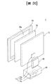
図1A〜図1Cは、本発明の一実施例に係るバックライトユニットを説明するための図であって、図1Aは断面図で、図1Bは平面図で、図1Cは上面斜視図である。 1A to 1C are diagrams for explaining a backlight unit according to an embodiment of the present invention. FIG. 1A is a cross-sectional view, FIG. 1B is a plan view, and FIG. 1C is a top perspective view. .
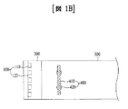
図1A〜図1Cに示すように、バックライトユニットは、少なくとも一つの光源110及び基板120を有する光源モジュール100と、第1のリフレクタ200と、第2のリフレクタ300と、反射部410及び支持部420を有する反射構造物400とを備えることができる。
As shown in FIGS. 1A to 1C, the backlight unit includes a
ここで、光源モジュール100は、第1のリフレクタ200と第2のリフレクタ300との間に位置し、第1のリフレクタ200又は第2のリフレクタ300に隣接するように配置することができる。
Here, the
場合に応じて、光源モジュール100は、第1のリフレクタ200に接触すると同時に第2のリフレクタ300から一定間隔だけ離隔するように配置したり、又は、第2のリフレクタ300に接触すると同時に第1のリフレクタ200から一定間隔だけ離隔するように配置することができる。
Depending on the case, the
また、光源モジュール100は、第1のリフレクタ200と第2のリフレクタ300から一定間隔だけ離隔するように配置したり、又は、第1のリフレクタ200と第2のリフレクタ300に同時に接触することもできる。
Further, the
そして、光源モジュール100は、電極パターンを有する基板120と、光を生成する光源110とを備えることができる。
The
このとき、基板120には、少なくとも1つの光源110を実装することができ、電源を供給するアダプタと光源110を連結するための電極パターンを形成することができる。
At this time, at least one
このような基板120は、ポリエチレンテレフタレート(PET)、ガラス、ポリカーボネート(PC)又はシリコン(Si)などからなり、複数の光源100が実装されるPCB(Printed Circuit Board)基板であり、フィルム状に形成することができる。
Such a
また、基板120としては、単層PCB、多層PCB、セラミック基板、メタルコアPCBなどを選択的に使用することができる。
As the
一方、光源110は、発光ダイオードチップであり、発光ダイオードチップは、ブルーLEDチップ又は紫外線LEDチップで構成したり、又は、レッドLEDチップ、グリーンLEDチップ、ブルーLEDチップ、イエローグリーンLEDチップ及びホワイトLEDチップのうちの少なくとも1つ又はそれ以上を組み合わせたパッケージ形態で構成することもできる。
Meanwhile, the
そして、ホワイトLEDは、ブルーLED上にイエローリン光(Yellow phosphor)を結合したり、ブルーLED上にレッドリン光(Red phosphor)とグリーンリン光(Green phosphor)を同時に使用して具現することができ、ブルーLED上にイエローリン光(Yellow phosphor)、レッドリン光(Red phosphor)及びグリーンリン光(Green phosphor)を同時に使用して具現することもできる。 The white LED may be implemented by combining yellow phosphor on the blue LED or using red phosphor and green phosphor on the blue LED at the same time. In addition, yellow phosphor, red phosphor, and green phosphor may be simultaneously used on a blue LED.
また、光源110は、上面発光型(top view type)発光ダイオードであってもよく、場合に応じては、側面発光型(side view type)発光ダイオードであってもよい。
In addition, the
そして、第1のリフレクタ200と第2のリフレクタ300との間の空間にエアガイドを備えるように、第1のリフレクタ200と第2のリフレクタ300は一定間隔だけ離隔して互いに対向することができる。
Then, the
そして、第1のリフレクタ200は、反射コーティングフィルム及び反射コーティング物質層のうちのいずれか1つで形成され、光源モジュール100から生成された光を第2のリフレクタ300の方向に反射させる役割をすることができる。
The
また、第1のリフレクタ200の表面のうち光源モジュール100と対向する表面上には鋸歯状の反射パターンが形成され、反射パターンの表面は平面又は曲面であり得る。
Further, a sawtooth-like reflection pattern is formed on the surface of the
第1のリフレクタ200の表面に反射パターンを形成する理由は、光源モジュール100で生成された光を第2のリフレクタ300の中央領域に反射させることによって、バックライトユニットの中央領域の輝度を増加させるためである。
The reason for forming the reflection pattern on the surface of the
そして、第2のリフレクタ300は、一部に傾斜面を有することができ、アルミニウム(Al)、銀(Ag)、金(Au)、二酸化チタン(TiO2)などのように高い反射率を有する金属又は金属酸化物を含んで構成することができる。
The
そして、第2のリフレクタ300の傾斜面は、光源モジュール100及び第1のリフレクタ200のうちの少なくとも1つと重畳し得る。
The inclined surface of the
ここで、第2のリフレクタ300の傾斜面は、第1のリフレクタ200の表面に対して一定角度だけ傾斜した面であり、傾斜面は、凹面、凸面及び平面のうちの少なくとも1つであり得る。
Here, the inclined surface of the
場合に応じて、第2のリフレクタ300は、少なくとも1つの傾斜面及び少なくとも1つの平面を有することができるが、第2のリフレクタ300の平面は第1のリフレクタ200と平行な面であり得る。また、反射構造物400は、第2のリフレクタ300の傾斜面及び平面のうちの少なくとも1つの面に配置することができる。
Optionally, the
また、第2のリフレクタ300は、少なくとも1つの変曲点を有する少なくとも2個の傾斜面を有し、変曲点を中心に隣接する第1及び第2の傾斜面の曲率は互いに異なり得る。また、反射構造物400は、第2のリフレクタ300の第1及び第2の傾斜面のうちの少なくとも1つの面に配置することができる。
The
ここで、反射構造物400は、第2のリフレクタ300に1つ又は複数配置できるが、第2のリフレクタ300の全体表面のうち傾斜面上又は平面上に配置することができ、場合に応じては、傾斜面と平面上に全て配置することもできる。
Here, one or a plurality of the
そして、反射構造物400は、反射部410及び支持部420を備えることができるが、反射部410は光を反射させる役割をすることができ、支持部420は反射部410を支持する役割をすることができる。
The
このとき、反射部410は、光源モジュール100と同一線上に位置することができる。
At this time, the
そして、反射部410は、光源モジュール100と同一方向に配列されるストライプ状又はドット状であり得る。
The
そして、反射部410は、反射物質がコーティングされた反射体であってもよいが、場合に応じて、光繊維、CCFL(Cold Cathode Fluorescent Lamp:冷陰極蛍光ランプ)などであってもよい。
The
そして、支持部420の表面に反射物質をコーティングすることもできる。
In addition, the surface of the
このように、反射構造物400は、第2のリフレクタ300の全体領域のうち輝度が相対的に低い領域に配置することによって、光を反射させ、低い輝度を補償することができる。
Thus, the
図2A〜図2Cは、傾斜面と平面を有する第2のリフレクタ上に配置された反射構造物を示す図である。 FIG. 2A to FIG. 2C are diagrams showing a reflecting structure disposed on a second reflector having an inclined surface and a flat surface.
図2Aでは第2のリフレクタ300の傾斜面が平らな表面を有し、図2Bでは第2のリフレクタ300の傾斜面が凹状の曲面を有し、図2Cでは第2のリフレクタ300の傾斜面が凸状の曲面を有することができる。
2A, the inclined surface of the
ここで、第2のリフレクタ300の第1の領域300aは傾斜面で、第2の領域300bは傾斜面及び平面を含み、第3の領域300cは平面であり得る。
Here, the
そして、反射構造物400は、第2のリフレクタ300の第2及び第3の領域300b、300cのうちの少なくとも1ヶ所に配置することができる。
The
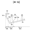
図3A〜図3Cは、複数の傾斜面を有する第2のリフレクタ上に配置された反射構造物を示す図である。 FIG. 3A to FIG. 3C are diagrams illustrating a reflecting structure disposed on a second reflector having a plurality of inclined surfaces.
図3Aでは、互いに隣接する2つの傾斜面が平らな表面を有し、図3Bでは、互いに隣接する2つの傾斜面が凹状の曲面を有し、2つの傾斜面の曲率は互いに異なり得る。また、図3Cでは、互いに隣接する2つの傾斜面が凸状の曲面を有し、2つの傾斜面の曲率は互いに異なり得る。 In FIG. 3A, the two inclined surfaces adjacent to each other have a flat surface, and in FIG. 3B, the two inclined surfaces adjacent to each other have a concave curved surface, and the curvatures of the two inclined surfaces may be different from each other. In FIG. 3C, two inclined surfaces adjacent to each other have convex curved surfaces, and the curvatures of the two inclined surfaces may be different from each other.
図3A〜図3Cに示すように、第2のリフレクタ300は、光源モジュール100に隣接した第1の領域300a、光源モジュール100から離隔した第3の領域300c、及び第1の領域300aと第3の領域300cとの間に位置する第2の領域300bを有することができる。
3A to 3C, the
ここで、第2のリフレクタ300の第1の領域300aは傾斜面で、第2の領域300bは傾斜面及び平面を有し、第3の領域300cは平面であり得る。
Here, the
そして、反射構造物400は、第2のリフレクタ300の第2及び第3の領域300b、300cのうちの少なくとも1ヶ所に配置することができる。
The
このように、反射構造物400は、第2のリフレクタ300の全体領域のうち輝度が相対的に低い第2及び第3の領域300b、300cに配置することによって、光を反射及び拡散させ、低い輝度を補償することができる。
As described above, the
図4Aは、ストライプ状を有する反射構造物を示す斜視図で、図4Bは、第2のリフレクタに配置された反射構造物を示す平面図である。 FIG. 4A is a perspective view illustrating a reflective structure having a stripe shape, and FIG. 4B is a plan view illustrating the reflective structure disposed on the second reflector.
図4A及び図4Bに示すように、ストライプ状の反射構造物400は、反射部410及び支持部420を有しているが、反射部410は、反射物質がコーティングされた反射体、光繊維、又はCCFL(Cold Cathode Fluorescent Lamp:冷陰極蛍光ランプ)などのような光源であってもよい。
As shown in FIGS. 4A and 4B, the stripe-shaped
ここで、反射部410はストライプ状であって、1つの反射部410を光源モジュール100と同一方向に平行に配列することができる。
Here, the
そして、支持部420は、反射部410の下部に複数配置され、反射部410を支持することができる。
A plurality of
ここで、支持部420は、表面に反射物質がコーティングされることによって、光を反射させることもできる。
Here, the
図5Aは、ドット状を有する反射構造物を示す斜視図で、図5Bは、第2のリフレクタに配置された反射構造物を示す平面図である。 FIG. 5A is a perspective view showing a reflective structure having a dot shape, and FIG. 5B is a plan view showing the reflective structure arranged on the second reflector.
図5A及び図5Bに示すように、ドット状の反射構造物400は、反射部410及び支持部420を有しているが、反射部410は反射物質がコーティングされた反射体であり得る。
As shown in FIGS. 5A and 5B, the dot-like
ここで、反射部410はドット状であって、複数の反射部410を光源モジュール100と同一方向に並んで配列することができる。
Here, the
そして、1つの支持部420は、1つの反射部410の下部に1対1で対応するように配置され、反射部410を支持することができる。
One
ここで、支持部420は、表面に反射物質がコーティングされることによって、光を反射させることもできる。
Here, the
このように、反射部410と支持部420は、図5Aに示すように、1対1の比率で対応して配置したり、又は、図4Aのように、1対複数の比率で対応して配置することができる。
As described above, the
図6A〜図6Fは反射構造物の反射部の形状を示す図である。 6A to 6F are views showing the shape of the reflecting portion of the reflecting structure.
まず、図6Aに示すように、支持部420によって支持される反射部410は、断面が円状であってもよく、場合に応じて楕円状であってもよい。
First, as illustrated in FIG. 6A, the
そして、図6Bに示すように、反射部410の安定感のために、反射部410の断面は、下部面が平らで、上部面が丸い半円状であってもよい。
As shown in FIG. 6B, for the stability of the
そして、図6Cに示すように、特定方向に光を反射させるために、反射部410の断面は、三角形状であってもよく、場合に応じて逆三角形状であってもよい。
Then, as shown in FIG. 6C, in order to reflect light in a specific direction, the cross section of the reflecting
次に、図6D、図6E、図6Fに示すように、反射部410の断面は多角形状であってもよい。
Next, as shown in FIGS. 6D, 6E, and 6F, the cross section of the
ここで、多角形状は、正方形状、長方形状、台形状、菱形状を含むこともでき、4個以上の角を有する多角形状を含むこともできる。 Here, the polygonal shape may include a square shape, a rectangular shape, a trapezoidal shape, and a rhombus shape, and may also include a polygonal shape having four or more corners.
図7A及び図7Bは、複数の微細突起を有する反射部を示す図である。 7A and 7B are diagrams showing a reflecting portion having a plurality of fine protrusions.
図7Aに示すように、反射構造物の反射部410の表面には複数の微細突起412を形成することができる。
As shown in FIG. 7A, a plurality of
ここで、複数の微細突起412は反射部410の表面全体に配置できるが、互いに隣接する各微細突起412は、一定間隔だけ離隔するように配置することができ、一列に並んで配列することもできる。
Here, the plurality of
場合に応じては、図7Bに示すように、複数の微細突起412は、反射部410の表面全体に配置できるが、互いに隣接する各微細突起412は、一定間隔だけ離隔するように配置することができ、交互に配列することもできる。
Depending on the case, as shown in FIG. 7B, the plurality of
ここで、各微細突起412は、反射物質がコーティングされた反射体であって、光を反射及び拡散させることによって、均一な輝度を提供することができる。
Here, each
図8A及び図8Bは、複数の微細溝を有する反射部を示す図である。 8A and 8B are diagrams showing a reflecting portion having a plurality of fine grooves.
図8Aに示すように、反射構造物の反射部410の表面には複数の微細溝414を形成することができる。
As shown in FIG. 8A, a plurality of
ここで、複数の微細溝414は反射部410の表面全体に配置できるが、互いに隣接する各微細溝414は、一定間隔だけ離隔するように配置することができ、一列に並んで配列することもできる。
Here, although the plurality of
場合に応じては、図8Bに示すように、複数の微細溝414は反射部410の表面全体に配置できるが、互いに隣接する各微細溝414は、一定間隔だけ離隔するように配置することができ、交互に配列することもできる。
In some cases, as shown in FIG. 8B, the plurality of
ここで、各微細溝414は、反射物質がコーティングされた反射体であって、光を反射及び拡散させることによって、均一な輝度を提供することができる。
Here, each of the
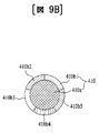
図9A〜図9Dは、反射層が形成された反射部を示す断面図であって、図9A及び図9Bは、反射部の全体表面にコーティングされた反射層を示す図で、図9C及び図9Dは、反射部の一部表面にコーティングされた反射層を示す図である。 9A to 9D are cross-sectional views showing the reflective portion on which the reflective layer is formed, and FIGS. 9A and 9B are diagrams showing the reflective layer coated on the entire surface of the reflective portion. 9D is a diagram showing a reflective layer coated on a partial surface of the reflective portion.
図9A〜図9Dに示すように、反射部410は、コア410aと、コア410aの全体表面又は一部表面を取り囲む反射層410bとを備えることができる。
As shown in FIGS. 9A to 9D, the
ここで、コア410aは、射出可能なプラスチックなどの高分子樹脂を用いて製作することができる。
Here, the
そして、反射層410bは、フィルム状に製作された反射コーティングフィルムであってもよく、反射物質が蒸着された反射コーティング物質層であってもよい。
The
また、反射層410bは、金属又は金属酸化物のうちの少なくとも1つを含むことができ、例えば、アルミニウム(Al)、銀(Ag)、金(Au)又は二酸化チタン(TiO2)のように高い反射率を有する金属又は金属酸化物を含んで構成することができる。
The
この場合、反射層410bは、金属又は金属酸化物を高分子樹脂であるコア410a上に蒸着又はコーティングして形成することができ、金属インクを印刷して形成することもできる。
In this case, the
ここで、蒸着方法としては、熱蒸着法、蒸発法又はスパッタリング法などの真空蒸着法を使用することができ、コーティング又は印刷方法としては、プリンティング法、グラビアコーティング法又はシルクスクリーン法を使用することができる。 Here, a vacuum evaporation method such as a thermal evaporation method, an evaporation method or a sputtering method can be used as the evaporation method, and a printing method, a gravure coating method or a silk screen method can be used as a coating or printing method. Can do.
また、反射層410bは、フィルム又はシート状に製作し、高分子樹脂のコア410a上に接着剤で接着することもできる。
Alternatively, the
このように、反射部410は、図9Aに示すように、コア410aと、コア410aの全体表面を取り囲む単一の反射層410bとを備えることができるので、反射部410は全体的に同一の反射率を有することができる。
As described above, as shown in FIG. 9A, the
そして、反射部410は、図9Bに示すように、コア410aと、コア410aの全体表面を取り囲む複数の反射層410b1、410b2、410b3、410b4、410b5を備えることができるので、反射部410は複数の反射率を有することもできる。
As shown in FIG. 9B, the
また、反射部410は、図9Cに示すように、コア410aと、コア410aの一部表面のみに形成された反射層410bとを備えることができる。
Moreover, the
ここで、反射層410bは、コア410aの一部表面が露出するように、コア410aの一部表面から突出形成することができる。
Here, the
場合に応じて、反射部410は、図9Dに示すように、複数の溝を有するコア410aと、コア410aの溝内に形成された反射層410bとを備えることができる。
As shown in FIG. 9D, the
ここで、反射層410bは、コア410aの一部表面が露出するように、コア410aの溝内に挿入して形成することもできる。
Here, the
このように、反射層410bは、同一の反射率を有する1つの反射物質又は互いに異なる反射率を有する複数の反射物質からなり得る。
As described above, the
そして、反射層410bは、コア410aの表面から突出したり、又はコア410aの表面内に挿入することもできる。
The
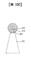
図10A〜図10Dは、反射部と支持部を結合する結合部材を示す図である。 10A to 10D are diagrams illustrating a coupling member that couples the reflection portion and the support portion.
図10Aに示すように、反射構造物は反射部410及び支持部420を有するが、反射部410は、結合部材422によって支持部420の上部表面上に安定的に結合することができる。
As shown in FIG. 10A, the reflective structure includes a
ここで、結合部材422は、支持部420の上部面に付着され、反射部410の下部面を支持する板状であってもよい。
Here, the
そして、図10Bに示すように、結合部材422は、支持部420の上部面に付着され、反射部410の周囲を取り囲むリング状であってもよい。
10B, the
そして、図10Cに示すように、結合部材422は、支持部420の上部面に付着され、反射部410の溝414内に挿入される突出形状であってもよい。
10C, the
そして、図10Dに示すように、反射部410と支持部420は、結合部材422の代わりに接着剤424によって付着することもできる。
Then, as shown in FIG. 10D, the
図11は、反射構造物の反射部と支持部の幅と高さを比較した図である。 FIG. 11 is a diagram comparing the width and height of the reflecting portion and the supporting portion of the reflecting structure.
図11に示すように、支持部420は、反射部410を安定的に支持するために、下部が上部より大きい厚さを有することができる。
As shown in FIG. 11, the
すなわち、支持部420の下部厚さt2は、支持部420の上部厚さt1より大きくなり得る。
That is, the lower thickness t2 of the
場合に応じて、支持部420の下部厚さt2と支持部420の上部厚さt1が互いに同一であってもよい。
According to circumstances, the lower thickness t2 of the
そして、支持部420の下部面の幅W2は、反射部410の上部面の幅W1より大きくなり得る。
The width W2 of the lower surface of the
場合に応じて、支持部420の下部面の幅W2と反射部410の上部面の幅W1が互いに同一であってもよい。
Depending on the case, the width W2 of the lower surface of the
また、支持部420の高さH1は反射部410の高さH2より大きくなり得る。また、場合に応じて、支持部420の高さH1と反射部410の高さH2は互いに同一であってもよい。
Further, the height H1 of the
ここで、支持部420の高さは、反射部410が光源モジュールと同一線上に位置するように可変になり得る。
Here, the height of the
反射部410を光源モジュールと同一線上に位置させる理由は、そうすると、反射部410と光源モジュールとの距離が最も近くなるので、光を効果的に反射させることができ、輝度を最大に補償できるためである。
The reason why the reflecting
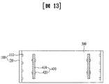
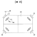
図12は、1エッジタイプの第2のリフレクタに配置された反射構造物を示す図で、図13は、2エッジタイプの第2のリフレクタに配置された反射構造物を示す図で、図14及び図15は、4エッジタイプの第2のリフレクタに配置された反射構造物を示す図である。 FIG. 12 is a diagram illustrating a reflective structure disposed on a two-edge type second reflector, and FIG. 13 is a diagram illustrating a reflective structure disposed on a two-edge type second reflector. FIGS. 15A and 15B are diagrams showing a reflective structure arranged in a four-edge type second reflector.
図12は、1エッジタイプの第2のリフレクタに配置された反射構造物を示す平面図であって、図12に示すように、1エッジタイプの第2のリフレクタ300の一側に光源モジュール100を配置し、反射構造物400は、第2のリフレクタ300の一定領域上に配置することができる。
FIG. 12 is a plan view showing a reflecting structure arranged in a one-edge type second reflector, and as shown in FIG. 12, a
そして、図13は、2エッジタイプの第2のリフレクタに配置された反射構造物を示す平面図であって、図13に示すように、2エッジタイプの第2のリフレクタ300の両側に光源モジュール100を配置し、第2のリフレクタ300は光源モジュール100に対応する第1の領域と第2の領域に分離し、反射構造物400は、第2のリフレクタ300の第1の領域と第2の領域に配置することができる。
FIG. 13 is a plan view showing the reflecting structure disposed on the two-edge type second reflector. As shown in FIG. 13, the light source modules are arranged on both sides of the two-edge type
そして、図14は、4エッジタイプの第2のリフレクタに配置された反射構造物を示す平面図であって、図14に示すように、4エッジタイプの第2のリフレクタ300の4側面に光源モジュール100を配置し、第2のリフレクタ300は第1の光源モジュール100に対応する第1、第2、第3及び第4の領域に分離し、反射構造物400は、第2のリフレクタ300の第1、第2、第3及び第4の領域に配置することができる。
FIG. 14 is a plan view showing the reflecting structure disposed on the four-edge type second reflector. As shown in FIG. 14, light sources are provided on the four side surfaces of the four-edge type
そして、図15は、4エッジタイプの第2のリフレクタに配置された反射構造物を示す平面図であって、図15に示すように、4エッジタイプの第2のリフレクタ300の4つのコーナー領域に光源モジュール100を配置し、第2のリフレクタ300は光源モジュール100に対応する第1、第2、第3及び第4の領域に分離し、反射構造物400は、第2のリフレクタ300の第1、第2、第3及び第4の領域に配置することができる。
FIG. 15 is a plan view showing a reflecting structure arranged on the four-edge type second reflector, and as shown in FIG. 15, four corner regions of the four-edge type
また、本発明の一実施例に係るバックライトユニットは、第2のリフレクタから一定間隔だけ空間を置いて配置された光学部材をさらに備えることができ、第2のリフレクタと光学部材との間の空間にはエアガイドを形成することができる。 In addition, the backlight unit according to an embodiment of the present invention may further include an optical member disposed at a predetermined interval from the second reflector, and the backlight unit may be provided between the second reflector and the optical member. An air guide can be formed in the space.
図16は、光学部材を備えるバックライトユニットを示す図である。 FIG. 16 is a diagram illustrating a backlight unit including an optical member.
図16に示すように、光学部材600は、第1のリフレクタ200のオープン領域に配置し、上部表面に凹凸パターン620を有することができる。
As shown in FIG. 16, the
ここで、光学部材600は、第1のリフレクタ200のオープン領域を通して出射される光を拡散させるためのものであって、拡散効果を増加させるために、光学部材600の上部表面に凹凸パターン620を形成することができる。
Here, the
すなわち、光学部材600は多層に形成することができ、凹凸パターン620は最上層又はいずれか1つの層の表面に備えることができる。
That is, the
そして、凹凸パターン620は、光源モジュール100に沿って配置されるストライプ状を有することができる。
The
このとき、凹凸パターン620は、光学部材600の表面に突出部を有し、突出部は、互いに対向する第1の面及び第2の面を含んで構成され、第1の面と第2の面との間の角は鈍角又は鋭角であり得る。
At this time, the concavo-
場合に応じて、光学部材600は、少なくとも1つのシートからなるが、拡散シート、プリズムシート、輝度強化シートなどを選択的に含むことができる。
Depending on the case, the
ここで、拡散シートは、光源から出射された光を拡散させ、プリズムシートは、拡散された光を発光領域にガイドし、輝度拡散シートは輝度を強化させる。 Here, the diffusion sheet diffuses the light emitted from the light source, the prism sheet guides the diffused light to the light emitting region, and the luminance diffusion sheet enhances the luminance.
一方、反射部410及び支持部420を含む反射構造物400は、光学部材600から第1の間隔d1だけ離隔するように配置することができる。
On the other hand, the
ここで、第1の間隔d1は、第1のリフレクタ200の厚さTより大きくなり得る。
Here, the first distance d <b> 1 may be larger than the thickness T of the
反射構造物400を光学部材600から第1の間隔d1だけ離隔して配置させる理由は、反射構造物400が光学部材600に近く配置されると、黒いラインのような暗部が発生し、輝度が低下するおそれがあるためである。
The reason for disposing the
したがって、反射構造物400は、第1のリフレクタ200から水平に延長される水平延長線と第2のリフレクタ300との間に位置することができる。
Accordingly, the
そして、反射構造物400の反射部410は、光源モジュール100の光源110と同一線上A1に位置することができる。
The
その理由は、そうすると、反射部410と光源モジュール100の光源110との距離が最も近いので、反射部410は光を効果的に反射させることができ、輝度を最大に補償できるためである。
The reason for this is that, since the distance between the
このように、バックライトユニットは、第2のリフレクタ上に反射構造物をさらに配置することによって、輝度を向上させ、均一な輝度を提供することができる。 As described above, the backlight unit can further improve the luminance and provide uniform luminance by disposing the reflective structure on the second reflector.
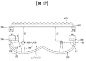
図17は、支持フレームによって支持される光学部材を示す図である。 FIG. 17 is a diagram illustrating an optical member supported by a support frame.
図17に示すように、第1のリフレクタ200の上部には、光学部材600を支持するための支持フレーム500をさらに形成することができる。
As shown in FIG. 17, a
そして、光学部材600は、支持フレーム500によって支持されることによって、第2のリフレクタ300と光学部材600との間の空間をさらに確保することができる。
Further, the
このように、支持フレーム500によって、第2のリフレクタ300と光学部材600との間の空間がさらに確保されると、光を拡散させるための空間であるエアガイドを通して均一な輝度を得ることができる。
As described above, when the space between the
ここで、支持フレーム500の幅W2は、第1のリフレクタ200の幅W1より小さいか又は同一であり得る。
Here, the width W2 of the
その理由は、支持フレーム500による輝度領域の減少を防止するためである。
The reason for this is to prevent a reduction in the luminance region due to the
そして、反射部410及び支持部420を含む反射構造物400は、光学部材600から第2の間隔d2だけ離隔するように配置することができる。
The
ここで、第2の間隔d2は、第1のリフレクタ200の厚さTより大きくなり得る。
Here, the second distance d <b> 2 may be larger than the thickness T of the
このように、反射構造物400と光学部材600との間の間隔が大きいと、黒いラインのような暗部が表れないので、均一な輝度を提供することができる。
As described above, when the distance between the
そして、反射構造物400の反射部410は、光源モジュール100の光源110と同一線上A1に位置することができる。
The
その理由は、そうすると、反射部410と光源モジュール100の光源110との距離が最も近いので、反射部410は光を効果的に反射させることができ、輝度を最大に補償できるためである。
The reason for this is that, since the distance between the
このように、バックライトユニットは、第2のリフレクタ上に反射構造物をさらに配置することによって、輝度を向上させ、均一な輝度を提供することができる。 As described above, the backlight unit can further improve the luminance and provide uniform luminance by disposing the reflective structure on the second reflector.
このように、各実施例は、導光板を使用せずに、反射構造物が配置されたエアガイド用リフレクタを形成することによって、重さが軽く、製作単価が低廉であり、均一な輝度を提供することができる。 As described above, in each embodiment, without using a light guide plate, by forming a reflector for an air guide in which a reflecting structure is arranged, the weight is light, the manufacturing unit price is low, and uniform brightness is achieved. Can be provided.
したがって、バックライトユニットの経済性及び信頼性を向上させることができる。 Therefore, the economical efficiency and reliability of the backlight unit can be improved.
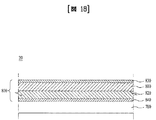
図18は、実施例に係るバックライトユニットを有するディスプレイモジュールを示す図である。 FIG. 18 is a diagram illustrating a display module having a backlight unit according to an embodiment.
図18に示すように、ディスプレイモジュール20は、ディスプレイパネル800及びバックライトユニット700を備えることができる。
As shown in FIG. 18, the
ディスプレイパネル800は、互いに対向して均一なセルギャップが維持されるように合着されたカラーフィルター基板810とTFT(Thin Film Transistor)基板820を含み、前記二つの基板810、820の間に液晶層(図示せず)が介在し得る。
The
そして、ディスプレイパネル800の上側及び下側にはそれぞれ上部偏光板830及び下部偏光板840を配置することができ、より詳細には、カラーフィルター基板810の上面に上部偏光板830を配置し、TFT基板820の下面に下部偏光板840を配置することができる。
An upper
図面に図示していないが、ディスプレイパネル800の側面には、パネル800を駆動させるための駆動信号を生成するゲート及びデータ駆動部を備えることができる。
Although not shown in the drawing, the side surface of the
図19及び図20は、本発明の一実施例に係るディスプレイ装置を示す図である。 19 and 20 are diagrams illustrating a display apparatus according to an embodiment of the present invention.
図19を参照すると、ディスプレイ装置1は、ディスプレイモジュール20と、ディスプレイモジュール20を取り囲むフロントカバー30及びバックカバー35と、バックカバー35に備えられた駆動部55と、駆動部55を取り囲む駆動部カバー40とを備えて構成することができる。
Referring to FIG. 19, the display device 1 includes a
フロントカバー30は、光を透過させる透明な材質の前面パネル(図示せず)を備えることができ、前面パネルは、一定の間隔を置いてディスプレイモジュール20を保護し、ディスプレイモジュール20から放出される光を透過させ、ディスプレイモジュール20で表示される映像が外部で見えるようにする。
The
バックカバー35は、フロントカバー30と結合してディスプレイモジュール20を保護することができる。
The
バックカバー35の一面には駆動部55を配置することができる。
A
駆動部55は、駆動制御部55a、メインボード55b及び電源供給部55cを備えることができる。
The
駆動制御部55aは、タイミングコントローラーとして、ディスプレイモジュール20の各ドライバーICの動作タイミングを調節する駆動部であって、メインボード55bは、タイミングコントローラーにVシンク、Hシンク及びR、G、B解像度信号を伝達する駆動部であって、電源供給部55cは、ディスプレイモジュール20に電源を印加する駆動部である。
The
駆動部55は、バックカバー35に備えられ、駆動部カバー40によって取り囲むことができる。
The
バックカバー35は、複数のホールを備えており、これらホールによってディスプレイモジュール20と駆動部55を連結することができ、ディスプレイ装置1を支持するスタンド60を備えることができる。
The
一方、図20に示すように、駆動部55の駆動制御部55aはバックカバー35に備え、メインボード55bと電源ボード55cはスタンド60に備えることもできる。
On the other hand, as shown in FIG. 20, the
そして、駆動部カバー40は、バックカバー35に備えられた駆動部55のみを取り囲むことができる。
The
本発明の一実施例では、メインボード55bと電源ボード55cをそれぞれ別途に構成したが、これに限定されることはなく、メインボード550bと電源ボード550cを一つの統合ボードで構成することもできる。
In one embodiment of the present invention, the main board 55b and the
更に他の実施例は、上述した各実施例に記載された第1及び第2のリフレクタ及び光源モジュールを備える表示装置、指示装置、照明システムで具現することができ、例えば、照明システムはランプ、街路灯を含むことができる。 Still another embodiment may be implemented by a display device, a pointing device, and a lighting system including the first and second reflectors and the light source module described in each of the above embodiments. For example, the lighting system may be a lamp, Street lights can be included.
このような照明システムは、複数のLEDを集束して光を得る照明灯として使用可能なものであって、特に、建物の天井や壁体内に埋め込まれ、シェードの開口部側が露出するように装着できるようにする埋込灯(ダウンライト)として用いることができる。 Such an illumination system can be used as an illuminating lamp that converges a plurality of LEDs to obtain light, and is particularly embedded in the ceiling or wall of a building and is mounted so that the opening side of the shade is exposed. It can be used as an embedded lamp (downlight) that can be made.
このように、各実施例は、導光板を使用せずに、反射構造物が配置されたエアガイド用リフレクタを形成することによって、重さが軽く、製作単価が低廉であり、均一な輝度を提供することができる。 As described above, in each embodiment, without using a light guide plate, by forming a reflector for an air guide in which a reflecting structure is arranged, the weight is light, the manufacturing unit price is low, and uniform brightness is achieved. Can be provided.
したがって、バックライトユニットの経済性及び信頼性を向上させることができる。 Therefore, the economical efficiency and reliability of the backlight unit can be improved.
100 光源モジュール
110 光源
120 基板
200 第1のリフレクタ
300 第2のリフレクタ
400 反射構造物
410 反射部
420 支持部
DESCRIPTION OF
Claims (25)
一部に傾斜面を有する第2のリフレクタと、
前記第1及び第2のリフレクタの間に配置された少なくとも1つの光源モジュールと、
前記第2のリフレクタに配置された少なくとも1つの反射構造物と
を備えるバックライトユニット。 A first reflector;
A second reflector having a partly inclined surface;
At least one light source module disposed between the first and second reflectors;
A backlight unit comprising: at least one reflective structure disposed on the second reflector.
光を反射させる反射部と、
前記反射部を支持する支持部と
を備える、請求項1乃至5のいずれかに記載のバックライトユニット。 The reflective structure is
A reflection part for reflecting light;
The backlight unit according to claim 1, further comprising a support portion that supports the reflection portion.
コアと、
前記コアの全体又は一部を取り囲む反射層と
を備える、請求項7に記載のバックライトユニット。 The reflective portion is
The core,
The backlight unit according to claim 7, further comprising a reflective layer surrounding the whole or a part of the core.
前記ディスプレイパネルに光を照射するバックライトユニットと
を備え、
前記バックライトユニットは、請求項1乃至5のいずれかに記載のバックライトユニットである、ディスプレイ装置。 A display panel;
A backlight unit for irradiating the display panel with light;
The display device according to claim 1, wherein the backlight unit is the backlight unit according to claim 1.
Applications Claiming Priority (2)
| Application Number | Priority Date | Filing Date | Title |
|---|---|---|---|
| KR10-2011-0071283 | 2011-07-19 | ||
| KR1020110071283A KR101824037B1 (en) | 2011-07-19 | 2011-07-19 | display apparatus |
Publications (2)
| Publication Number | Publication Date |
|---|---|
| JP2013026211A true JP2013026211A (en) | 2013-02-04 |
| JP2013026211A5 JP2013026211A5 (en) | 2015-03-19 |
Family
ID=45656618
Family Applications (1)
| Application Number | Title | Priority Date | Filing Date |
|---|---|---|---|
| JP2012029678A Pending JP2013026211A (en) | 2011-07-19 | 2012-02-14 | Backlight unit and display device using the same |
Country Status (6)
| Country | Link |
|---|---|
| US (1) | US8931911B2 (en) |
| EP (1) | EP2549308B1 (en) |
| JP (1) | JP2013026211A (en) |
| KR (1) | KR101824037B1 (en) |
| CN (1) | CN102889508B (en) |
| TW (1) | TWI652531B (en) |
Families Citing this family (3)
| Publication number | Priority date | Publication date | Assignee | Title |
|---|---|---|---|---|
| KR101852389B1 (en) * | 2011-10-25 | 2018-04-26 | 엘지이노텍 주식회사 | Display |
| KR102161512B1 (en) * | 2014-01-06 | 2020-10-05 | 엘지전자 주식회사 | backlight unit |
| KR20160098921A (en) * | 2015-02-11 | 2016-08-19 | 엘지전자 주식회사 | Backlight unit and display apparatus comprising the same |
Citations (11)
| Publication number | Priority date | Publication date | Assignee | Title |
|---|---|---|---|---|
| JP2002116705A (en) * | 2000-10-11 | 2002-04-19 | Tama Electric Co Ltd | Backlight device |
| JP2004296298A (en) * | 2003-03-27 | 2004-10-21 | Nec Lcd Technologies Ltd | Backlight device and liquid crystal display |
| JP2006003732A (en) * | 2004-06-18 | 2006-01-05 | Sharp Corp | Illuminator for display device |
| JP2006106212A (en) * | 2004-10-01 | 2006-04-20 | Nippon Leiz Co Ltd | Backlight unit |
| US20070171676A1 (en) * | 2006-01-20 | 2007-07-26 | Hon Hai Precision Industry Co., Ltd. | Backlight module |
| JP2008152933A (en) * | 2006-12-14 | 2008-07-03 | Takehisa Saito | Surface light-emitting device and light-emitting type signboard |
| JP2008191237A (en) * | 2007-02-01 | 2008-08-21 | Ips Alpha Technology Ltd | Liquid crystal display |
| JP2008299174A (en) * | 2007-06-01 | 2008-12-11 | Hitachi Ltd | Video display device and backlight unit used for the same |
| JP2009134992A (en) * | 2007-11-30 | 2009-06-18 | Sharp Corp | Backlight device |
| JP2009187904A (en) * | 2008-02-08 | 2009-08-20 | Toppan Printing Co Ltd | Light source unit, back light unit, and display |
| JP2011044425A (en) * | 2009-07-24 | 2011-03-03 | Victor Co Of Japan Ltd | Backlight unit and liquid crystal display device |
Family Cites Families (10)
| Publication number | Priority date | Publication date | Assignee | Title |
|---|---|---|---|---|
| KR100804653B1 (en) | 2003-06-16 | 2008-02-20 | 미쓰비시덴키 가부시키가이샤 | Planar light source device and display device using the same |
| CN1836133A (en) * | 2003-06-16 | 2006-09-20 | 三菱电机株式会社 | Planar light source device and display device using the same |
| KR20050037085A (en) * | 2003-10-17 | 2005-04-21 | 삼성전자주식회사 | Light tunnel, illuminating device and projector adopting the same |
| JP2005129409A (en) | 2003-10-24 | 2005-05-19 | Sanyo Electric Co Ltd | Backlight apparatus |
| US7284893B2 (en) * | 2005-03-09 | 2007-10-23 | K-Bridge Electronics Co., Ltd. | Light equalizing structure of backlight modules |
| US8197105B2 (en) * | 2009-08-13 | 2012-06-12 | Intematix Corporation | LED-based lamps |
| CN102576119B (en) | 2009-10-24 | 2014-03-26 | 3M创新有限公司 | Light source and display system incorporating same |
| KR101604497B1 (en) * | 2009-12-08 | 2016-03-17 | 엘지디스플레이 주식회사 | Backlight unit and liquid crystal display device having the same |
| US8382324B2 (en) * | 2010-04-29 | 2013-02-26 | Southern Taiwan University | Radiation structure without light guiding board |
| KR101040654B1 (en) * | 2010-05-28 | 2011-06-10 | 엘지이노텍 주식회사 | Backlight unit and display device including the same |
-
2011
- 2011-07-19 KR KR1020110071283A patent/KR101824037B1/en active IP Right Grant
-
2012
- 2012-02-10 US US13/370,580 patent/US8931911B2/en active Active
- 2012-02-14 TW TW101104672A patent/TWI652531B/en not_active IP Right Cessation
- 2012-02-14 JP JP2012029678A patent/JP2013026211A/en active Pending
- 2012-02-24 EP EP12156819.0A patent/EP2549308B1/en not_active Not-in-force
- 2012-03-21 CN CN201210076471.1A patent/CN102889508B/en not_active Expired - Fee Related
Patent Citations (11)
| Publication number | Priority date | Publication date | Assignee | Title |
|---|---|---|---|---|
| JP2002116705A (en) * | 2000-10-11 | 2002-04-19 | Tama Electric Co Ltd | Backlight device |
| JP2004296298A (en) * | 2003-03-27 | 2004-10-21 | Nec Lcd Technologies Ltd | Backlight device and liquid crystal display |
| JP2006003732A (en) * | 2004-06-18 | 2006-01-05 | Sharp Corp | Illuminator for display device |
| JP2006106212A (en) * | 2004-10-01 | 2006-04-20 | Nippon Leiz Co Ltd | Backlight unit |
| US20070171676A1 (en) * | 2006-01-20 | 2007-07-26 | Hon Hai Precision Industry Co., Ltd. | Backlight module |
| JP2008152933A (en) * | 2006-12-14 | 2008-07-03 | Takehisa Saito | Surface light-emitting device and light-emitting type signboard |
| JP2008191237A (en) * | 2007-02-01 | 2008-08-21 | Ips Alpha Technology Ltd | Liquid crystal display |
| JP2008299174A (en) * | 2007-06-01 | 2008-12-11 | Hitachi Ltd | Video display device and backlight unit used for the same |
| JP2009134992A (en) * | 2007-11-30 | 2009-06-18 | Sharp Corp | Backlight device |
| JP2009187904A (en) * | 2008-02-08 | 2009-08-20 | Toppan Printing Co Ltd | Light source unit, back light unit, and display |
| JP2011044425A (en) * | 2009-07-24 | 2011-03-03 | Victor Co Of Japan Ltd | Backlight unit and liquid crystal display device |
Also Published As
| Publication number | Publication date |
|---|---|
| EP2549308A3 (en) | 2013-04-17 |
| KR20130010574A (en) | 2013-01-29 |
| CN102889508B (en) | 2016-07-27 |
| US20130021779A1 (en) | 2013-01-24 |
| US8931911B2 (en) | 2015-01-13 |
| TW201305683A (en) | 2013-02-01 |
| TWI652531B (en) | 2019-03-01 |
| EP2549308B1 (en) | 2016-08-17 |
| CN102889508A (en) | 2013-01-23 |
| KR101824037B1 (en) | 2018-01-31 |
| EP2549308A2 (en) | 2013-01-23 |
Similar Documents
| Publication | Publication Date | Title |
|---|---|---|
| JP6163232B2 (en) | Backlight unit and display device using the same | |
| JP5406225B2 (en) | Backlight unit | |
| JP6062083B2 (en) | Lighting system | |
| JP6061513B2 (en) | Light unit and lighting system using the same | |
| JP6116805B2 (en) | Backlight unit, display device using the same, and illumination system including the same | |
| JP2013026211A (en) | Backlight unit and display device using the same | |
| JP5868934B2 (en) | Backlight unit and display device using the same | |
| KR101827976B1 (en) | Backlight unit, display using the same, and lighting apparatus including the same | |
| KR20130020302A (en) | Backlight unit and display apparatus using the same | |
| KR101850436B1 (en) | display device and illumination system using the same | |
| KR101868536B1 (en) | Illumination system | |
| KR101948139B1 (en) | backlight unit and illumination system using the same | |
| KR101850429B1 (en) | backlight unit and display apparatus using the same | |
| KR101908652B1 (en) | backlight unit and display apparatus using the same | |
| KR20130002802A (en) | Backlight unit and display apparatus using the same | |
| KR20130070859A (en) | Backlight unit and illumination system using the same | |
| KR20130058515A (en) | Backlight unit and illumination system using the same | |
| KR20130020303A (en) | Backlight unit and display apparatus using the same |
Legal Events
| Date | Code | Title | Description |
|---|---|---|---|
| A521 | Written amendment |
Free format text: JAPANESE INTERMEDIATE CODE: A523 Effective date: 20150129 |
|
| A621 | Written request for application examination |
Free format text: JAPANESE INTERMEDIATE CODE: A621 Effective date: 20150129 |
|
| A977 | Report on retrieval |
Free format text: JAPANESE INTERMEDIATE CODE: A971007 Effective date: 20151225 |
|
| A131 | Notification of reasons for refusal |
Free format text: JAPANESE INTERMEDIATE CODE: A131 Effective date: 20160105 |
|
| A521 | Written amendment |
Free format text: JAPANESE INTERMEDIATE CODE: A523 Effective date: 20160323 |
|
| A02 | Decision of refusal |
Free format text: JAPANESE INTERMEDIATE CODE: A02 Effective date: 20160614 |