JP2014127630A - Reflective mask blank for euv lithography and manufacturing method thereof - Google Patents
Reflective mask blank for euv lithography and manufacturing method thereof Download PDFInfo
- Publication number
- JP2014127630A JP2014127630A JP2012284649A JP2012284649A JP2014127630A JP 2014127630 A JP2014127630 A JP 2014127630A JP 2012284649 A JP2012284649 A JP 2012284649A JP 2012284649 A JP2012284649 A JP 2012284649A JP 2014127630 A JP2014127630 A JP 2014127630A
- Authority
- JP
- Japan
- Prior art keywords
- layer
- film
- mask blank
- multilayer reflective
- protective layer
- Prior art date
- Legal status (The legal status is an assumption and is not a legal conclusion. Google has not performed a legal analysis and makes no representation as to the accuracy of the status listed.)
- Withdrawn
Links
- 238000001900 extreme ultraviolet lithography Methods 0.000 title claims abstract description 45
- 238000004519 manufacturing process Methods 0.000 title claims abstract description 31
- 238000010521 absorption reaction Methods 0.000 claims abstract description 125
- 229910052757 nitrogen Inorganic materials 0.000 claims abstract description 107
- 239000000758 substrate Substances 0.000 claims abstract description 39
- 229910052715 tantalum Inorganic materials 0.000 claims abstract description 36
- 150000001875 compounds Chemical class 0.000 claims abstract description 14
- 239000010410 layer Substances 0.000 claims description 584
- 239000010408 film Substances 0.000 claims description 199
- IJGRMHOSHXDMSA-UHFFFAOYSA-N Atomic nitrogen Chemical compound N#N IJGRMHOSHXDMSA-UHFFFAOYSA-N 0.000 claims description 146
- 239000011241 protective layer Substances 0.000 claims description 135
- 238000000034 method Methods 0.000 claims description 90
- 239000012298 atmosphere Substances 0.000 claims description 79
- 239000010409 thin film Substances 0.000 claims description 58
- QJGQUHMNIGDVPM-UHFFFAOYSA-N nitrogen group Chemical group [N] QJGQUHMNIGDVPM-UHFFFAOYSA-N 0.000 claims description 45
- 238000007689 inspection Methods 0.000 claims description 38
- 229910052710 silicon Inorganic materials 0.000 claims description 37
- 230000015572 biosynthetic process Effects 0.000 claims description 27
- 229910052760 oxygen Inorganic materials 0.000 claims description 20
- 229910003071 TaON Inorganic materials 0.000 claims description 14
- 229910004535 TaBN Inorganic materials 0.000 claims description 6
- 229910004200 TaSiN Inorganic materials 0.000 claims description 5
- 239000000203 mixture Substances 0.000 abstract description 23
- 230000008021 deposition Effects 0.000 abstract description 15
- 239000012528 membrane Substances 0.000 abstract 2
- 239000007789 gas Substances 0.000 description 61
- 229910001873 dinitrogen Inorganic materials 0.000 description 38
- XKRFYHLGVUSROY-UHFFFAOYSA-N Argon Chemical compound [Ar] XKRFYHLGVUSROY-UHFFFAOYSA-N 0.000 description 36
- 238000005530 etching Methods 0.000 description 33
- 230000003647 oxidation Effects 0.000 description 31
- 238000007254 oxidation reaction Methods 0.000 description 31
- 229910052786 argon Inorganic materials 0.000 description 20
- 230000003746 surface roughness Effects 0.000 description 19
- 230000007423 decrease Effects 0.000 description 18
- 239000011261 inert gas Substances 0.000 description 17
- 239000000463 material Substances 0.000 description 17
- 230000007547 defect Effects 0.000 description 16
- 238000000151 deposition Methods 0.000 description 15
- 229910052739 hydrogen Inorganic materials 0.000 description 15
- 238000004544 sputter deposition Methods 0.000 description 14
- 230000000694 effects Effects 0.000 description 13
- 238000001659 ion-beam spectroscopy Methods 0.000 description 12
- QVGXLLKOCUKJST-UHFFFAOYSA-N atomic oxygen Chemical compound [O] QVGXLLKOCUKJST-UHFFFAOYSA-N 0.000 description 9
- 238000001755 magnetron sputter deposition Methods 0.000 description 9
- 238000005121 nitriding Methods 0.000 description 9
- 239000001301 oxygen Substances 0.000 description 9
- 229910052796 boron Inorganic materials 0.000 description 8
- 239000011651 chromium Substances 0.000 description 8
- 239000011521 glass Substances 0.000 description 8
- 238000000059 patterning Methods 0.000 description 8
- XUIMIQQOPSSXEZ-UHFFFAOYSA-N Silicon Chemical compound [Si] XUIMIQQOPSSXEZ-UHFFFAOYSA-N 0.000 description 7
- 239000011248 coating agent Substances 0.000 description 7
- 238000000576 coating method Methods 0.000 description 7
- 239000013078 crystal Substances 0.000 description 7
- 238000001312 dry etching Methods 0.000 description 7
- 238000010438 heat treatment Methods 0.000 description 7
- 150000002500 ions Chemical class 0.000 description 7
- 230000007261 regionalization Effects 0.000 description 7
- 239000010703 silicon Substances 0.000 description 7
- 229910052799 carbon Inorganic materials 0.000 description 6
- 239000001257 hydrogen Substances 0.000 description 6
- 239000004065 semiconductor Substances 0.000 description 6
- 230000001133 acceleration Effects 0.000 description 5
- 229910052804 chromium Inorganic materials 0.000 description 5
- 238000000206 photolithography Methods 0.000 description 5
- OKTJSMMVPCPJKN-UHFFFAOYSA-N Carbon Chemical compound [C] OKTJSMMVPCPJKN-UHFFFAOYSA-N 0.000 description 4
- ZAMOUSCENKQFHK-UHFFFAOYSA-N Chlorine atom Chemical compound [Cl] ZAMOUSCENKQFHK-UHFFFAOYSA-N 0.000 description 4
- UFHFLCQGNIYNRP-UHFFFAOYSA-N Hydrogen Chemical compound [H][H] UFHFLCQGNIYNRP-UHFFFAOYSA-N 0.000 description 4
- 239000000460 chlorine Substances 0.000 description 4
- 229910052801 chlorine Inorganic materials 0.000 description 4
- 238000004140 cleaning Methods 0.000 description 4
- 229910052731 fluorine Inorganic materials 0.000 description 4
- 239000012299 nitrogen atmosphere Substances 0.000 description 4
- ZOXJGFHDIHLPTG-UHFFFAOYSA-N Boron Chemical compound [B] ZOXJGFHDIHLPTG-UHFFFAOYSA-N 0.000 description 3
- PXGOKWXKJXAPGV-UHFFFAOYSA-N Fluorine Chemical compound FF PXGOKWXKJXAPGV-UHFFFAOYSA-N 0.000 description 3
- 229910004298 SiO 2 Inorganic materials 0.000 description 3
- 229910010413 TiO 2 Inorganic materials 0.000 description 3
- 238000002441 X-ray diffraction Methods 0.000 description 3
- 230000000052 comparative effect Effects 0.000 description 3
- 239000000470 constituent Substances 0.000 description 3
- 238000012937 correction Methods 0.000 description 3
- 239000011737 fluorine Substances 0.000 description 3
- 229910052759 nickel Inorganic materials 0.000 description 3
- 230000001737 promoting effect Effects 0.000 description 3
- 238000002310 reflectometry Methods 0.000 description 3
- GUVRBAGPIYLISA-UHFFFAOYSA-N tantalum atom Chemical compound [Ta] GUVRBAGPIYLISA-UHFFFAOYSA-N 0.000 description 3
- 229910052727 yttrium Inorganic materials 0.000 description 3
- VYZAMTAEIAYCRO-UHFFFAOYSA-N Chromium Chemical compound [Cr] VYZAMTAEIAYCRO-UHFFFAOYSA-N 0.000 description 2
- ZOKXTWBITQBERF-UHFFFAOYSA-N Molybdenum Chemical compound [Mo] ZOKXTWBITQBERF-UHFFFAOYSA-N 0.000 description 2
- 230000002745 absorbent Effects 0.000 description 2
- 239000002250 absorbent Substances 0.000 description 2
- 238000009792 diffusion process Methods 0.000 description 2
- 238000011156 evaluation Methods 0.000 description 2
- 238000007687 exposure technique Methods 0.000 description 2
- 150000002431 hydrogen Chemical class 0.000 description 2
- 238000007654 immersion Methods 0.000 description 2
- 230000031700 light absorption Effects 0.000 description 2
- 238000001459 lithography Methods 0.000 description 2
- 229910052751 metal Inorganic materials 0.000 description 2
- 239000002184 metal Substances 0.000 description 2
- 229910052750 molybdenum Inorganic materials 0.000 description 2
- 239000011733 molybdenum Substances 0.000 description 2
- 230000003287 optical effect Effects 0.000 description 2
- 229910052707 ruthenium Inorganic materials 0.000 description 2
- 238000001179 sorption measurement Methods 0.000 description 2
- 238000012546 transfer Methods 0.000 description 2
- VYPSYNLAJGMNEJ-UHFFFAOYSA-N Silicium dioxide Chemical compound O=[Si]=O VYPSYNLAJGMNEJ-UHFFFAOYSA-N 0.000 description 1
- ATJFFYVFTNAWJD-UHFFFAOYSA-N Tin Chemical compound [Sn] ATJFFYVFTNAWJD-UHFFFAOYSA-N 0.000 description 1
- -1 argon) Chemical compound 0.000 description 1
- 239000012159 carrier gas Substances 0.000 description 1
- 238000006243 chemical reaction Methods 0.000 description 1
- 238000005229 chemical vapour deposition Methods 0.000 description 1
- 238000013461 design Methods 0.000 description 1
- 238000011161 development Methods 0.000 description 1
- 230000018109 developmental process Effects 0.000 description 1
- 238000009713 electroplating Methods 0.000 description 1
- 230000003628 erosive effect Effects 0.000 description 1
- 230000001771 impaired effect Effects 0.000 description 1
- 238000010030 laminating Methods 0.000 description 1
- 239000007788 liquid Substances 0.000 description 1
- 238000005259 measurement Methods 0.000 description 1
- 239000013081 microcrystal Substances 0.000 description 1
- 150000004767 nitrides Chemical class 0.000 description 1
- 238000001579 optical reflectometry Methods 0.000 description 1
- 230000001590 oxidative effect Effects 0.000 description 1
- 229910052703 rhodium Inorganic materials 0.000 description 1
- 239000000243 solution Substances 0.000 description 1
- 238000012360 testing method Methods 0.000 description 1
- 229910052718 tin Inorganic materials 0.000 description 1
- 239000011135 tin Substances 0.000 description 1
- 238000001771 vacuum deposition Methods 0.000 description 1
- 229910000500 β-quartz Inorganic materials 0.000 description 1
Images


Classifications
-
- H—ELECTRICITY
- H01—ELECTRIC ELEMENTS
- H01L—SEMICONDUCTOR DEVICES NOT COVERED BY CLASS H10
- H01L21/00—Processes or apparatus adapted for the manufacture or treatment of semiconductor or solid state devices or of parts thereof
- H01L21/02—Manufacture or treatment of semiconductor devices or of parts thereof
- H01L21/027—Making masks on semiconductor bodies for further photolithographic processing not provided for in group H01L21/18 or H01L21/34
-
- G—PHYSICS
- G03—PHOTOGRAPHY; CINEMATOGRAPHY; ANALOGOUS TECHNIQUES USING WAVES OTHER THAN OPTICAL WAVES; ELECTROGRAPHY; HOLOGRAPHY
- G03F—PHOTOMECHANICAL PRODUCTION OF TEXTURED OR PATTERNED SURFACES, e.g. FOR PRINTING, FOR PROCESSING OF SEMICONDUCTOR DEVICES; MATERIALS THEREFOR; ORIGINALS THEREFOR; APPARATUS SPECIALLY ADAPTED THEREFOR
- G03F1/00—Originals for photomechanical production of textured or patterned surfaces, e.g., masks, photo-masks, reticles; Mask blanks or pellicles therefor; Containers specially adapted therefor; Preparation thereof
- G03F1/22—Masks or mask blanks for imaging by radiation of 100nm or shorter wavelength, e.g. X-ray masks, extreme ultraviolet [EUV] masks; Preparation thereof
- G03F1/24—Reflection masks; Preparation thereof
-
- G—PHYSICS
- G03—PHOTOGRAPHY; CINEMATOGRAPHY; ANALOGOUS TECHNIQUES USING WAVES OTHER THAN OPTICAL WAVES; ELECTROGRAPHY; HOLOGRAPHY
- G03F—PHOTOMECHANICAL PRODUCTION OF TEXTURED OR PATTERNED SURFACES, e.g. FOR PRINTING, FOR PROCESSING OF SEMICONDUCTOR DEVICES; MATERIALS THEREFOR; ORIGINALS THEREFOR; APPARATUS SPECIALLY ADAPTED THEREFOR
- G03F1/00—Originals for photomechanical production of textured or patterned surfaces, e.g., masks, photo-masks, reticles; Mask blanks or pellicles therefor; Containers specially adapted therefor; Preparation thereof
- G03F1/38—Masks having auxiliary features, e.g. special coatings or marks for alignment or testing; Preparation thereof
- G03F1/48—Protective coatings
Abstract
Description
本発明は、半導体製造等に使用されるEUV(Extreme Ultraviolet:極端紫外)リソグラフィ用反射型マスクブランク(以下、本明細書において、「EUVマスクブランク」ともいう。)およびその製造方法、ならびに該EUVマスクブランクをパターニングしたEUVマスクに関する。 The present invention relates to a reflective mask blank (hereinafter also referred to as “EUV mask blank”) for EUV (Extreme Ultraviolet) lithography used in semiconductor manufacturing and the like, and a method for producing the same, and the EUV. The present invention relates to an EUV mask obtained by patterning a mask blank.
従来、半導体産業において、シリコン基板等に微細なパターンからなる集積回路を形成する上で必要な微細パターンの転写技術として、可視光や紫外光を用いたフォトリソグラフィ法が用いられてきた。しかし、半導体デバイスの微細化が加速している一方で、従来のフォトリソグラフィ法の限界に近づいてきた。フォトリソグラフィ法の場合、パターンの解像限界は露光波長の1/2程度であり、液浸法を用いても露光波長の1/4程度と言われており、ArFレーザ(波長:193nm)の液浸法を用いても、その露光波長は45nm程度が限界と予想される。そこで45nmよりも短い波長を用いる次世代の露光技術として、ArFレーザよりさらに短波長のEUV光を用いた露光技術であるEUVリソグラフィが有望視されている。本明細書において、EUV光とは、軟X線領域または真空紫外線領域の波長の光線を指し、具体的には波長10〜20nm程度、特に13.5nm±0.3nm程度の光線を指す。 2. Description of the Related Art Conventionally, in the semiconductor industry, a photolithography method using visible light or ultraviolet light has been used as a technique for transferring a fine pattern necessary for forming an integrated circuit having a fine pattern on a silicon substrate or the like. However, while miniaturization of semiconductor devices is accelerating, the limits of conventional photolithography methods have been approached. In the case of the photolithography method, the resolution limit of the pattern is about ½ of the exposure wavelength, and it is said that the immersion wavelength is about ¼ of the exposure wavelength, and the ArF laser (wavelength: 193 nm) is used. Even if the immersion method is used, the exposure wavelength is expected to be about 45 nm. Therefore, EUV lithography, which is an exposure technique using EUV light having a wavelength shorter than that of an ArF laser, is promising as a next-generation exposure technique using a wavelength shorter than 45 nm. In this specification, EUV light refers to light having a wavelength in the soft X-ray region or vacuum ultraviolet region, and specifically refers to light having a wavelength of about 10 to 20 nm, particularly about 13.5 nm ± 0.3 nm.
EUV光は、あらゆる物質に対して吸収されやすく、かつこの波長で物質の屈折率が1に近いため、従来の可視光または紫外光を用いたフォトリソグラフィのような屈折光学系を使用できない。このため、EUV光リソグラフィでは、反射光学系、すなわち反射型フォトマスクとミラーとが用いられる。 Since EUV light is easily absorbed by any material and the refractive index of the material is close to 1 at this wavelength, a conventional refractive optical system such as photolithography using visible light or ultraviolet light cannot be used. For this reason, in the EUV light lithography, a reflective optical system, that is, a reflective photomask and a mirror are used.
マスクブランクは、フォトマスク製造に用いられるパターニング前の積層体である。EUVマスクブランクの場合、ガラス製等の基板上にEUV光を反射する反射層と、EUV光を吸収する吸収層とがこの順で形成された構造を有している。
上記反射層と吸収層の間には、通常、保護層が形成される。該保護層は、吸収層にパターン形成する目的で実施されるエッチングプロセスによって反射層がダメージを受けないように、該反射層を保護する目的で設けられる。
The mask blank is a laminated body before patterning used for photomask manufacturing. The EUV mask blank has a structure in which a reflective layer that reflects EUV light and an absorption layer that absorbs EUV light are formed in this order on a glass substrate or the like.
A protective layer is usually formed between the reflection layer and the absorption layer. The protective layer is provided for the purpose of protecting the reflective layer so that the reflective layer is not damaged by an etching process performed for the purpose of patterning the absorption layer.
反射層としては、低屈折率層であるモリブデン(Mo)層と高屈折率層であるケイ素(Si)層とを交互に積層することで、EUV光を層表面に照射した際の光線反射率が高められたMo/Si多層反射膜が通常使用される。
吸収層には、EUV光に対する吸収係数の高い材料、具体的にはたとえば、クロム(Cr)やタンタル(Ta)を主成分とする材料が用いられる。
As the reflective layer, a molybdenum (Mo) layer, which is a low refractive index layer, and a silicon (Si) layer, which is a high refractive index layer, are alternately laminated so that the light reflectance when the EUV light is irradiated onto the surface of the layer. A Mo / Si multilayer reflective film with an increased resistance is usually used.
For the absorption layer, a material having a high absorption coefficient for EUV light, specifically, a material mainly composed of, for example, chromium (Cr) or tantalum (Ta) is used.
EUVマスクブランクの吸収層は、その表面が平滑性に劣っていると、吸収層表面に形成されるパターンのエッジラフネスが大きくなり、パターンの寸法精度が低下する。パターンが微細になるに従いエッジラフネスの影響が顕著になるため、吸収層表面は平滑であることが要求される。
吸収層表面を平滑性に優れた面にするためには、吸収層の結晶状態がアモルファス構造又は微結晶構造であることが好ましいとされている(特許文献1、2参照)。本願出願人は、吸収層を、タンタル(Ta)、窒素(N)および水素(H)を特定の比率で含有するTaNH膜とすることにより、あるいは、タンタル(Ta)、ホウ素(B)、ケイ素(Si)および窒素(N)および水素(H)を特定の比率で含有するTaBSiNH膜とすることで、結晶状態がアモルファス構造又は微結晶構造であり、表面の平滑性に優れた吸収層を得られることを見出している(特許文献3、4参照)。
If the surface of the absorption layer of the EUV mask blank is inferior in smoothness, the edge roughness of the pattern formed on the surface of the absorption layer increases, and the dimensional accuracy of the pattern decreases. Since the influence of edge roughness becomes more prominent as the pattern becomes finer, the surface of the absorption layer is required to be smooth.
In order to make the surface of the absorbing layer excellent in smoothness, the crystalline state of the absorbing layer is preferably an amorphous structure or a microcrystalline structure (see Patent Documents 1 and 2). The applicant of the present application makes the absorption layer a TaNH film containing tantalum (Ta), nitrogen (N) and hydrogen (H) in a specific ratio, or tantalum (Ta), boron (B), silicon. By using a TaBSiNH film containing (Si), nitrogen (N) and hydrogen (H) in specific ratios, an absorption layer having an amorphous structure or a microcrystalline structure and excellent surface smoothness can be obtained. (See Patent Documents 3 and 4).
特許文献3、4において、Mo/Si多層反射膜と、吸収層(TaNH膜、TaBSiNH膜)と、の間には、エッチングプロセス、通常はドライエッチングプロセスにより吸収層にパターン形成する際、Mo/Si多層反射膜がエッチングプロセスによりダメージを受けないよう、該Mo/Si多層反射膜を保護する目的で保護層が設けられている。保護層の構成材料としては、吸収層のエッチングプロセスによる影響を受けにくい、つまりエッチング速度が吸収層よりも遅く、しかもこのエッチングプロセスによるダメージを受けにくい材料が選択される。また、保護層形成後もMo/Si多層反射膜のEUV光線反射率を損なうことがないよう、保護層自体もEUV光線反射率が高いことが好ましい。このため、特許文献3、4では、Ru層またはRu化合物(RuB、RuNb、RuZr)層が保護層として好ましいとしている。 In Patent Documents 3 and 4, when a pattern is formed on the absorption layer by an etching process, usually a dry etching process, between the Mo / Si multilayer reflective film and the absorption layer (TaNH film, TaBSiNH film), A protective layer is provided for the purpose of protecting the Mo / Si multilayer reflective film so that the Si multilayer reflective film is not damaged by the etching process. As the constituent material of the protective layer, a material that is not easily affected by the etching process of the absorption layer, that is, the etching rate is slower than that of the absorption layer and is not easily damaged by this etching process is selected. Moreover, it is preferable that the protective layer itself also has a high EUV light reflectance so as not to impair the EUV light reflectance of the Mo / Si multilayer reflective film even after the protective layer is formed. For this reason, in Patent Documents 3 and 4, a Ru layer or a Ru compound (RuB, RuNb, RuZr) layer is preferable as a protective layer.
特許文献1〜4において示されるように、保護層上に形成される吸収層は、その結晶状態がアモルファス構造又は微結晶構造であることで平滑性に優れた表面を形成できる。しかしながら、吸収層表面は、将来的により高いレベルの平滑性が要求されるため、吸収層を構成する材料の組成を、より好適な平滑性を実現できる範囲に入るように制御しなければならず、高い歩留まりが期待できないおそれがある。また、平滑性に優れた組成範囲で制御できたとしても、吸収層の材料によっては、エッチングレートが遅くなる場合も考えられるため、広い組成範囲において平滑性に優れた吸収層の実現が望まれている。 As shown in Patent Documents 1 to 4, the absorption layer formed on the protective layer can form a surface with excellent smoothness because the crystalline state is an amorphous structure or a microcrystalline structure. However, since the surface of the absorption layer will be required to have a higher level of smoothness in the future, the composition of the material constituting the absorption layer must be controlled to fall within a range where more suitable smoothness can be realized. There is a possibility that high yield cannot be expected. Even if the composition range can be controlled with excellent smoothness, depending on the material of the absorbent layer, the etching rate may be slowed. Therefore, the realization of an absorbent layer with excellent smoothness over a wide composition range is desired. ing.
本発明は、上記した従来技術の問題点を解決するため、EUVマスクブランクとしての特性に優れ、広い組成範囲において高い平滑性を示す吸収層を有するEUVマスクブランクの製造方法および該EUVマスクブランクの提供を目的とする。 In order to solve the above-described problems of the prior art, the present invention provides a method for producing an EUV mask blank having an absorption layer that has excellent properties as an EUV mask blank and exhibits high smoothness in a wide composition range, and the EUV mask blank. For the purpose of provision.
本発明者らは、上記課題を解決するため鋭意検討した結果、保護層として形成される、Ru層、Ru化合物層上に、Si薄膜を形成してから、TaおよびNを成分として含有する吸収層を形成することで、EUVマスクブランクとしての特性に優れ、広い組成範囲において平滑性に優れた吸収層を有するEUVマスクブランクが得られることを見出した。 As a result of intensive studies to solve the above-mentioned problems, the present inventors have formed an Si thin film on a Ru layer and a Ru compound layer formed as a protective layer, and then absorbed Ta and N as components. It was found that by forming a layer, an EUV mask blank having an absorption layer excellent in properties as an EUV mask blank and having excellent smoothness in a wide composition range was obtained.
本発明は、上記した本発明者らの知見に基づいてなされたものであり、基板の成膜面上に、EUV光を反射する多層反射膜を形成した後、前記多層反射膜上に該多層反射膜の保護層を形成し、前記保護層上にEUV光を吸収する吸収層を形成することにより、EUVリソグラフィ(EUVL)用反射型マスクブランクを製造する、EUVL用反射型マスクブランクの製造方法であって、
前記多層反射膜が、Mo/Si多層反射膜であり、
前記保護層が、Ru層、または、Ru化合物層であり、
前記吸収層が、少なくともTaおよびNを含有する層であり、
前記Mo/Si多層反射膜の形成後、前記保護層を形成し、該保護層上に、膜厚2nm以下のSi薄膜またはSi酸化薄膜を形成した後、前記吸収層を形成することを特徴するEUVL用反射型マスクブランクの製造方法を提供する。
The present invention has been made on the basis of the above-mentioned findings of the present inventors. After forming a multilayer reflective film that reflects EUV light on the film formation surface of the substrate, the multilayer reflective film is formed on the multilayer reflective film. A method for producing a reflective mask blank for EUVL, wherein a reflective mask blank for EUV lithography (EUVL) is produced by forming a protective layer for a reflective film and forming an absorbing layer for absorbing EUV light on the protective layer. Because
The multilayer reflective film is a Mo / Si multilayer reflective film,
The protective layer is a Ru layer or a Ru compound layer;
The absorbing layer is a layer containing at least Ta and N;
The protective layer is formed after the Mo / Si multilayer reflective film is formed, an Si thin film or a Si oxide thin film having a thickness of 2 nm or less is formed on the protective layer, and then the absorbing layer is formed. A method of manufacturing a reflective mask blank for EUVL is provided.
また、本発明は、基板の成膜面上に、EUV光を反射する多層反射膜を形成した後、前記多層反射膜上に該多層反射膜の保護層を形成し、前記保護層上にEUV光を吸収する吸収層を形成し、前記吸収層上にマスクパターンの検査に使用する検査光における低反射層を形成することにより、EUVリソグラフィ(EUVL)用反射型マスクブランクを製造する、EUVL用反射型マスクブランクの製造方法であって、
前記多層反射膜が、Mo/Si多層反射膜であり、
前記保護層が、Ru層、または、Ru化合物層であり、
前記吸収層が、少なくともTaおよびNを含有する層であり、
前記低反射層が、少なくともTaおよびOを含有する層であり、
前記Mo/Si多層反射膜の形成後、前記保護層を形成し、該保護層上に、膜厚2nm以下のSi薄膜またはSi酸化薄膜を形成した後、前記吸収層を形成することを特徴するEUVL用反射型マスクブランクの製造方法を提供する。
In the present invention, a multilayer reflective film that reflects EUV light is formed on the film formation surface of the substrate, and then a protective layer for the multilayer reflective film is formed on the multilayer reflective film, and EUV is formed on the protective layer. A reflective mask blank for EUV lithography (EUVL) is manufactured by forming an absorption layer that absorbs light and forming a low reflection layer for inspection light used for inspection of a mask pattern on the absorption layer. A method of manufacturing a reflective mask blank,
The multilayer reflective film is a Mo / Si multilayer reflective film,
The protective layer is a Ru layer or a Ru compound layer;
The absorbing layer is a layer containing at least Ta and N;
The low reflection layer is a layer containing at least Ta and O;
The protective layer is formed after the Mo / Si multilayer reflective film is formed, an Si thin film or a Si oxide thin film having a thickness of 2 nm or less is formed on the protective layer, and then the absorbing layer is formed. A method of manufacturing a reflective mask blank for EUVL is provided.
本発明のEUVマスクブランクの製造方法において、前記吸収層は、TaN、TaNH、TaBN、TaGaN、TaGeN、TaSiN、TaBSiN、および、PdTaNからなる群から選択されるいずれか1つであることが好ましい。
本発明のEUVマスクブランクの製造方法において、前記低反射層は、TaON、TaBON、TaBSiO、TaBSiON、TaGeON、TaOH、TaONH、TaBONH、TaBSiOH、TaBSiONH、および、TaGeONHからなる群から選択されるいずれか1つであることが好ましい。
In the method for manufacturing an EUV mask blank of the present invention, the absorbing layer is preferably any one selected from the group consisting of TaN, TaNH, TaBN, TaGaN, TaGeN, TaSiN, TaBSiN, and PdTaN.
In the method for producing an EUV mask blank of the present invention, the low reflective layer is any one selected from the group consisting of TaON, TaBON, TaBSiO, TaBSiON, TaGeON, TaOH, TaONH, TaBONH, TaBSiOH, TaBSiONH, and TaGeONH. It is preferable that
本発明のEUVマスクブランクの製造方法において、前記Mo/Si多層反射膜の形成後、該Mo/Si多層反射膜の最上層であるSi層表面を、大気中へ暴露することなく、窒素含有雰囲気に暴露した後に前記保護層を形成することが好ましい。 In the method for producing an EUV mask blank of the present invention, after the Mo / Si multilayer reflective film is formed, the surface of the Si layer that is the uppermost layer of the Mo / Si multilayer reflective film is exposed to the nitrogen atmosphere without being exposed to the atmosphere. It is preferable to form the protective layer after exposure to.
また、本発明は、本発明のEUVマスクブランクの製造方法により得られるEUVリソグラフィ用反射型マスクブランクを提供する。 Moreover, this invention provides the reflective mask blank for EUV lithography obtained by the manufacturing method of the EUV mask blank of this invention.
また、本発明は、基板上に、EUV光を反射する多層反射膜、該多層反射膜の保護層、および、EUV光を吸収する吸収層がこの順に形成されたEUVリソグラフィ用反射型マスクブランクであって、
前記多層反射膜が、Mo/Si多層反射膜であり、
前記保護層が、それぞれNを含有するRu層、または、Ru化合物層であり、
前記吸収層が、少なくともTaおよびNを含有する層であり、
前記保護層と、前記吸収層と、の間には、膜厚2nm以下のSi薄膜またはSi酸化薄膜が形成されているEUVリソグラフィ用反射型マスクブランクを提供する。
The present invention also provides a reflective mask blank for EUV lithography in which a multilayer reflective film for reflecting EUV light, a protective layer for the multilayer reflective film, and an absorption layer for absorbing EUV light are formed in this order on a substrate. There,
The multilayer reflective film is a Mo / Si multilayer reflective film,
Each of the protective layers is a Ru layer or a Ru compound layer containing N;
The absorbing layer is a layer containing at least Ta and N;
Provided is a reflective mask blank for EUV lithography in which a Si thin film or a Si oxide thin film having a thickness of 2 nm or less is formed between the protective layer and the absorbing layer.
また、本発明は、基板上に、EUV光を反射する多層反射膜、該多層反射膜の保護層、EUV光を吸収する吸収層、および、マスクパターンの検査に使用する検査光における低反射層がこの順に形成されたEUVリソグラフィ用反射型マスクブランクであって、
前記多層反射膜が、Mo/Si多層反射膜であり、
前記保護層が、それぞれNを含有するRu層、または、Ru化合物層であり、
前記吸収層が、少なくともTaおよびNを含有する層であり、
前記低反射層が、少なくともTaおよびOを含有する層であり、
前記保護層と、前記吸収層と、の間には、膜厚2nm以下のSi薄膜またはSi酸化薄膜が形成されているEUVリソグラフィ用反射型マスクブランクを提供する。
The present invention also provides a multilayer reflective film that reflects EUV light on a substrate, a protective layer for the multilayer reflective film, an absorption layer that absorbs EUV light, and a low reflective layer for inspection light used for inspection of a mask pattern. Is a reflective mask blank for EUV lithography formed in this order,
The multilayer reflective film is a Mo / Si multilayer reflective film,
Each of the protective layers is a Ru layer or a Ru compound layer containing N;
The absorbing layer is a layer containing at least Ta and N;
The low reflection layer is a layer containing at least Ta and O;
Provided is a reflective mask blank for EUV lithography in which a Si thin film or a Si oxide thin film having a thickness of 2 nm or less is formed between the protective layer and the absorbing layer.
本発明のEUVマスクブランクにおいて、前記吸収層は、TaN、TaNH、TaBN、TaGaN、TaGeN、TaSiN、TaBSiN、および、PdTaNからなる群から選択されるいずれか1つであることが好ましい。
低反射層を有する本発明のEUVマスクブランクにおいて、前記低反射層は、TaON、TaBON、TaBSiO、TaBSiON、TaGeON、TaOH、TaONH、TaBONH、TaBSiOH、TaBSiONH、および、TaGeONHからなる群から選択されるいずれか1つであることが好ましい。
In the EUV mask blank of the present invention, the absorbing layer is preferably any one selected from the group consisting of TaN, TaNH, TaBN, TaGaN, TaGeN, TaSiN, TaBSiN, and PdTaN.
In the EUV mask blank of the present invention having a low reflection layer, the low reflection layer is any one selected from the group consisting of TaON, TaBON, TaBSiO, TaBSiON, TaGeON, TaOH, TaONH, TaBONH, TaBSiOH, TaBSiONH, and TaGeONH. It is preferable that it is one.
本発明のEUVマスクブランクにおいて、前記多層反射膜の最上層はSi層であり、前記多層反射膜の最上層と、前記保護層と、の間には、SiおよびNを含有する中間層が形成されていることが好ましい。 In the EUV mask blank of the present invention, the uppermost layer of the multilayer reflective film is an Si layer, and an intermediate layer containing Si and N is formed between the uppermost layer of the multilayer reflective film and the protective layer. It is preferable that
本発明のEUVマスクブランクにおいて、前記保護層の膜厚が1〜10nmであることが好ましい。 In the EUV mask blank of the present invention, the protective layer preferably has a thickness of 1 to 10 nm.
本発明のEUVマスクブランクにおいて、前記中間層は、前記多層反射膜側から第1層および第2層からなり、
前記第1層は、窒素を0.5〜25at%含有し、Siを75〜99.5at%含有し、前記第2層は、窒素を0.1〜10at%含有し、Siを0.1〜30at%含有し、前記第1層および前記第2層の合計膜厚が0.2〜2.5nmである中間層が形成されており、
前記保護層が、Siを実質的に含有しないことが好ましい。
In the EUV mask blank of the present invention, the intermediate layer is composed of a first layer and a second layer from the multilayer reflective film side,
The first layer contains 0.5 to 25 at% nitrogen, contains 75 to 99.5 at% Si, the second layer contains 0.1 to 10 at% nitrogen, and contains 0.1 0.1 Si. An intermediate layer containing ~ 30 at%, the total thickness of the first layer and the second layer being 0.2-2.5 nm,
It is preferable that the protective layer does not substantially contain Si.
また、本発明は、上記した本発明のEUVマスクブランクをパターニングしたEUVリソグラフィ用反射型マスク(以下、「本発明のEUVマスク」ともいう。)を提供する。 The present invention also provides a reflective mask for EUV lithography (hereinafter also referred to as “the EUV mask of the present invention”) obtained by patterning the EUV mask blank of the present invention.
本発明によれば、EUVマスクブランクとしての特性に優れ、広い組成範囲において平滑性に優れた吸収層を有するEUVマスクブランクが得られる。 ADVANTAGE OF THE INVENTION According to this invention, the EUV mask blank which is excellent in the characteristic as an EUV mask blank and has an absorption layer excellent in smoothness in the wide composition range is obtained.
以下、図面を参照して本発明を説明する。
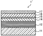
図1は、本発明の方法により製造されるEUVマスクブランクの1実施形態を示す概略断面図である。図1に示すEUVマスクブランク1は、基板11の成膜面上にEUV光を反射する反射層12、該反射層12を保護するための保護層14、および、EUV光を吸収する吸収層16がこの順に掲載されている。但し、本発明の方法により製造されるEUVマスクブランク1では、保護層14と、吸収層16と、の間にSi薄膜15が形成されている。なお、後述するが、Si薄膜15は、Si酸化薄膜、つまり、SiOx膜(0.1≦x≦2)であってもよい。
以下、EUVマスクブランク1の個々の構成要素について説明する。
The present invention will be described below with reference to the drawings.
FIG. 1 is a schematic cross-sectional view showing an embodiment of an EUV mask blank manufactured by the method of the present invention. An EUV mask blank 1 shown in FIG. 1 includes a
Hereinafter, individual components of the EUV mask blank 1 will be described.
基板11は、EUVマスクブランク用の基板としての特性を満たすことが要求される。
そのため、基板11は、低熱膨張係数(0±1.0×10⁻⁷/℃が好ましく、より好ましくは0±0.3×10-7/℃、さらに好ましくは0±0.2×10-7/℃、さらに好ましくは0±0.1×10-7/℃、特に好ましくは0±0.05×10-7/℃)を有し、平滑性、平坦度、およびマスクブランクまたはパターン形成後のフォトマスクの洗浄等に用いる洗浄液への耐性に優れたものが好ましい。基板11としては、具体的には低熱膨張係数を有するガラス、例えば、SiO2−TiO2系ガラス等を用いるが、これに限定されず、β石英固溶体を析出した結晶化ガラスや石英ガラスやシリコンや金属などの基板も使用できる。また、基板11上に応力補正膜のような膜を形成してもよい。
基板11は、0.15nm rms以下の平滑な表面と100nm以下の平坦度を有していることが、パターン形成後のフォトマスクにおいて高反射率および転写精度が得られるために好ましい。
基板11の大きさや厚さなどはマスクの設計値等により適宜決定される。後で示す実施例では、外形6インチ(152.4mm)角で、厚さ0.25インチ(6.3mm)のSiO2−TiO2系ガラスを用いた。
基板11の成膜面、つまり、反射層(多層反射膜)12が形成される側の表面には欠点が存在しないことが好ましい。しかし、存在している場合であっても、凹状欠点および/または凸状欠点によって位相欠点が生じないように、凹状欠点の深さおよび凸状欠点の高さが2nm以下であり、かつこれら凹状欠点および凸状欠点の半値幅は、60nm以下が好ましい。
The
Therefore, the
It is preferable that the
The size, thickness, etc. of the
It is preferable that no defects exist on the film-forming surface of the
EUVマスクブランクの反射層12に特に要求される特性は、高EUV光線反射率である。具体的には、EUV光の波長領域の光線を反射層12表面に入射角度6度で照射した際の、波長13.5nm付近の光線反射率の最大値は、60%以上が好ましく、63%以上がより好ましく、65%以上がさらに好ましい。また、反射層12の上に中間層13および保護層14を設けた場合であっても、波長13.5nm付近の光線反射率の最大値は、60%以上が好ましく、63%以上がより好ましく、65%以上がさらに好ましい。
A characteristic particularly required for the
EUVマスクブランクの反射層としては、EUV波長域において高反射率を達成できることから、高屈折率層と低屈折率層とを交互に複数回積層させた多層反射膜が広く用いられている。本発明のEUVマスクブランクでは、低屈折率層としてのMo層と、高屈折率層としてのSi層とを交互に複数回積層させたMo/Si多層反射膜を用いる。
Mo/Si多層反射膜の場合に、EUV光線反射率の最大値が60%以上の反射層12とするには、膜厚2.3±0.1nmのMo層と、膜厚4.5±0.1nmのSi層とを繰り返し単位数が30〜60になるように積層させればよい。
As a reflective layer of an EUV mask blank, since a high reflectance can be achieved in the EUV wavelength region, a multilayer reflective film in which a high refractive index layer and a low refractive index layer are alternately laminated a plurality of times is widely used. The EUV mask blank of the present invention uses a Mo / Si multilayer reflective film in which a Mo layer as a low refractive index layer and a Si layer as a high refractive index layer are alternately laminated a plurality of times.
In the case of a Mo / Si multilayer reflective film, in order to obtain the
なお、Mo/Si多層反射膜を構成する各層は、マグネトロンスパッタリング法、イオンビームスパッタリング法など、周知の成膜方法を用いて所望の厚さになるように成膜すればよい。例えば、イオンビームスパッタリング法を用いてMo/Si多層反射膜を形成する場合、ターゲットとしてMoターゲットを用い、スパッタリングガスとしてArガス(ガス圧1.3×10-2Pa〜2.7×10-2Pa)を使用して、イオン加速電圧300〜1500V、成膜速度0.03〜0.30nm/secで厚さ2.3nmとなるようにMo層を成膜し、次に、ターゲットとしてSiターゲットを用い、スパッタリングガスとしてArガス(ガス圧1.3×10-2Pa〜2.7×10-2Pa)を使用して、イオン加速電圧300〜1500V、成膜速度0.03〜0.30nm/secで厚さ4.5nmとなるようにSi層を成膜することが好ましい。これを1周期として、Mo層およびSi層を30〜60周期積層させることによりMo/Si多層反射膜が成膜される。 In addition, what is necessary is just to form each layer which comprises a Mo / Si multilayer reflective film so that it may become desired thickness using well-known film-forming methods, such as a magnetron sputtering method and an ion beam sputtering method. For example, when forming a Mo / Si multilayer reflective film using ion beam sputtering, a Mo target is used as a target, and Ar gas (gas pressure 1.3 × 10 −2 Pa to 2.7 × 10 − is used as a sputtering gas. 2 Pa), an Mo layer is formed to have a thickness of 2.3 nm at an ion acceleration voltage of 300 to 1500 V and a film formation rate of 0.03 to 0.30 nm / sec. using a target, using an Ar gas as a sputtering gas (gas pressure 1.3 × 10 -2 Pa~2.7 × 10 -2 Pa), an ion acceleration voltage 300 to 1,500 V, the deposition rate of 0.03 to 0 It is preferable to form the Si layer so that the thickness is 4.5 nm at 30 nm / sec. With this as one period, a Mo / Si multilayer reflective film is formed by laminating the Mo layer and the Si layer for 30 to 60 periods.
保護層14は、エッチングプロセス、具体的には、エッチングガスとして塩素系ガスを用いたドライエッチングプロセスにより吸収層16にパターン形成する際に、反射層12がエッチングプロセスによるダメージを受けないよう反射層12を保護する目的で設けられる。したがって保護層14の材質としては、吸収層16のエッチングプロセスによる影響を受けにくい、つまりこのエッチング速度が吸収層16よりも遅く、しかもこのエッチングプロセスによるダメージを受けにくい物質が選択される。
また、保護層14は、保護層14を形成した後であっても反射層12でのEUV光線反射率を損なうことがないように、保護層14自体もEUV光線反射率が高いことが好ましい。
本発明では、上記の条件を満足するため、保護層14として、Ru層、または、Ru化合物層が形成される。Ru化合物層としては、RuB、RuNb、および、RuZrからなる少なくとも1種で構成されることが好ましい。保護層14がRu化合物層である場合、Ruの含有率は50at%以上、80at%以上、特に90at%以上であることが好ましい。但し、保護層14がRuNb層の場合、保護層14中のNbの含有率が5〜40at%、特に5〜30at%が好ましい。
The
In addition, the
In the present invention, in order to satisfy the above conditions, a Ru layer or a Ru compound layer is formed as the
保護層14の厚さは、1〜10nmの範囲が、EUV光線反射率を高め、かつ耐エッチング特性を得られるという理由から好ましい。保護層14の厚さは、1〜5nmの範囲がより好ましく、2〜4nmの範囲がさらに好ましい。
The thickness of the
保護層14は、マグネトロンスパッタリング法、イオンビームスパッタリング法など周知の成膜方法を用いて成膜できる。
イオンビームスパッタリング法を用いて、保護層14としてRu層を形成する場合、ターゲットとしてRuターゲットを用い、アルゴン(Ar)雰囲気中で放電させればよい。
具体的には、以下の条件でイオンビームスパッタリングを実施すればよい。
スパッタリングガス:Ar(ガス圧1.3×10⁻²Pa〜2.7×10⁻²Pa)
イオン加速電圧:300〜1500V
成膜速度:0.03〜0.30nm/sec
The
When a Ru layer is formed as the
Specifically, ion beam sputtering may be performed under the following conditions.
Sputtering Gas: Ar (gas pressure 1.3 × 10 -2 Pa~2.7 × 10 -2 Pa)
Ion acceleration voltage: 300-1500V
Deposition rate: 0.03 to 0.30 nm / sec
本発明の方法により製造されるEUVマスクブランク1では、保護層14と、吸収層16と、の間に、膜厚2nm以下のSi薄膜が形成されている。なお、Si薄膜としては、Si酸化薄膜、つまりSiOx(0.1≦x≦2)であっても、同じ効果を奏する。そして、Si酸化薄膜を形成する場合、Si薄膜を形成後に、大気中に暴露することで形成してもよく、酸素雰囲気中でSi薄膜を形成してもよい。保護層14と、吸収層16と、の間にSi薄膜15を形成する理由は、以下のとおりである。
In the EUV mask blank 1 manufactured by the method of the present invention, a Si thin film having a thickness of 2 nm or less is formed between the
本発明において、保護層14上に形成されるSi薄膜15は、Siのとる構造として相対的に準安定であるアモルファス状態の熱安定性が高い。そのため、後述するように、少なくともTaおよびNを含有する吸収層について、TaとNとの組成比(Ta:N)が9:1〜3:7の広い範囲において、その結晶状態としてアモルファスの占める割合が高い構造を取りやすくなる。
In the present invention, the Si
但し、Si薄膜15の膜厚が大きくなると、EUVマスクブランクの特性、具体的には、EUV光照射時の吸収層の反射特性に影響を及ぼす。このため、Si薄膜15の膜厚は2nm以下にする必要がある。
Si薄膜15の膜厚は1nm以下が好ましく、0.8nm以下がより好ましく、0.5nm以下がさらに好ましい。
Si薄膜15は、膜厚が2nm以下である限り、膜厚の下限は限定されない。膜厚が小さい場合、保護層14全面を被覆できず、保護層14の表面の一部が露出した状態となる場合もあり得るが、このような場合であっても、Si薄膜15上に形成される吸収層16は、その結晶状態としてアモルファスの占める割合が高い構造を取りやすくなる。但し、この場合、Si薄膜15が形成されている表面上領域の疎密が偏らない状態において、保護層14表面に対する面積比で、Si薄膜またはSi酸化薄膜が25%以上被覆されていることが好ましく、50%以上被覆されていることがより好ましく、75%以上被覆されていることがさらに好ましい。つまり、Si薄膜の、平面視における膜の形状としては、例えば、島状の形状や網目状の形状の膜を含んでもよい。
However, when the film thickness of the Si
The film thickness of the Si
The lower limit of the film thickness of the Si
Si薄膜15は、マグネトロンスパッタリング法、イオンビームスパッタリング法など、周知の成膜方法を用いて所望の厚さになるように成膜すればよい。例えば、イオンビームスパッタリング法を用いてSi薄膜15を形成する場合、ターゲットとしてSiターゲットを用い、スパッタガスとしてArガス(ガス圧1.3×10⁻²Pa〜2.7×10⁻²Pa)を使用して、イオン加速電圧300〜1500V、成膜速度0.03〜0.30nm/secで厚さ2nm以下となるように成膜すればよい。
The Si
吸収層16に特に要求される特性は、EUV光線反射率が極めて低いことである。具体的には、EUV光の波長領域の光線を吸収層16表面に照射した際の、波長13.5nm付近の最大光線反射率は、0.5%以下が好ましく、0.1%以下がより好ましい。
上記の特性を達成するため、EUV光の吸収係数が高い材料で構成されることが好ましく、少なくともTaおよびNを含有する層であることが好ましい。
TaおよびNを含有する層としては、TaN、TaNH、TaBN、TaGaN、TaGeN、TaSiN、TaBSiN、および、PdTaNからなる群から選択されるいずれか1つを用いることが好ましい。これらの吸収層の好適組成の一例を挙げると以下のとおりである。
The characteristic particularly required for the
In order to achieve the above characteristics, the layer is preferably made of a material having a high EUV light absorption coefficient, and is preferably a layer containing at least Ta and N.
As the layer containing Ta and N, any one selected from the group consisting of TaN, TaNH, TaBN, TaGaN, TaGeN, TaSiN, TaBSiN, and PdTaN is preferably used. An example of a suitable composition of these absorption layers is as follows.
TaN層
Taの含有率:好ましくは30〜90at%、より好ましくは40〜80at%、さらに好ましくは40〜70at%、特に好ましくは50〜70at%
Nの含有率:好ましくは10〜70at%、より好ましくは20〜60at%、さらに好ましくは30〜60at%、特に好ましくは30〜50at%
TaN layer Ta content: preferably 30 to 90 at%, more preferably 40 to 80 at%, still more preferably 40 to 70 at%, particularly preferably 50 to 70 at%
N content: preferably 10 to 70 at%, more preferably 20 to 60 at%, still more preferably 30 to 60 at%, particularly preferably 30 to 50 at%
TaNH層
TaおよびNの合計含有率:好ましくは50〜99.9at%、より好ましくは90〜98at%、さらに好ましくは95〜98at%
Hの含有率:好ましくは0.1〜50at%、より好ましくは2〜10at%、さらに好ましくは2〜5at%
TaとNとの組成比(Ta:N):好ましくは9:1〜3:7、より好ましくは7:3〜4:6、さらに好ましくは7:3〜5:5
Total content of TaNH layer Ta and N: preferably 50 to 99.9 at%, more preferably 90 to 98 at%, still more preferably 95 to 98 at%
H content: preferably 0.1 to 50 at%, more preferably 2 to 10 at%, still more preferably 2 to 5 at%
Composition ratio of Ta and N (Ta: N): preferably 9: 1 to 3: 7, more preferably 7: 3 to 4: 6, still more preferably 7: 3 to 5: 5
TaBN層
TaおよびNの合計含有率:好ましくは75〜95at%、より好ましくは85〜95at%、さらに好ましくは90〜95at%
Bの含有率:好ましくは5〜25at%、より好ましくは5〜15at%、さらに好ましくは5〜10at%
TaとNとの組成比(Ta:N):好ましくは9:1〜3:7、より好ましくは7:3〜4:6、さらに好ましくは7:3〜5:5
Total content of TaBN layer Ta and N: preferably 75 to 95 at%, more preferably 85 to 95 at%, still more preferably 90 to 95 at%
B content: preferably 5 to 25 at%, more preferably 5 to 15 at%, still more preferably 5 to 10 at%
Composition ratio of Ta and N (Ta: N): preferably 9: 1 to 3: 7, more preferably 7: 3 to 4: 6, still more preferably 7: 3 to 5: 5
TaBSiN層
Bの含有率:1at%以上5at%未満、好ましくは1〜4.5at%、より好ましくは1.5〜4at%
Siの含有率:1〜25at%、好ましくは1〜20at%、より好ましくは2〜12at%
TaとNとの組成比(Ta:N):8:1〜1:1
Taの含有率:好ましくは50〜90at%、より好ましくは60〜80at%
Nの含有率:好ましくは5〜30at%、より好ましくは10〜25at%
Content of TaBSiN layer B: 1 at% or more and less than 5 at%, preferably 1 to 4.5 at%, more preferably 1.5 to 4 at%
Si content: 1 to 25 at%, preferably 1 to 20 at%, more preferably 2 to 12 at%
Composition ratio of Ta and N (Ta: N): 8: 1 to 1: 1
Ta content: preferably 50 to 90 at%, more preferably 60 to 80 at%
N content: preferably 5 to 30 at%, more preferably 10 to 25 at%
PdTaN層
TaおよびNの合計含有率:好ましくは30〜80at%、より好ましくは30〜75at%、さらに好ましくは30〜70at%
Pdの含有率:好ましくは20〜70at%、より好ましくは25〜70at%、さらに好ましくは30〜70at%
TaとNとの組成比(Ta:N):好ましくは1:7〜3:1、より好ましくは1:3〜3:1、さらに好ましくは3:5〜3:1
Total content of PdTaN layer Ta and N: preferably 30 to 80 at%, more preferably 30 to 75 at%, still more preferably 30 to 70 at%
Pd content: preferably 20 to 70 at%, more preferably 25 to 70 at%, still more preferably 30 to 70 at%
Composition ratio of Ta and N (Ta: N): preferably 1: 7 to 3: 1, more preferably 1: 3 to 3: 1, more preferably 3: 5 to 3: 1
本発明では、Si薄膜15を下地層として、上記組成の吸収層16、すなわち、少なくともTaおよびNを含有する層を形成するため、吸収層16の結晶状態として微結晶よりもアモルファスが占める割合が高い構造を取りやすくなり、表面の平滑性に優れる。
また、吸収層16表面の表面粗さは、0.5nm rms以下が好ましい。吸収層16表面の表面粗さが大きいと、吸収層16に形成されるパターンのエッジラフネスが大きくなり、パターンの寸法精度が低下する。パターンが微細になるに従いエッジラフネスの影響が顕著になるため、吸収層16表面は平滑であることが要求される。
吸収層16表面の表面粗さが0.5nm rms以下であれば、吸収層16表面が十分平滑であるため、エッジラフネスの影響によってパターンの寸法精度が悪化するおそれがない。また、吸収層16表面の表面粗さは、0.45nm rms以下がより好ましく、0.4nm rms以下がさらに好ましい。
In the present invention, since the
The surface roughness of the
If the surface roughness of the surface of the
吸収層16は、少なくともTaおよびNを含有する層であることにより、エッチングガスとして塩素系ガスを用いてドライエッチングを実施した際のエッチング速度が速く、保護層14とのエッチング選択比は10以上を示す。本明細書において、エッチング選択比は、下記式を用いて計算できる。
エッチング選択比
=(吸収層16のエッチング速度)/(保護層14のエッチング速度)
エッチング選択比は、10以上が好ましく、11以上がさらに好ましく、12以上が特に好ましい。
なお、保護層14と、吸収層16と、の間に存在するSi薄膜15は、エッチングガスとして塩素系ガスを用いてドライエッチングを実施した際のエッチング速度が速く、下記式で得られる、吸収層16と、Si薄膜15と、のエッチング選択比が1/2以下であり、また、Si薄膜15の膜厚は2nm以下ときわめて小さいため、吸収層16へのパターン形成時の影響は無視できる。
吸収層16と、Si薄膜15と、のエッチング選択比
=(吸収層16のエッチング速度)/(Si薄膜15のエッチング速度)
Since the
Etching selectivity = (etching rate of absorbing layer 16) / (etching rate of protective layer 14)
The etching selectivity is preferably 10 or more, more preferably 11 or more, and particularly preferably 12 or more.
The Si
Etching selectivity between
また、吸収層16の厚さは、50〜100nmの範囲が好ましい。本発明における吸収層16は、マグネトロンスパッタリング法やイオンビームスパッタリング法のようなスパッタリング法などの成膜方法を用いて形成できる。
The thickness of the
また、本発明の方法により製造されるEUVマスクブランクは、図2に示すEUVマスクブランク10のように、反射層12と、保護層14と、の間に、SiおよびNを含有する中間層13を形成してもよい。本願出願人が、特許文献4で提案するように、EUV光線反射率低下の要因が、多層反射膜の最上層のSi層から保護層へのSiの拡散によりEUVマスクブランクの上部からの酸化が促進されることによるもの、つまり、Mo/Si多層反射膜よりも上側の膜からの酸化によるものが主であり、酸化によるEUV光線反射率低下を防止するためには、Mo/Si多層反射膜の上の層、つまり保護層からの酸化を防止すれば十分である。この構成とすることで、保護層14からの酸化によるEUV光線反射率の低下を抑制できる。
Moreover, the EUV mask blank manufactured by the method of the present invention has an
本発明の方法により製造されるEUVマスクブランク10では、反射層12と、保護層14と、の間に、SiおよびNを含有する中間層13が形成されることによって、保護層14からの酸化によるEUV光線反射率の低下を抑制できる。このように、SiおよびNを含有する中間層13が形成されることによって、保護層14からの酸化によるEUV光線反射率の低下が抑制される理由は以下によると考えられる。
In the EUV mask blank 10 manufactured by the method of the present invention, an
中間層13は、SiおよびNを含有することで、成膜後のEUV光線反射率が高く、かつ酸化を抑制する効果を有すると考えられる。これにより、EUVマスクブランク製造時に実施される工程や該EUVマスクブランクからフォトマスクを製造する際に実施される工程(例えば、洗浄、欠陥検査、加熱工程、ドライエッチング、欠陥修正の各工程)において、あるいは該EUV露光時において、保護層14が酸化されるような状況が生じた場合でも、酸化を抑制する効果を有する中間層13が存在することによって、EUV光線反射率の低下が抑制できると考えられる。つまり、該中間層13の下にあるMo/Si多層反射膜が酸化されること、より具体的には、Mo/Si多層反射膜の最上層のSi層が酸化されることが抑制でき、その結果、保護層14からの酸化によるEUV光線反射率の低下が抑制できると考えられる。
なお、反射層12(Mo/Si多層反射膜)と、保護層14と、の間に中間層13が形成されていることによって、保護層14の形成時にMo/Si多層反射膜の最上層であるSi層中のSiが保護層14中に拡散することも抑制できる。
It is considered that the
In addition, since the
中間層13は、Siを75〜99.5at%、Nを0.5〜25at%含有することが好ましい。
中間層13におけるNの含有率が0.5at%未満の場合、上述した更なる酸化を抑制する効果が不十分となり、保護層14からの酸化によるEUV光線反射率の低下を抑制する効果が不十分となるおそれがある。
詳しくは後述するが、SiおよびNを含有する中間層13は、Mo/Si多層反射膜を形成した後、該Mo/Si多層反射膜の最上層であるSi層表面を、大気中へ暴露することなく、窒素含有雰囲気に暴露することによって形成できるが、中間層13におけるNの含有率が25at%超の場合、Mo/Si多層反射膜の最上層であるSi層の成膜時、または、中間層13上に形成される保護層14の成膜時のいずれか、あるいはそれらの両方の成膜時において、成膜する雰囲気中にNが存在していたものと考えられる。Nが存在する雰囲気での成膜は成膜中の欠点が増加するおそれがある。
The
When the N content in the
As will be described in detail later, the
中間層13はSiを85〜99.5at%含有し、Nを0.5〜15at%含有することがより好ましく、Siを90〜99.5at%含有し、Nを0.5〜10at%含有することがさらに好ましく、Siを91〜99at%含有し、Nを1〜9at%含有することがさらに好ましく、Siを91〜97at%含有し、Nを3〜9at%含有することがさらに好ましく、Siを92〜95at%含有し、Nを5〜8at%含有することが特に好ましい。
The
また、中間層13は、中間層13中のSiが侵食されるおそれがあるため、F(フッ素)を含まないことが好ましい。さらに、中間層13は、該中間層13中にC(炭素)やH(水素)が含まれていると、該中間層13中のO(酸素)と反応して、該中間層13中のOが放出され該中間層13の構造が劣化するおそれがあるため、CやHを含まないことが好ましい。これらの理由から、中間層13におけるF、CおよびHの含有率はそれぞれ3at%以下が好ましく、1at%以下がより好ましい。また、中間層13は、該中間層13に、Ni、Y、Ti、La、CrまたはRhといった元素が含まれていると、EUVマスクブランクをエッチングした場合に、エッチングレートの違いによる表面粗さの増加のおそれがあるため、これらを含まないことが好ましい。この理由から、中間層13におけるNi、Y、Ti、La、CrおよびRhの含有率はそれぞれ3at%以下が好ましく、1at%以下がより好ましい。
また、中間層13におけるOの含有率も、3at%以下が好ましく、1at%以下がより好ましい。
The
Further, the O content in the
中間層13の膜厚は0.2〜2.5nmの範囲が、保護層14からの酸化によるEUV光線反射率の低下を抑制する効果という点から好ましく、0.4〜2nmの範囲がより好ましく、0.5〜1.5nmの範囲がさらに好ましい。また、多層反射膜の最上層のSi層の膜厚は、該Si膜表面を窒素含有雰囲気に暴露することによって中間層13を形成するため、2〜4.8nmの範囲、特に2.5〜4nmの範囲が好ましい。
The thickness of the
SiおよびNを含有する中間層13は、Mo/Si多層反射膜の形成後、該Mo/Si多層反射膜の最上層であるSi層表面を、大気中へ暴露することなく、窒素含有雰囲気に暴露することで該Si層表面を軽微に窒化させることにより、すなわち、Si層表面にNを含有させることによって形成できる。なお、本明細書における窒素含有雰囲気とは、窒素ガス雰囲気または、窒素ガスとアルゴン等の不活性ガスとの混合ガス雰囲気を意味する。該混合ガス雰囲気の場合、雰囲気中の窒素ガス濃度は、20vol%以上が好ましく、50vol%以上がより好ましく、80vol%以上がさらに好ましい。
ここで、Mo/Si多層反射膜の形成後、該Mo/Si多層反射膜の最上層であるSi層表面を、大気中へ暴露することなく、窒素含有雰囲気に暴露するのは、窒素雰囲気に暴露する前に、該Si層表面を大気中に暴露すると、該Si層表面が酸化されてしまうおそれがある。その場合、その後、窒素雰囲気に暴露しても該Si層表面の窒化により、該Si層表面にNを含有させることができず、SiおよびNを含有する中間層13が形成できないおそれがある。
The
Here, after the formation of the Mo / Si multilayer reflective film, the surface of the Si layer, which is the uppermost layer of the Mo / Si multilayer reflective film, is exposed to a nitrogen-containing atmosphere without being exposed to the atmosphere. If the surface of the Si layer is exposed to the atmosphere before exposure, the surface of the Si layer may be oxidized. In that case, even if it is exposed to a nitrogen atmosphere after that, the Si layer surface cannot be made to contain N due to nitriding of the Si layer surface, and there is a possibility that the
Si層表面を暴露する窒素含有雰囲気は、窒素分圧(Torr)と暴露時間(s)の積として、1×10⁻⁶Torr・s(=1L(Langmuir))以上が好ましい。窒素分圧をPa表記で表す場合、窒素含有雰囲気の窒素分圧(Pa)と暴露時間(s)の積として、1.33×10⁻⁴Pa・s以上が好ましいことになる。
窒素分圧と暴露時間との積は、窒素含有雰囲気中の窒素がSi層表面に衝突する頻度を示す指標であり、以下、本明細書において、「窒素の暴露量」という場合もある。この値は、1×10⁻⁶Torr・s以上(1.33×10⁻⁴Pa・s以上)が、Si層表面の窒化により、SiおよびNを含有する中間層13を形成するうえで好ましく、1×10⁻³Torr・s以上(1.33×10⁻¹Pa・s以上)がより好ましく、1×10⁻²Torr・s以上(1.33Pa・s以上)がさらに好ましく、1×10⁻¹Torr・s以上(13.3Pa・s以上)が特に好ましい。
なお、Si層表面を暴露する窒素含有雰囲気における窒素分圧は、1×10⁻⁴Torr〜820Torr(1.33×10⁻²Pa〜109.32kPa)が好ましい。
ここで、窒素含有雰囲気が窒素ガス雰囲気の場合、上記の窒素分圧は該窒素ガス雰囲気の雰囲気圧力を指す。
The nitrogen-containing atmosphere that exposes the Si layer surface is preferably 1 × 10 −6 Torr · s (= 1 L (Langmuir)) or more as the product of the nitrogen partial pressure (Torr) and the exposure time (s). When the nitrogen partial pressure is expressed in Pa, the product of the nitrogen partial pressure (Pa) and the exposure time (s) in the nitrogen-containing atmosphere is preferably 1.33 × 10 −4 Pa · s or more.
The product of the nitrogen partial pressure and the exposure time is an index indicating the frequency with which nitrogen in the nitrogen-containing atmosphere collides with the surface of the Si layer, and may hereinafter be referred to as “nitrogen exposure amount”. This value is preferably 1 × 10 −6 Torr · s or more (1.33 × 10 −4 Pa · s or more) in order to form the
The nitrogen partial pressure in the nitrogen-containing atmosphere that exposes the Si layer surface is preferably 1 × 10 −4 Torr to 820 Torr (1.33 × 10 −2 Pa to 109.32 kPa).
Here, when the nitrogen-containing atmosphere is a nitrogen gas atmosphere, the nitrogen partial pressure indicates the atmospheric pressure of the nitrogen gas atmosphere.
Si層表面の酸化を防止するためには、Si層表面を暴露する窒素含有雰囲気における酸素濃度がきわめて低いことが好ましい。具体的には、窒素含有雰囲気における窒素分圧が上記範囲の場合、すなわち、窒素含有雰囲気における窒素分圧が1×10⁻⁴Torr〜820Torr(1.33×10⁻²Pa〜109.32kPa)の場合、雰囲気中の酸素分圧が1×10⁻⁶Torr(1.33×10⁻⁴Pa)以下が好ましい。
また、Si層表面の酸化を防止するためには、Si層表面を暴露する窒素含有雰囲気におけるO3、H2OおよびOHの濃度もきわめて低いことが好ましい。具体的には、窒素含有雰囲気における窒素分圧が上記範囲の場合、すなわち、窒素含有雰囲気における窒素分圧が1×10⁻⁴Torr〜820Torr(1.33×10⁻²Pa〜109.32kPa)の場合、雰囲気中のO3、H2OおよびOHの分圧は、それぞれ1×10⁻⁶Torr(1.33×10⁻⁴Pa)以下が好ましい。
また、Si層を侵食するおそれがあるので、窒素含有雰囲気におけるF2の濃度もきわめて低いことが好ましい。具体的には、窒素含有雰囲気における窒素分圧が上記範囲の場合、すなわち、窒素含有雰囲気における窒素分圧が1×10⁻⁴Torr〜820Torr(1.33×10⁻²Pa〜109.32kPa)の場合、雰囲気中のF2の分圧は、1×10⁻⁶Torr以下が好ましい。
In order to prevent oxidation of the Si layer surface, it is preferable that the oxygen concentration in the nitrogen-containing atmosphere that exposes the Si layer surface is extremely low. Specifically, when the nitrogen partial pressure in the nitrogen-containing atmosphere is in the above range, that is, the nitrogen partial pressure in the nitrogen-containing atmosphere is 1 × 10 −4 Torr to 820 Torr (1.33 × 10 −2 Pa to 109.32 kPa). In this case, the oxygen partial pressure in the atmosphere is preferably 1 × 10 −6 Torr (1.33 × 10 −4 Pa) or less.
In order to prevent oxidation of the Si layer surface, it is preferable that the O 3 , H 2 O, and OH concentrations in the nitrogen-containing atmosphere that exposes the Si layer surface are also extremely low. Specifically, when the nitrogen partial pressure in the nitrogen-containing atmosphere is in the above range, that is, the nitrogen partial pressure in the nitrogen-containing atmosphere is 1 × 10 −4 Torr to 820 Torr (1.33 × 10 −2 Pa to 109.32 kPa). In this case, the partial pressures of O 3 , H 2 O and OH in the atmosphere are each preferably 1 × 10 −6 Torr (1.33 × 10 −4 Pa) or less.
Further, since there is a possibility of eroding the Si layer, it is preferable that the concentration of F 2 in the nitrogen-containing atmosphere is also extremely low. Specifically, when the nitrogen partial pressure in the nitrogen-containing atmosphere is in the above range, that is, the nitrogen partial pressure in the nitrogen-containing atmosphere is 1 × 10 −4 Torr to 820 Torr (1.33 × 10 −2 Pa to 109.32 kPa). In this case, the partial pressure of F 2 in the atmosphere is preferably 1 × 10 −6 Torr or less.
また、Si層表面を暴露する窒素含有雰囲気の温度は、0〜170℃が好ましい。窒素含有雰囲気の温度が0℃未満だと、真空中の残留水分の吸着による影響の問題が生じるおそれがある。窒素含有雰囲気の温度が170℃超だと、Si層の窒化が過度に進行して、Mo/Si多層反射膜のEUV光線反射率の低下が生じるおそれがある。
窒素含有雰囲気の温度は10〜160℃がより好ましく、20〜150℃がさらに好ましい。
なお、後述するように、Si層表面を窒素含有雰囲気に暴露する際に、該Si層表面を上記の温度範囲で熱処理してもよい。
また、Mo/Si多層反射膜の最上層であるSi層表面を窒素含有雰囲気に暴露して該Si層表面を軽微に窒化させることにより、すなわち、Si層表面に窒素を含有させることによって、中間膜13を形成することで、保護層14形成後のEUV光線反射率の低下が抑制され、酸化耐久性が向上するので好ましい。
The temperature of the nitrogen-containing atmosphere that exposes the surface of the Si layer is preferably 0 to 170 ° C. If the temperature of the nitrogen-containing atmosphere is less than 0 ° C., there may be a problem of influence due to adsorption of residual moisture in vacuum. If the temperature of the nitrogen-containing atmosphere exceeds 170 ° C., the nitridation of the Si layer proceeds excessively, and the EUV light reflectance of the Mo / Si multilayer reflective film may be lowered.
The temperature of the nitrogen-containing atmosphere is more preferably 10 to 160 ° C, further preferably 20 to 150 ° C.
As will be described later, when the surface of the Si layer is exposed to a nitrogen-containing atmosphere, the surface of the Si layer may be heat-treated in the above temperature range.
Further, by exposing the surface of the Si layer, which is the uppermost layer of the Mo / Si multilayer reflective film, to a nitrogen-containing atmosphere to lightly nitride the surface of the Si layer, that is, by adding nitrogen to the surface of the Si layer, intermediate Forming the
後述する実施例1では、Si層表面を窒素含有雰囲気に暴露する時間を600secとしているが、Si層表面を窒素含有雰囲気に暴露する時間はこれに限定されず、上述した窒素含有雰囲気に関する条件を満たす範囲で適宜選択できる。 In Example 1 described later, the time for exposing the surface of the Si layer to the nitrogen-containing atmosphere is 600 seconds, but the time for exposing the surface of the Si layer to the nitrogen-containing atmosphere is not limited to this, and the conditions regarding the nitrogen-containing atmosphere described above are used. It can be selected as appropriate within the range to satisfy.
さらに、Mo/Si多層反射膜を形成した後、該Mo/Si多層反射膜の最上層であるSi層表面を、大気中へ暴露することなく、窒素含有雰囲気に暴露する際に、該窒素含有雰囲気で熱処理することによって中間層13を形成してもよい。Mo/Si多層反射膜の最上層であるSi層表面を窒素雰囲気に暴露する際に、該Si層表面を熱処理することによって、該Si層表面の窒化、すなわち、該Si層表面へのNの含有が促進される。
なお、Mo/Si多層反射膜を形成した後、該Mo/Si多層反射膜の最上層であるSi層表面を、大気中へ暴露することなく、窒素含有雰囲気で熱処理するには、Si層の形成後、Mo/Si多層反射膜が形成された基板を、Si層を形成した成膜チャンバ内、または、該成膜チャンバに隣接するチャンバ内に保持した状態で、チャンバ中のガスを窒素ガス(または窒素ガスとアルゴン等の不活性ガスとの混合ガス)に置換し、その置換したガス中でSi層を熱処理すればよい。
Si層表面を窒素含有雰囲気中で熱処理する際の熱処理温度は、120〜160℃、特に130〜150℃が好ましい。
Further, after forming the Mo / Si multilayer reflective film, the surface of the Si layer, which is the uppermost layer of the Mo / Si multilayer reflective film, is exposed to a nitrogen-containing atmosphere without being exposed to the atmosphere. The
In addition, after forming the Mo / Si multilayer reflective film, in order to heat-treat the surface of the Si layer, which is the uppermost layer of the Mo / Si multilayer reflective film, in a nitrogen-containing atmosphere without exposing it to the atmosphere, After the formation, the substrate in which the Mo / Si multilayer reflective film is formed is held in the deposition chamber in which the Si layer is formed or in a chamber adjacent to the deposition chamber, and the gas in the chamber is replaced with nitrogen gas. (Or a mixed gas of nitrogen gas and inert gas such as argon) and the Si layer may be heat-treated in the substituted gas.
The heat treatment temperature when the Si layer surface is heat-treated in a nitrogen-containing atmosphere is preferably 120 to 160 ° C, particularly preferably 130 to 150 ° C.
実施例1に示す手順のように、減圧雰囲気下でSi層表面を窒素ガス、または、窒素ガスとアルゴン等の不活性ガスとの混合ガスに暴露する手順は、Mo/Si多層反射膜の成膜と、保護層の成膜と、を同一のチャンバを用いて実施する場合に、Si層表面を窒素ガス(または窒素ガスとアルゴン等の不活性ガスとの混合ガス)に暴露する手順の実施後、保護層の成膜を実施する前にチャンバ内の窒素ガス(または窒素ガスとアルゴン等の不活性ガスとの混合ガス)を排気することが重要である点を考慮することが好ましい手順である。また、この手順は、Si層表面への窒素ガス(または窒素ガスとアルゴン等の不活性ガスとの混合ガス)の暴露量を制御することによって、中間層13のN含有量を制御できるという点でも好ましい手順である。
The procedure of exposing the surface of the Si layer to nitrogen gas or a mixed gas of nitrogen gas and an inert gas such as argon under a reduced pressure atmosphere as in the procedure shown in Example 1 is the formation of a Mo / Si multilayer reflective film. Implementation of procedures for exposing the Si layer surface to nitrogen gas (or a mixed gas of nitrogen gas and an inert gas such as argon) when the film and the protective layer are formed in the same chamber After that, it is preferable to consider that it is important to exhaust the nitrogen gas (or a mixed gas of nitrogen gas and an inert gas such as argon) in the chamber before forming the protective layer. is there. Further, this procedure can control the N content of the
Mo/Si多層反射膜を形成した後、該Mo/Si多層反射膜の最上層であるSi層表面を、大気中へ暴露することなく、窒素含有雰囲気に暴露する際に、該窒素含有雰囲気で熱処理することによって、該Si層表面の窒化、すなわち、該Si層表面へのNの含有を促進できることを上述したが、これに限らない。この他に、減圧雰囲気下でSi層表面を窒素ガス、または、窒素ガスとアルゴン等の不活性ガスとの混合ガスに暴露する場合、該減圧雰囲気をプラズマ状態に保持することも、Si層表面の窒化、すなわち、Si層表面の窒素含有、を促進するうえで好ましい。
但し、この場合でも、プラズマ状態でイオン化した窒素ガス(または窒素ガスとアルゴン等の不活性ガスとの混合ガス)に電圧を印加してSi層表面にイオン照射すると、イオン化した窒素が加速された状態でSi層表面に衝突するため、Si層の窒化が過度に進行してMo/Si多層反射膜のEUV光線反射率の低下が生じるおそれがあるため、プラズマ状態でイオン化した窒素ガス(または窒素ガスとアルゴン等の不活性ガスとの混合ガス)に電圧を印加しないこと、つまり、イオン照射をしないことが中間層13の窒素量を適量に制御できる点で特に好ましい。
また、減圧雰囲気下でSi層表面を窒素ガス、または、窒素ガスとアルゴン等の不活性ガスとの混合ガスに暴露する場合、該減圧雰囲気中でSi層表面に紫外線を照射することもSi層表面の窒化、すなわち、Si層表面のN含有、を促進するうえで好ましい。
After forming the Mo / Si multilayer reflective film, when the surface of the Si layer, which is the uppermost layer of the Mo / Si multilayer reflective film, is exposed to a nitrogen-containing atmosphere without being exposed to the atmosphere, Although it has been described above that nitriding of the surface of the Si layer, that is, inclusion of N in the surface of the Si layer can be promoted by heat treatment, the present invention is not limited thereto. In addition, when the surface of the Si layer is exposed to nitrogen gas or a mixed gas of nitrogen gas and an inert gas such as argon under a reduced pressure atmosphere, the reduced pressure atmosphere may be maintained in a plasma state. This is preferable for promoting nitriding of the silicon layer, that is, containing nitrogen on the surface of the Si layer.
However, even in this case, when a voltage is applied to nitrogen gas ionized in a plasma state (or a mixed gas of nitrogen gas and an inert gas such as argon) and ion irradiation is performed on the surface of the Si layer, the ionized nitrogen is accelerated. Since it collides with the surface of the Si layer in a state, the nitridation of the Si layer may proceed excessively and the EUV light reflectance of the Mo / Si multilayer reflective film may be reduced, so that the ionized nitrogen gas (or nitrogen) It is particularly preferable that no voltage is applied to the gas (a mixed gas of a gas and an inert gas such as argon), that is, that the amount of nitrogen in the
In addition, when the Si layer surface is exposed to nitrogen gas or a mixed gas of nitrogen gas and an inert gas such as argon in a reduced pressure atmosphere, the Si layer surface may be irradiated with ultraviolet rays in the reduced pressure atmosphere. It is preferable for promoting surface nitriding, that is, N content on the surface of the Si layer.
なお、保護層14には、隣接する中間層13から若干ではあるがNが拡散する。中間層13から拡散したNの保護層14中の含有率は0.1〜10at%が好ましく、0.1〜5at%がより好ましい。
中間層13から拡散したNは、中間層13からの距離が増加するにつれて保護層14中の含有率が減少していく組成、つまり、中間層13との界面付近のN含有率が高く、Si薄膜15との界面付近の含有率が低くなるように、保護層14中のN含有率が傾斜する組成であってもよい。
In the
N diffused from the
また、保護層14には、隣接する中間層13から若干ではあるがSiが拡散する可能性がある。中間層13から拡散したSiを保護層14が含有する場合、保護層14中のSiの含有率は、0.1〜4.5at%が好ましく、0.1〜4at%がより好ましい。なお、隣接する中間層13からSiやNが保護層14中に若干拡散しても、保護層14の特性はほとんど悪化しない。
Further, Si may diffuse slightly from the adjacent
さらに、本発明の方法により製造されるEUVマスクブランクは、図3に示すEUVマスクブランク20のように、反射層12と、保護層14と、の間に、窒素およびSiを後述する所定の量含有する第1層21、および、Ru、窒素およびSiを後述する所定の量含有する第2層22の二層構造からなる中間層13が形成されていてもよい。
Furthermore, the EUV mask blank manufactured by the method of the present invention has a predetermined amount of nitrogen and Si described later between the
本発明の方法により製造されるEUVマスクブランク20は、反射層12と、保護層14と、の間に、窒素を0.5〜25at%含有し、Siを75〜99.5at%含有する第1層21、および、Ruを60〜99.8at%含有し、窒素を0.1〜10at%含有し、Siを0.1〜30at%含有する第2層22からなる二層構造の中間層13を形成することによって、Ru保護層の酸化によるEUV光線反射率の低下を抑制する。反射層12と、保護層14と、の間に、上記した組成の二層構造(第1層21,第2層22)の中間層13を形成することによって、Ru保護層の酸化によるEUV光線反射率の低下が抑制される理由は以下によると考えられる。
上記二層構造の中間層13は、第1層21がSi膜中に窒素を多量に含むことによる反射率の低下が無い程度に窒素を含有することによって、成膜後の反射率が高く、かつ酸化を抑制する効果を有すると考えられる。
そして、第2層22が、Ruに加えて、微量の窒素を含有することにより、Ru保護層が酸化されるような状況が生じた場合でも、第2層よりも下にある層構造の酸化を抑制することができる。これにより、マスクブランク製造時に実施される工程や該マスクブランクからフォトマスクを製造する際に実施される工程(例えば、洗浄、欠陥検査、加熱工程、ドライエッチング、欠陥修正の各工程)において、あるいは該EUV露光時において、Ru保護層が酸化されるような状況が生じた場合でも、酸化を抑制する効果を有する中間層13が存在することによって、該中間層13の下にあるMo/Si多層反射膜が酸化されること、より具体的には、Mo/Si多層反射膜の最上層のSi膜が酸化されることが抑制されると考えられ、その結果、Ru保護層の酸化によるEUV光線反射率の低下が抑制されると考えられる。
また、反射層12(Mo/Si多層反射膜)と、保護層14(Ru保護層)と、の間に上記二層構造の中間層13が存在することにより、保護層14の形成時にMo/Si多層反射膜の最上層であるSi膜中のSiがRu保護層中に拡散することを抑制できる。
The EUV mask blank 20 produced by the method of the present invention contains 0.5 to 25 at% nitrogen and 75 to 99.5 at% Si between the
The
Even when the
Further, since the
第1層21における窒素の含有率が0.5at%未満の場合、上述した更なる酸化を抑制する効果が不十分となり、Ru保護層の酸化によるEUV光線反射率の低下を抑制する効果が不十分となる。
詳しくは後述するが、上記した二層構造の中間層13は、Mo/Si多層反射膜を形成した後、Mo/Si多層反射膜の最上層であるSi膜表面を窒素含有雰囲気に暴露することによって形成できるが、第1層21における窒素の含有率が25at%超の場合、Mo/Si多層反射膜の最上層であるSi膜の成膜時、または、中間層13上に形成される保護層14の成膜時のいずれか、あるいはそれらの両方の成膜時に窒素が添加されていたものと考えられるが、窒素を添加した成膜は成膜中の欠点が増加し問題が生じる。
第1層21は窒素を0.5〜15at%含有し、Siを85〜99.5at%含有することが好ましく、窒素を0.5〜10at%含有し、Siを90〜99.5at%含有することがより好ましく、窒素を1〜9at%含有し、Siを91〜99at%含有することがさらに好ましく、窒素を3〜9at%含有し、Siを91〜97at%含有することがさらに好ましく、窒素を5〜8at%含有し、Siを92〜95at%含有することが特に好ましい。
When the nitrogen content in the
As will be described in detail later, the
The
第2層22におけるRuの含有率が60at%未満の場合、Ru保護層の酸化によるEUV光線反射率の低下のおそれがある。一方、第2層22におけるRuの含有率が98.5at%超の場合、上述した微量の窒素を含有することによる効果が発揮されにくくなる。
第2層22における窒素の含有率が0.1at%未満の場合、上述した微量の窒素を含有することによる効果が発揮されにくくなる。一方、第2層22における窒素の含有率が10at%超の場合、Ru保護層の過剰な窒化によるEUV光線反射率の低下のおそれがある。
第2層22におけるSiの含有率が0.1at%未満の場合、第1層21との密着性に劣るおそれがある。一方、第2層22におけるSiの含有率が30at%超の場合、Ru保護層の酸化によるEUV光線反射率の低下のおそれがある。
第2層22はRuを60〜99.8at%含有し、窒素を0.1〜10at%含有し、Siを0.1〜30at%含有することが好ましく、Ruを75〜99.8at%含有し、窒素を0.1〜5at%含有し、Siを0.1〜20at%含有することがより好ましく、Ruを90〜99.8at%含有し、窒素を0.1〜2.5at%含有し、Siを0.1〜7.5at%含有することがさらに好ましい。
When the content ratio of Ru in the
When the content rate of nitrogen in the
When the Si content in the
The
中間層13を構成する第1層21および第2層22中のSiが侵食されるおそれがあるため、中間層13を構成する各層(第1層21および第2層22)はフッ素を含まないことが好ましい。また、中間層13を構成する各層(第1層21および第2層22)に炭素や水素が含まれていると、中間層13を構成する各層(第1層21および第2層22)に含まれる酸素と反応して、層中の酸素が放出されるおそれがあるため、中間層13を構成する各層(第1層21および第2層22)は炭素や水素を含まないことが好ましい。これらの理由から、中間層13を構成する各層(第1層21および第2層22)におけるフッ素、炭素および水素の含有率はそれぞれ3at%以下が好ましく、1at%以下がより好ましい。また、同様に、中間層13を構成する各層(第1層21および第2層22)におけるNi、Y、Ti、La、CrまたはRhといった元素含有率は3at%以下が好ましく、1at%以下がより好ましい。
Since Si in the
中間層13を構成する第1層21および第2層22の合計膜厚が0.2〜2.5nmであると、Ru保護層の酸化によるEUV光線反射率の低下を抑制する効果という点から好ましく、0.4〜2nmがより好ましく、0.5〜1.5nmがさらに好ましい。
また、多層反射膜の最上層のSi層の膜厚は、窒素含有雰囲気に暴露して上記二層構造の中間層13を形成するため、2〜4.8nm、特に2.5〜4nmが好ましい。
When the total film thickness of the
The thickness of the uppermost Si layer of the multilayer reflective film is preferably 2 to 4.8 nm, particularly preferably 2.5 to 4 nm, because the
第1層21の膜厚が0.1〜2.4nmであると、Ru保護層の酸化によるEUV光線反射率の低下を抑制する効果という点から好ましく、0.4〜1.5nmがより好ましく、0.8〜1.3nmがさらに好ましい。
When the film thickness of the
第2層22の膜厚が0.1〜2.4nmであると、Ru保護層の酸化によるEUV光線反射率の低下を抑制する効果という点から好ましく、0.4〜1.5nmがより好ましく、0.8〜1.2nmがさらに好ましい。
When the thickness of the
中間層13を構成する各層(第1層21、第2層22)のうち、第1層21の膜厚が小さいことが、過剰なSiN層の窒化によるEUV光線反射率の低下を抑制する理由から好ましい。
第2層22と第1層21との膜厚の差(第2層22の膜厚−第1層21の膜厚)は、0〜2.3nmが好ましく、0〜1.1nmがより好ましく、0〜0.4nmがさらに好ましい。
The reason why the thickness of the
The difference in film thickness between the
上記二層構造の中間層13は、Mo/Si多層反射膜の形成後、該Mo/Si多層反射膜の最上層であるSi膜表面を窒素含有雰囲気に暴露することで該Si膜表面を軽微に窒化させることによって形成できる。
The
Si膜表面を暴露する窒素含有雰囲気は、窒素分圧(Torr)と暴露時間(s)の積が1×10⁻⁶Torr・s(=1L(Langmuir))以上であることが好ましい。この値は、1×10⁻⁶Torr・s以上が、Si膜表面の窒化により上記した二層構造の中間層13を形成するうえで好ましく、1×10⁻³Torr・s以上がより好ましく、1×10⁻²Torr・s以上がさらに好ましく、1×10⁻¹Torr・s以上がさらに好ましい。
The nitrogen-containing atmosphere for exposing the Si film surface preferably has a product of nitrogen partial pressure (Torr) and exposure time (s) of 1 × 10 −6 Torr · s (= 1 L (Langmuir)) or more. This value is preferably 1 × 10 −6 Torr · s or more, more preferably 1 × 10 −3 Torr · s or more when forming the
Si膜表面を暴露する窒素含有雰囲気が上記の条件を満たす限り、Si膜表面を窒素含有雰囲気に暴露する手順は特に限定されない。但し、減圧雰囲気下でSi膜表面を窒素ガス、または、窒素ガスとアルゴン等の不活性ガスとの混合ガスに暴露する手順は、多層反射膜の成膜と、保護層の成膜と、を同一のチャンバを用いて実施する場合に、Si膜表面を窒素ガス(または窒素ガスとアルゴン等の不活性ガスとの混合ガス)に暴露する手順の実施後、保護層の成膜を実施する前にチャンバ内の窒素ガス(または窒素ガスとアルゴン等の不活性ガスとの混合ガス)を排気することが必要である点を考慮することが好ましい手順である。また、この手順は、Si膜表面への窒素ガス(または窒素ガスとアルゴン等の不活性ガスとの混合ガス)の暴露量を制御することによって、中間層13を構成する各層(第1層21、第2層22)における窒素含有量を制御できるという点でも好ましい手順である。
なお、減圧雰囲気下でSi膜表面を窒素ガス、または、窒素ガスとアルゴン等の不活性ガスとの混合ガスに暴露する場合、該減圧雰囲気をプラズマ状態に保持することがSi膜表面の窒化を促進するうえで好ましい。この場合でも、プラズマ状態でイオン化した窒素ガス(または窒素ガスとアルゴン等の不活性ガスとの混合ガス)に電圧を印加してSi膜表面にイオン照射すると、イオン化した窒素が加速された状態でSi膜表面に衝突するため、Si膜の窒化が過度に進行してMo/Si多層反射膜のEUV光線反射率の低下が生じるおそれがあるため、プラズマ状態でイオン化した窒素ガス(または窒素ガスとアルゴン等の不活性ガスとの混合ガス)に電圧を印加しないこと、つまり、イオン照射をしないことが中間層13を構成する各層(第1層21、第2層22)における窒素含有量を適量に制御できる点で特に好ましい。
As long as the nitrogen-containing atmosphere that exposes the Si film surface satisfies the above conditions, the procedure for exposing the Si film surface to the nitrogen-containing atmosphere is not particularly limited. However, the procedure of exposing the surface of the Si film to nitrogen gas or a mixed gas of nitrogen gas and an inert gas such as argon under a reduced-pressure atmosphere includes the formation of a multilayer reflective film and the formation of a protective layer. When performing using the same chamber, after performing the procedure of exposing the surface of the Si film to nitrogen gas (or a mixed gas of nitrogen gas and an inert gas such as argon), before forming the protective layer It is a preferable procedure to take into account that it is necessary to exhaust the nitrogen gas in the chamber (or a mixed gas of nitrogen gas and an inert gas such as argon). Further, this procedure controls each layer (first layer 21) constituting the
When the surface of the Si film is exposed to nitrogen gas or a mixed gas of nitrogen gas and an inert gas such as argon under a reduced pressure atmosphere, maintaining the reduced pressure atmosphere in a plasma state may cause nitridation of the Si film surface. It is preferable in promoting. Even in this case, if a voltage is applied to the nitrogen gas ionized in the plasma state (or a mixed gas of nitrogen gas and an inert gas such as argon) to irradiate the surface of the Si film, the ionized nitrogen is accelerated. Since collision with the Si film surface may cause excessive nitridation of the Si film and decrease in EUV light reflectivity of the Mo / Si multilayer reflective film, the ionized nitrogen gas (or nitrogen gas and A proper amount of nitrogen content in each layer (the
Si膜表面を暴露する窒素含有雰囲気の温度は、0〜150℃が好ましい。窒素含有雰囲気の温度が0℃未満だと、真空中の残留水分の吸着による影響の問題が生じるおそれがある。一方、窒素含有雰囲気の温度が150℃超だと、Si膜の窒化が過度に進行して、Mo/Si多層反射膜のEUV光線反射率の低下が生じるおそれがある。
窒素含有雰囲気の温度は10〜140℃がより好ましく、20〜120℃がさらに好ましい。
Mo/Si多層反射膜の最上層であるSi膜表面を暴露する窒素含有雰囲気に暴露して上記二層構造の中間膜13を形成することにより、保護層14(Ru保護層)の成膜後のEUV光線反射率の低下がなく、酸化耐久性を向上できるので好ましい。
The temperature of the nitrogen-containing atmosphere that exposes the Si film surface is preferably 0 to 150 ° C. If the temperature of the nitrogen-containing atmosphere is less than 0 ° C., there may be a problem of influence due to adsorption of residual moisture in vacuum. On the other hand, if the temperature of the nitrogen-containing atmosphere is higher than 150 ° C., the nitridation of the Si film proceeds excessively, and the EUV light reflectance of the Mo / Si multilayer reflective film may be lowered.
The temperature of the nitrogen-containing atmosphere is more preferably 10 to 140 ° C, further preferably 20 to 120 ° C.
After forming the protective layer 14 (Ru protective layer) by exposing the surface of the Si film, which is the uppermost layer of the Mo / Si multilayer reflective film, to an atmosphere containing nitrogen to form the
また、本発明の方法により製造されるEUVマスクブランクは、図4に示すEUVマスクブランク1´や図5に示すEUVマスクブランク10´さらには図6に示すEUVマスクブランク20´のように、吸収層16上にマスクパターンの検査に使用する検査光における低反射層17が形成されてもよい。
EUVマスクを作製する際、吸収層にパターンを形成した後、このパターンが設計とおりに形成されているかどうか検査する。このマスクパターンの検査では、検査光として257nm程度の光を使用した検査機が使用される場合がある。つまり、この257nm程度の光の反射率の差、具体的には、吸収層16がパターン形成により除去されて露出した面と、パターン形成により除去されずに残った吸収層16表面と、の反射率の差によって検査される。ここで、前者は保護層14表面である。したがって、検査光の波長に対する保護層14表面と吸収層16表面との反射率の差が小さいと検査時のコントラストが悪くなり、正確な検査ができないことになる。
Further, the EUV mask blank manufactured by the method of the present invention absorbs the EUV mask blank 1 ′ shown in FIG. 4, the EUV mask blank 10 ′ shown in FIG. 5, and the EUV mask blank 20 ′ shown in FIG. A
When producing an EUV mask, after forming a pattern in an absorption layer, it is test | inspected whether this pattern is formed as designed. In this mask pattern inspection, an inspection machine using light of about 257 nm may be used as inspection light. That is, the difference in the reflectance of light of about 257 nm, specifically, the reflection between the surface exposed by removing the
本発明における吸収層16は、EUV光線反射率が極めて低く、EUVマスクブランクの吸収層として優れた特性を有しているが、検査光の波長について見た場合、光線反射率が必ずしも十分低いとは言えない。この結果、検査光の波長での吸収層16表面の反射率と保護層14表面の反射率との差が小さくなり、検査時のコントラストが十分得られないおそれがある。検査時のコントラストが十分得られないと、マスク検査においてパターンの欠陥を十分判別できず、正確な欠陥検査を行えない場合がある。
そこで、図4に示すEUVマスクブランク1´や図5に示すEUVマスクブランク10´さらには図6に示すEUVマスクブランク20´のように、吸収層16上に低反射層17を形成することにより、検査時のコントラストが良好となる。別の言い方をすると、検査光の波長での光線反射率が極めて低くなる。このような目的で形成する低反射層17は、検査光の波長領域の光線を照射した際の、該検査光の波長の最大光線反射率は、15%以下が好ましく、10%以下がより好ましく、5%以下がさらに好ましい。
低反射層17における検査光の波長の光線反射率が15%以下であれば、該検査時のコントラストが良好である。具体的には、保護層14表面における検査光の波長の反射光と、低反射層17表面における検査光の波長の反射光と、のコントラストが、40%以上となる。
The
Therefore, by forming the
If the light reflectance at the wavelength of the inspection light in the
本明細書において、コントラストは下記式を用いて求められる。
コントラスト(%)=((R2−R1)/(R2+R1))×100
ここで、検査光の波長におけるR2は保護層14表面での反射率であり、R1は低反射層17表面での反射率である。なお、上記R1およびR2は、例えば、図4に示すEUVマスクブランク1´のSi薄膜15、吸収層16および低反射層17にパターンを形成した状態(つまり、図7に示す状態)で測定する。上記R2は、図7中、パターン形成によってSi薄膜15、吸収層16および低反射層17が除去され、外部に露出した保護層14表面で測定した値であり、R1はパターン形成によって除去されずに残った低反射層17表面で測定した値である。
本発明において、上記式で表されるコントラストは、45%以上がより好ましく、60%以上がさらに好ましく、80%以上が特に好ましい。
In this specification, the contrast is obtained using the following equation.
Contrast (%) = ((R 2 −R 1 ) / (R 2 + R 1 )) × 100
Here, R 2 at the wavelength of the inspection light is a reflectance at the surface of the
In the present invention, the contrast represented by the above formula is more preferably 45% or more, further preferably 60% or more, and particularly preferably 80% or more.
低反射層17は、上記の特性を達成するため、検査光の波長の屈折率が吸収層16よりも低い材料で構成されることが好ましい。
このような低反射層17の具体例としては、Taおよび酸素を主成分とする層が好ましく、特に、TaON、TaBON、または、TaGeONを主成分とする層が例示される。他の例としては、Ta、B、Siおよび酸素(O)を以下に述べる比率で含有するもの(低反射層(TaBSiO))が挙げられる。
Bの含有率:1at%以上5at%未満、好ましくは1〜4.5at%、より好ましくは1.5〜4at%
Siの含有率:1〜25at%、好ましくは1〜20at%、より好ましくは2〜10at%
TaとOとの組成比(Ta:O):7:2〜1:2、好ましくは7:2〜1:1、より好ましくは2:1〜1:1
In order to achieve the above characteristics, the
As a specific example of such a
B content: 1 at% or more and less than 5 at%, preferably 1 to 4.5 at%, more preferably 1.5 to 4 at%
Si content: 1 to 25 at%, preferably 1 to 20 at%, more preferably 2 to 10 at%
Composition ratio of Ta and O (Ta: O): 7: 2 to 1: 2, preferably 7: 2 to 1: 1, more preferably 2: 1 to 1: 1
また、低反射層17の具体例としては、Ta、B、Si、OおよびNを以下に述べる比率で含有するもの(低反射層(TaBSiON))が挙げられる。
Bの含有率:1at%以上5at%未満、好ましくは1〜4.5at%、より好ましくは2〜4.0at%
Siの含有率:1〜25at%、好ましくは1〜20at%、より好ましくは2〜10at%
TaとO及びNの組成比(Ta:(O+N)):7:2〜1:2、好ましくは7:2〜1:1、より好ましくは2:1〜1:1
Specific examples of the
Content ratio of B: 1 at% or more and less than 5 at%, preferably 1 to 4.5 at%, more preferably 2 to 4.0 at%
Si content: 1 to 25 at%, preferably 1 to 20 at%, more preferably 2 to 10 at%
Composition ratio of Ta, O and N (Ta: (O + N)): 7: 2 to 1: 2, preferably 7: 2 to 1: 1, more preferably 2: 1 to 1: 1
さらに、低反射層17の他の例としては、Ta、OおよびHを少なくとも含有する材料であってもよい。そして、Ta、OおよびHを少なくとも含有する具体例としては、TaOH膜、Ta、O、NおよびHを含有するTaONH膜、Ta、B、O、NおよびHを含有するTaBONH膜、Ta、B、Si、OおよびHを含有するTaBSiOH膜、Ta、B、Si、O、NおよびHを含有するTaBSiONH膜、Ta、Ge、O、NおよびHを含有するTaGeONH膜が挙げられる。
Furthermore, as another example of the
本発明では、結晶状態として微結晶よりもアモルファスが占める割合が高い吸収層16を下地層として、上記構成の低反射層17、すなわち、Taおよび酸素を主成分とする層を形成するため、低反射層17もその結晶状態としてアモルファスの占める割合が高い構造を取りやすくなり、表面の平滑性に優れている。
低反射層17表面の表面粗さは、0.5nm rms以下が好ましい。
上記したように、エッジラフネスの影響によって起こるパターンの寸法精度の低下を防止するため、吸収層16表面は平滑であることが要求される。低反射層17は、吸収層16上に形成されるため、同様の理由から、その表面は平滑であることが要求される。
低反射層17表面の表面粗さが0.5nm rms以下であれば、低反射層17表面が十分平滑であるため、エッジラフネスの影響によってパターンの寸法精度が低下するおそれがない。低反射層17表面の表面粗さは、0.45nm rms以下がより好ましく、0.4nm rms以下がさらに好ましい。
In the present invention, the
The surface roughness of the surface of the low
As described above, the surface of the
If the surface roughness of the surface of the
また、吸収層16上に低反射層17を形成する場合、吸収層16と低反射層17との合計厚さは、55〜130nmの範囲が好ましい。また、低反射層17の厚さが吸収層16の厚さよりも大きいと、吸収層16でのEUV光吸収特性が低下するおそれがあるので、低反射層17の厚さは吸収層16の厚さよりも小さいことが好ましい。このため、低反射層17の厚さは5〜30nmの範囲が好ましく、10〜20nmの範囲がより好ましい。
Moreover, when forming the
本発明における低反射層17は、マグネトロンスパッタリング法やイオンビームスパッタリング法のようなスパッタリング法などの成膜方法を用いて形成できる。
The
なお、図4に示すEUVマスクブランク1´や図5に示すEUVマスクブランク10´さらには図6に示すEUVマスクブランク20´のように、吸収層16上に低反射層17を形成することが好ましいのは、パターンの検査光の波長とEUV光の波長とが異なるからである。したがって、パターンの検査光としてEUV光(13.5nm付近)を使用する場合、吸収層16上に低反射層17を形成する必要はないと考えられる。検査光の波長は、パターン寸法が小さくなるにともない短波長側にシフトする傾向があり、将来的には193nm、さらには13.5nmにシフトすることも考えられる。検査光の波長が13.5nmである場合、吸収層16上に低反射層17を形成する必要はないと考えられる。
Note that the
本発明の方法により製造されるEUVマスクブランクは、反射層12、保護層14、Si薄膜15、吸収層16、低反射層17、そして任意に形成できる中間層13以外に、EUVマスクブランクの分野において公知の機能膜を有していてもよい。このような機能膜の具体例としては、例えば、特表2003−501823号公報に記載されているように、基板の静電チャッキングを促すために、基板の裏面側に施される導電性コーティングが挙げられる。ここで、基板の裏面とは、図1の基板11において、反射層12が形成されている成膜面側とは反対側の面を指す。このような目的で基板の裏面に施す導電性コーティングは、シート抵抗が100Ω/□以下となるように、構成材料の電気伝導率と厚さを選択する。導電性コーティングの構成材料としては、公知の文献に記載されているものから広く選択できる。例えば、特表2003−501823号公報に記載の導電率のコーティング、具体的には、シリコン、TiN、モリブデン、クロム、TaSiからなるコーティングを適用できる。導電性コーティングの厚さは、例えば10〜1000nmの範囲とすることができる。
導電性コーティングは、公知の成膜方法、例えば、マグネトロンスパッタリング法、イオンビームスパッタリング法といったスパッタリング法、CVD法、真空蒸着法、電解メッキ法を用いて形成できる。
The EUV mask blank manufactured by the method of the present invention is a field of EUV mask blanks other than the
The conductive coating can be formed using a known film forming method, for example, a sputtering method such as a magnetron sputtering method or an ion beam sputtering method, a CVD method, a vacuum deposition method, or an electrolytic plating method.
また、本発明の方法により製造されるEUVマスクブランクの吸収層(吸収層上に低反射層が形成されている場合は、吸収層および低反射層)を少なくともパターニングすることで、EUVリソグラフィ用の反射型マスクが得られる。吸収層(吸収層上に低反射層が形成されている場合は、吸収層および低反射層)のパターニング方法は特に限定されず、例えば、吸収層(吸収層上に低反射層が形成されている場合は、吸収層および低反射層)上にレジストを塗布してレジストパターンを形成し、これをマスクとして吸収層(吸収層上に低反射層が形成されている場合は、吸収層および低反射層)をエッチングする方法が採用できる。レジストの材料やレジストパターンの描画法は、吸収層(吸収層上に低反射層が形成されている場合は、吸収層および低反射層)の材質等を考慮して適宜選択すればよい。吸収層(吸収層上に低反射層が形成されている場合は、吸収層および低反射層)のエッチング方法としては、エッチングガスとして塩素系ガスを用いたドライエッチングを用いる。吸収層(吸収層上に低反射層が形成されている場合は、吸収層および低反射層)をパターニングした後、レジストを剥離液で剥離することにより、EUVリソグラフィ用の反射型マスク(EUVマスク)が得られる。なお、パターニング時には、吸収層と保護層との間にあるSi薄膜もエッチング除去される。 In addition, the EUV mask blank for EUV lithography can be patterned by at least patterning the absorption layer of the EUV mask blank manufactured by the method of the present invention (when the low reflection layer is formed on the absorption layer, the absorption layer and the low reflection layer). A reflective mask is obtained. The patterning method of the absorption layer (when the low-reflection layer is formed on the absorption layer, the absorption layer and the low-reflection layer) is not particularly limited. For example, the absorption layer (the low-reflection layer is formed on the absorption layer) If a resist pattern is formed on the absorption layer and the low reflection layer, and a resist pattern is formed as a mask, the absorption layer and the low reflection layer are formed when the absorption layer (the low reflection layer is formed on the absorption layer). A method of etching the reflective layer can be employed. The resist material and the resist pattern drawing method may be appropriately selected in consideration of the material of the absorption layer (in the case where a low reflection layer is formed on the absorption layer, the absorption layer and the low reflection layer). As an etching method for the absorption layer (when the low reflection layer is formed on the absorption layer, the absorption layer and the low reflection layer), dry etching using a chlorine-based gas as an etching gas is used. After patterning the absorption layer (when the low reflection layer is formed on the absorption layer, the absorption layer and the low reflection layer), the resist is peeled off with a stripping solution, whereby a reflective mask for EUV lithography (EUV mask) ) Is obtained. At the time of patterning, the Si thin film between the absorption layer and the protective layer is also removed by etching.
上記の手順で得られるEUVマスクを用いた半導体集積回路の製造方法について説明する。この方法は、EUV光を露光用光源として用いるフォトリソグラフィ法による半導体集積回路の製造方法に適用できる。具体的には、レジストを塗布したシリコンウェハ等の基板をステージ上に配置し、反射鏡を組み合わせて構成した反射型の露光装置に上記EUVマスクを設置する。そして、EUV光を光源から反射鏡を介してEUVマスクに照射し、EUV光をEUVマスクによって反射させてレジストが塗布された基板に照射する。このパターン転写工程により、回路パターンが基板上に転写される。回路パターンが転写された基板は、現像によって感光部分または非感光部分をエッチングした後、レジストを剥離する。半導体集積回路は、このような工程を繰り返すことで製造される。 A method for manufacturing a semiconductor integrated circuit using the EUV mask obtained by the above procedure will be described. This method can be applied to a method for manufacturing a semiconductor integrated circuit by a photolithography method using EUV light as an exposure light source. Specifically, a substrate such as a silicon wafer coated with a resist is placed on a stage, and the EUV mask is installed in a reflection type exposure apparatus configured by combining a reflecting mirror. Then, the EUV light is irradiated from the light source to the EUV mask through the reflecting mirror, and the EUV light is reflected by the EUV mask and irradiated to the substrate coated with the resist. By this pattern transfer process, the circuit pattern is transferred onto the substrate. The substrate on which the circuit pattern has been transferred is subjected to development to etch the photosensitive portion or the non-photosensitive portion, and then the resist is peeled off. A semiconductor integrated circuit is manufactured by repeating such steps.
以下、実施例を用いて本発明をさらに説明する。下記の実施例1、2および比較例1では、いずれも吸収層におけるTa:Nの組成比が7:3となる条件下で実施する。
(実施例1)
本実施例では、図5に示すEUVマスクブランク10´を作製した。
成膜用の基板11として、SiO2−TiO2系のガラス基板(外形6インチ(152.4mm)角、厚さが6.3mm)を使用した。このガラス基板の熱膨張係数は0.05×10⁻⁷/℃、ヤング率は67GPa、ポアソン比は0.17、比剛性は3.07×107m2/s2である。このガラス基板を研磨により、表面粗さrmsが0.15nm以下の平滑な表面と、100nm以下の平坦度に形成した。
The present invention will be further described below using examples. In Examples 1 and 2 and Comparative Example 1 described below, all are performed under conditions where the composition ratio of Ta: N in the absorption layer is 7: 3.
Example 1
In this example, an EUV mask blank 10 ′ shown in FIG. 5 was produced.
As the
基板11の裏面側には、マグネトロンスパッタリング法を用いて厚さ100nmのCr膜を成膜することによって、シート抵抗100Ω/□の導電性コーティング(図示していない)を施した。
平板形状をした通常の静電チャックに、形成したCr膜を用いて基板11(外形6インチ(152.4mm)角、厚さ6.3mm)を固定して、該基板11の表面上にイオンビームスパッタリング法を用いてMo層を、次いでSi層を交互に成膜することを50周期繰り返すことにより、合計膜厚340nm((2.3nm+4.5nm)×50)のMo/Si多層反射膜(反射層12)を形成した。なお、多層反射膜の最上層はSi層である。
A conductive film (not shown) having a sheet resistance of 100Ω / □ was applied to the back side of the
A substrate 11 (outer dimensions 6 inches (152.4 mm) square, thickness 6.3 mm) is fixed to a normal electrostatic chuck having a flat plate shape by using the formed Cr film, and ions are formed on the surface of the
Mo層およびSi層の成膜条件は以下のとおりである。
(Mo層の成膜条件)
・ターゲット:Moターゲット
・スパッタリングガス:Arガス(ガス圧:0.02Pa)
・電圧:700V
・成膜速度:0.064nm/sec
・膜厚:2.3nm
(Si層の成膜条件)
・ターゲット:Siターゲット(ホウ素ドープ)
・スパッタガス:Arガス(ガス圧:0.02Pa)
・電圧:700V
・成膜速度:0.077nm/sec
・膜厚:4.5nm
The film forming conditions for the Mo layer and the Si layer are as follows.
(Mo layer deposition conditions)
-Target: Mo target-Sputtering gas: Ar gas (gas pressure: 0.02 Pa)
・ Voltage: 700V
・ Deposition rate: 0.064 nm / sec
-Film thickness: 2.3 nm
(Si film formation conditions)
・ Target: Si target (boron doped)
・ Sputtering gas: Ar gas (gas pressure: 0.02 Pa)
・ Voltage: 700V
・ Deposition rate: 0.077 nm / sec
・ Film thickness: 4.5nm
次に、Mo/Si多層反射膜の最上層のSi層表面を、下記条件に従って窒素含有雰囲気に暴露した。なお、Si層表面を窒素含有雰囲気に暴露する際、熱処理は実施していない。
(暴露条件)
・雰囲気ガス:Arガス(キャリアガス)、流量17sccm。窒素ガス、流量50sccm
・窒素ガス分圧:0.2mTorr(2.6×10⁻²Pa)
・雰囲気圧力:0.3mTorr(3.5×10⁻²Pa)
・暴露時間:600sec
・窒素分圧×暴露時間:1.2×10⁵L(1L(Langmuir)=1×10⁻⁶ Torr・s=1.33×10⁻⁴Pa・s)
Next, the uppermost Si layer surface of the Mo / Si multilayer reflective film was exposed to a nitrogen-containing atmosphere according to the following conditions. Note that heat treatment is not performed when the surface of the Si layer is exposed to a nitrogen-containing atmosphere.
(Exposure conditions)
Atmospheric gas: Ar gas (carrier gas),
Nitrogen gas partial pressure: 0.2 mTorr (2.6 × 10 −2 Pa)
・ Atmospheric pressure: 0.3 mTorr (3.5 × 10 −2 Pa)
・ Exposure time: 600 sec
Nitrogen partial pressure × exposure time: 1.2 × 10 5 L (1 L (Langmuir) = 1 × 10 −6 Torr · s = 1.33 × 10 −4 Pa · s)
次に、保護層14であるRu層を、イオンビームスパッタリング法を用いて形成した。
保護層14の形成条件は以下のとおりである。
・ターゲット:Ruターゲット
・スパッタガス:Arガス(ガス圧:0.02Pa)
・電圧:700V
・成膜速度:0.052nm/sec
・膜厚:2.5nm
Next, a Ru layer as the
The formation conditions of the
・ Target: Ru target ・ Sputtering gas: Ar gas (gas pressure: 0.02 Pa)
・ Voltage: 700V
・ Deposition rate: 0.052 nm / sec
・ Film thickness: 2.5nm
次に、Si薄膜15を、イオンビームスパッタ法を用いて形成した。
Si薄膜15の形成条件は以下のとおりである。
(Si薄膜15の成膜条件)
・ターゲット:Siターゲット(ホウ素ドープ)
・スパッタリングガス:Arガス(ガス圧:0.02Pa)
・電圧:700V
・成膜速度:0.077nm/sec
・膜厚:0.5nm
そして、Si薄膜形成後、大気中に暴露した。
Next, the Si
The conditions for forming the Si
(Deposition conditions of Si thin film 15)
・ Target: Si target (boron doped)
Sputtering gas: Ar gas (gas pressure: 0.02 Pa)
・ Voltage: 700V
・ Deposition rate: 0.077 nm / sec
・ Film thickness: 0.5nm
And after forming Si thin film, it exposed to air | atmosphere.
次に、Si薄膜15上に、吸収層16としてTaN層を、マグネトロンスパッタリング法を用いて形成した。
TaN層を成膜条件は以下のとおりである。
(TaN層の成膜条件)
・ターゲット:Taターゲット
・スパッタリングガス:ArとN2の混合ガス(Ar:86vol%、N2:14vol%、ガス圧:0.3Pa)
・投入電力:1000W
・成膜速度:0.1nm/sec
・膜厚:63nm
Next, a TaN layer was formed as an
The conditions for forming the TaN layer are as follows.
(TaN layer deposition conditions)
Target: Ta target Sputtering gas: mixed gas of Ar and N 2 (Ar: 86vol%, N 2: 14vol%, gas pressure: 0.3 Pa)
-Input power: 1000W
・ Deposition rate: 0.1 nm / sec
・ Film thickness: 63nm
次に、吸収層16上に、低反射層17としてTaON層を、マグネトロンスパッタリング法を用いて形成することにより、図5に示すEUVマスクブランク10´を作製した。
TaON膜の成膜条件は以下のとおりである。
(TaON層の成膜条件)
・ターゲット:Taターゲット
・スパッタリングガス:ArとN2とO2の混合ガス(Ar:61vol%、N2:12vol%、O2:32vol%、ガス圧:0.3Pa)
・投入電力:1000W
・成膜速度:0.02nm/sec
・膜厚:7nm
Next, a TaON layer as a
The conditions for forming the TaON film are as follows.
(TaON layer deposition conditions)
Target: Ta target Sputtering gas: mixed gas of Ar and N 2 and O 2 (Ar: 61vol%, N 2: 12vol%, O 2: 32vol%, gas pressure: 0.3 Pa)
-Input power: 1000W
・ Deposition rate: 0.02 nm / sec
・ Film thickness: 7nm
上記の手順で得られたマスクブランクに対し下記の評価を実施した。
(1)結晶状態
吸収層(TaN層)16まで形成したサンプルについて、該吸収層16の結晶状態を、X線回折装置(X−Ray Diffractmeter)(RIGAKU社製)で確認した。得られる回折ピークにはシャープなピークが見られなかった。
また、吸収層16の組成は、Ta 68at%、N 32at%であった。
The following evaluation was implemented with respect to the mask blank obtained by said procedure.
(1) Crystal state About the sample formed to the absorption layer (TaN layer) 16, the crystal state of this
The composition of the
(2)表面粗さ
低反射層(TaON層)17の表面粗さを、JIS−B0601(1994年)に従って、原子間力顕微鏡(Atomic Force Microscope)(セイコーインスツルメンツ社製:番号SPI3800)を用いて確認した。低反射層(TaON層)17の表面粗さrmsは、0.36nmであった。
(2) Surface roughness The surface roughness of the low reflection layer (TaON layer) 17 is measured using an atomic force microscope (manufactured by Seiko Instruments Inc .: No. SPI3800) according to JIS-B0601 (1994). confirmed. The surface roughness rms of the low reflective layer (TaON layer) 17 was 0.36 nm.
(実施例2)
実施例2は、Mo/Si多層膜(反射層12)形成後、窒素雰囲気中に暴露しない条件とした以外は、実施例1と同様の手順で実施する。即ち、本実施例では、図4に示すEUVマスクブランク1´を作製する。
(Example 2)
Example 2 is performed in the same procedure as Example 1 except that after the Mo / Si multilayer film (reflective layer 12) is formed, it is not exposed to a nitrogen atmosphere. That is, in this embodiment, the EUV mask blank 1 ′ shown in FIG. 4 is produced.
(1)結晶状態
吸収層(TaN層)16まで形成したサンプルについて、該吸収層16の結晶状態を、X線回折装置(X−Ray Diffractmeter)(RIGAKU社製)で確認する。得られる回折ピークにはシャープなピークが見られない。
また、吸収層16の組成は、Ta 68at%、N 32at%である。
(1) Crystal state About the sample formed to the absorption layer (TaN layer) 16, the crystal state of this
The composition of the
(2)表面粗さ
低反射層(TaON層)17の表面粗さを、JIS−B0601(1994年)に従って、原子間力顕微鏡(Atomic Force Microscope)(セイコーインスツルメンツ社製:番号SPI3800)を用いて確認する。低反射層(TaON層)17の表面粗さrmsは、0.34nm以下となる。
(2) Surface roughness The surface roughness of the low reflection layer (TaON layer) 17 is measured using an atomic force microscope (manufactured by Seiko Instruments Inc .: No. SPI3800) according to JIS-B0601 (1994). Check. The surface roughness rms of the low reflection layer (TaON layer) 17 is 0.34 nm or less.
(比較例1)
比較例1は、Si薄膜15を形成することなしに、保護層14上に直接吸収層(TaN層)16を形成した以外は実施例2と同様の手順で実施した。
(Comparative Example 1)
Comparative Example 1 was performed in the same procedure as in Example 2 except that the absorption layer (TaN layer) 16 was formed directly on the
上記の手順で得られたマスクブランクに対し下記の評価を実施した。
(1)結晶状態
吸収層(TaN層)16まで形成したサンプルについて、該吸収層16の結晶状態を、X線回折装置で確認したところ、得られる回折ピークにシャープなピークが見られることが確認された。
また、吸収層16の組成は、Ta 72at%、N 28at%であった。
The following evaluation was implemented with respect to the mask blank obtained by said procedure.
(1) Crystal state About the sample formed to the absorption layer (TaN layer) 16, when the crystal state of this
The composition of the
(2)表面粗さ
低反射層(TaON層)17の表面粗さを、JIS−B0601(1994年)に従って、原子間力顕微鏡(Atomic Force Microscope)(セイコーインスツルメンツ社製:番号SPI3800)を用いて確認した。低反射層(TaON層)17の表面粗さrmsは、0.52nmであり、Si薄膜15を形成する場合に比べて表面粗さが大きかった。
(2) Surface roughness The surface roughness of the low reflection layer (TaON layer) 17 is measured using an atomic force microscope (manufactured by Seiko Instruments Inc .: No. SPI3800) according to JIS-B0601 (1994). confirmed. The surface roughness rms of the low reflection layer (TaON layer) 17 was 0.52 nm, and the surface roughness was larger than when the Si
1,1´,10,10´,20,20´:EUVマスクブランク
11:基板
12:反射層
13:中間層
14:保護層
15:Si薄膜
16:吸収層
17:低反射層
21:第1層
22:第2層
1, 1 ', 10, 10', 20, 20 ': EUV mask blank 11: Substrate 12: Reflective layer 13: Intermediate layer 14: Protective layer 15: Si thin film 16: Absorbing layer 17: Low reflective layer 21: First Layer 22: Second layer
Claims (14)
前記多層反射膜が、Mo/Si多層反射膜であり、
前記保護層が、Ru層、または、Ru化合物層であり、
前記吸収層が、少なくともTaおよびNを含有する層であり、
前記Mo/Si多層反射膜の形成後、前記保護層を形成し、該保護層上に、膜厚2nm以下のSi薄膜またはSi酸化薄膜を形成した後、前記吸収層を形成することを特徴するEUVL用反射型マスクブランクの製造方法。 After forming a multilayer reflective film that reflects EUV light on the film formation surface of the substrate, a protective layer of the multilayer reflective film is formed on the multilayer reflective film, and an absorption layer that absorbs EUV light on the protective layer A method for producing a reflective mask blank for EUVL, wherein a reflective mask blank for EUV lithography (EUVL) is produced by forming
The multilayer reflective film is a Mo / Si multilayer reflective film,
The protective layer is a Ru layer or a Ru compound layer;
The absorbing layer is a layer containing at least Ta and N;
The protective layer is formed after the Mo / Si multilayer reflective film is formed, an Si thin film or a Si oxide thin film having a thickness of 2 nm or less is formed on the protective layer, and then the absorbing layer is formed. A method for manufacturing a reflective mask blank for EUVL.
前記多層反射膜が、Mo/Si多層反射膜であり、
前記保護層が、Ru層、または、Ru化合物層であり、
前記吸収層が、少なくともTaおよびNを含有する層であり、
前記低反射層が、少なくともTaおよびOを含有する層であり、
前記Mo/Si多層反射膜の形成後、前記保護層を形成し、該保護層上に、膜厚2nm以下のSi薄膜またはSi酸化薄膜を形成した後、前記吸収層を形成することを特徴するEUVL用反射型マスクブランクの製造方法。 After forming a multilayer reflective film that reflects EUV light on the film formation surface of the substrate, a protective layer of the multilayer reflective film is formed on the multilayer reflective film, and an absorption layer that absorbs EUV light on the protective layer The reflective mask blank for EUVL is manufactured by forming a low reflective layer for inspection light used for inspection of the mask pattern on the absorption layer, and manufacturing a reflective mask blank for EUV lithography (EUVL) A method,
The multilayer reflective film is a Mo / Si multilayer reflective film,
The protective layer is a Ru layer or a Ru compound layer;
The absorbing layer is a layer containing at least Ta and N;
The low reflection layer is a layer containing at least Ta and O;
The protective layer is formed after the Mo / Si multilayer reflective film is formed, an Si thin film or a Si oxide thin film having a thickness of 2 nm or less is formed on the protective layer, and then the absorbing layer is formed. A method for manufacturing a reflective mask blank for EUVL.
前記多層反射膜が、Mo/Si多層反射膜であり、
前記保護層が、それぞれNを含有するRu層、または、Ru化合物層であり、
前記吸収層が、少なくともTaおよびNを含有する層であり、
前記保護層と、前記吸収層と、の間には、膜厚2nm以下のSi薄膜またはSi酸化薄膜が形成されているEUVリソグラフィ用反射型マスクブランク。 A reflective mask blank for EUV lithography in which a multilayer reflective film for reflecting EUV light, a protective layer for the multilayer reflective film, and an absorption layer for absorbing EUV light are formed in this order on a substrate,
The multilayer reflective film is a Mo / Si multilayer reflective film,
Each of the protective layers is a Ru layer or a Ru compound layer containing N;
The absorbing layer is a layer containing at least Ta and N;
A reflective mask blank for EUV lithography in which a Si thin film or a Si oxide thin film having a thickness of 2 nm or less is formed between the protective layer and the absorbing layer.
前記多層反射膜が、Mo/Si多層反射膜であり、
前記保護層が、それぞれNを含有するRu層、または、Ru化合物層であり、
前記吸収層が、少なくともTaおよびNを含有する層であり、
前記低反射層が、少なくともTaおよびOを含有する層であり、
前記保護層と、前記吸収層と、の間には、膜厚2nm以下のSi薄膜またはSi酸化薄膜が形成されているEUVリソグラフィ用反射型マスクブランク。 A multilayer reflection film that reflects EUV light, a protective layer for the multilayer reflection film, an absorption layer that absorbs EUV light, and a low reflection layer for inspection light used for inspection of a mask pattern are formed in this order on the substrate. A reflective mask blank for EUV lithography,
The multilayer reflective film is a Mo / Si multilayer reflective film,
Each of the protective layers is a Ru layer or a Ru compound layer containing N;
The absorbing layer is a layer containing at least Ta and N;
The low reflection layer is a layer containing at least Ta and O;
A reflective mask blank for EUV lithography in which a Si thin film or a Si oxide thin film having a thickness of 2 nm or less is formed between the protective layer and the absorbing layer.
前記多層反射膜の最上層と、前記保護層と、の間には、SiおよびNを含有する中間層が形成されている、請求項7〜10のいずれかに記載のEUVリソグラフィ用反射型マスクブランク。 The uppermost layer of the multilayer reflective film is a Si layer,
The reflective mask for EUV lithography according to any one of claims 7 to 10, wherein an intermediate layer containing Si and N is formed between the uppermost layer of the multilayer reflective film and the protective layer. blank.
前記第1層は、窒素を0.5〜25at%含有し、Siを75〜99.5at%含有し、前記第2層は、窒素を0.1〜10at%含有し、Siを0.1〜30at%含有し、前記第1層および前記第2層の合計膜厚が0.2〜2.5nmである中間層が形成されており、
前記保護層が、Siを実質的に含有しない請求項7〜12のいずれかに記載のEUVリソグラフィ用反射型マスクブランク。 The intermediate layer is composed of a first layer and a second layer from the multilayer reflective film side,
The first layer contains 0.5 to 25 at% nitrogen, contains 75 to 99.5 at% Si, the second layer contains 0.1 to 10 at% nitrogen, and contains 0.1 0.1 Si. An intermediate layer containing ~ 30 at%, the total thickness of the first layer and the second layer being 0.2-2.5 nm,
The reflective mask blank for EUV lithography according to any one of claims 7 to 12, wherein the protective layer contains substantially no Si.
Priority Applications (4)
| Application Number | Priority Date | Filing Date | Title |
|---|---|---|---|
| JP2012284649A JP2014127630A (en) | 2012-12-27 | 2012-12-27 | Reflective mask blank for euv lithography and manufacturing method thereof |
| US14/134,433 US9207529B2 (en) | 2012-12-27 | 2013-12-19 | Reflective mask blank for EUV lithography, and process for its production |
| TW102147947A TW201435485A (en) | 2012-12-27 | 2013-12-24 | Reflective mask blank for euv lithography, and process for its production |
| KR1020130164136A KR20140085350A (en) | 2012-12-27 | 2013-12-26 | Reflective mask blank for euv lithography, and process for its production |
Applications Claiming Priority (1)
| Application Number | Priority Date | Filing Date | Title |
|---|---|---|---|
| JP2012284649A JP2014127630A (en) | 2012-12-27 | 2012-12-27 | Reflective mask blank for euv lithography and manufacturing method thereof |
Publications (1)
| Publication Number | Publication Date |
|---|---|
| JP2014127630A true JP2014127630A (en) | 2014-07-07 |
Family
ID=51017560
Family Applications (1)
| Application Number | Title | Priority Date | Filing Date |
|---|---|---|---|
| JP2012284649A Withdrawn JP2014127630A (en) | 2012-12-27 | 2012-12-27 | Reflective mask blank for euv lithography and manufacturing method thereof |
Country Status (4)
| Country | Link |
|---|---|
| US (1) | US9207529B2 (en) |
| JP (1) | JP2014127630A (en) |
| KR (1) | KR20140085350A (en) |
| TW (1) | TW201435485A (en) |
Cited By (3)
| Publication number | Priority date | Publication date | Assignee | Title |
|---|---|---|---|---|
| WO2023074770A1 (en) * | 2021-10-28 | 2023-05-04 | Hoya株式会社 | Multilayer reflective film-attached substrate, reflective mask blank, reflective mask, and method for producing semiconductor device |
| WO2023199888A1 (en) * | 2022-04-15 | 2023-10-19 | Agc株式会社 | Reflective mask blank, reflective mask blank manufacturing method, reflective mask, and reflective mask manufacturing method |
| WO2024024513A1 (en) * | 2022-07-25 | 2024-02-01 | Agc株式会社 | Reflection-type mask blank, reflection-type mask, reflection-type mask blank production method, and reflection-type mask production method |
Families Citing this family (13)
| Publication number | Priority date | Publication date | Assignee | Title |
|---|---|---|---|---|
| JP6287099B2 (en) | 2013-05-31 | 2018-03-07 | 旭硝子株式会社 | Reflective mask blank for EUV lithography |
| JP2015109366A (en) * | 2013-12-05 | 2015-06-11 | 旭硝子株式会社 | Reflective mask blank for euv lithography or substrate with reflective layer for euv lithography, and manufacturing method therefor |
| JP6647198B2 (en) | 2013-12-22 | 2020-02-14 | アプライド マテリアルズ インコーポレイテッドApplied Materials,Incorporated | Extreme ultraviolet lithography system with chuck assembly and method of manufacturing the same |
| TWI650607B (en) * | 2014-10-21 | 2019-02-11 | 日商Agc股份有限公司 | Substrate with reflective layer for euvl and process for its production, as well as reflective mask blank for euvl and reflective mask for euvl |
| KR20180027712A (en) * | 2016-09-06 | 2018-03-15 | 삼성전자주식회사 | Photomask |
| US10553428B2 (en) * | 2017-08-22 | 2020-02-04 | Taiwan Semiconductor Manufacturing Company, Ltd. | Reflection mode photomask and fabrication method therefore |
| US11086215B2 (en) * | 2017-11-15 | 2021-08-10 | Taiwan Semiconductor Manufacturing Co., Ltd. | Extreme ultraviolet mask with reduced mask shadowing effect and method of manufacturing the same |
| US20210096456A1 (en) * | 2019-09-30 | 2021-04-01 | Hoya Corporation | Multilayered-reflective-film-provided substrate, reflective mask blank, reflective mask, method of manufacturing reflective mask, and method of manufacturing semiconductor device |
| JP7226384B2 (en) * | 2020-04-10 | 2023-02-21 | 信越化学工業株式会社 | Reflective mask blank, manufacturing method thereof, and reflective mask |
| US11592737B2 (en) | 2020-05-29 | 2023-02-28 | Taiwan Semiconductor Manufacturing Co., Ltd. | EUV photo masks and manufacturing method thereof |
| CN113267956A (en) * | 2020-05-29 | 2021-08-17 | 台湾积体电路制造股份有限公司 | EUV photomask and method of manufacturing the same |
| US11402743B2 (en) * | 2020-08-31 | 2022-08-02 | Taiwan Semiconductor Manufacturing Co., Ltd. | Mask defect prevention |
| KR102525928B1 (en) * | 2020-09-02 | 2023-04-28 | 주식회사 에스앤에스텍 | Reflective type Blankmask for EUV, and Method for manufacturing the same |
Citations (4)
| Publication number | Priority date | Publication date | Assignee | Title |
|---|---|---|---|---|
| JP2009218445A (en) * | 2008-03-11 | 2009-09-24 | Dainippon Printing Co Ltd | Reflective mask blank, reflective mask as well as inspecting method and manufacturing method of reflective mask |
| WO2010026998A1 (en) * | 2008-09-05 | 2010-03-11 | 旭硝子株式会社 | Reflective mask blank for euv lithography and method for producing the same |
| JP2011192693A (en) * | 2010-03-12 | 2011-09-29 | Hoya Corp | Substrate with multilayer reflection film, reflective mask blank, and method of manufacturing them |
| WO2012014904A1 (en) * | 2010-07-27 | 2012-02-02 | 旭硝子株式会社 | Substrate provided with reflecting layer for euv lithography, and reflective mask blank for euv lithography |
Family Cites Families (13)
| Publication number | Priority date | Publication date | Assignee | Title |
|---|---|---|---|---|
| JP2642724B2 (en) | 1989-01-20 | 1997-08-20 | ホーヤ株式会社 | X-ray mask material and X-ray mask |
| JPH0316116A (en) | 1989-03-09 | 1991-01-24 | Canon Inc | Mask structure for x-ray lithography and x-ray exposure using mask structure |
| US5196283A (en) | 1989-03-09 | 1993-03-23 | Canon Kabushiki Kaisha | X-ray mask structure, and x-ray exposure process |
| JP3077393B2 (en) | 1992-03-24 | 2000-08-14 | 松下電器産業株式会社 | X-ray exposure mask |
| JP2877190B2 (en) | 1996-01-09 | 1999-03-31 | 日本電気株式会社 | X-ray mask and manufacturing method thereof |
| US20040037050A1 (en) | 2002-04-04 | 2004-02-26 | Seiko Epson Corporation | Printed circuit board |
| EP2317383A3 (en) | 2002-04-11 | 2011-12-28 | HOYA Corporation | Reflective mask blank, reflective mask and methods of producing the mask blank and the mask |
| JP4163038B2 (en) | 2002-04-15 | 2008-10-08 | Hoya株式会社 | Reflective mask blank, reflective mask, and semiconductor manufacturing method |
| JP4946296B2 (en) * | 2006-03-30 | 2012-06-06 | 凸版印刷株式会社 | Reflective photomask blank and manufacturing method thereof, reflective photomask, and semiconductor device manufacturing method |
| CN101978468B (en) | 2008-03-18 | 2013-03-20 | 旭硝子株式会社 | Reflective mask blank for EUV lithography and manufacture method thereof |
| JP5273143B2 (en) | 2008-04-23 | 2013-08-28 | 旭硝子株式会社 | Reflective mask blank for EUV lithography and reflective mask for EUV lithography |
| WO2010087345A1 (en) | 2009-01-28 | 2010-08-05 | 旭硝子株式会社 | Method of manufacturing reflective mask blanks for euv lithography |
| TWI464529B (en) | 2009-12-09 | 2014-12-11 | Asahi Glass Co Ltd | EUV microfilm with anti-reflective substrate, EUV microsurgical reflective mask substrate, EUV microsurgical reflective mask and manufacturing method of the reflective substrate |
-
2012
- 2012-12-27 JP JP2012284649A patent/JP2014127630A/en not_active Withdrawn
-
2013
- 2013-12-19 US US14/134,433 patent/US9207529B2/en active Active
- 2013-12-24 TW TW102147947A patent/TW201435485A/en unknown
- 2013-12-26 KR KR1020130164136A patent/KR20140085350A/en not_active Application Discontinuation
Patent Citations (4)
| Publication number | Priority date | Publication date | Assignee | Title |
|---|---|---|---|---|
| JP2009218445A (en) * | 2008-03-11 | 2009-09-24 | Dainippon Printing Co Ltd | Reflective mask blank, reflective mask as well as inspecting method and manufacturing method of reflective mask |
| WO2010026998A1 (en) * | 2008-09-05 | 2010-03-11 | 旭硝子株式会社 | Reflective mask blank for euv lithography and method for producing the same |
| JP2011192693A (en) * | 2010-03-12 | 2011-09-29 | Hoya Corp | Substrate with multilayer reflection film, reflective mask blank, and method of manufacturing them |
| WO2012014904A1 (en) * | 2010-07-27 | 2012-02-02 | 旭硝子株式会社 | Substrate provided with reflecting layer for euv lithography, and reflective mask blank for euv lithography |
Cited By (4)
| Publication number | Priority date | Publication date | Assignee | Title |
|---|---|---|---|---|
| WO2023074770A1 (en) * | 2021-10-28 | 2023-05-04 | Hoya株式会社 | Multilayer reflective film-attached substrate, reflective mask blank, reflective mask, and method for producing semiconductor device |
| WO2023199888A1 (en) * | 2022-04-15 | 2023-10-19 | Agc株式会社 | Reflective mask blank, reflective mask blank manufacturing method, reflective mask, and reflective mask manufacturing method |
| WO2024024513A1 (en) * | 2022-07-25 | 2024-02-01 | Agc株式会社 | Reflection-type mask blank, reflection-type mask, reflection-type mask blank production method, and reflection-type mask production method |
| JP7456562B1 (en) | 2022-07-25 | 2024-03-27 | Agc株式会社 | Reflective mask blank and reflective mask |
Also Published As
| Publication number | Publication date |
|---|---|
| KR20140085350A (en) | 2014-07-07 |
| TW201435485A (en) | 2014-09-16 |
| US9207529B2 (en) | 2015-12-08 |
| US20140186752A1 (en) | 2014-07-03 |
Similar Documents
| Publication | Publication Date | Title |
|---|---|---|
| JP5673555B2 (en) | EUV Lithographic Reflective Layer Substrate, EUV Lithographic Reflective Mask Blank, EUV Lithographic Reflective Mask, and Method for Producing the Reflective Layer Substrate | |
| JP5696666B2 (en) | EUV lithographic optical member and method for producing substrate with reflective layer for EUV lithography | |
| JP2014127630A (en) | Reflective mask blank for euv lithography and manufacturing method thereof | |
| JP5803919B2 (en) | Substrate with a reflective layer for EUV lithography and reflective mask blank for EUV lithography | |
| JP5590044B2 (en) | Optical member for EUV lithography | |
| JP5348140B2 (en) | Reflective mask blank for EUV lithography | |
| JP4910856B2 (en) | Reflective mask blank for EUV lithography, and functional film substrate for the mask blank | |
| WO2011108470A1 (en) | Reflection-type mask blank for euv lithography and method for producing the same | |
| US9448469B2 (en) | Reflective mask blank for EUV lithography, or reflective layer-coated substrate for EUV lithography, and process for its production | |
| JP2015073013A (en) | Method of manufacturing reflective mask blank for euv lithography | |
| JP6186996B2 (en) | Reflective mask blank for EUV lithography and reflective mask for EUV lithography | |
| JP5494164B2 (en) | Reflective mask blank for EUV lithography, and functional film substrate for the mask blank | |
| JP6288327B2 (en) | Reflective mask blank for EUV lithography and reflective mask for EUV lithography | |
| TW202248742A (en) | Substrate with multilayer reflective film, reflective mask blank, reflective mask, and method for manufacturing semiconductor device |
Legal Events
| Date | Code | Title | Description |
|---|---|---|---|
| A621 | Written request for application examination |
Free format text: JAPANESE INTERMEDIATE CODE: A621 Effective date: 20150730 |
|
| A977 | Report on retrieval |
Free format text: JAPANESE INTERMEDIATE CODE: A971007 Effective date: 20160520 |
|
| A131 | Notification of reasons for refusal |
Free format text: JAPANESE INTERMEDIATE CODE: A131 Effective date: 20160531 |
|
| A761 | Written withdrawal of application |
Free format text: JAPANESE INTERMEDIATE CODE: A761 Effective date: 20160613 |