JP2014126764A5 - - Google Patents
Download PDFInfo
- Publication number
- JP2014126764A5 JP2014126764A5 JP2012284588A JP2012284588A JP2014126764A5 JP 2014126764 A5 JP2014126764 A5 JP 2014126764A5 JP 2012284588 A JP2012284588 A JP 2012284588A JP 2012284588 A JP2012284588 A JP 2012284588A JP 2014126764 A5 JP2014126764 A5 JP 2014126764A5
- Authority
- JP
- Japan
- Prior art keywords
- pixels
- pixel
- peripheral region
- pixel peripheral
- electrode
- Prior art date
- Legal status (The legal status is an assumption and is not a legal conclusion. Google has not performed a legal analysis and makes no representation as to the accuracy of the status listed.)
- Granted
Links
- 230000002093 peripheral Effects 0.000 claims description 34
- 239000004973 liquid crystal related substance Substances 0.000 claims description 15
- 230000000875 corresponding Effects 0.000 claims description 7
- 230000005684 electric field Effects 0.000 claims description 7
- 230000005540 biological transmission Effects 0.000 claims description 3
- 239000011159 matrix material Substances 0.000 claims description 2
- 230000000903 blocking Effects 0.000 claims 3
- 230000001276 controlling effect Effects 0.000 claims 1
- 239000000758 substrate Substances 0.000 description 6
- 239000000463 material Substances 0.000 description 5
- 102200068428 ATG12 V62R Human genes 0.000 description 1
- 240000006614 Hericium coralloides Species 0.000 description 1
- 238000010586 diagram Methods 0.000 description 1
- 238000004519 manufacturing process Methods 0.000 description 1
Images
Description
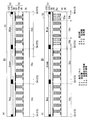
右眼用サブ画素領域23R及び左眼用サブ画素領域23Lの横幅は、互いに同一またはほぼ同一に設定される。このように構成されたサブ画素領域23R及び23Lは表示パネル20において横方向に所定の均一なピッチで配列されている。なお、実施の形態1では、サブ画素領域23R及び23Lは、横方向だけでなく縦方向にも配列されている。 The horizontal widths of the right-eye sub-pixel region 23R and the left-eye sub-pixel region 23L are set to be the same or substantially the same. The constructed sub pixel regions 23R and 23L as are arranged at a predetermined uniform pitch in the horizontal direction in the display panel 20. In the first embodiment, sub-pixel regions 23R and 23L are arranged in the vertical direction as well as laterally.
実施の形態1では、視差バリアパネル30の液晶モードとしてTN(Twisted Nematic)モードを採用した。上述したストライプ状透明電極と、対向透明電極間に電圧を選択的に印加すると、電圧印加領域のみ遮光状態となり、2画像表示(3次元画像(第2形式の画像)を表示)するのに必要な視差バリア・ストライプ(遮蔽領域33Sと透過領域33Tとが混在する一部遮光状態)を形成できる。全てのストライプ状透明電極,対向透明電極に電圧を印加しない状態とすることで、視差バリアパネル30全面を透過状態(完全光透過状態)とすることができ、単一画像(2次元画像;第1形式の画像)を表示できる。 In the first embodiment, a TN (Twisted Nematic) mode is adopted as the liquid crystal mode of the parallax barrier panel 30. When a voltage is selectively applied between the above-described stripe-shaped transparent electrode and the counter transparent electrode, only the voltage application region is in a light-shielded state, which is necessary for displaying two images (displaying a three-dimensional image (second format image)). parallax barrier stripes that can form a (shielded region 33S and the transmissive region 33 T is partially blocked state mixed). By setting a state in which no voltage is applied to all the striped transparent electrodes and the counter transparent electrodes, the entire surface of the parallax barrier panel 30 can be set to a transmission state (complete light transmission state), and a single image (two-dimensional image; 1 format image) can be displayed.
すなわち、表示パネル20の2画像表示時は、複数の画素それぞれの画素周辺領域を強制的に黒表示状態に設定することにより水平方向(横方向)の遮光性を高めた画像表示を行い、表示パネル20の単一画像表示時は、複数の画素それぞれの画素周辺領域の輝度を画素主要領域と同じ輝度に設定することにより輝度を高めた画像表示を行うことができる。 That is, when two images are displayed on the display panel 20, image display with improved light shielding in the horizontal direction (lateral direction) is performed by forcibly setting the pixel peripheral area of each of the plurality of pixels to a black display state. When displaying a single image on the panel 20, it is possible to display an image with increased brightness by setting the brightness of the pixel peripheral area of each of the plurality of pixels to the same brightness as the main pixel area.
本実施の形態の特徴的な構造として、色成分であるR,G,B(Red、Green、Blue)用のカラーフィルタ層57の色材膜57Cを用いて色表示する液晶パネル各画素の透明基板52側に対向透明電極44を液晶層53の画素周辺領域に対応する領域に配置している。すなわち、実施の形態1と同様、通常のIn-Plane Switchingモード液晶パネルでは設けない対向透明電極44を形成している。なお、図5で示す構成では、対向透明電極44はカラーフィルタ層57(遮光膜57S,色材膜57C(RGB用))及びオーバーコート58を介して透明基板52上に形成される。また、透明基板52に対向する下側の透明基板55上に実施の形態1と同様に櫛歯電極45が設けられ、櫛歯電極45を含む透明基板55上に液晶層53が設けられる。
As a characteristic structure of the present embodiment, each pixel of a liquid crystal panel that performs color display using a
図6は画素周辺領域制御部62が色成分別輝度設定処理を実行する際の複数の対向透明電極44に対する電圧制御内容を模式的に示す説明図である。以下、説明の都合上、R用(色材膜57Cが赤色(Red))の対向透明電極44を対向透明電極44R、G用(色材膜57Cが緑(Green))の対向透明電極44を対向透明電極44G、B用(色材膜57Cが青(Blue))の対向透明電極44を対向透明電極44Bとして示している。マトリクス状に配列される複数の画素それぞれに、図5に示すように、R用、G用及びB用の対向透明電極44R、対向透明電極44G及び対向透明電極44Bが設けられる。
FIG. 6 is an explanatory diagram schematically illustrating voltage control contents for the plurality of counter
したがって、複数の対向透明電極44Rはそれぞれ対応するR用の画素の画素周辺領域の液晶分子53eを制御可能に独立して設けられ、複数の対向透明電極44Gは対応するG用の画素の画素周辺領域の液晶分子53eを制御可能に独立して設けられ、複数の対向透明電極44Bは対応するB用の画素の画素周辺領域の液晶分子53eを制御可能に独立して設けられる。 Therefore, a plurality of opposed transparent electrodes 44R are provided respectively corresponding liquid crystal molecules 5 3e pixel peripheral region of the pixel for R controllably independently, the plurality of opposed transparent electrodes 44G pixels of the pixel for the corresponding G controllably independently provided liquid crystal molecules 5 3e the peripheral region, a plurality of opposed transparent electrode 44B is provided to controllably independent liquid crystal molecules 5 3e pixel peripheral region of pixels for the corresponding B.
一方、画素周辺領域制御部62はRGBのいずれかの輝度を製造時より低下させて色表示の調整を行う必要がある場合、対向透明電極群144R,144G及び144Bのうち輝度低下対象の対向透明電極群144の複数の対向透明電極44(44R,44G,44Bのうち少なくとも一つ)に対して、黒表示用電圧VAの制御電圧V62(V62R,V62G及びV62Bの少なくとも一つ)を付与する。ここで、B用の輝度を低下させる場合を考える。
On the other hand, if the pixel peripheral region control unit 62 which is necessary to lower Ri by the time of manufacture of any of the luminance of RGB to adjust the color display, counter transparent electrodes 144R, 144G and opposing luminance reduction target of 144B a plurality of counter
画素周辺領域制御部62は、RGBのうちBの色調整の必要がある場合、対向透明電極群144Bの対向透明電極44Bに対し共通に設定された黒表示用電圧VAの制御電圧V62Bを付与する。黒表示用電圧VAは、実施の形態1と同様、櫛歯電極45の白表示時の電圧設定状態(正極性,負極性の電圧設定状態)を考慮して、対向透明電極44下の液晶分子23eが立ち上がる遮光状態に設定可能な電界が対向透明電極44B,櫛歯電極45間に生じるように可変設定される。なお、正極性,負極性となるタイミング制御は、表示のために櫛歯電極45に印加する電圧の駆動信号の極性切替えと同期させて、対向透明電極群144Bへ黒表示用電圧VAを供給する駆動信号である制御電圧V62Bを切替え変動させれば良い。
The pixel peripheral area control unit 62 applies the control voltage V62B of the black display voltage VA that is set in common to the counter transparent electrode 44B of the counter transparent electrode group 144B when it is necessary to adjust the color B of RGB. . As in the first embodiment, the black display voltage VA is a liquid crystal molecule below the counter
この際、前述したように、画素電極,共通電極間の白表示時における横電界の極性を考慮して対向透明電極44B,櫛歯電極45間に常に高い電界を発生させることができる黒表示用電圧VAを設定する。その結果、透明基板52に設けた対向透明電極44Bに対応する画素周辺領域は、画素周辺領域以外の画素主要領域の表示状態に依存せず、常に黒表示にすることにより、実質的にB用の画素の開口率を小さくし、B用画素の輝度を装置完成時より低く設定することによりRGB色表示に関する色調整を行うことができる。
At this time, as described above, in consideration of the polarity of the horizontal electric field during white display between the pixel electrode and the common electrode, the black display capable of always generating a high electric field between the counter transparent electrode 44 B and the
Claims (5)
前記複数の画素それぞれの周辺部である画素周辺領域の輝度を、前記画素周辺領域以外の画素主要領域と独立して制御する画素周辺領域輝度制御手段とを備える、
表示装置。 A display panel for displaying an image with a plurality of pixels arranged in a matrix;
Pixel peripheral region luminance control means for controlling the luminance of the pixel peripheral region, which is the peripheral part of each of the plurality of pixels, independently of the pixel main region other than the pixel peripheral region;
Display device.
前記表示パネルの前方または後方に配置され、第1形式の画像用に設定される完全光透過状態と、第2形式の画像用に設定される、水平方向に沿って透過領域と遮光領域とが交互に形成される一部遮光状態とを切り替え可能な視差バリアパネルをさらに備え、
前記表示パネルにおける前記複数の画素は、前記第2形式の画像表示用に役割が分担された第1種画素と第2種画素とが前記水平方向に交互に配列されており、
前記画素周辺領域は前記複数の画素それぞれの前記水平方向における両端部領域を少なくとも含み、
前記画素周辺領域輝度制御手段は、
前記複数の画素に対し、前記視差バリアパネルの前記一部遮光状態時に前記画素周辺領域を強制的に黒表示状態に設定し、前記視差バリアパネルの前記完全光透過状態時に前記画素周辺領域の輝度を前記画素主要領域と同じ輝度に設定する輝度設定処理を実行する、
表示装置。 The display device according to claim 1,
A completely light transmissive state that is disposed in front of or behind the display panel and is set for a first type image, and a transmissive region and a light shielding region that are set for a second type image along a horizontal direction. It further includes a parallax barrier panel capable of switching between partially formed light blocking states,
The plurality of pixels in the display panel are alternately arranged in the horizontal direction with first type pixels and second type pixels each having a role shared for image display of the second format,
The pixel peripheral region includes at least both end regions in the horizontal direction of the plurality of pixels,
The pixel peripheral area luminance control means includes:
Wherein the plurality of pixels, the parallax setting the pixel peripheral region the during partial blocking state of the barrier panel to forcibly black display state, the luminance of the pixel peripheral region during the complete light transmission state of the parallax barrier panel A brightness setting process for setting the same brightness as that of the pixel main region,
Display device.
前記表示パネルは、
一方電極,他方電極間に形成される電界によって状態が変化する液晶層により前記複数の画素が構成される液晶表示パネルであり、
前記画素周辺領域輝度制御手段は、
前記複数の画素それぞれの前記画素周辺領域に対応して独立して設けられる複数の画素周辺領域用電極を含み、前記画素周辺領域用電極は、前記一方電極及び他方電極のいずれかの電極との間で前記液晶層に電界を発生させることができ、
前記複数の周辺領域用電極に付与する電圧状態を前記視差バリアパネルの前記一部遮光状態時と前記完全光透過状態時とで変化させることにより、前記輝度設定処理を実行する画素周辺領域用電極制御部をさらに含む、
表示装置。 The display device according to claim 2, wherein
The display panel is
A liquid crystal display panel in which the plurality of pixels are configured by a liquid crystal layer whose state is changed by an electric field formed between one electrode and the other electrode;
The pixel peripheral area luminance control means includes:
Includes a plurality of pixels peripheral area electrodes provided independently in correspondence with the pixel peripheral region of said plurality of pixels respectively, said pixel peripheral region for electrodes, with one electrode of the one electrode and the other electrode An electric field can be generated between the liquid crystal layers,
A pixel peripheral region electrode that executes the luminance setting process by changing a voltage state applied to the plurality of peripheral region electrodes between the partial light blocking state and the complete light transmitting state of the parallax barrier panel. further comprising a control unit,
Display device.
前記複数の画素はそれぞれ複数種の色成分画素を有し、
前記画素周辺領域輝度制御手段は、
前記複数の画素に対し、前記複数種の色成分画素単位に、前記画素周辺領域の輝度を強制的に黒表示状態にする第1設定、及び前記画素周辺領域の輝度を前記画素主要領域と同じにする第2設定のいずれかに設定する、色成分別輝度設定処理を実行する、
表示装置。 The display device according to claim 1,
Each of the plurality of pixels has a plurality of types of color component pixels,
The pixel peripheral area luminance control means includes:
For the plurality of pixels, a first setting for forcibly setting the luminance of the pixel peripheral region to a black display state in units of the plurality of types of color component pixels, and the luminance of the pixel peripheral region the same as the main pixel region Set to any one of the second settings to be performed, execute the luminance setting processing for each color component,
Display device.
前記表示パネルは、
一方電極,他方電極間に形成される電界によって状態が変化する液晶層により前記複数の画素が構成される液晶表示パネルであり、
前記画素周辺領域輝度制御手段は、
前記複数の画素それぞれの前記画素周辺領域に対応して独立して設けられる複数の画素周辺領域用電極を含み、前記複数の画素周辺領域用電極はそれぞれ前記複数種の色成分に対応する複数種の色成分画素用電極を有し、前記複数種の色成分画素用電極はそれぞれ前記一方電極及び他方電極のいずれかの電極との間で前記液晶層に電界を発生させることができ、
前記複数の画素周辺領域用電極に付与する電圧状態を前記複数種の色成分画素用電極単位に設定することにより、前記色成分別輝度設定処理を実行する画素周辺領域制御部をさらに含む、
表示装置。 The display device according to claim 4,
The display panel is
A liquid crystal display panel in which the plurality of pixels are configured by a liquid crystal layer whose state is changed by an electric field formed between one electrode and the other electrode;
The pixel peripheral area luminance control means includes:
A plurality of pixel peripheral region electrodes provided independently corresponding to the pixel peripheral region of each of the plurality of pixels, wherein the plurality of pixel peripheral region electrodes are respectively a plurality of types corresponding to the plurality of types of color components Each of the plurality of color component pixel electrodes can generate an electric field in the liquid crystal layer between each of the one electrode and the other electrode,
A pixel peripheral region control unit that executes the luminance setting processing for each color component by setting a voltage state to be applied to the plurality of pixel peripheral region electrodes in units of the plurality of types of color component pixel electrodes;
Display device.
Priority Applications (3)
| Application Number | Priority Date | Filing Date | Title |
|---|---|---|---|
| JP2012284588A JP6124587B2 (en) | 2012-12-27 | 2012-12-27 | Display device |
| US14/103,720 US9349337B2 (en) | 2012-12-27 | 2013-12-11 | Display device |
| US15/077,556 US9412312B2 (en) | 2012-12-27 | 2016-03-22 | Display device |
Applications Claiming Priority (1)
| Application Number | Priority Date | Filing Date | Title |
|---|---|---|---|
| JP2012284588A JP6124587B2 (en) | 2012-12-27 | 2012-12-27 | Display device |
Publications (3)
| Publication Number | Publication Date |
|---|---|
| JP2014126764A JP2014126764A (en) | 2014-07-07 |
| JP2014126764A5 true JP2014126764A5 (en) | 2016-01-28 |
| JP6124587B2 JP6124587B2 (en) | 2017-05-10 |
Family
ID=51016708
Family Applications (1)
| Application Number | Title | Priority Date | Filing Date |
|---|---|---|---|
| JP2012284588A Active JP6124587B2 (en) | 2012-12-27 | 2012-12-27 | Display device |
Country Status (2)
| Country | Link |
|---|---|
| US (2) | US9349337B2 (en) |
| JP (1) | JP6124587B2 (en) |
Families Citing this family (11)
| Publication number | Priority date | Publication date | Assignee | Title |
|---|---|---|---|---|
| JP6099892B2 (en) * | 2012-07-09 | 2017-03-22 | パナソニック インテレクチュアル プロパティ コーポレーション オブ アメリカPanasonic Intellectual Property Corporation of America | Video display device |
| JP6207355B2 (en) * | 2013-11-18 | 2017-10-04 | 株式会社ジャパンディスプレイ | 3D display device |
| CN104267525B (en) * | 2014-08-18 | 2018-05-11 | 深圳市华星光电技术有限公司 | 3 d display device and preparation method thereof |
| CN104460013B (en) * | 2014-12-10 | 2016-11-30 | 深圳市华星光电技术有限公司 | 3D display device based on lens switching integration imaging and display packing |
| CN104597610B (en) * | 2015-02-10 | 2016-12-07 | 京东方科技集团股份有限公司 | The display processing method of a kind of bore hole 3D, device and display device |
| CN104808350B (en) * | 2015-05-13 | 2018-01-09 | 京东方科技集团股份有限公司 | Display base plate and preparation method thereof, display drive method, display device |
| WO2018090552A1 (en) * | 2016-11-21 | 2018-05-24 | 华为技术有限公司 | Method for controlling screen of intelligent device, and intelligent device |
| TWI633791B (en) * | 2017-10-16 | 2018-08-21 | 國立成功大學 | Rgb format adjustment and reconstruction method and circuit for depth frame packing and depacking |
| CN110504126B (en) * | 2018-05-16 | 2021-07-27 | 无锡小天鹅电器有限公司 | Control panel, household appliance and control method of household appliance |
| CN109256076B (en) * | 2018-08-30 | 2022-02-22 | 京东方科技集团股份有限公司 | Edge pixel display method, system, storage device and display device |
| CN112526763B (en) * | 2020-11-20 | 2022-09-27 | 亿信科技发展有限公司 | Light field 3D display device and driving method thereof |
Family Cites Families (10)
| Publication number | Priority date | Publication date | Assignee | Title |
|---|---|---|---|---|
| JP2857429B2 (en) | 1989-10-02 | 1999-02-17 | 日本放送協会 | Three-dimensional image display apparatus and method |
| JPH04145416A (en) | 1990-10-05 | 1992-05-19 | Fujitsu Ltd | Color display element |
| JP2005164916A (en) * | 2003-12-02 | 2005-06-23 | Canon Inc | Stereoscopic display device |
| JP2007017822A (en) * | 2005-07-11 | 2007-01-25 | Sanyo Epson Imaging Devices Corp | Display apparatus |
| JP2009204899A (en) * | 2008-02-28 | 2009-09-10 | Epson Imaging Devices Corp | Electrooptical device, elecronic equipment and driving method of electrooptical device |
| KR101354329B1 (en) * | 2009-04-17 | 2014-01-22 | 엘지디스플레이 주식회사 | Image display device |
| WO2011010637A1 (en) * | 2009-07-22 | 2011-01-27 | シャープ株式会社 | Method for manufacturing liquid crystal display device |
| JP6147953B2 (en) * | 2011-03-15 | 2017-06-14 | 株式会社ジャパンディスプレイ | Display device |
| JP6042102B2 (en) * | 2012-05-24 | 2016-12-14 | パナソニック インテレクチュアル プロパティ コーポレーション オブ アメリカPanasonic Intellectual Property Corporation of America | Video display device |
| JP6057647B2 (en) * | 2012-09-27 | 2017-01-11 | 三菱電機株式会社 | Display device |
-
2012
- 2012-12-27 JP JP2012284588A patent/JP6124587B2/en active Active
-
2013
- 2013-12-11 US US14/103,720 patent/US9349337B2/en active Active
-
2016
- 2016-03-22 US US15/077,556 patent/US9412312B2/en active Active
Similar Documents
| Publication | Publication Date | Title |
|---|---|---|
| JP2014126764A5 (en) | ||
| JP6124587B2 (en) | Display device | |
| JP5667752B2 (en) | 3D image display device | |
| TWI480588B (en) | Display device | |
| JP6018057B2 (en) | Video display device and video display method | |
| JP6258233B2 (en) | 3D display method and display device | |
| JP5701389B2 (en) | 3D display device | |
| US20130050284A1 (en) | Display device and electronic unit | |
| JP5779533B2 (en) | Display device | |
| JP4483181B2 (en) | 3D image display device | |
| JP6223158B2 (en) | Liquid crystal display | |
| JP2011169949A (en) | Three-dimensional image display device | |
| JP2013231745A (en) | Stereoscopic display device | |
| US20150077665A1 (en) | 3d display apparatus and method for manufacturing the same | |
| WO2013031592A1 (en) | 3d display device | |
| JP5789553B2 (en) | Display device | |
| WO2015083522A1 (en) | Image display apparatus | |
| JP4111206B2 (en) | Image display device | |
| US9606367B2 (en) | Stereoscopic display device | |
| KR102153605B1 (en) | Three dimensional image display device | |
| WO2017122595A1 (en) | Display device and liquid crystal panel driving method | |
| WO2013143196A1 (en) | 3d liquid crystal panel, 3d liquid crystal display device and driving method | |
| JP4894314B2 (en) | Image display device | |
| KR101469474B1 (en) | Display device | |
| US20130265510A1 (en) | Three-dimensional display device and active optical element thereof |