JP2014116502A - Multilayer capacitor - Google Patents

Multilayer capacitor Download PDF

Info

Publication number
JP2014116502A
JP2014116502A JP2012270443A JP2012270443A JP2014116502A JP 2014116502 A JP2014116502 A JP 2014116502A JP 2012270443 A JP2012270443 A JP 2012270443A JP 2012270443 A JP2012270443 A JP 2012270443A JP 2014116502 A JP2014116502 A JP 2014116502A
Authority
JP
Japan
Prior art keywords
electrode
electrode layer
main
element body
multilayer capacitor
Prior art date
Legal status (The legal status is an assumption and is not a legal conclusion. Google has not performed a legal analysis and makes no representation as to the accuracy of the status listed.)
Granted
Application number
JP2012270443A
Other languages
Japanese (ja)
Other versions
JP6263834B2 (en
Inventor
Takeshi Onuma
岳史 大沼
Current Assignee (The listed assignees may be inaccurate. Google has not performed a legal analysis and makes no representation or warranty as to the accuracy of the list.)
TDK Corp
Original Assignee
TDK Corp
Priority date (The priority date is an assumption and is not a legal conclusion. Google has not performed a legal analysis and makes no representation as to the accuracy of the date listed.)
Filing date
Publication date
Application filed by TDK Corp filed Critical TDK Corp
Priority to JP2012270443A priority Critical patent/JP6263834B2/en
Publication of JP2014116502A publication Critical patent/JP2014116502A/en
Application granted granted Critical
Publication of JP6263834B2 publication Critical patent/JP6263834B2/en
Active legal-status Critical Current
Anticipated expiration legal-status Critical

Links

Images

Abstract

PROBLEM TO BE SOLVED: To provide a multilayer capacitor in which intrusion of an acidic liquid can be reduced, while maintaining adhesion of a terminal electrode and an element.SOLUTION: A multilayer capacitor 1 comprises: an element 2; first and second terminal electrodes 5, 6; and first and second internal electrodes 3, 4. The first and second internal electrodes 3, 4 have main electrodes 3a, 4a facing each other, and lead-out portions 3b, 4b led out from the main electrodes 3a, 4a to the end faces 2a, 2b or the side faces 2e, 2f of the element 2, and connected with corresponding internal electrodes, respectively. The first and second terminal electrodes 5, 6 have first baked electrode layers 5a, 6a, and second baked electrode layers 5b, 6b, respectively. The first baked electrode layers 5a, 6a have a content ratio of glass component lower than that of the second baked electrode layers 5b, 6b.

Description

本発明は、積層コンデンサに関する。   The present invention relates to a multilayer capacitor.

従来の積層コンデンサとしては、例えば特許文献1に記載されたものが知られている。特許文献1に記載の積層コンデンサは、素体と、素体内に配置された内部電極と、素体の両端部に配置され且つ内部電極が接続される端子電極と、を備えている。この積層コンデンサでは、端子電極は、導電性ペーストを焼き付けて形成されている。   As a conventional multilayer capacitor, for example, the one described in Patent Document 1 is known. The multilayer capacitor described in Patent Document 1 includes an element body, internal electrodes disposed in the element body, and terminal electrodes disposed at both ends of the element body and connected to the internal electrodes. In this multilayer capacitor, the terminal electrode is formed by baking a conductive paste.

特開2010−129737号公報JP 2010-129737 A

上記の積層コンデンサのように、導電性ペーストを焼き付けて端子電極を形成する構成では、端子電極と素体との密着性を確保するために、端子電極にガラス成分を多く含ませることがある。この場合、積層コンデンサでは、素体と端子電極との密着性は向上するが、内部電極と端子電極との接続性が低下するおそれがある。   In the configuration in which the terminal electrode is formed by baking the conductive paste as in the above-described multilayer capacitor, the terminal electrode may contain a large amount of glass component in order to ensure the adhesion between the terminal electrode and the element body. In this case, in the multilayer capacitor, the adhesion between the element body and the terminal electrode is improved, but the connectivity between the internal electrode and the terminal electrode may be reduced.

本発明は、上記課題を解決するためになされたものであり、端子電極と内部電極との接続性を維持しつつ、端子電極の密着性の向上を図れる積層コンデンサを提供することを目的とする。   The present invention has been made to solve the above-described problems, and an object of the present invention is to provide a multilayer capacitor capable of improving the adhesion of the terminal electrode while maintaining the connectivity between the terminal electrode and the internal electrode. .

本発明に係る積層コンデンサは、互いに対向する一対の端面と、一対の端面間を連結するように伸び且つ互いに対向する一対の主面と、一対の主面間を連結するように伸び且つ互いに対向する一対の側面とを有し、一対の主面の間の寸法が一対の端面の間の寸法、及び一対の側面の間の寸法よりも小さい素体と、素体の両端部に位置し、主面と端面及び側面の少なくとも一方とにわたって連続して配置される第1及び第2の端子電極と、第1及び第2の端子電極のうち対応する端子電極に接続され、一対の主面が対向する方向で互いに対向するように素体内に配置される第1及び第2の内部電極と、を備え、第1及び第2の内部電極は、互いに対向する主電極部と、主電極部から素体の端面又は側面に引き出されて対応する端子電極に接続される引き出し部と、をそれぞれ有し、第1及び第2の端子電極は、少なくとも引き出し部を覆って配置され且つ導電性ペーストを焼付けて形成された第1焼付電極層と、少なくとも第1焼付電極層上に配置され且つガラス成分を含む導電性ペーストを焼付けて形成された第2焼付電極層と、をそれぞれ有することを特徴とする。   The multilayer capacitor according to the present invention extends so as to connect a pair of end faces, a pair of main faces facing each other, and a pair of main faces, and extends so as to connect between the pair of main faces. A pair of side surfaces, the dimension between the pair of main surfaces is smaller than the dimension between the pair of end surfaces, and the dimension between the pair of side surfaces, and located at both ends of the element body, The first and second terminal electrodes arranged continuously over at least one of the main surface, the end surface, and the side surface, and the corresponding terminal electrode among the first and second terminal electrodes are connected, and the pair of main surfaces are First and second internal electrodes disposed in the element body so as to face each other in opposite directions, and the first and second internal electrodes include a main electrode portion facing each other, and a main electrode portion It is pulled out to the end face or side face of the element body and connected to the corresponding terminal electrode. Each of the first and second terminal electrodes is disposed so as to cover at least the lead portion and is formed by baking a conductive paste, and at least the first baking electrode. And a second baked electrode layer formed by baking a conductive paste disposed on the layer and containing a glass component.

この積層コンデンサでは、第1焼付電極層は、ガラス成分を含まない、あるいはガラス成分の含有量が少なくてもよい。これにより、積層コンデンサでは、第1焼付電極層の金属の含有率を比較的高くできるため、第1及び第2の端子電極と第1及び第2の内部電極との接続性を維持できる。また、積層コンデンサでは、第2焼付電極層がガラス成分を含んでいるため、素体や第1焼付電極層との密着性が確保される。したがって、第1及び第2の端子電極の密着性の向上が図れる。   In this multilayer capacitor, the first baking electrode layer may not contain a glass component or may contain a small amount of glass component. Thereby, in the multilayer capacitor, the metal content of the first baking electrode layer can be made relatively high, so that the connectivity between the first and second terminal electrodes and the first and second internal electrodes can be maintained. In the multilayer capacitor, since the second baking electrode layer contains a glass component, adhesion with the element body and the first baking electrode layer is ensured. Therefore, the adhesion between the first and second terminal electrodes can be improved.

第1焼付電極層は、ガラス成分を含む導電性ペーストを焼付けて形成されており、第1焼付電極層のガラス成分の含有比率は、第2焼付電極層のガラス成分の含有比率よりも低いことが好ましい。このように、積層コンデンサでは、第1焼付電極層がガラス成分を多少含むことにより、第1焼付電極層と第2焼付電極層との密着性の向上がより一層図れる。   The first baking electrode layer is formed by baking a conductive paste containing a glass component, and the content ratio of the glass component of the first baking electrode layer is lower than the content ratio of the glass component of the second baking electrode layer. Is preferred. As described above, in the multilayer capacitor, the first baked electrode layer contains some glass components, whereby the adhesion between the first baked electrode layer and the second baked electrode layer can be further improved.

また、積層コンデンサでは、素体は、一対の主面の間の寸法が一対の端面の間の寸法、及び一対の側面の間の寸法よりも小さい。このように、いわゆる低背型の積層コンデンサとして構成し、第1及び第2の端子電極を少なくとも主面に配置することにより、回路基板への内蔵やLSI(Large Scale Integration)への埋め込み実装が可能となる。また、積層コンデンサを埋め込む構造では、主面の端子電極とビア導体が接続される。このような実装構造では、端子電極の電流ループ距離が短くなるため、等価直列インダクタンス(ESL)を低くできる。   In the multilayer capacitor, the dimension of the element body is smaller than the dimension between the pair of end surfaces and the dimension between the pair of side surfaces. In this way, it is configured as a so-called low-profile multilayer capacitor, and the first and second terminal electrodes are arranged on at least the main surface, so that they can be embedded in a circuit board or embedded in an LSI (Large Scale Integration). It becomes possible. In the structure in which the multilayer capacitor is embedded, the terminal electrode on the main surface and the via conductor are connected. In such a mounting structure, since the current loop distance of the terminal electrode is shortened, the equivalent series inductance (ESL) can be lowered.

第1焼付電極層は、素体の主面と引き出し部が引き出された素体の端面又は側面とにわたって連続して配置され、第2焼付電極層は、第1焼付電極層が配置された素体の端面側又は側面側に配置されていてもよい。このような構成により、積層コンデンサでは、主面に第1焼付電極層が配置されるため、第1及び第2の端子電極の主面側の平滑性を確保できる。また、積層コンデンサでは、素体の主面に第2焼付電極層がほとんど配置されないため、第1及び第2の端子電極の主面側の厚みを小さくできる。   The first baked electrode layer is continuously arranged over the main surface of the element body and the end surface or side surface of the element body from which the lead portion is drawn, and the second baked electrode layer is an element on which the first baked electrode layer is arranged. You may arrange | position at the end surface side or side surface side of a body. With such a configuration, in the multilayer capacitor, since the first baking electrode layer is disposed on the main surface, the smoothness on the main surface side of the first and second terminal electrodes can be ensured. In the multilayer capacitor, since the second baking electrode layer is hardly disposed on the main surface of the element body, the thickness on the main surface side of the first and second terminal electrodes can be reduced.

第1焼付電極層は、引き出し部が引き出された素体の端面又は側面に配置され、第2焼付電極層は、素体の主面と第1焼付電極層が配置された素体の端面側又は側面側とにわたって連続して配置されていてもよい。このような構成により、積層コンデンサでは、素体の主面に第1焼付電極層がほとんど配置されないため、第1及び第2の端子電極の主面側の厚みを小さくできる。また、積層コンデンサでは、ガラス成分の含有比率が比較的高い第2焼付電極層が素体の主面に配置されるため、第1及び第2の端子電極の主面側(ビア導体とのコンタクト部分)において第1及び第2の端子電極と素体との密着性を確保できる。   The first baked electrode layer is disposed on the end surface or the side surface of the element body from which the lead portion is drawn, and the second baked electrode layer is the end surface side of the element body on which the main surface of the element body and the first baked electrode layer are disposed. Or you may arrange | position continuously over the side surface side. With such a configuration, in the multilayer capacitor, since the first baking electrode layer is hardly disposed on the main surface of the element body, the thickness of the main surface side of the first and second terminal electrodes can be reduced. In the multilayer capacitor, since the second baking electrode layer having a relatively high glass component content ratio is disposed on the main surface of the element body, the main surface side of the first and second terminal electrodes (contact with the via conductor) In the portion), the adhesion between the first and second terminal electrodes and the element body can be secured.

引き出し部は、側面に引き出されていることが好ましい。このような構成により、積層コンデンサでは、第1及び第2の端子電極の引き出し部の間の距離を小さくすることができるので、低ESLとすることができる。   It is preferable that the drawer part is pulled out to the side surface. With such a configuration, in the multilayer capacitor, the distance between the lead portions of the first and second terminal electrodes can be reduced, so that the ESL can be reduced.

主面に配置される第1及び第2端子電極の一対の側面の対向方向での幅は、第1端子電極と第2端子電極との離間距離よりも大きいことが好ましい。このような構成により、積層コンデンサでは、端子電極の主面側の面積が大きくなるため、回路基板に内蔵実装する際に、ビア導体との接続をより確実に行うことができる。   The width of the pair of side surfaces of the first and second terminal electrodes arranged on the main surface in the facing direction is preferably larger than the distance between the first terminal electrode and the second terminal electrode. With such a configuration, in the multilayer capacitor, the area on the main surface side of the terminal electrode is increased, and therefore, the connection with the via conductor can be more reliably performed when the multilayer capacitor is mounted in the circuit board.

主面に配置される第1及び第2端子電極の一対の端面の対向方向での幅は、第1端子電極と第2端子電極との離間距離よりも大きいことが好ましい。このような構成により、積層コンデンサでは、端子電極の主面側の面積が大きくなるため、回路基板に内蔵実装する際に、ビア導体との接続をより確実に行うことができる。   The width in the opposing direction of the pair of end faces of the first and second terminal electrodes arranged on the main surface is preferably larger than the separation distance between the first terminal electrode and the second terminal electrode. With such a configuration, in the multilayer capacitor, the area on the main surface side of the terminal electrode is increased, and therefore, the connection with the via conductor can be more reliably performed when the multilayer capacitor is mounted in the circuit board.

第1及び第2の内部電極のうち一方の主面に最も近い内部電極と一方の主面との間の寸法、及び、第1及び第2の内部電極のうち他方の主面に最も近い内部電極と他方の主面との間の寸法は、一方の主面に最も近い内部電極と他方の主面に最も近い内部電極との間の寸法と略同等であることが好ましい。このような構成により、積層コンデンサでは、外層厚みと内層厚みの両方を厚くできるので、応力緩和しつつ静電容量を大きくできる。   Of the first and second internal electrodes, the dimension between the internal electrode closest to one main surface and one main surface, and the internal closest to the other main surface of the first and second internal electrodes The dimension between the electrode and the other main surface is preferably substantially the same as the dimension between the inner electrode closest to one main surface and the inner electrode closest to the other main surface. With such a configuration, in the multilayer capacitor, both the outer layer thickness and the inner layer thickness can be increased, so that the capacitance can be increased while relaxing the stress.

第1及び第2焼付電極層上にめっき層が配置されていることが好ましい。このような構成により、積層コンデンサでは、回路基板に実装する際、ビア導体とめっき層とが接続されるため、ビア導体と端子電極との接続強度を確保できる。   It is preferable that the plating layer is arrange | positioned on the 1st and 2nd baking electrode layer. With such a configuration, when the multilayer capacitor is mounted on a circuit board, the via conductor and the plating layer are connected, so that the connection strength between the via conductor and the terminal electrode can be ensured.

第1及び第2焼付電極層の少なくとも一方と回路基板のビア導体とが直接接続される構成とすることができる。このような構成によれば、めっき層の形成が不要となる。   At least one of the first and second baked electrode layers and the via conductor of the circuit board can be directly connected. According to such a configuration, it is not necessary to form a plating layer.

本発明に係る積層コンデンサは、互いに対向する一対の端面と、一対の端面間を連結するように伸び且つ互いに対向する一対の主面と、一対の主面間を連結するように伸び且つ互いに対向する一対の側面とを有し、一対の主面の間の寸法が一対の端面の間の寸法、及び前記一対の側面の間の寸法よりも小さい素体と、素体の両端部に位置し、主面と端面及び側面の少なくとも一方とにわたって連続して配置される第1及び第2の端子電極と、第1及び第2の端子電極のうち対応する端子電極に接続され、一対の主面が対向する方向で互いに対向するように素体内に配置される第1及び第2の内部電極と、を備え、第1及び第2の内部電極は、互いに対向する主電極部と、主電極部から素体の端面又は側面に引き出され対応する端子電極に接続される引き出し部と、をそれぞれ有し、第1及び第2の端子電極は、引き出し部との接合領域に配置される第1の領域と、ガラス成分を含み且つ第1及び第2の端子電極の外表面側に配置される第2の領域と、をそれぞれ有することを特徴とする。   The multilayer capacitor according to the present invention extends so as to connect a pair of end faces, a pair of main faces facing each other, and a pair of main faces, and extends so as to connect between the pair of main faces. An element body having a dimension between the pair of main faces smaller than a dimension between the pair of end faces and a dimension between the pair of side faces, and positioned at both ends of the element body. The first and second terminal electrodes arranged continuously across at least one of the main surface, the end surface and the side surface, and a pair of main surfaces connected to the corresponding terminal electrode among the first and second terminal electrodes First and second internal electrodes disposed in the element body so as to face each other in a direction opposite to each other, the first and second internal electrodes comprising a main electrode part facing each other, and a main electrode part Is pulled out from the end face or side of the element body and connected to the corresponding terminal electrode Each of the first and second terminal electrodes includes a first region disposed in a bonding region with the lead portion, a glass component, and the first and second terminal electrodes. And a second region disposed on the outer surface side.

この積層コンデンサでは、引き出し部との接合領域に配置される第1領域は、ガラス成分を含まない、あるいはガラス成分の含有量が少なくてもよい。これにより、積層コンデンサでは、第1領域の金属の含有率を比較的高くできるため、第1及び第2の端子電極と第1及び第2の内部電極との接続性を維持できる。また、積層コンデンサでは、第2領域がガラス成分を含んでいるため、素体や第1領域との密着性が確保される。したがって、第1及び第2の端子電極の密着性の向上が図れる。   In this multilayer capacitor, the first region arranged in the junction region with the lead portion does not contain a glass component or may contain a small amount of glass component. Thereby, in the multilayer capacitor, the metal content in the first region can be made relatively high, so that the connectivity between the first and second terminal electrodes and the first and second internal electrodes can be maintained. Further, in the multilayer capacitor, the second region contains a glass component, so that the adhesion with the element body and the first region is ensured. Therefore, the adhesion between the first and second terminal electrodes can be improved.

本発明によれば、端子電極と内部電極との接続性を維持しつつ、端子電極の密着性の向上を図れる。   ADVANTAGE OF THE INVENTION According to this invention, the adhesiveness of a terminal electrode can be improved, maintaining the connectivity of a terminal electrode and an internal electrode.

第1実施形態に係る積層コンデンサを示す斜視図である。1 is a perspective view showing a multilayer capacitor according to a first embodiment. 図1に示す積層コンデンサのII−II線での断面構成を示す図である。It is a figure which shows the cross-sectional structure in the II-II line of the multilayer capacitor shown in FIG. 図1に示す積層コンデンサのIII−III線での断面構成を示す図である。It is a figure which shows the cross-sectional structure in the III-III line of the multilayer capacitor shown in FIG. 図1に示す積層コンデンサの素体の分解斜視図である。FIG. 2 is an exploded perspective view of an element body of the multilayer capacitor shown in FIG. 1. 図1に示す積層コンデンサの実装構造の断面構成を示す図である。It is a figure which shows the cross-sectional structure of the mounting structure of the multilayer capacitor shown in FIG. 積層コンデンサの変形例の断面構成を示す図である。It is a figure which shows the cross-sectional structure of the modification of a multilayer capacitor. 図6に示す積層コンデンサの実装構造の断面構成を示す図である。It is a figure which shows the cross-sectional structure of the mounting structure of the multilayer capacitor shown in FIG. 第2実施形態に係る積層コンデンサの断面構成を示す図である。It is a figure which shows the cross-sectional structure of the multilayer capacitor which concerns on 2nd Embodiment. 図8に示す積層コンデンサの実装構造の断面構成を示す図である。It is a figure which shows the cross-sectional structure of the mounting structure of the multilayer capacitor shown in FIG. 第3実施形態に係る積層コンデンサの断面構成を示す図である。It is a figure which shows the cross-sectional structure of the multilayer capacitor which concerns on 3rd Embodiment. (a)は図10に示す積層コンデンサのa−a線での断面構成を示す図であり、(b)は図10に示す積層コンデンサのb−b線での断面構成を示す図である。(A) is a figure which shows the cross-sectional structure in the aa line of the multilayer capacitor shown in FIG. 10, (b) is a figure which shows the cross-sectional structure in the bb line of the multilayer capacitor shown in FIG. 図10に示す積層コンデンサの素体の分解斜視図である。FIG. 11 is an exploded perspective view of an element body of the multilayer capacitor illustrated in FIG. 10. 第4実施形態に係る積層コンデンサの断面構成を示す図である。It is a figure which shows the cross-sectional structure of the multilayer capacitor which concerns on 4th Embodiment. (a)は図13に示す積層コンデンサのa−a線での断面構成を示す図であり、(b)は図13に示す積層コンデンサのb−b線での断面構成を示す図である。(A) is a figure which shows the cross-sectional structure in the aa line of the multilayer capacitor shown in FIG. 13, (b) is a figure which shows the cross-sectional structure in the bb line of the multilayer capacitor shown in FIG. 図13に示す積層コンデンサの素体の分解斜視図である。FIG. 14 is an exploded perspective view of an element body of the multilayer capacitor illustrated in FIG. 13. 第5実施形態に係る積層コンデンサの断面構成を示す図である。It is a figure which shows the cross-sectional structure of the multilayer capacitor which concerns on 5th Embodiment. (a)は図16に示す積層コンデンサのa−a線での断面構成を示す図であり、(b)は図16に示す積層コンデンサのb−b線での断面構成を示す図である。(A) is a figure which shows the cross-sectional structure in the aa line of the multilayer capacitor shown in FIG. 16, (b) is a figure which shows the cross-sectional structure in the bb line of the multilayer capacitor shown in FIG. 第6実施形態に係る積層コンデンサの断面構成を示す図である。It is a figure which shows the cross-sectional structure of the multilayer capacitor which concerns on 6th Embodiment. (a)は図18に示す積層コンデンサのa−a線での断面構成を示す図であり、(b)は図18に示す積層コンデンサのb−b線での断面構成を示す図である。(A) is a figure which shows the cross-sectional structure in the aa line of the multilayer capacitor shown in FIG. 18, (b) is a figure which shows the cross-sectional structure in the bb line of the multilayer capacitor shown in FIG.

以下、添付図面を参照して、本発明の好適な実施形態について詳細に説明する。なお、図面の説明において同一又は相当要素には同一符号を付し、重複する説明は省略する。   Hereinafter, preferred embodiments of the present invention will be described in detail with reference to the accompanying drawings. In the description of the drawings, the same or equivalent elements will be denoted by the same reference numerals, and redundant description will be omitted.

[第1実施形態]
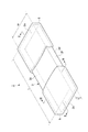
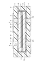
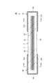
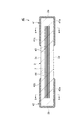
図1は、第1実施形態に係る積層コンデンサを示す斜視図である。図2は、図1に示す積層コンデンサのII−II線での断面構成を示す図である。図3は、図1に示す積層コンデンサのIII−III線での断面構成を示す図である。図4は、図1に示す積層コンデンサの素体の分解斜視図である。
[First Embodiment]
FIG. 1 is a perspective view showing the multilayer capacitor in accordance with the first embodiment. FIG. 2 is a diagram showing a cross-sectional configuration of the multilayer capacitor shown in FIG. 1 taken along line II-II. 3 is a diagram showing a cross-sectional configuration of the multilayer capacitor shown in FIG. 1 taken along the line III-III. 4 is an exploded perspective view of an element body of the multilayer capacitor shown in FIG.

図1に示すように、積層コンデンサ1は、略直方体形状に構成された素体2と、素体2内に配置された第1及び第2内部電極3,4と、素体2の両端部側に配置された第1及び第2端子電極5,6と、を備えている。積層コンデンサ1は、例えば、長さLが0.4mm〜1.6mm程度に設定され、幅Wが0.2mm〜0.8mm程度に設定され、高さHが0.10mm〜035mm程度に設定されている。積層コンデンサ1は、いわゆる低背型コンデンサとして構成されている。   As shown in FIG. 1, the multilayer capacitor 1 includes an element body 2 configured in a substantially rectangular parallelepiped shape, first and second internal electrodes 3 and 4 disposed in the element body 2, and both end portions of the element body 2. First and second terminal electrodes 5 and 6 arranged on the side. For example, the multilayer capacitor 1 has a length L set to about 0.4 mm to 1.6 mm, a width W set to about 0.2 mm to 0.8 mm, and a height H set to about 0.10 mm to 035 mm. Has been. The multilayer capacitor 1 is configured as a so-called low profile capacitor.

素体2は、素体2の長手方向に向かい合って互いに平行をなす一対の第1及び第2端面2a,2bと、第1及び第2端面2a,2b間を連結するように伸び且つ互いに対向する一対の第1及び第2主面2c,2dと、第1及び第2主面2c,2dを連結するように伸び且つ互いに対向する一対の第1及び第2側面2e,2fと、を有する。素体2は、第1及び第2主面2c,2dの間の寸法が、第1及び第2端面2a,2bの間の寸法、及び、第1及び第2側面2e,2fの間の寸法よりも小さい。   The element body 2 extends so as to connect the pair of first and second end faces 2a, 2b facing the longitudinal direction of the element body 2 and parallel to each other, and the first and second end faces 2a, 2b and facing each other. A pair of first and second main surfaces 2c, 2d and a pair of first and second side surfaces 2e, 2f extending to connect the first and second main surfaces 2c, 2d and facing each other. . The element body 2 has a dimension between the first and second main faces 2c, 2d, a dimension between the first and second end faces 2a, 2b, and a dimension between the first and second side faces 2e, 2f. Smaller than.

素体2は、図4に示すように、複数の長方形板状の誘電体層7と、複数(ここではそれぞれ3つ)の第1内部電極3及び第2内部電極4とが積層された積層体として構成されている。第1内部電極3と第2内部電極4とは、素体2内において誘電体層7の積層方向、すなわち素体2の第1主面2cと第2主面2dとが対向する方向に沿ってそれぞれ一層ずつ配置されている。第1内部電極3と第2内部電極4とは、少なくとも一層の誘電体層7を挟むように対向配置されている。実際の積層コンデンサ1では、複数の誘電体層7は、互いの間の境界が視認できない程度に一体化されている。   As shown in FIG. 4, the element body 2 is a laminate in which a plurality of rectangular plate-like dielectric layers 7 and a plurality of (here, three each) first and second internal electrodes 3 and 4 are laminated. It is structured as a body. The first internal electrode 3 and the second internal electrode 4 are arranged in the element body 2 in the stacking direction of the dielectric layers 7, that is, along the direction in which the first main surface 2c and the second main surface 2d of the element body 2 face each other. Are arranged one by one. The first internal electrode 3 and the second internal electrode 4 are disposed so as to face each other with at least one dielectric layer 7 interposed therebetween. In the actual multilayer capacitor 1, the plurality of dielectric layers 7 are integrated to such an extent that the boundary between them cannot be visually recognized.

第1内部電極3は、主電極部3aと、引き出し部3bと、を有している。主電極部3aは、第2内部電極4(主電極部4a)と対向配置されている。主電極部3aは、略矩形形状を呈している。引き出し部3bは、主電極部3aから第1端子電極5の配置された素体2の第1端面2aに伸び、第1端面2aに露出して第1端子電極5(第1焼付電極層5a)と直接的に接続されている。これにより、第1内部電極3と第1端子電極5とは、電気的に接続されることとなる。引き出し部3bは、主電極部3aと同等の幅を有している。これにより、第1内部電極3は、全体として略矩形形状を呈している。   The first internal electrode 3 has a main electrode portion 3a and a lead portion 3b. The main electrode portion 3a is disposed opposite to the second internal electrode 4 (main electrode portion 4a). The main electrode portion 3a has a substantially rectangular shape. The lead portion 3b extends from the main electrode portion 3a to the first end surface 2a of the element body 2 on which the first terminal electrode 5 is disposed, and is exposed to the first end surface 2a to be exposed to the first terminal electrode 5 (first baking electrode layer 5a). ) And directly connected. Thereby, the 1st internal electrode 3 and the 1st terminal electrode 5 will be electrically connected. The lead portion 3b has the same width as the main electrode portion 3a. Thereby, the 1st internal electrode 3 is exhibiting the substantially rectangular shape as a whole.

第2内部電極4は、主電極部4aと、引き出し部4bと、を有している。主電極部4aは、第1内部電極3(主電極部3a)と対向配置されている。主電極部4aは、略矩形形状を呈している。引き出し部4bは、主電極部4aから第2端子電極6の配置された素体2の第2端面2bに伸び、第2端面2bに露出して第2端子電極6(第1焼付電極層6a)と直接的に接続されている。これにより、第2内部電極4と第2端子電極6とは、電気的に接続されることとなる。引き出し部4bは、主電極部4aと同等の幅を有している。これにより、第2内部電極4は、全体として略矩形形状を呈している。   The second internal electrode 4 has a main electrode portion 4a and a lead portion 4b. The main electrode portion 4a is disposed to face the first internal electrode 3 (main electrode portion 3a). The main electrode portion 4a has a substantially rectangular shape. The lead portion 4b extends from the main electrode portion 4a to the second end face 2b of the element body 2 on which the second terminal electrode 6 is disposed, and is exposed to the second end face 2b to be exposed to the second terminal electrode 6 (first baking electrode layer 6a). ) And directly connected. Thereby, the 2nd internal electrode 4 and the 2nd terminal electrode 6 will be electrically connected. The lead portion 4b has the same width as the main electrode portion 4a. Thereby, the 2nd internal electrode 4 is exhibiting the substantially rectangular shape as a whole.

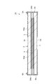
図2に示すように、積層コンデンサ1の素体2において、最上部(第1主面2cに最も近い位置)に配置された第1内部電極3と、最下部(第2主面2dに最も近い位置)に配置された第1内部電極3との間の内層寸法を「D1」とする。また、素体2において、素体2の第1主面2cを構成する誘電体層7の最上層(保護層)と、最上部に配置された第1内部電極3との間の外層寸法を「D2」とする。素体2における外層寸法D2の部分は、複数の誘電体層7が積層されて構成されている。素体2の主面2dを構成する誘電体層7の最下層と、最下部に配置された第1内部電極3との間の外層寸法を「D3」とする。素体2における外層寸法D3の部分は、複数の誘電体層7が積層されて構成されている。   As shown in FIG. 2, in the element body 2 of the multilayer capacitor 1, the first internal electrode 3 disposed at the uppermost portion (position closest to the first main surface 2c) and the lowermost portion (most at the second main surface 2d). The inner layer dimension between the first inner electrode 3 and the first inner electrode 3 disposed at a close position is “D1”. In the element body 2, the outer layer dimension between the uppermost layer (protective layer) of the dielectric layer 7 constituting the first main surface 2 c of the element body 2 and the first inner electrode 3 disposed at the uppermost part is set. “D2”. A portion having the outer layer dimension D2 in the element body 2 is formed by laminating a plurality of dielectric layers 7. The outer layer dimension between the lowermost layer of the dielectric layer 7 constituting the main surface 2d of the element body 2 and the first inner electrode 3 disposed at the lowermost part is defined as “D3”. A portion having the outer layer dimension D3 in the element body 2 is formed by laminating a plurality of dielectric layers 7.

積層コンデンサ1の素体2では、内層寸法D1と外層寸法D2及び外層寸法D3とが以下の関係を満たしている。
D1≒D2,D3
すなわち、内層寸法D1と外層寸法D2,D3とは略同等であり、内層の厚みと、それを挟む一対の外層の厚みとは略同等である。なお、ここで言う略同等とは、例えば5μm程度の誤差を含む。
In the element body 2 of the multilayer capacitor 1, the inner layer dimension D1, the outer layer dimension D2, and the outer layer dimension D3 satisfy the following relationship.
D1 ≒ D2, D3
That is, the inner layer dimension D1 is substantially equal to the outer layer dimensions D2 and D3, and the thickness of the inner layer is approximately equal to the thickness of the pair of outer layers sandwiching the inner layer dimension. Note that “substantially equivalent” here includes an error of about 5 μm, for example.

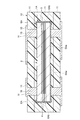
第1端子電極5は、第1端面2a、第2主面2c,2d、及び、第1及び第2側面2e,2fを覆うように配置されている。第1端子電極5は、第1端面2a、第1及び第2主面2c,2d、及び、第1及び第2側面2e,2fにわたって連続して配置されている。第1端子電極5は、第1焼付電極層5aと、第2焼付電極層5bと、めっき層5cと、を有している。   The first terminal electrode 5 is disposed so as to cover the first end surface 2a, the second main surfaces 2c, 2d, and the first and second side surfaces 2e, 2f. The first terminal electrode 5 is continuously arranged over the first end surface 2a, the first and second main surfaces 2c, 2d, and the first and second side surfaces 2e, 2f. The first terminal electrode 5 includes a first baked electrode layer 5a, a second baked electrode layer 5b, and a plating layer 5c.

第1焼付電極層5aは、内部電極3の引き出し部3bが引き出される素体2の第1端面2aと、第1及び第2主面2c,2d、及び、第1及び第2側面2e,2fとに配置されている。第2主面2c,2d、及び、第1及び第2側面2e,2fに配置された第1焼付電極層5aは、第2端面2b側に延在している。第1焼付電極層5aは、金属(例えば、Cu,Ni,Ag、Pd、Au、又はPtなど)を含有する導電性ペースト、あるいは金属とガラス成分(例えば、ホウケイ酸ガラスなど)とを含有する導電性ペーストを例えばディップ工法により素体2に付与し、その導電性ペーストを所定の温度で焼き付けて形成されている。第1焼付電極層5aのガラス成分の含有比率は、例えば0〜5%、好ましくは1〜5%である。   The first baked electrode layer 5a includes the first end face 2a of the element body 2 from which the lead portion 3b of the internal electrode 3 is drawn, the first and second main faces 2c and 2d, and the first and second side faces 2e and 2f. And is arranged. The 1st baking electrode layer 5a arrange | positioned at 2nd main surface 2c, 2d and 1st and 2nd side surface 2e, 2f is extended to the 2nd end surface 2b side. The first baked electrode layer 5a contains a conductive paste containing a metal (for example, Cu, Ni, Ag, Pd, Au, or Pt), or a metal and a glass component (for example, borosilicate glass). The conductive paste is formed by applying the conductive paste to the element body 2 by, for example, a dip method, and baking the conductive paste at a predetermined temperature. The content ratio of the glass component of the first baking electrode layer 5a is, for example, 0 to 5%, preferably 1 to 5%.

第2焼付電極層5bは、第1焼付電極層5a上に配置されている。第2焼付電極層5bは、第1焼付電極層5a上において、素体2の第1端面2aに対応する位置と、第1及び第2主面2c,2d、及び、第1及び第2側面2e,2fに対応する位置の縁部とに配置されている。第1及び第2主面2c,2d、及び、第1及び第2側面2e,2fに配置された第2焼付電極層5bの長さ寸法は、第1焼付電極層5aの長さ寸法よりも小さい。   The second baked electrode layer 5b is disposed on the first baked electrode layer 5a. The second baked electrode layer 5b includes a position corresponding to the first end surface 2a of the element body 2, the first and second main surfaces 2c and 2d, and the first and second side surfaces on the first baked electrode layer 5a. It is arrange | positioned at the edge part of the position corresponding to 2e and 2f. The length dimension of the 2nd baking electrode layer 5b arrange | positioned at the 1st and 2nd main surface 2c, 2d and the 1st and 2nd side surface 2e, 2f is longer than the length dimension of the 1st baking electrode layer 5a. small.

第2焼付電極層5bは、金属とガラス成分とを含有する導電性ペーストを例えばディップ工法により第1焼付電極層5a上に付与し、その導電性ペーストを所定の温度で焼き付けて形成されている。第2焼付電極層5bのガラス成分の含有比率は、例えば5〜10%である。すなわち、第1焼付電極層5aのガラス成分の含有比率は、第2焼付電極層5bのガラス成分の含有比率よりも低い。   The second baking electrode layer 5b is formed by applying a conductive paste containing a metal and a glass component onto the first baking electrode layer 5a by, for example, a dip method, and baking the conductive paste at a predetermined temperature. . The content ratio of the glass component of the second baked electrode layer 5b is, for example, 5 to 10%. That is, the content ratio of the glass component of the first baking electrode layer 5a is lower than the content ratio of the glass component of the second baking electrode layer 5b.

めっき層5cは、第1焼付電極層5a及び第2焼付電極層5bの全体を覆って配置されている。めっき層5cは、例えば、Cuめっき、Niめっき、Snめっきなどの単層構造又はこれらを組み合わせた多層構造である。また、最外層は、Snめっき、もしくは、Cuめっきであることが好ましい。   The plating layer 5c is disposed so as to cover the entire first baking electrode layer 5a and the second baking electrode layer 5b. The plating layer 5c has, for example, a single layer structure such as Cu plating, Ni plating, Sn plating, or a multilayer structure in which these are combined. The outermost layer is preferably Sn plating or Cu plating.

第2端子電極6は、第2端面2b、第1及び第2主面2c,2d、及び、第1及び第2側面2e,2fを覆うように配置されている。第2端子電極6は、第2端面2b、第1及び第2主面2c,2d、及び、第1及び第2側面2e,2fにわたって連続して配置されている。図2に示す第1端子電極5と第2端子電極6との離間距離Gは、図2に示す第1及び第2端子電極5,6の第1及び第2端面2a,2bの対向方向の長さ(幅)H1、及び、図3に示す第1及び第2端子電極5,6の第1及び第2側面2e,2fの対向方向の長さ(幅)H2よりも小さい。   The second terminal electrode 6 is disposed so as to cover the second end face 2b, the first and second main faces 2c, 2d, and the first and second side faces 2e, 2f. The second terminal electrode 6 is continuously arranged over the second end surface 2b, the first and second main surfaces 2c, 2d, and the first and second side surfaces 2e, 2f. The separation distance G between the first terminal electrode 5 and the second terminal electrode 6 shown in FIG. 2 is in the direction opposite to the first and second end faces 2a and 2b of the first and second terminal electrodes 5 and 6 shown in FIG. It is smaller than the length (width) H1 and the length (width) H2 of the first and second terminal electrodes 5, 6 shown in FIG. 3 in the opposing direction of the first and second side surfaces 2e, 2f.

第2端子電極6は、第1焼付電極層6aと、第2焼付電極層6bと、めっき層6cと、を有している。第1焼付電極層6aは、内部電極4の引き出し部4bが引き出される素体2の第1端面2bと、第1及び第2主面2c,2d、及び、第1及び第2側面2e,2fとに配置されている。第1及び第2主面2c,2d、及び、第1及び第2側面2e,2fに配置された第1焼付電極層6aは、第2端面2a側に延在している。第1焼付電極層6aは、第1焼付電極層5aと同様に形成されている。   The second terminal electrode 6 includes a first baking electrode layer 6a, a second baking electrode layer 6b, and a plating layer 6c. The first baked electrode layer 6a includes the first end face 2b of the element body 2 from which the lead portion 4b of the internal electrode 4 is drawn, the first and second main faces 2c and 2d, and the first and second side faces 2e and 2f. And is arranged. The first and second main surfaces 2c and 2d and the first baked electrode layer 6a disposed on the first and second side surfaces 2e and 2f extend to the second end surface 2a side. The first baked electrode layer 6a is formed in the same manner as the first baked electrode layer 5a.

第2焼付電極層6bは、第1焼付電極層6a上に配置されている。第2焼付電極層6bは、第1焼付電極層6a上において、素体2の第1端面2bに対応する位置と、第1及び第2主面2c,2d、及び、第1及び第2側面2e,2fに対応する位置の縁部とに配置されている。第1及び第2主面2c,2d、及び、第1及び第2側面2e,2fに配置された第2焼付電極層6bの長さ寸法は、第1焼付電極層6aの長さ寸法よりも小さい。第2焼付電極層6bは、第1焼付電極層6bと同様に形成されている。第1焼付電極層6aのガラス成分の含有比率は、第2焼付電極層6bのガラス成分の含有比率よりも低い。   The second baked electrode layer 6b is disposed on the first baked electrode layer 6a. The second baked electrode layer 6b includes a position corresponding to the first end surface 2b of the element body 2, the first and second main surfaces 2c, 2d, and the first and second side surfaces on the first baked electrode layer 6a. It is arrange | positioned at the edge part of the position corresponding to 2e and 2f. The length dimension of the 2nd baking electrode layer 6b arrange | positioned at the 1st and 2nd main surface 2c, 2d and the 1st and 2nd side surface 2e, 2f is larger than the length dimension of the 1st baking electrode layer 6a. small. The second baked electrode layer 6b is formed in the same manner as the first baked electrode layer 6b. The content ratio of the glass component of the 1st baking electrode layer 6a is lower than the content ratio of the glass component of the 2nd baking electrode layer 6b.

めっき層6cは、第1焼付電極層6a及び第2焼付電極層6bの全体を覆って配置されている。めっき層6cは、例えば、Cuめっき、Niめっき、Snめっきなどの単層構造又はこれらを組み合わせた多層構造である。   The plating layer 6c is disposed so as to cover the entire first and second baking electrode layers 6a and 6b. The plating layer 6c has, for example, a single layer structure such as Cu plating, Ni plating, Sn plating, or a multilayer structure in which these are combined.

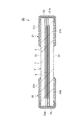
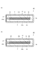
図5は、図1に示す積層コンデンサの実装構造の断面構成を示す図である。図5に示すように、積層コンデンサ1は、基板(回路基板)10に埋め込まれて実装される。基板10は、絶縁性の複数の樹脂シート11が積層されて構成されている。積層コンデンサ1は、基板10の表面に形成された電極13,14とビア導体15,16により電気的に接続されている。   FIG. 5 is a diagram showing a cross-sectional configuration of the multilayer capacitor mounting structure shown in FIG. As shown in FIG. 5, the multilayer capacitor 1 is embedded and mounted in a substrate (circuit board) 10. The substrate 10 is configured by laminating a plurality of insulating resin sheets 11. The multilayer capacitor 1 is electrically connected to electrodes 13 and 14 formed on the surface of the substrate 10 and via conductors 15 and 16.

積層コンデンサ1の実装構造では、基板10に積層コンデンサ1を埋め込んだ後、レーザでビアホールHを形成し、そのビアホールHに無電解めっきでビア導体15,16が形成される。積層コンデンサ1の実装構造では、ビア導体15,16が形成された後、ビア導体15,16と物理的且つ電気的に接続されるように基板10上に電極13,14が形成される。   In the mounting structure of the multilayer capacitor 1, after the multilayer capacitor 1 is embedded in the substrate 10, a via hole H is formed by a laser, and via conductors 15 and 16 are formed in the via hole H by electroless plating. In the multilayer capacitor 1 mounting structure, after the via conductors 15 and 16 are formed, electrodes 13 and 14 are formed on the substrate 10 so as to be physically and electrically connected to the via conductors 15 and 16.

第1端子電極5には、ビア導体15が物理的且つ電気的に接続されている。このとき、第1端子電極5が素体2の主面2cに配置されているため、第1端子電極5とビア導体15との接続を確実に行うことができる。これにより、第1端子電極5と電極13とが電気的に接続されている。第2端子電極6には、ビア導体16が物理的且つ電気的に接続されている。このとき、第2端子電極6が素体2の主面2cに配置されているため、第2端子電極6とビア導体16との接続を確実に行うことができる。これにより、第2端子電極6と電極14とが電気的に接続されている。   A via conductor 15 is physically and electrically connected to the first terminal electrode 5. At this time, since the first terminal electrode 5 is disposed on the main surface 2c of the element body 2, the first terminal electrode 5 and the via conductor 15 can be reliably connected. Thereby, the 1st terminal electrode 5 and the electrode 13 are electrically connected. A via conductor 16 is physically and electrically connected to the second terminal electrode 6. At this time, since the second terminal electrode 6 is disposed on the main surface 2c of the element body 2, the connection between the second terminal electrode 6 and the via conductor 16 can be reliably performed. Thereby, the 2nd terminal electrode 6 and the electrode 14 are electrically connected.

以上説明したように、本実施形態の積層コンデンサ1では、第1焼付電極層5a,6aのガラス成分の含有比率は、第2焼付電極層5b,6bのガラス成分の含有比率よりも低い。これにより、積層コンデンサ1では、第1焼付電極層5a,5bの金属の含有比率が比較的高いため、第1及び第2端子電極5,6と第1及び第2内部電極3,4との接続性を維持できる。また、積層コンデンサ1では、第2焼付電極層5b,6bのガラス成分の含有比率が比較的高いため、素体2や第1焼付電極層5a,6aとの密着性が確保される。したがって、第1及び第2端子電極5,6の密着性の向上が図れる。   As described above, in the multilayer capacitor 1 of the present embodiment, the glass component content ratio of the first baking electrode layers 5a and 6a is lower than the glass component content ratio of the second baking electrode layers 5b and 6b. Thereby, in the multilayer capacitor 1, since the metal content ratio of the first baking electrode layers 5a and 5b is relatively high, the first and second terminal electrodes 5 and 6 and the first and second internal electrodes 3 and 4 Connectivity can be maintained. Further, in the multilayer capacitor 1, since the glass component content ratio of the second baking electrode layers 5b and 6b is relatively high, adhesion with the element body 2 and the first baking electrode layers 5a and 6a is ensured. Therefore, the adhesion between the first and second terminal electrodes 5 and 6 can be improved.

本実施形態の積層コンデンサ1では、第1焼付電極層5a,6aは、素体2の第1、第2端面2a,2b、第1及び第2主面2c,2d、及び、第1及び第2側面2e,2fに配置されており、第2焼付電極層5b,6bは、素体2の第1、第2端面2a,2b側の縁部に配置されている。このような構成により、積層コンデンサ1では、第1及び第2主面2c,2dに第1焼付電極層5a,5bが配置されるため、第1及び第2端子電極5,6の第1及び第2主面2c,2d側の平滑性を確保できる。また、積層コンデンサ1では、素体2の第1及び第2主面2c,2dに第2焼付電極層5b,6bがほとんど配置されないため、第1及び第2端子電極5,6の第1及び第2主面2c,2d側の厚みを小さくできる。   In the multilayer capacitor 1 of the present embodiment, the first baked electrode layers 5a and 6a include the first and second end surfaces 2a and 2b, the first and second main surfaces 2c and 2d, and the first and second The second baked electrode layers 5b and 6b are disposed on the edge portions of the element body 2 on the first and second end surfaces 2a and 2b side. With such a configuration, in the multilayer capacitor 1, the first baking electrode layers 5 a and 5 b are disposed on the first and second main surfaces 2 c and 2 d, so that the first and second terminal electrodes 5 and 6 have the first and second terminal electrodes 5 and 6. Smoothness on the second main surfaces 2c and 2d side can be ensured. In the multilayer capacitor 1, since the second baking electrode layers 5 b and 6 b are hardly arranged on the first and second main surfaces 2 c and 2 d of the element body 2, the first and second terminal electrodes 5 and 6 have the first and second terminal electrodes 5 and 6. The thickness on the second main surface 2c, 2d side can be reduced.

本実施形態の積層コンデンサ1では、第1及び第2主面2c,2dに配置される第1及び第2端子電極5,6の幅H1,H2は,第1端子電極5と第2端子電極6との離間距離Gよりも大きい。これにより、積層コンデンサ1では、第1及び第2端子電極5,6の面積が確保されている。そのため、積層コンデンサ1では、基板10に実装する際に、ビア導体15,16との接触領域を大きくできるため、ビア導体15,16との接続をより確実に行うことができる。   In the multilayer capacitor 1 of the present embodiment, the widths H1 and H2 of the first and second terminal electrodes 5 and 6 disposed on the first and second main surfaces 2c and 2d are the first terminal electrode 5 and the second terminal electrode. 6 is larger than the separation distance G. Thereby, in the multilayer capacitor 1, the area of the 1st and 2nd terminal electrodes 5 and 6 is ensured. Therefore, when the multilayer capacitor 1 is mounted on the substrate 10, the contact area with the via conductors 15 and 16 can be increased, so that the connection with the via conductors 15 and 16 can be more reliably performed.

本実施形態の積層コンデンサ1では、D1≒D2,D3の関係を満たしている。これにより、積層コンデンサ1では、第1内部電極3と第1及び第2主面2c,2dとの間の厚みを比較的大きくしているため、この厚み部分が保護層として機能し、積層コンデンサ1において構造欠陥を抑制できる。また、この構成の積層コンデンサ1では、静電容量を確保できる。   In the multilayer capacitor 1 of the present embodiment, the relationship of D1≈D2, D3 is satisfied. Thereby, in the multilayer capacitor 1, since the thickness between the first internal electrode 3 and the first and second main surfaces 2c, 2d is relatively large, this thickness portion functions as a protective layer, and the multilayer capacitor 1 can suppress structural defects. Further, in the multilayer capacitor 1 having this configuration, a capacitance can be ensured.

上記実施形態では、第1端子電極5及び第2端子電極6がめっき層5c,6cをそれぞれ有している構成を一例に説明したが、めっき層5c,6cは設けられなくてもよい。図6は、積層コンデンサの変形例の断面構成を示す図である。図6に示すように、積層コンデンサ1Aは、素体2と、第1及び第2内部電極3,4と、第1及び第2端子電極5A,6Aと、を備えている。   In the above embodiment, the configuration in which the first terminal electrode 5 and the second terminal electrode 6 have the plating layers 5c and 6c has been described as an example, but the plating layers 5c and 6c may not be provided. FIG. 6 is a diagram illustrating a cross-sectional configuration of a modified example of the multilayer capacitor. As shown in FIG. 6, the multilayer capacitor 1A includes an element body 2, first and second internal electrodes 3 and 4, and first and second terminal electrodes 5A and 6A.

第1端子電極5Aは、第1焼付電極層5Aaと、第2焼付電極層5Abと、を有している。第2端子電極6Aは、第1焼付電極層6Aaと、第2焼付電極層6Abと、を有している。   The first terminal electrode 5A has a first baked electrode layer 5Aa and a second baked electrode layer 5Ab. The second terminal electrode 6A has a first baked electrode layer 6Aa and a second baked electrode layer 6Ab.

図7は、積層コンデンサの実装構造の断面構成を示す図である。図7に示すように、第1端子電極5Aの第1焼付電極層5Aaには、ビア導体15が物理的且つ電気的に直接接続されている。このとき、第1焼付電極層5Aaは、ガラス成分の含有比率が比較的低い(金属の含有量が多い)ため、ビア導体15と確実にめっき等で接続される。第2端子電極6Aの第1焼付電極層6Aaには、ビア導体16が物理的且つ電気的に直接接続されている。このとき、第1焼付電極層6Aaは、ガラス成分の含有比率が比較的低いため、ビア導体16と確実にめっき等で接続される。これにより、第2端子電極6Aと電極14とが電気的に接続されている。   FIG. 7 is a diagram showing a cross-sectional configuration of the multilayer capacitor mounting structure. As shown in FIG. 7, the via conductor 15 is physically and electrically directly connected to the first baked electrode layer 5Aa of the first terminal electrode 5A. At this time, since the content ratio of the glass component is relatively low (the metal content is large), the first baked electrode layer 5Aa is reliably connected to the via conductor 15 by plating or the like. Via conductors 16 are physically and electrically directly connected to the first baked electrode layer 6Aa of the second terminal electrode 6A. At this time, since the content ratio of the glass component is relatively low, the first baking electrode layer 6Aa is reliably connected to the via conductor 16 by plating or the like. Accordingly, the second terminal electrode 6A and the electrode 14 are electrically connected.

[第2実施形態]
続いて、第2実施形態について説明する。図8は、第2実施形態に係る積層コンデンサの断面構成を示す図である。図8に示すように、積層コンデンサ20は、略直方体形状に構成された素体2と、素体2内に配置された第1及び第2内部電極3,4と、素体2の両端部側に配置された第1及び第2端子電極21,22と、を備えている。
[Second Embodiment]
Next, the second embodiment will be described. FIG. 8 is a diagram illustrating a cross-sectional configuration of the multilayer capacitor in accordance with the second embodiment. As shown in FIG. 8, the multilayer capacitor 20 includes an element body 2 configured in a substantially rectangular parallelepiped shape, first and second internal electrodes 3 and 4 disposed in the element body 2, and both end portions of the element body 2. 1 and 2nd terminal electrodes 21 and 22 arranged at the side.

第1端子電極21は、第1焼付電極層21aと、第2焼付電極層21bと、めっき層21cと、を有している。第1焼付電極層21aは、第1内部電極3の引き出し部3bが引き出される第1端面2aと、第1及び第2主面2c,2d、及び、第1及び第2側面2e,2fの縁部とを覆うように配置されている。第1焼付電極層21aは、第1端面2a、第1及び第2主面2c,2d、及び、第1及び第2側面2e,2fにわたって連続して配置されている。   The first terminal electrode 21 includes a first baking electrode layer 21a, a second baking electrode layer 21b, and a plating layer 21c. The first baked electrode layer 21a includes the first end surface 2a from which the lead portion 3b of the first internal electrode 3 is drawn, the edges of the first and second main surfaces 2c and 2d, and the first and second side surfaces 2e and 2f. It arrange | positions so that a part may be covered. The first baked electrode layer 21a is continuously arranged over the first end surface 2a, the first and second main surfaces 2c, 2d, and the first and second side surfaces 2e, 2f.

第1焼付電極層21aは、金属を含有する導電性ペースト、あるいは金属とガラス成分とを含有する導電性ペーストを例えばディップ工法により素体2に付与し、その導電性ペーストを所定の温度で焼き付けて形成されている。第1焼付電極層21aのガラス成分の含有比率は、例えば0〜5%、好ましくは1〜5%である。   For the first baking electrode layer 21a, a conductive paste containing a metal or a conductive paste containing a metal and a glass component is applied to the element body 2 by, for example, a dipping method, and the conductive paste is baked at a predetermined temperature. Is formed. The content ratio of the glass component of the first baking electrode layer 21a is, for example, 0 to 5%, preferably 1 to 5%.

第2焼付電極層21bは、第1焼付電極層21a上に配置されていると共に、素体2の第1及び第2主面2c,2d、及び、第1及び第2側面2e,2f上に配置されている。第2焼付電極層21bは、第1焼付電極層21aを覆うと共に、第2主面2c,2d、及び、第1及び第2側面2e,2fにおいて、第2端面2b側に延在している。第1及び第2主面2c,2d、及び、第1及び第2側面2e,2fに配置された第2焼付電極層21bの長さ寸法は、第1焼付電極層21aの長さ寸法よりも大きい。   The second baked electrode layer 21b is disposed on the first baked electrode layer 21a, and on the first and second main surfaces 2c and 2d and the first and second side surfaces 2e and 2f of the element body 2. Is arranged. The second baked electrode layer 21b covers the first baked electrode layer 21a and extends to the second end surface 2b side in the second main surfaces 2c and 2d and the first and second side surfaces 2e and 2f. . The length dimension of the 2nd baking electrode layer 21b arrange | positioned at the 1st and 2nd main surface 2c, 2d and the 1st and 2nd side surface 2e, 2f is larger than the length dimension of the 1st baking electrode layer 21a. large.

第2焼付電極層21bは、金属とガラス成分とを含有する導電性ペーストを例えばディップ工法により第1焼付電極層21a上及び素体2の第1及び第2主面2c,2d、及び、第1及び第2側面2e,2f上に付与し、その導電性ペーストを所定の温度で焼き付けて形成されている。第2焼付電極層21bのガラス成分の含有比率は、例えば5〜10%である。すなわち、第1焼付電極層21aのガラス成分の含有比率は、第2焼付電極層21bのガラス成分の含有比率よりも低い。   The second baked electrode layer 21b is formed of a conductive paste containing a metal and a glass component, for example, on the first baked electrode layer 21a and the first and second main surfaces 2c, 2d of the element body 2 by the dipping method. The conductive paste is applied onto the first and second side surfaces 2e and 2f, and the conductive paste is baked at a predetermined temperature. The content ratio of the glass component of the second baked electrode layer 21b is, for example, 5 to 10%. That is, the content ratio of the glass component of the first baked electrode layer 21a is lower than the content ratio of the glass component of the second baked electrode layer 21b.

めっき層21cは、第2焼付電極層21bの全体を覆って配置されている。めっき層21cは、例えば、Cuめっき、Niめっき、Snめっきなどの単層構造又はこれらを組み合わせた多層構造である。   The plating layer 21c is disposed so as to cover the entire second baking electrode layer 21b. The plating layer 21c has, for example, a single layer structure such as Cu plating, Ni plating, Sn plating, or a multilayer structure in which these are combined.

第2端子電極22は、第1焼付電極層22aと、第2焼付電極層22bと、めっき層22cと、を有している。第1焼付電極層22aは、第2内部電極4の引き出し部4bが引き出される第1端面2bと、第1及び第2主面2c,2d、及び、第1及び第2側面2e,2fの縁部とを覆うように配置されている。第1焼付電極層22aは、第1焼付電極層22bと同様に形成されている。   The second terminal electrode 22 includes a first baked electrode layer 22a, a second baked electrode layer 22b, and a plating layer 22c. The first baked electrode layer 22a includes the first end face 2b from which the lead portion 4b of the second internal electrode 4 is drawn, the edges of the first and second main faces 2c and 2d, and the first and second side faces 2e and 2f. It arrange | positions so that a part may be covered. The first baked electrode layer 22a is formed in the same manner as the first baked electrode layer 22b.

第2焼付電極層22bは、第1焼付電極層21a上に配置されていると共に、素体2の第1及び第2主面2c,2d、及び、第1及び第2側面2e,2f上に配置されている。第2焼付電極層22bは、第1焼付電極層22aを覆うと共に、第2主面2c,2d、及び、第1及び第2側面2e,2fにおいて、第1端面2a側に延在している。第1及び第2主面2c,2d、及び、第1及び第2側面2e,2fに配置された第2焼付電極層22bの長さ寸法は、第1焼付電極層22aの長さ寸法よりも大きい。第2焼付電極層22bは、第2焼付電極層21bと同様に形成されている。第1焼付電極層22aのガラス成分の含有比率は、第2焼付電極層22bのガラス成分の含有比率よりも低い。   The second baked electrode layer 22b is disposed on the first baked electrode layer 21a, and on the first and second main surfaces 2c and 2d and the first and second side surfaces 2e and 2f of the element body 2. Is arranged. The second baked electrode layer 22b covers the first baked electrode layer 22a, and extends to the first end surface 2a side in the second main surfaces 2c and 2d and the first and second side surfaces 2e and 2f. . The length dimension of the 2nd baking electrode layer 22b arrange | positioned at the 1st and 2nd main surface 2c, 2d and the 1st and 2nd side surface 2e, 2f is larger than the length dimension of the 1st baking electrode layer 22a. large. The second baked electrode layer 22b is formed in the same manner as the second baked electrode layer 21b. The content ratio of the glass component of the first baked electrode layer 22a is lower than the content ratio of the glass component of the second baked electrode layer 22b.

めっき層22cは、第2焼付電極層22bの全体を覆って配置されている。めっき層21cは、例えば、Cuめっき、Niめっき、Snめっきなどの単層構造又はこれらを組み合わせた多層構造である。   The plating layer 22c is disposed so as to cover the entire second baking electrode layer 22b. The plating layer 21c has, for example, a single layer structure such as Cu plating, Ni plating, Sn plating, or a multilayer structure in which these are combined.

図9は、図8に示す積層コンデンサの実装構造の断面構成を示す図である。図9に示すように、積層コンデンサ20は、基板10に埋め込まれて実装される。第1端子電極21には、ビア導体15が物理的且つ電気的に接続されている。このとき、第1端子電極21が素体2の主面2cに配置されているため、第1端子電極21とビア導体15との接続を確実に行うことができる。これにより、第1端子電極21と電極13とが電気的に接続されている。第2端子電極22には、ビア導体16が物理的且つ電気的に接続されている。このとき、第2端子電極22が素体2の主面2cに配置されているため、第2端子電極22とビア導体16との接続を確実に行うことができる。これにより、第2端子電極22と電極14とが電気的に接続されている。   FIG. 9 is a diagram showing a cross-sectional configuration of the multilayer capacitor mounting structure shown in FIG. As shown in FIG. 9, the multilayer capacitor 20 is embedded and mounted in the substrate 10. A via conductor 15 is physically and electrically connected to the first terminal electrode 21. At this time, since the first terminal electrode 21 is disposed on the main surface 2c of the element body 2, the first terminal electrode 21 and the via conductor 15 can be reliably connected. Thereby, the 1st terminal electrode 21 and the electrode 13 are electrically connected. The via conductor 16 is physically and electrically connected to the second terminal electrode 22. At this time, since the second terminal electrode 22 is disposed on the main surface 2c of the element body 2, the connection between the second terminal electrode 22 and the via conductor 16 can be reliably performed. Thereby, the 2nd terminal electrode 22 and the electrode 14 are electrically connected.

本実施形態の積層コンデンサ20では、第1焼付電極層21a,22aは、素体2の第1、第2端面2a,2b側の縁部に配置されており、第2焼付電極層21b,22bは、第1焼付電極層21a,22a上と、第1及び第2主面2c,2d、及び、第1及び第2側面2e,2fとに配置されている。このように、積層コンデンサ20では、素体2の第1及び第2主面2c,2dに第1焼付電極層21a,22aがほとんど配置されないため、第1及び第2端子電極21,22の第1及び第2主面2c,2d側の厚みを小さくできる。また、積層コンデンサ20では、ガラス成分の含有比率が比較的高い第2焼付電極層21b,22bが素体2の第1及び第2主面2c,2dに配置されるため、第1及び第2端子電極21,22の第1及び第2主面2c,2d側(ビア導体15,16とのコンタクト部分)において第1及び第2端子電極21,22と素体2との密着性を確保できる。   In the multilayer capacitor 20 of the present embodiment, the first baked electrode layers 21a and 22a are arranged at the edge portions of the element body 2 on the first and second end faces 2a and 2b side, and the second baked electrode layers 21b and 22b. Are disposed on the first baked electrode layers 21a and 22a, the first and second main surfaces 2c and 2d, and the first and second side surfaces 2e and 2f. Thus, in the multilayer capacitor 20, the first baking electrode layers 21 a and 22 a are hardly arranged on the first and second main surfaces 2 c and 2 d of the element body 2, so that the first and second terminal electrodes 21 and 22 have the first The thickness on the first and second main surfaces 2c, 2d side can be reduced. Further, in the multilayer capacitor 20, since the second baking electrode layers 21b and 22b having a relatively high glass component content ratio are disposed on the first and second main surfaces 2c and 2d of the element body 2, the first and second Adhesion between the first and second terminal electrodes 21 and 22 and the element body 2 can be ensured on the first and second main surfaces 2c and 2d side of the terminal electrodes 21 and 22 (contact portions with the via conductors 15 and 16). .

[第3実施形態]
続いて、第3実施形態について説明する。図10は、第3実施形態に係る積層コンデンサの断面構成を示す図である。図11(a)は、図10に示す積層コンデンサのa−a線での断面構成を示す図であり、図11(b)は、図10に示す積層コンデンサのb−b線での断面構成を示す図である。図12は、図10に示す積層コンデンサの素体の分解斜視図である。
[Third Embodiment]
Subsequently, the third embodiment will be described. FIG. 10 is a diagram illustrating a cross-sectional configuration of the multilayer capacitor in accordance with the third embodiment. 11A is a diagram showing a cross-sectional configuration of the multilayer capacitor shown in FIG. 10 taken along line aa, and FIG. 11B is a cross-sectional configuration of the multilayer capacitor shown in FIG. 10 taken along line bb. FIG. 12 is an exploded perspective view of the multilayer capacitor body shown in FIG.

図10に示すように、積層コンデンサ30は、略直方体形状に構成された素体2と、素体2内に配置された第1及び第2内部電極33,34と、素体2の両端部側に配置された第1及び第2端子電極31,32と、を備えている。   As shown in FIG. 10, the multilayer capacitor 30 includes an element body 2 configured in a substantially rectangular parallelepiped shape, first and second internal electrodes 33 and 34 disposed in the element body 2, and both end portions of the element body 2. And first and second terminal electrodes 31 and 32 arranged on the side.

図12に示すように、第1内部電極33は、主電極部33aと、引き出し部33bと、を有している。主電極部33aは、第2内部電極34(主電極部34a)と対向配置されている。主電極部33aは、略矩形形状を呈している。引き出し部33bは、主電極部33aから第1端子電極31の配置された素体2の第1及び第2側面2e,2fのそれぞれに伸び、第1及び第2側面2e,2fに露出して第1端子電極31(第1焼付電極層31a)と直接的に接続されている。これにより、第1内部電極33と第1端子電極31とは、電気的に接続されることとなる。   As shown in FIG. 12, the first internal electrode 33 has a main electrode portion 33a and a lead portion 33b. The main electrode portion 33a is disposed to face the second internal electrode 34 (main electrode portion 34a). The main electrode portion 33a has a substantially rectangular shape. The lead portion 33b extends from the main electrode portion 33a to the first and second side surfaces 2e and 2f of the element body 2 on which the first terminal electrode 31 is disposed, and is exposed to the first and second side surfaces 2e and 2f. It is directly connected to the first terminal electrode 31 (first baking electrode layer 31a). Thereby, the 1st internal electrode 33 and the 1st terminal electrode 31 will be electrically connected.

第2内部電極34は、主電極部34aと、引き出し部34bと、を有している。主電極部34aは、第1内部電極33(主電極部33a)と対向配置されている。主電極部34aは、略矩形形状を呈している。引き出し部34bは、主電極部34aから第2端子電極32の配置された素体2の第1及び第2側面2e,2fのそれぞれに伸び、第1及び第2側面2e,2fに露出して第2端子電極32(第1焼付電極層32a)と直接的に接続されている。これにより、第2内部電極34と第2端子電極32とは、電気的に接続されることとなる。   The second internal electrode 34 has a main electrode part 34a and a lead part 34b. The main electrode portion 34a is disposed to face the first internal electrode 33 (main electrode portion 33a). The main electrode portion 34a has a substantially rectangular shape. The lead portion 34b extends from the main electrode portion 34a to the first and second side surfaces 2e and 2f of the element body 2 in which the second terminal electrode 32 is disposed, and is exposed to the first and second side surfaces 2e and 2f. It is directly connected to the second terminal electrode 32 (first baking electrode layer 32a). Thereby, the 2nd internal electrode 34 and the 2nd terminal electrode 32 will be electrically connected.

図10及び図11に示すように、第1端子電極31は、第1端面2a、第1及び第2主面2c,2d、及び、第1及び第2側面2e,2fを覆うように配置されている。第1端子電極31は、第1端面2a、第1及び第2主面2c,2d、及び、第1及び第2側面2e,2fにわたって連続して配置されている。第1端子電極31は、第1焼付電極層31aと、第2焼付電極層31bと、めっき層31cと、を有している。   As shown in FIGS. 10 and 11, the first terminal electrode 31 is disposed so as to cover the first end surface 2a, the first and second main surfaces 2c, 2d, and the first and second side surfaces 2e, 2f. ing. The first terminal electrode 31 is continuously arranged over the first end surface 2a, the first and second main surfaces 2c, 2d, and the first and second side surfaces 2e, 2f. The first terminal electrode 31 includes a first baked electrode layer 31a, a second baked electrode layer 31b, and a plating layer 31c.

第1焼付電極層31aは、素体2の第1端面2aと、第1及び第2主面2c,2d、及び、第1内部電極33の引き出し部33bが引き出される第1及び第2側面2e,2fとに配置されている。第1及び第2主面2c,2d、及び、第1及び第2側面2e,2fに配置された第1焼付電極層31aは、第2端面2b側に延在している。第1焼付電極層31aは、金属を含有する導電性ペースト、あるいは金属とガラス成分とを含有する導電性ペーストを例えばディップ工法により素体2に付与し、その導電性ペーストを所定の温度で焼き付けて形成されている。第1焼付電極層31aのガラス成分の含有比率は、例えば0〜5%、好ましくは1〜5%である。   The first baked electrode layer 31a includes first and second side faces 2e from which the first end face 2a of the element body 2, the first and second main faces 2c and 2d, and the lead-out portion 33b of the first internal electrode 33 are drawn out. , 2f. The first and second main surfaces 2c and 2d and the first baked electrode layer 31a disposed on the first and second side surfaces 2e and 2f extend to the second end surface 2b side. The first baking electrode layer 31a is formed by applying a conductive paste containing a metal or a conductive paste containing a metal and a glass component to the element body 2 by, for example, a dipping method, and baking the conductive paste at a predetermined temperature. Is formed. The content ratio of the glass component of the first baked electrode layer 31a is, for example, 0 to 5%, preferably 1 to 5%.

第2焼付電極層31bは、第1焼付電極層31a上に配置されている。第2焼付電極層31bは、第1焼付電極層31a上において、素体2の第1及び第2側面2e,2fに対応する位置に配置されている。なお、第2焼付電極層31bは、素体2の第1主面2cの縁部と第2主面2dの縁部に跨っていてもよい。   The second baked electrode layer 31b is disposed on the first baked electrode layer 31a. The second baked electrode layer 31b is disposed on the first baked electrode layer 31a at positions corresponding to the first and second side surfaces 2e and 2f of the element body 2. The second baked electrode layer 31b may straddle the edge of the first main surface 2c and the edge of the second main surface 2d of the element body 2.

第2焼付電極層31bは、金属とガラス成分とを含有する導電性ペーストを例えば転写により第1焼付電極層31a上に付与し、その導電性ペーストを所定の温度で焼き付けて形成されている。第2焼付電極層31bのガラス成分の含有比率は、例えば5〜10%である。すなわち、第1焼付電極層31aのガラス成分の含有比率は、第2焼付電極層31bのガラス成分の含有比率よりも低い。   The second baked electrode layer 31b is formed by applying a conductive paste containing a metal and a glass component onto the first baked electrode layer 31a by transfer, for example, and baking the conductive paste at a predetermined temperature. The content ratio of the glass component of the second baking electrode layer 31b is, for example, 5 to 10%. That is, the content ratio of the glass component of the first baking electrode layer 31a is lower than the content ratio of the glass component of the second baking electrode layer 31b.

めっき層31cは、第1焼付電極層31a及び第2焼付電極層31bの全体を覆って配置されている。めっき層31cは、例えば、Cuめっき、Niめっき、Snめっきなどの単層構造又はこれらを組み合わせた多層構造である。   The plating layer 31c is disposed so as to cover the entire first baking electrode layer 31a and the second baking electrode layer 31b. The plating layer 31c has, for example, a single layer structure such as Cu plating, Ni plating, or Sn plating, or a multilayer structure combining these.

第2端子電極32は、第2端面2b、第1及び第2主面2c,2d、及び、第1及び第2側面2e,2fを覆うように配置されている。第2端子電極32は、第2端面2b、第1及び第2主面2c,2d、及び、第1及び第2側面2e,2fにわたって連続して配置されている。第2端子電極32は、第1焼付電極層32aと、第2焼付電極層32bと、めっき層32cと、を有している。   The second terminal electrode 32 is disposed so as to cover the second end face 2b, the first and second main faces 2c, 2d, and the first and second side faces 2e, 2f. The second terminal electrode 32 is continuously arranged over the second end face 2b, the first and second main faces 2c, 2d, and the first and second side faces 2e, 2f. The second terminal electrode 32 includes a first baked electrode layer 32a, a second baked electrode layer 32b, and a plating layer 32c.

第1焼付電極層32aは、素体2の第2端面2bと、第1及び第2主面2c,2d、及び、第2内部電極34の引き出し部34bが引き出される第1及び第2側面2e,2fとに配置されている。第1及び第2主面2c,2d、及び、第1及び第2側面2e,2fに配置された第1焼付電極層32aは、第1端面2a側に延在している。第1焼付電極層32aは、第1焼付電極層31aと同様に形成されている。   The first baked electrode layer 32a includes first and second side faces 2e from which the second end face 2b of the element body 2, the first and second main faces 2c and 2d, and the lead-out portion 34b of the second internal electrode 34 are drawn out. , 2f. The 1st and 2nd main surfaces 2c and 2d and the 1st baking electrode layer 32a arrange | positioned at the 1st and 2nd side surfaces 2e and 2f are extended to the 1st end surface 2a side. The first baked electrode layer 32a is formed in the same manner as the first baked electrode layer 31a.

第2焼付電極層32bは、第1焼付電極層32a上に配置されている。第2焼付電極層32bは、第1焼付電極層32a上において、素体2の第1及び第2側面2e,2fに対応する位置に配置されている。なお、第2焼付電極層31bは、素体2の第1主面2cの縁部と第2主面2dの縁部に跨っていてもよい。第2焼付電極層32bは、第2焼付電極層31bと同様に形成されている。第1焼付電極層32aのガラス成分の含有比率は、第2焼付電極層32bのガラス成分の含有比率よりも低い。   The second baked electrode layer 32b is disposed on the first baked electrode layer 32a. The second baked electrode layer 32b is disposed on the first baked electrode layer 32a at positions corresponding to the first and second side surfaces 2e and 2f of the element body 2. The second baked electrode layer 31b may straddle the edge of the first main surface 2c and the edge of the second main surface 2d of the element body 2. The second baked electrode layer 32b is formed in the same manner as the second baked electrode layer 31b. The glass component content ratio of the first baked electrode layer 32a is lower than the glass component content ratio of the second baked electrode layer 32b.

めっき層32cは、第1焼付電極層32a及び第2焼付電極層32bの全体を覆って配置されている。めっき層32cは、例えば、Cuめっき、Niめっき、Snめっきなどの単層構造又はこれらを組み合わせた多層構造である。   The plating layer 32c is disposed so as to cover the entire first baking electrode layer 32a and the second baking electrode layer 32b. The plating layer 32c has, for example, a single layer structure such as Cu plating, Ni plating, or Sn plating, or a multilayer structure combining these.

以上説明したように、本実施形態に係る積層コンデンサ30では、第1及び第2内部電極33,34の引き出し部33b,34bが素体2の第1及び第2側面2e,2fに引き出されている。これにより、積層コンデンサ30では、引き出し部33bと引き出し部34bとの間の距離を小さくすることができるので、低ESLとすることができる。   As described above, in the multilayer capacitor 30 according to this embodiment, the lead portions 33b and 34b of the first and second internal electrodes 33 and 34 are drawn to the first and second side surfaces 2e and 2f of the element body 2. Yes. Thereby, in the multilayer capacitor 30, since the distance between the lead-out part 33b and the lead-out part 34b can be reduced, the ESL can be reduced.

なお、積層コンデンサ30では、第1及び第2端子電極31,32が素体2の第1、第2端面2a,2b、第1及び第2主面2c,2d、及び、第1及び第2側面2e,2fを覆うように配置されているが、端子電極は、第1、第2端面2a,2bには形成されなくてもよいし、第1及び第2主面2c,2dのいずれか一方の主面だけに形成されてもよい。この場合、例えば印刷工法などで端子電極を形成すればよい。   In the multilayer capacitor 30, the first and second terminal electrodes 31 and 32 include the first and second end faces 2 a and 2 b, the first and second main faces 2 c and 2 d, and the first and second end faces of the element body 2. Although arranged so as to cover the side surfaces 2e and 2f, the terminal electrode may not be formed on the first and second end surfaces 2a and 2b, or one of the first and second main surfaces 2c and 2d. It may be formed only on one main surface. In this case, the terminal electrode may be formed by, for example, a printing method.

[第4実施形態]
続いて、第4実施形態について説明する。図13は、第4実施形態に係る積層コンデンサの断面構成を示す図である。図14(a)は、図13に示す積層コンデンサのa−a線での断面構成を示す図であり、図14(b)は、図13に示す積層コンデンサのb−b線での断面構成を示す図である。図15は、図15に示す積層コンデンサの素体の分解斜視図である。
[Fourth Embodiment]
Subsequently, a fourth embodiment will be described. FIG. 13 is a diagram illustrating a cross-sectional configuration of the multilayer capacitor in accordance with the fourth embodiment. 14A is a diagram showing a cross-sectional configuration of the multilayer capacitor shown in FIG. 13 taken along line aa, and FIG. 14B is a cross-sectional configuration of the multilayer capacitor shown in FIG. 13 taken along line bb. FIG. 15 is an exploded perspective view of the multilayer capacitor body shown in FIG.

図13に示すように、積層コンデンサ40は、略直方体形状に構成された素体2と、素体2内に配置された第1及び第2内部電極43,44と、素体2の両端部側に配置された第1及び第2端子電極41,42と、を備えている。   As shown in FIG. 13, the multilayer capacitor 40 includes an element body 2 configured in a substantially rectangular parallelepiped shape, first and second internal electrodes 43 and 44 disposed in the element body 2, and both end portions of the element body 2. First and second terminal electrodes 41 and 42 disposed on the side.

図15に示すように、第1内部電極43は、主電極部43aと、引き出し部43bと、を有している。主電極部43aは、第2内部電極44(主電極部44a)と対向配置されている。主電極部43aは、略矩形形状を呈している。引き出し部43bは、主電極部43aから第1端子電極41の配置された素体2の第2側面2fに伸び、第2側面2fに露出して第1端子電極41(第1焼付電極層41a)と直接的に接続されている。これにより、第1内部電極43と第1端子電極41とは、電気的に接続されることとなる。   As shown in FIG. 15, the first internal electrode 43 includes a main electrode portion 43a and a lead portion 43b. The main electrode portion 43a is disposed to face the second internal electrode 44 (main electrode portion 44a). The main electrode portion 43a has a substantially rectangular shape. The lead portion 43b extends from the main electrode portion 43a to the second side surface 2f of the element body 2 on which the first terminal electrode 41 is disposed, and is exposed to the second side surface 2f to be exposed to the first terminal electrode 41 (first printed electrode layer 41a). ) And directly connected. Thereby, the 1st internal electrode 43 and the 1st terminal electrode 41 will be electrically connected.

第2内部電極44は、主電極部44aと、引き出し部44bと、を有している。主電極部44aは、第1内部電極43(主電極部43a)と対向配置されている。主電極部44aは、略矩形形状を呈している。引き出し部44bは、主電極部44aから第2端子電極42の配置された素体2の第2側面2fに伸び、第2側面2fに露出して第2端子電極42(第1焼付電極層42a)と直接的に接続されている。これにより、第2内部電極44と第2端子電極42とは、電気的に接続されることとなる。   The second internal electrode 44 has a main electrode portion 44a and a lead portion 44b. The main electrode portion 44a is disposed to face the first internal electrode 43 (main electrode portion 43a). The main electrode portion 44a has a substantially rectangular shape. The lead portion 44b extends from the main electrode portion 44a to the second side surface 2f of the element body 2 on which the second terminal electrode 42 is disposed, and is exposed to the second side surface 2f to expose the second terminal electrode 42 (first baking electrode layer 42a). ) And directly connected. Thereby, the 2nd internal electrode 44 and the 2nd terminal electrode 42 will be electrically connected.

図13及び図14に示すように、第1端子電極41は、第1端面2a、第1及び第2主面2c,2d、及び、第1及び第2側面2e,2fを覆うように配置されている。第1端子電極41は、第1端面2a、第1及び第2主面2c,2d、及び、第1及び第2側面2e,2fにわたって連続して配置されている。第1端子電極41は、第1焼付電極層41aと、第2焼付電極層41bと、めっき層41cと、を有している。   As shown in FIGS. 13 and 14, the first terminal electrode 41 is disposed so as to cover the first end face 2a, the first and second main faces 2c, 2d, and the first and second side faces 2e, 2f. ing. The first terminal electrode 41 is continuously arranged over the first end surface 2a, the first and second main surfaces 2c, 2d, and the first and second side surfaces 2e, 2f. The first terminal electrode 41 includes a first baking electrode layer 41a, a second baking electrode layer 41b, and a plating layer 41c.

第1焼付電極層41aは、素体2の第1端面2aと、第1及び第2主面2c,2d、及び、第1及び第2側面2e,2fとに配置されている。第1及び第2主面2c,2d、及び、第1及び第2側面2e,2fに配置された第1焼付電極層41aは、第2端面2b側に延在している。第1焼付電極層41aは、金属を含有する導電性ペースト、あるいは金属とガラス成分とを含有する導電性ペーストを例えばディップ工法により素体2に付与し、その導電性ペーストを所定の温度で焼き付けて形成されている。第1焼付電極層41aのガラス成分の含有比率は、例えば0〜5%、好ましくは1〜5%である。   The first baked electrode layer 41a is disposed on the first end face 2a of the element body 2, the first and second main faces 2c, 2d, and the first and second side faces 2e, 2f. The first and second main surfaces 2c and 2d and the first baked electrode layer 41a disposed on the first and second side surfaces 2e and 2f extend to the second end surface 2b side. For the first baking electrode layer 41a, a conductive paste containing a metal or a conductive paste containing a metal and a glass component is applied to the element body 2 by, for example, a dipping method, and the conductive paste is baked at a predetermined temperature. Is formed. The content ratio of the glass component of the first baking electrode layer 41a is, for example, 0 to 5%, preferably 1 to 5%.

第2焼付電極層41bは、第1焼付電極層41a上に配置されている。第2焼付電極層41bは、第1焼付電極層41a上において、素体2の第2側面2fに対応する位置に配置されている。   The second baked electrode layer 41b is disposed on the first baked electrode layer 41a. The second baked electrode layer 41b is disposed at a position corresponding to the second side surface 2f of the element body 2 on the first baked electrode layer 41a.

第2焼付電極層41bは、金属とガラス成分とを含有する導電性ペーストを例えば転写により第1焼付電極層41a上に付与し、その導電性ペーストを所定の温度で焼き付けて形成されている。第2焼付電極層41bのガラス含有比率は、例えば5〜10%である。すなわち、第1焼付電極層41aのガラス成分の含有比率は、第2焼付電極層41bのガラス成分の含有比率よりも低い。   The second baked electrode layer 41b is formed by applying a conductive paste containing a metal and a glass component onto the first baked electrode layer 41a by transfer, for example, and baking the conductive paste at a predetermined temperature. The glass content ratio of the second baked electrode layer 41b is, for example, 5 to 10%. That is, the content ratio of the glass component of the first baking electrode layer 41a is lower than the content ratio of the glass component of the second baking electrode layer 41b.

めっき層41cは、第1焼付電極層41a及び第2焼付電極層41bの全体を覆って配置されている。めっき層41cは、例えば、Cuめっき、Niめっき、Snめっきなどの単層構造又はこれらを組み合わせた多層構造である。   The plating layer 41c is disposed so as to cover the entire first baking electrode layer 41a and the second baking electrode layer 41b. The plating layer 41c has, for example, a single layer structure such as Cu plating, Ni plating, or Sn plating, or a multilayer structure combining these.

第2端子電極42は、第2端面2b、第1及び第2主面2c,2d、及び、第1及び第2側面2e,2fを覆うように配置されている。第2端子電極42は、第2端面2b、第1及び第2主面2c,2d、及び、第1及び第2側面2e,2fにわたって連続して配置されている。第2端子電極42は、第1焼付電極層42aと、第2焼付電極層42bと、めっき層42cと、を有している。   The second terminal electrode 42 is disposed so as to cover the second end face 2b, the first and second main faces 2c, 2d, and the first and second side faces 2e, 2f. The second terminal electrode 42 is continuously arranged over the second end surface 2b, the first and second main surfaces 2c, 2d, and the first and second side surfaces 2e, 2f. The second terminal electrode 42 includes a first baked electrode layer 42a, a second baked electrode layer 42b, and a plating layer 42c.

第1焼付電極層42aは、素体2の第2端面2bと、第1及び第2主面2c,2d、及び、第1及び第2側面2e,2fとに配置されている。第1及び第2主面2c,2d、及び、第1及び第2側面2e,2fに配置された第1焼付電極層42aは、第1端面2a側に延在している。第1焼付電極層42aは、第1焼付電極層41aと同様に形成されている。   The first baking electrode layer 42a is disposed on the second end surface 2b of the element body 2, the first and second main surfaces 2c and 2d, and the first and second side surfaces 2e and 2f. The first and second main surfaces 2c and 2d and the first baked electrode layers 42a disposed on the first and second side surfaces 2e and 2f extend to the first end surface 2a side. The first baked electrode layer 42a is formed in the same manner as the first baked electrode layer 41a.

第2焼付電極層42bは、第1焼付電極層42a上に配置されている。第2焼付電極層42bは、第1焼付電極層41a上において、素体2の第2側面2fに対応する位置に配置されている。第2焼付電極層42bは、第2焼付電極層41bと同様に形成されている。第1焼付電極層42aのガラス成分の含有比率は、第2焼付電極層42bのガラス成分の含有比率よりも低い。   The second baked electrode layer 42b is disposed on the first baked electrode layer 42a. The second baked electrode layer 42b is disposed at a position corresponding to the second side surface 2f of the element body 2 on the first baked electrode layer 41a. The second baked electrode layer 42b is formed in the same manner as the second baked electrode layer 41b. The content ratio of the glass component of the first baked electrode layer 42a is lower than the content ratio of the glass component of the second baked electrode layer 42b.

めっき層42cは、第1焼付電極層42a及び第2焼付電極層42bの全体を覆って配置されている。めっき層42cは、例えば、Cuめっき、Niめっき、Snめっきなどの単層構造又はこれらを組み合わせた多層構造である。   The plating layer 42c is disposed so as to cover the entire first baking electrode layer 42a and the second baking electrode layer 42b. The plating layer 42c has, for example, a single layer structure such as Cu plating, Ni plating, Sn plating, or a multilayer structure in which these are combined.

以上説明したように、本実施形態に係る積層コンデンサ40では、第1及び第2内部電極43,44の引き出し部43b,44bが素体2の第2側面2fに引き出されている。これにより、積層コンデンサ30では、引き出し部43bと引き出し部44bとの間の距離を小さくすることができるので、低ESLとすることができる。   As described above, in the multilayer capacitor 40 according to this embodiment, the lead portions 43 b and 44 b of the first and second internal electrodes 43 and 44 are drawn to the second side surface 2 f of the element body 2. Thereby, in the multilayer capacitor 30, since the distance between the lead part 43b and the lead part 44b can be reduced, the ESL can be reduced.

なお、積層コンデンサ40では、第1及び第2端子電極41,42が素体2の第1、第2端面2a,2b、第1及び第2主面2c,2d、及び、第1及び第2側面2e,2fを覆うように配置されているが、端子電極は、第1、第2端面2a,2bには形成されなくてもよいし、第1及び第2主面2c,2dのいずれか一方の主面だけに形成されてもよい。この場合、例えば印刷工法などで端子電極を形成すればよい。   In the multilayer capacitor 40, the first and second terminal electrodes 41 and 42 include the first and second end faces 2 a and 2 b, the first and second main faces 2 c and 2 d, and the first and second end faces of the element body 2. Although arranged so as to cover the side surfaces 2e and 2f, the terminal electrode may not be formed on the first and second end surfaces 2a and 2b, or one of the first and second main surfaces 2c and 2d. It may be formed only on one main surface. In this case, the terminal electrode may be formed by, for example, a printing method.

[第5実施形態]
続いて、第5実施形態について説明する。図16は、第5実施形態に係る積層コンデンサの断面構成を示す図である。図17(a)は、図16に示す積層コンデンサのa−a線での断面構成を示す図であり、図17(b)は、図16に示す積層コンデンサのb−b線での断面構成を示す図である。
[Fifth Embodiment]
Subsequently, a fifth embodiment will be described. FIG. 16 is a diagram illustrating a cross-sectional configuration of the multilayer capacitor in accordance with the fifth embodiment. 17A is a diagram showing a cross-sectional configuration of the multilayer capacitor shown in FIG. 16 taken along line aa, and FIG. 17B is a cross-sectional configuration of the multilayer capacitor shown in FIG. 16 taken along line bb. FIG.

図16に示すように、積層コンデンサ50は、略直方体形状に構成された素体2と、素体2内に配置された第1及び第2内部電極33,34と、素体2の両端部側に配置された第1及び第2端子電極51,52と、を備えている。   As shown in FIG. 16, the multilayer capacitor 50 includes an element body 2 configured in a substantially rectangular parallelepiped shape, first and second internal electrodes 33 and 34 disposed in the element body 2, and both end portions of the element body 2. First and second terminal electrodes 51 and 52 arranged on the side.

図16及び図17に示すように、第1端子電極51は、第1端面2a、第1及び第2主面2c,2d、及び、第1及び第2側面2e,2fを覆うように配置されている。第1端子電極51は、第1端面2a、第1及び第2主面2c,2d、及び、第1及び第2側面2e,2fにわたって連続して配置されている。第1端子電極51は、第1焼付電極層51aと、第2焼付電極層51bと、めっき層51cと、を有している。   As shown in FIGS. 16 and 17, the first terminal electrode 51 is disposed so as to cover the first end surface 2a, the first and second main surfaces 2c, 2d, and the first and second side surfaces 2e, 2f. ing. The first terminal electrode 51 is continuously arranged over the first end surface 2a, the first and second main surfaces 2c, 2d, and the first and second side surfaces 2e, 2f. The first terminal electrode 51 includes a first baking electrode layer 51a, a second baking electrode layer 51b, and a plating layer 51c.

第1焼付電極層51aは、第1内部電極33の引き出し部33bが引き出される素体2の第1及び第2側面2e,2fに配置されている。なお、第1焼付電極層51aは、素体2の第1主面2cの縁部と第2主面2dの縁部に跨っていてもよい。第1焼付電極層51aは、金属を含有する導電性ペースト、あるいは金属とガラス成分とを含有する導電性ペーストを例えば転写により第1及び第2側面2e,2fに付与し、その導電性ペーストを所定の温度で焼き付けて形成されている。第1焼付電極層51aのガラス成分の含有比率は、例えば0〜5%、好ましくは1〜5%である。   The first baked electrode layer 51a is disposed on the first and second side surfaces 2e and 2f of the element body 2 from which the lead portion 33b of the first internal electrode 33 is drawn. In addition, the 1st baking electrode layer 51a may straddle the edge part of the 1st main surface 2c of the element | base_body 2, and the edge part of the 2nd main surface 2d. For the first baking electrode layer 51a, a conductive paste containing a metal or a conductive paste containing a metal and a glass component is applied to the first and second side surfaces 2e and 2f by, for example, transfer, and the conductive paste is applied. It is formed by baking at a predetermined temperature. The content ratio of the glass component of the first baking electrode layer 51a is, for example, 0 to 5%, preferably 1 to 5%.

第2焼付電極層51bは、素体2の第1端面2a、及び、第1及び第2主面2c,2dと、第1焼付電極層51a上(第1及び第2側面2e,2fに対応する位置)に配置されている。第1及び第2主面2c,2d、及び、第1及び第2側面2e,2fに配置された第2焼付電極層51bは、第2端面2b側に延在している。第2焼付電極層51bは、金属とガラス成分とを含有する導電性ペーストを例えばディップ工法により素体2及び第1焼付電極層51a上に付与し、その導電性ペーストを所定の温度で焼き付けて形成されている。第2焼付電極層51bのガラス成分の含有比率は、例えば5〜10%である。すなわち、第1焼付電極層51aのガラス成分の含有比率は、第2焼付電極層51bのガラス成分の含有比率よりも低い。   The second baked electrode layer 51b corresponds to the first end face 2a of the element body 2, the first and second main faces 2c, 2d, and the first baked electrode layer 51a (first and second side faces 2e, 2f). Position). The first and second main surfaces 2c, 2d and the second baked electrode layer 51b disposed on the first and second side surfaces 2e, 2f extend to the second end surface 2b side. The second baking electrode layer 51b is obtained by applying a conductive paste containing a metal and a glass component onto the element body 2 and the first baking electrode layer 51a by, for example, a dip method, and baking the conductive paste at a predetermined temperature. Is formed. The content ratio of the glass component of the second baked electrode layer 51b is, for example, 5 to 10%. That is, the content ratio of the glass component of the first baking electrode layer 51a is lower than the content ratio of the glass component of the second baking electrode layer 51b.

めっき層51cは、第2焼付電極層51bの全体を覆って配置されている。めっき層51cは、例えば、Cuめっき、Niめっき、Snめっきなどの単層構造又はこれらを組み合わせた多層構造である。   The plating layer 51c is disposed so as to cover the entire second baking electrode layer 51b. The plating layer 51c has, for example, a single layer structure such as Cu plating, Ni plating, or Sn plating, or a multilayer structure combining these.

第2端子電極52は、第2端面2b、第1及び第2主面2c,2d、及び、第1及び第2側面2e,2fを覆うように配置されている。第2端子電極52は、第2端面2b、第1及び第2主面2c,2d、及び、第1及び第2側面2e,2fにわたって連続して配置されている。第2端子電極52は、第1焼付電極層52aと、第2焼付電極層52bと、めっき層52cと、を有している。   The second terminal electrode 52 is disposed so as to cover the second end face 2b, the first and second main faces 2c, 2d, and the first and second side faces 2e, 2f. The second terminal electrode 52 is continuously arranged over the second end face 2b, the first and second main faces 2c, 2d, and the first and second side faces 2e, 2f. The second terminal electrode 52 includes a first baked electrode layer 52a, a second baked electrode layer 52b, and a plating layer 52c.

第1焼付電極層52aは、第1内部電極34の引き出し部34bが引き出される素体2の第1及び第2側面2e,2fに配置されている。なお、第1焼付電極層52aは、素体2の第1主面2cの縁部と第2主面2dの縁部に跨っていてもよい。第1焼付電極層52aは、第1焼付電極層51aと同様に形成されている。   The first baked electrode layer 52a is disposed on the first and second side surfaces 2e and 2f of the element body 2 from which the lead portion 34b of the first internal electrode 34 is drawn. The first baking electrode layer 52a may straddle the edge of the first main surface 2c and the edge of the second main surface 2d of the element body 2. The first baked electrode layer 52a is formed in the same manner as the first baked electrode layer 51a.

第2焼付電極層52bは、素体2の第1端面2b、及び、第1及び第2主面2c,2dと、第1焼付電極層52a上(第1及び第2側面2e,2fに対応する位置)に配置されている。第1及び第2主面2c,2d、及び、第1及び第2側面2e,2fに配置された第2焼付電極層52bは、第2端面2a側に延在している。第2焼付電極層52bは、第2焼付電極層51bと同様に形成されている。第1焼付電極層52aのガラス成分の含有比率は、第2焼付電極層52bのガラス成分の含有比率よりも低い。   The second baked electrode layer 52b corresponds to the first end surface 2b of the element body 2, the first and second main surfaces 2c, 2d, and the first baked electrode layer 52a (corresponding to the first and second side surfaces 2e, 2f). Position). The first and second main surfaces 2c and 2d and the second baking electrode layer 52b disposed on the first and second side surfaces 2e and 2f extend to the second end surface 2a side. The second baked electrode layer 52b is formed in the same manner as the second baked electrode layer 51b. The content ratio of the glass component of the first baking electrode layer 52a is lower than the content ratio of the glass component of the second baking electrode layer 52b.

めっき層52cは、第2焼付電極層52bの全体を覆って配置されている。めっき層52cは、例えば、Cuめっき、Niめっき、Snめっきなどの単層構造又はこれらを組み合わせた多層構造である。   The plating layer 52c is disposed so as to cover the entire second baking electrode layer 52b. The plating layer 52c has, for example, a single layer structure such as Cu plating, Ni plating, Sn plating, or a multilayer structure in which these are combined.

以上説明したように、本実施形態に係る積層コンデンサ50では、第1及び第2内部電極33,34の引き出し部33b,34bが素体2の第1及び第2側面2e,2fに引き出されている。これにより、積層コンデンサ50では、引き出し部33bと引き出し部34bとの間の距離を小さくすることができるので、低ESLとすることができる。   As described above, in the multilayer capacitor 50 according to this embodiment, the lead portions 33b and 34b of the first and second internal electrodes 33 and 34 are drawn to the first and second side surfaces 2e and 2f of the element body 2. Yes. Thereby, in the multilayer capacitor 50, since the distance between the lead-out part 33b and the lead-out part 34b can be reduced, the ESL can be reduced.

なお、積層コンデンサ50では、第1及び第2端子電極51,52が素体2の第1、第2端面2a,2b、第1及び第2主面2c,2d、及び、第1及び第2側面2e,2fを覆うように配置されているが、端子電極は、第2、第2端面2a,2bには形成されなくてもよいし、第1及び第2主面2c,2dのいずれか一方の主面だけに形成されてもよい。この場合、例えば印刷工法などで端子電極を形成すればよい。   In the multilayer capacitor 50, the first and second terminal electrodes 51 and 52 are provided with the first and second end faces 2a and 2b, the first and second main faces 2c and 2d, and the first and second end faces of the element body 2, respectively. Although arranged so as to cover the side surfaces 2e and 2f, the terminal electrode may not be formed on the second and second end surfaces 2a and 2b, or one of the first and second main surfaces 2c and 2d. It may be formed only on one main surface. In this case, the terminal electrode may be formed by, for example, a printing method.

[第6実施形態]
続いて、第6実施形態について説明する。図18は、第6実施形態に係る積層コンデンサの断面構成を示す図である。図19(a)は、図18に示す積層コンデンサのa−a線での断面構成を示す図であり、図19(b)は、図18に示す積層コンデンサのb−b線での断面構成を示す図である。
[Sixth Embodiment]
Subsequently, a sixth embodiment will be described. FIG. 18 is a diagram illustrating a cross-sectional configuration of the multilayer capacitor in accordance with the sixth embodiment. 19A is a diagram showing a cross-sectional configuration of the multilayer capacitor shown in FIG. 18 taken along line aa, and FIG. 19B is a cross-sectional configuration of the multilayer capacitor shown in FIG. 18 taken along line bb. FIG.

図18に示すように、積層コンデンサ60は、略直方体形状に構成された素体2と、素体2内に配置された第1及び第2内部電極43,44と、素体2の両端部側に配置された第1及び第2端子電極61,62と、を備えている。   As illustrated in FIG. 18, the multilayer capacitor 60 includes an element body 2 configured in a substantially rectangular parallelepiped shape, first and second internal electrodes 43 and 44 disposed in the element body 2, and both end portions of the element body 2. And first and second terminal electrodes 61 and 62 disposed on the side.

図18及び図19に示すように、第1端子電極61は、第1端面2a、第1及び第2主面2c,2d、及び、第1及び第2側面2e,2fを覆うように配置されている。第1端子電極61は、第1端面2a、第1及び第2主面2c,2d、及び、第1及び第2側面2e,2fにわたって連続して配置されている。第1端子電極61は、第1焼付電極層61aと、第2焼付電極層61bと、めっき層61cと、を有している。   As shown in FIGS. 18 and 19, the first terminal electrode 61 is disposed so as to cover the first end surface 2a, the first and second main surfaces 2c, 2d, and the first and second side surfaces 2e, 2f. ing. The first terminal electrode 61 is continuously arranged over the first end surface 2a, the first and second main surfaces 2c, 2d, and the first and second side surfaces 2e, 2f. The first terminal electrode 61 includes a first baking electrode layer 61a, a second baking electrode layer 61b, and a plating layer 61c.

第1焼付電極層61aは、第1内部電極43の引き出し部43bが引き出される素体2の第2側面2fに配置されている。なお、第1焼付電極層61aは、素体2の第1主面2cの縁部と第2主面2dの縁部に跨っていてもよい。第1焼付電極層61aは、金属を含有する導電性ペースト、あるいは金属とガラス成分とを含有する導電性ペーストを例えば転写により第2側面2fに付与し、その導電性ペーストを所定の温度で焼き付けて形成されている。第1焼付電極層61aのガラス成分の含有比率は、例えば0〜5%、好ましくは1〜5%である。   The first baked electrode layer 61 a is disposed on the second side surface 2 f of the element body 2 from which the lead portion 43 b of the first internal electrode 43 is drawn. In addition, the 1st baking electrode layer 61a may straddle the edge part of the 1st main surface 2c of the element | base_body 2, and the edge part of the 2nd main surface 2d. The first baking electrode layer 61a applies a conductive paste containing a metal or a conductive paste containing a metal and a glass component to the second side surface 2f by, for example, transfer, and the conductive paste is baked at a predetermined temperature. Is formed. The content ratio of the glass component of the first baking electrode layer 61a is, for example, 0 to 5%, preferably 1 to 5%.

第2焼付電極層61bは、素体2の第1端面2a、第1及び第2主面2c,2d、及び第1側面2eと、第1焼付電極層61a上(第2側面2fに対応する位置)に配置されている。第1及び第2主面2c,2d、及び、第1及び第2側面2e,2fに配置された第2焼付電極層61bは、第2端面2b側に延在している。第2焼付電極層61bは、金属とガラス成分とを含有する導電性ペーストを例えばディップ工法により素体2及び第1焼付電極層61a上に付与し、その導電性ペーストを所定の温度で焼き付けて形成されている。第2焼付電極層61bのガラス成分の含有比率は、例えば5〜10%である。すなわち、第1焼付電極層61aのガラス成分の含有比率は、第2焼付電極層61bのガラス成分の含有比率よりも低い。   The second baked electrode layer 61b corresponds to the first end surface 2a, the first and second main surfaces 2c and 2d, the first side surface 2e, and the first baked electrode layer 61a (the second side surface 2f) of the element body 2. Position). The first and second main surfaces 2c and 2d and the second baked electrode layer 61b disposed on the first and second side surfaces 2e and 2f extend to the second end surface 2b side. The second baking electrode layer 61b is formed by applying a conductive paste containing a metal and a glass component onto the element body 2 and the first baking electrode layer 61a by, for example, a dip method, and baking the conductive paste at a predetermined temperature. Is formed. The content ratio of the glass component of the second baking electrode layer 61b is, for example, 5 to 10%. That is, the content ratio of the glass component of the first baked electrode layer 61a is lower than the content ratio of the glass component of the second baked electrode layer 61b.

めっき層61cは、第2焼付電極層61bの全体を覆って配置されている。めっき層61cは、例えば、Cuめっき、Niめっき、Snめっきなどの単層構造又はこれらを組み合わせた多層構造である。   The plating layer 61c is disposed so as to cover the entire second baking electrode layer 61b. The plating layer 61c has, for example, a single layer structure such as Cu plating, Ni plating, Sn plating, or a multilayer structure in which these are combined.

第2端子電極62は、第2端面2b、第1及び第2主面2c,2d、及び、第1及び第2側面2e,2fを覆うように配置されている。第2端子電極62は、第2端面2b、第1及び第2主面2c,2d、及び、第1及び第2側面2e,2fにわたって連続して配置されている。第2端子電極62は、第1焼付電極層62aと、第2焼付電極層62bと、めっき層62cと、を有している。   The second terminal electrode 62 is disposed so as to cover the second end face 2b, the first and second main faces 2c, 2d, and the first and second side faces 2e, 2f. The second terminal electrode 62 is continuously arranged over the second end face 2b, the first and second main faces 2c, 2d, and the first and second side faces 2e, 2f. The second terminal electrode 62 includes a first baked electrode layer 62a, a second baked electrode layer 62b, and a plating layer 62c.

第1焼付電極層62aは、第1内部電極44の引き出し部44bが引き出される素体2の第2側面2fに配置されている。なお、第1焼付電極層62aは、素体2の第1主面2cの縁部と第2主面2dの縁部に跨っていてもよい。第1焼付電極層62aは、第1焼付電極層61aと同様に形成されている。   The first baked electrode layer 62a is disposed on the second side surface 2f of the element body 2 from which the lead portion 44b of the first internal electrode 44 is drawn. In addition, the 1st baking electrode layer 62a may straddle the edge part of the 1st main surface 2c of the element | base_body 2, and the edge part of the 2nd main surface 2d. The first baked electrode layer 62a is formed in the same manner as the first baked electrode layer 61a.

第2焼付電極層62bは、素体2の第1端面2b、第1及び第2主面2c,2d、及び第2側面2eと、第1焼付電極層62a上(第2側面2fに対応する位置)に配置されている。第1及び第2主面2c,2d、及び、第1及び第2側面2e,2fに配置された第2焼付電極層62bは、第2端面2a側に延在している。第2焼付電極層62bは、第2焼付電極層61bと同様に形成されている。第1焼付電極層62aのガラス成分の含有比率は、第2焼付電極層62bのガラス成分の含有比率よりも低い。   The second baked electrode layer 62b corresponds to the first end face 2b, the first and second main faces 2c, 2d, and the second side face 2e of the element body 2, and the first baked electrode layer 62a (corresponding to the second side face 2f). Position). The first and second main surfaces 2c and 2d and the second baked electrode layer 62b disposed on the first and second side surfaces 2e and 2f extend to the second end surface 2a side. The second baked electrode layer 62b is formed in the same manner as the second baked electrode layer 61b. The content ratio of the glass component of the first baked electrode layer 62a is lower than the content ratio of the glass component of the second baked electrode layer 62b.

めっき層62cは、第2焼付電極層62bの全体を覆って配置されている。めっき層62cは、例えば、Cuめっき、Niめっき、Snめっきなどの単層構造又はこれらを組み合わせた多層構造である。   The plating layer 62c is disposed so as to cover the entire second baking electrode layer 62b. The plating layer 62c has, for example, a single layer structure such as Cu plating, Ni plating, Sn plating, or a multilayer structure in which these are combined.

以上説明したように、本実施形態に係る積層コンデンサ60では、第1及び第2内部電極43,44の引き出し部43b,44bが素体2の第2側面2fに引き出されている。これにより、積層コンデンサ60では、引き出し部43bと引き出し部44bとの間の距離を小さくすることができるので、低ESLとすることができる。   As described above, in the multilayer capacitor 60 according to this embodiment, the lead portions 43 b and 44 b of the first and second internal electrodes 43 and 44 are drawn to the second side surface 2 f of the element body 2. Thereby, in the multilayer capacitor 60, since the distance between the lead-out part 43b and the lead-out part 44b can be reduced, the ESL can be reduced.

なお、積層コンデンサ60では、第1及び第2端子電極61,62が素体2の第1、第2端面2a,2b、第1及び第2主面2c,2d、及び、第1及び第2側面2e,2fを覆うように配置されているが、端子電極は、第1、第2端面2a,2bには形成されなくてもよいし、第1及び第2主面2c,2dのいずれか一方の主面だけに形成されてもよい。この場合、例えば印刷工法などで端子電極を形成すればよい。   In the multilayer capacitor 60, the first and second terminal electrodes 61 and 62 are provided with the first and second end faces 2a and 2b, the first and second main faces 2c and 2d, and the first and second end faces of the element body 2, respectively. Although arranged so as to cover the side surfaces 2e and 2f, the terminal electrode may not be formed on the first and second end surfaces 2a and 2b, or one of the first and second main surfaces 2c and 2d. It may be formed only on one main surface. In this case, the terminal electrode may be formed by, for example, a printing method.

本発明は、上記実施形態に限定されるものではない。例えば、第1実施形態では、第1及び第2端子電極5,6が第1焼付電極層5a,6aと第2焼付電極層5b,6bとをそれぞれ有し、第1焼付電極層5a,6aのガラス含有比率が第2焼付電極層5b,6bのガラス含有比率よりも低い構成を一例に説明したが、第1及び第2端子電極5,6が、ガラス成分の含有量の少ない第1の領域と、ガラス成分の含有量の多い第2の領域とを有する構成であってもよい。この構成の場合、第1の領域は、引き出し部との接合領域(接合部分)に配置されており、第2の領域は、第1及び第2の端子電極の外表面側に配置される。第2,3,4,5,6実施形態についても同様である。   The present invention is not limited to the above embodiment. For example, in the first embodiment, the first and second terminal electrodes 5 and 6 have first and second baking electrode layers 5a and 6a and second baking electrode layers 5b and 6b, respectively, and the first baking electrode layers 5a and 6a. In the above description, the glass content ratio is lower than the glass content ratio of the second baking electrode layers 5b and 6b as an example. However, the first and second terminal electrodes 5 and 6 have a low glass component content. The structure which has a 2nd area | region with much area | region and glass component content may be sufficient. In the case of this configuration, the first region is disposed in a joint region (joint portion) with the lead portion, and the second region is disposed on the outer surface side of the first and second terminal electrodes. The same applies to the second, third, fourth, fifth and sixth embodiments.

1,1A,20,30,40,50,60…積層コンデンサ、2…素体、2a,2b…第1、第2端面、2c,2d…第1、第2主面、2e,2f…第1、第2側面、3,4,33,34,43,44…内部電極、3a,4a,33a,34a,43a,44a…主電極部、3b,4b,33b,34b,43b,43b…引き出し部、5,6,21,22,31,32,41,42,51,52,61,62…第1、第2端子電極、5a,6a,5Aa,6Aa,21a,22a,31a,32a,41a,42a,51a,52a,61a,62a…第1焼付電極層、5b,6b,5Ab,6Ab,21b,22b,31b,32b,41b,42b,51b,52b,61b,62b…第2焼付電極層、5c,6c,21c,22c,31c,32c,41c,42c,51c,52c,61c,62c…めっき層、10…基板(回路基板)、15,16…ビア導体。   1, 1A, 20, 30, 40, 50, 60 ... multilayer capacitor, 2 ... element body, 2a, 2b ... first, second end face, 2c, 2d ... first, second main surface, 2e, 2f ... first 1, second side, 3, 4, 33, 34, 43, 44 ... internal electrode, 3a, 4a, 33a, 34a, 43a, 44a ... main electrode part, 3b, 4b, 33b, 34b, 43b, 43b ... lead-out 5, 6, 21, 22, 31, 32, 41, 42, 51, 52, 61, 62 ... first and second terminal electrodes, 5a, 6a, 5Aa, 6Aa, 21a, 22a, 31a, 32a, 41a, 42a, 51a, 52a, 61a, 62a ... 1st printing electrode layer, 5b, 6b, 5Ab, 6Ab, 21b, 22b, 31b, 32b, 41b, 42b, 51b, 52b, 61b, 62b ... 2nd printing electrode Layers, 5c, 6c, 21c, 22c, 1c, 32c, 41c, 42c, 51c, 52c, 61c, 62c ... plating layer, 10 ... substrate (circuit board), 15, 16 ... via conductors.

Claims (11)

互いに対向する一対の端面と、前記一対の端面間を連結するように伸び且つ互いに対向する一対の主面と、前記一対の主面間を連結するように伸び且つ互いに対向する一対の側面とを有し、前記一対の主面の間の寸法が前記一対の端面の間の寸法、及び前記一対の側面の間の寸法よりも小さい素体と、
前記素体の両端部に位置し、前記主面と前記端面及び前記側面の少なくとも一方とにわたって連続して配置される第1及び第2の端子電極と、
前記第1及び第2の端子電極のうち対応する端子電極に接続され、前記一対の主面が対向する方向で互いに対向するように前記素体内に配置される第1及び第2の内部電極と、を備え、
前記第1及び第2の内部電極は、互いに対向する主電極部と、前記主電極部から前記素体の前記端面又は前記側面に引き出されて前記対応する端子電極に接続される引き出し部と、をそれぞれ有し、
前記第1及び第2の端子電極は、少なくとも前記引き出し部を覆って配置され且つ導電性ペーストを焼付けて形成された第1焼付電極層と、少なくとも前記第1焼付電極層上に配置され且つガラス成分を含む導電性ペーストを焼付けて形成された第2焼付電極層と、をそれぞれ有することを特徴とする積層コンデンサ。
A pair of end faces facing each other, a pair of main faces extending so as to connect between the pair of end faces, and a pair of side faces extending so as to connect between the pair of main faces and facing each other. An element body in which a dimension between the pair of main surfaces is smaller than a dimension between the pair of end surfaces and a dimension between the pair of side surfaces;
First and second terminal electrodes located at both ends of the element body and continuously arranged over the main surface and at least one of the end surface and the side surface;
First and second internal electrodes connected to a corresponding one of the first and second terminal electrodes and disposed in the element body so as to face each other in a direction in which the pair of main surfaces face each other; With
The first and second internal electrodes include a main electrode portion facing each other, a lead portion that is drawn from the main electrode portion to the end face or the side surface of the element body and connected to the corresponding terminal electrode, Each with
The first and second terminal electrodes are arranged so as to cover at least the lead portion and are formed by baking a conductive paste, and are arranged on at least the first baking electrode layer and made of glass. And a second baking electrode layer formed by baking a conductive paste containing a component.
前記第1焼付電極層は、ガラス成分を含む前記導電性ペーストを焼付けて形成されており、
前記第1焼付電極層の前記ガラス成分の含有比率は、前記第2焼付電極層の前記ガラス成分の含有比率よりも低いことを特徴とする請求項1記載の積層コンデンサ。
The first baking electrode layer is formed by baking the conductive paste containing a glass component,
2. The multilayer capacitor according to claim 1, wherein a content ratio of the glass component of the first baking electrode layer is lower than a content ratio of the glass component of the second baking electrode layer.
前記第1焼付電極層は、前記素体の前記主面と前記引き出し部が引き出された前記素体の前記端面又は前記側面とにわたって連続して配置され、
前記第2焼付電極層は、前記第1焼付電極層が配置された前記素体の前記端面側又は前記側面側に配置されていることを特徴とする請求項1又は2記載の積層コンデンサ。
The first baked electrode layer is continuously disposed over the main surface of the element body and the end surface or the side surface of the element body from which the lead portion is drawn,
3. The multilayer capacitor according to claim 1, wherein the second baked electrode layer is disposed on the end surface side or the side surface side of the element body on which the first baked electrode layer is disposed.
前記第1焼付電極層は、前記引き出し部が引き出された前記素体の前記端面又は前記側面に配置され、
前記第2焼付電極層は、前記素体の前記主面と前記第1焼付電極層が配置された前記素体の前記端面側又は前記側面側とにわたって連続して配置されることを特徴とする請求項1又は2記載の積層コンデンサ。
The first baked electrode layer is disposed on the end face or the side face of the element body from which the lead portion is drawn,
The second baked electrode layer is continuously disposed over the main surface of the element body and the end surface side or the side surface side of the element body on which the first baked electrode layer is disposed. The multilayer capacitor according to claim 1 or 2.
前記引き出し部は、前記側面に引き出されていることを特徴とする請求項1〜4のいずれか一項記載の積層コンデンサ。   The multilayer capacitor according to claim 1, wherein the lead portion is led out to the side surface. 前記主面に配置される前記第1及び第2端子電極の前記一対の側面の対向方向での幅は、前記第1端子電極と前記第2端子電極との離間距離よりも大きいことを特徴とする請求項1〜5のいずれか一項記載の積層コンデンサ。   The width in the facing direction of the pair of side surfaces of the first and second terminal electrodes arranged on the main surface is larger than the separation distance between the first terminal electrode and the second terminal electrode, The multilayer capacitor according to any one of claims 1 to 5. 前記主面に配置される前記第1及び第2端子電極の前記一対の端面の対向方向での幅は、前記第1端子電極と前記第2端子電極との離間距離よりも大きいことを特徴とする請求項1〜6のいずれか一項記載の積層コンデンサ。   The width in the facing direction of the pair of end surfaces of the first and second terminal electrodes arranged on the main surface is larger than the separation distance between the first terminal electrode and the second terminal electrode, The multilayer capacitor according to any one of claims 1 to 6. 前記第1及び第2の内部電極のうち一方の前記主面に最も近い内部電極と一方の前記主面との間の寸法、及び、前記第1及び第2の内部電極のうち他方の前記主面に最も近い内部電極と他方の前記主面との間の寸法は、前記一方の前記主面に最も近い内部電極と前記他方の前記主面に最も近い内部電極との間の寸法と略同等であることを特徴とする請求項1〜7のいずれか一項記載の積層コンデンサ。   Of the first and second internal electrodes, the dimension between the internal electrode closest to the main surface and the one main surface, and the other main electrode of the first and second internal electrodes The dimension between the inner electrode closest to the surface and the other main surface is substantially the same as the dimension between the inner electrode closest to the one main surface and the inner electrode closest to the other main surface. The multilayer capacitor according to claim 1, wherein the multilayer capacitor is a capacitor. 前記第1及び第2焼付電極層上にめっき層が配置されていることを特徴とする請求項1〜8のいずれか一項記載の積層コンデンサ。   The multilayer capacitor according to claim 1, wherein a plating layer is disposed on the first and second baked electrode layers. 前記第1及び第2焼付電極層の少なくとも一方と回路基板のビア導体とが直接接続されることを特徴とする請求項1〜8のいずれか一項記載の積層コンデンサ。   The multilayer capacitor according to claim 1, wherein at least one of the first and second baked electrode layers is directly connected to a via conductor of the circuit board. 互いに対向する一対の端面と、前記一対の端面間を連結するように伸び且つ互いに対向する一対の主面と、前記一対の主面間を連結するように伸び且つ互いに対向する一対の側面とを有し、前記一対の主面の間の寸法が前記一対の端面の間の寸法、及び前記一対の側面の間の寸法よりも小さい素体と、
前記素体の両端部に位置し、前記主面と前記端面及び前記側面の少なくとも一方とにわたって連続して配置される第1及び第2の端子電極と、
前記第1及び第2の端子電極のうち対応する端子電極に接続され、前記一対の主面が対向する方向で互いに対向するように前記素体内に配置される第1及び第2の内部電極と、を備え、
前記第1及び第2の内部電極は、互いに対向する主電極部と、前記主電極部から前記素体の前記端面又は前記側面に引き出され前記対応する端子電極に接続される引き出し部と、をそれぞれ有し、
前記第1及び第2の端子電極は、前記引き出し部との接合領域に配置される第1の領域と、ガラス成分を含み且つ前記第1及び第2の端子電極の外表面側に配置される第2の領域と、をそれぞれ有することを特徴とする積層コンデンサ。

A pair of end faces facing each other, a pair of main faces extending so as to connect between the pair of end faces, and a pair of side faces extending so as to connect between the pair of main faces and facing each other. An element body in which a dimension between the pair of main surfaces is smaller than a dimension between the pair of end surfaces and a dimension between the pair of side surfaces;
First and second terminal electrodes located at both ends of the element body and continuously arranged over the main surface and at least one of the end surface and the side surface;
First and second internal electrodes connected to a corresponding one of the first and second terminal electrodes and disposed in the element body so as to face each other in a direction in which the pair of main surfaces face each other; With
The first and second internal electrodes include a main electrode portion facing each other, and a lead portion that is drawn from the main electrode portion to the end face or the side surface of the element body and connected to the corresponding terminal electrode. Each has
The first and second terminal electrodes include a first region disposed in a joint region with the lead portion, a glass component, and disposed on the outer surface side of the first and second terminal electrodes. And a second region, respectively.

JP2012270443A 2012-12-11 2012-12-11 Multilayer capacitor Active JP6263834B2 (en)

Priority Applications (1)

Application Number Priority Date Filing Date Title
JP2012270443A JP6263834B2 (en) 2012-12-11 2012-12-11 Multilayer capacitor

Applications Claiming Priority (1)

Application Number Priority Date Filing Date Title
JP2012270443A JP6263834B2 (en) 2012-12-11 2012-12-11 Multilayer capacitor

Publications (2)

Publication Number Publication Date
JP2014116502A true JP2014116502A (en) 2014-06-26
JP6263834B2 JP6263834B2 (en) 2018-01-24

Family

ID=51172193

Family Applications (1)

Application Number Title Priority Date Filing Date
JP2012270443A Active JP6263834B2 (en) 2012-12-11 2012-12-11 Multilayer capacitor

Country Status (1)

Country Link
JP (1) JP6263834B2 (en)

Cited By (3)

* Cited by examiner, † Cited by third party
Publication number Priority date Publication date Assignee Title
JP2017120809A (en) * 2015-12-28 2017-07-06 株式会社村田製作所 Surface-mounted inductor
US20180096791A1 (en) * 2016-10-04 2018-04-05 Murata Manufacturing Co., Ltd. Multilayer ceramic capacitor and method for manufacturing the same
CN109714014A (en) * 2017-10-25 2019-05-03 Tdk株式会社 Electronic component

Citations (5)

* Cited by examiner, † Cited by third party
Publication number Priority date Publication date Assignee Title
JPH1022161A (en) * 1996-07-04 1998-01-23 Murata Mfg Co Ltd Laminated ceramic electronic component
JP2007073882A (en) * 2005-09-09 2007-03-22 Rohm Co Ltd Chip-type electronic component
JP2010129737A (en) * 2008-11-27 2010-06-10 Murata Mfg Co Ltd Electronic component, and electronic component built-in substrate
JP2012009556A (en) * 2010-06-23 2012-01-12 Tdk Corp Ceramic electronic component and method of manufacturing the same
JP2012244150A (en) * 2011-05-20 2012-12-10 Samsung Electro-Mechanics Co Ltd Multilayer ceramic electronic component

Patent Citations (5)

* Cited by examiner, † Cited by third party
Publication number Priority date Publication date Assignee Title
JPH1022161A (en) * 1996-07-04 1998-01-23 Murata Mfg Co Ltd Laminated ceramic electronic component
JP2007073882A (en) * 2005-09-09 2007-03-22 Rohm Co Ltd Chip-type electronic component
JP2010129737A (en) * 2008-11-27 2010-06-10 Murata Mfg Co Ltd Electronic component, and electronic component built-in substrate
JP2012009556A (en) * 2010-06-23 2012-01-12 Tdk Corp Ceramic electronic component and method of manufacturing the same
JP2012244150A (en) * 2011-05-20 2012-12-10 Samsung Electro-Mechanics Co Ltd Multilayer ceramic electronic component

Cited By (7)

* Cited by examiner, † Cited by third party
Publication number Priority date Publication date Assignee Title
JP2017120809A (en) * 2015-12-28 2017-07-06 株式会社村田製作所 Surface-mounted inductor
US20180096791A1 (en) * 2016-10-04 2018-04-05 Murata Manufacturing Co., Ltd. Multilayer ceramic capacitor and method for manufacturing the same
KR20180037591A (en) * 2016-10-04 2018-04-12 가부시키가이샤 무라타 세이사쿠쇼 Multilayer ceramic capacitor and method for manufacturing the same
KR102022276B1 (en) * 2016-10-04 2019-09-18 가부시키가이샤 무라타 세이사쿠쇼 Multilayer ceramic capacitor and method for manufacturing the same
US10504651B2 (en) * 2016-10-04 2019-12-10 Murata Manufacturing Co., Ltd. Multilayer ceramic capacitor
CN109714014A (en) * 2017-10-25 2019-05-03 Tdk株式会社 Electronic component
CN109714014B (en) * 2017-10-25 2023-05-23 Tdk株式会社 Electronic component

Also Published As

Publication number Publication date
JP6263834B2 (en) 2018-01-24

Similar Documents

Publication Publication Date Title
US8659871B2 (en) Multilayer capacitor having reduced equivalent series inductance
US8493710B2 (en) Multilayer capacitor with improved adhesiveness between the layers
JP6107080B2 (en) Multilayer capacitor
US20130257576A1 (en) Multilayer coil component
WO2018056319A1 (en) Electronic component and electronic component device
CN108364785B (en) Multilayer capacitor and electronic component device
KR102121723B1 (en) Electronic component
JP2019083254A (en) Electronic component
JP6244621B2 (en) Multilayer capacitor
JP6263834B2 (en) Multilayer capacitor
JP4924698B2 (en) Electronic component mounting structure
JP5170066B2 (en) Multilayer capacitor
JP6273672B2 (en) Multilayer feedthrough capacitor
JP5251834B2 (en) Multilayer capacitor
JP6136507B2 (en) Multilayer capacitor array
JP5131263B2 (en) Multilayer capacitor
JP6201477B2 (en) Multilayer capacitor
JP2018049999A (en) Electronic component and electronic component device
JP6232836B2 (en) Capacitor element
JP2016136561A (en) Multilayer capacitor
JP6115276B2 (en) Multilayer capacitor
JP5131264B2 (en) Multilayer capacitor
JP6142651B2 (en) Multilayer capacitor
JP2018195760A (en) Electronic component
JP6142652B2 (en) Multilayer capacitor

Legal Events

Date Code Title Description
A621 Written request for application examination

Free format text: JAPANESE INTERMEDIATE CODE: A621

Effective date: 20150717

A977 Report on retrieval

Free format text: JAPANESE INTERMEDIATE CODE: A971007

Effective date: 20160428

A131 Notification of reasons for refusal

Free format text: JAPANESE INTERMEDIATE CODE: A131

Effective date: 20160510

A521 Request for written amendment filed

Free format text: JAPANESE INTERMEDIATE CODE: A523

Effective date: 20160708

A131 Notification of reasons for refusal

Free format text: JAPANESE INTERMEDIATE CODE: A131

Effective date: 20161115

A521 Request for written amendment filed

Free format text: JAPANESE INTERMEDIATE CODE: A523

Effective date: 20170113

A02 Decision of refusal

Free format text: JAPANESE INTERMEDIATE CODE: A02

Effective date: 20170530

A521 Request for written amendment filed

Free format text: JAPANESE INTERMEDIATE CODE: A523

Effective date: 20170830

A911 Transfer to examiner for re-examination before appeal (zenchi)

Free format text: JAPANESE INTERMEDIATE CODE: A911

Effective date: 20170907

A131 Notification of reasons for refusal

Free format text: JAPANESE INTERMEDIATE CODE: A131

Effective date: 20171017

A521 Request for written amendment filed

Free format text: JAPANESE INTERMEDIATE CODE: A523

Effective date: 20171106

TRDD Decision of grant or rejection written
A01 Written decision to grant a patent or to grant a registration (utility model)

Free format text: JAPANESE INTERMEDIATE CODE: A01

Effective date: 20171121

A61 First payment of annual fees (during grant procedure)

Free format text: JAPANESE INTERMEDIATE CODE: A61

Effective date: 20171204

R150 Certificate of patent or registration of utility model

Ref document number: 6263834

Country of ref document: JP

Free format text: JAPANESE INTERMEDIATE CODE: R150