JP2014022751A - Magnetic junction, magnetic memory, method and system for providing magnetic junction having improved characteristics - Google Patents
Magnetic junction, magnetic memory, method and system for providing magnetic junction having improved characteristics Download PDFInfo
- Publication number
- JP2014022751A JP2014022751A JP2013150526A JP2013150526A JP2014022751A JP 2014022751 A JP2014022751 A JP 2014022751A JP 2013150526 A JP2013150526 A JP 2013150526A JP 2013150526 A JP2013150526 A JP 2013150526A JP 2014022751 A JP2014022751 A JP 2014022751A
- Authority
- JP
- Japan
- Prior art keywords
- film
- magnetic
- magnetic junction
- additional
- junction
- Prior art date
- Legal status (The legal status is an assumption and is not a legal conclusion. Google has not performed a legal analysis and makes no representation as to the accuracy of the status listed.)
- Pending
Links
Images


Classifications
-
- G—PHYSICS
- G11—INFORMATION STORAGE
- G11C—STATIC STORES
- G11C11/00—Digital stores characterised by the use of particular electric or magnetic storage elements; Storage elements therefor
- G11C11/02—Digital stores characterised by the use of particular electric or magnetic storage elements; Storage elements therefor using magnetic elements
- G11C11/14—Digital stores characterised by the use of particular electric or magnetic storage elements; Storage elements therefor using magnetic elements using thin-film elements
- G11C11/15—Digital stores characterised by the use of particular electric or magnetic storage elements; Storage elements therefor using magnetic elements using thin-film elements using multiple magnetic layers
-
- G—PHYSICS
- G11—INFORMATION STORAGE
- G11C—STATIC STORES
- G11C11/00—Digital stores characterised by the use of particular electric or magnetic storage elements; Storage elements therefor
- G11C11/02—Digital stores characterised by the use of particular electric or magnetic storage elements; Storage elements therefor using magnetic elements
- G11C11/16—Digital stores characterised by the use of particular electric or magnetic storage elements; Storage elements therefor using magnetic elements using elements in which the storage effect is based on magnetic spin effect
- G11C11/161—Digital stores characterised by the use of particular electric or magnetic storage elements; Storage elements therefor using magnetic elements using elements in which the storage effect is based on magnetic spin effect details concerning the memory cell structure, e.g. the layers of the ferromagnetic memory cell
-
- H—ELECTRICITY
- H01—ELECTRIC ELEMENTS
- H01L—SEMICONDUCTOR DEVICES NOT COVERED BY CLASS H10
- H01L21/00—Processes or apparatus adapted for the manufacture or treatment of semiconductor or solid state devices or of parts thereof
- H01L21/02—Manufacture or treatment of semiconductor devices or of parts thereof
-
- H—ELECTRICITY
- H10—SEMICONDUCTOR DEVICES; ELECTRIC SOLID-STATE DEVICES NOT OTHERWISE PROVIDED FOR
- H10N—ELECTRIC SOLID-STATE DEVICES NOT OTHERWISE PROVIDED FOR
- H10N50/00—Galvanomagnetic devices
- H10N50/01—Manufacture or treatment
-
- H—ELECTRICITY
- H10—SEMICONDUCTOR DEVICES; ELECTRIC SOLID-STATE DEVICES NOT OTHERWISE PROVIDED FOR
- H10N—ELECTRIC SOLID-STATE DEVICES NOT OTHERWISE PROVIDED FOR
- H10N50/00—Galvanomagnetic devices
- H10N50/10—Magnetoresistive devices
Abstract
Description
本発明は磁気メモリのような磁気装置で使用可能な磁気素子と、その磁気素子を使用する装置に関する。 The present invention relates to a magnetic element that can be used in a magnetic device such as a magnetic memory, and an apparatus using the magnetic element.
磁気メモリ、特に磁性ランダムアクセスメモリ(magnetic random access memories、MRAMs)は高い読出し/書込み速度、優れた耐久性、不揮発性、及び作動の際に低い電力消耗の潛在性によって、関心が高まっている。MRAMは磁性物質を格納−記録媒体として利用して情報を格納することができる。MRAMの一形態はスピン伝達トルクランダムアクセスメモリ(spin transfer torque random access memory、STT−RAM)である。STT−RAMは磁気接合を通じて印加される電流によって、少なくとも一部に書き込まれる磁気接合を利用する。磁気接合を通じて印加されるスピン分極電流(spin polarized current)は磁気接合で磁気モーメントのスピントルクを加える。その結果、スピントルクに反応する磁気モーメントを有する膜は目的とする状態にスイッチされることができる。 Magnetic memories, particularly magnetic random access memories (MRAMs), are of increasing interest due to high read / write speed, excellent durability, non-volatility, and the presence of low power consumption during operation. The MRAM can store information using a magnetic substance as a storage-recording medium. One form of MRAM is a spin transfer torque random access memory (STT-RAM). The STT-RAM uses a magnetic junction that is written at least in part by a current applied through the magnetic junction. A spin polarized current applied through the magnetic junction applies a spin torque of a magnetic moment at the magnetic junction. As a result, a film having a magnetic moment that reacts to spin torque can be switched to the desired state.
例えば、図1は一般的な磁気トンネルリング接合(magnetic tunneling junctions、MTJ)10を含む一般的なSTT−RAM5を図示する。一般的なMTJ10はピッチぐらい離隔され、wの幅を有する。一般的に、ピッチは少なくとも200乃至300nm以上である。MTJ10の幅は一般的に約90乃至120nm以上である。しかし、例えば、最も近いMTJから少なくとも300nm以上離れた孤立されたMTJ10は22nm以上の単位に製造され得る。一般的なMTJ10は、一般的に下部コンタクト(図示せず)上に配置され、一般的なシード膜12を使用し、一般的な反強磁性膜(antiferromagnetic、AFM)14、一般的な被固定膜(pinned layer)16、一般的なトンネルリングバリア膜(tunneling barrier layer)18、一般的な自由膜(free layer)20、及び一般的なキャッピング膜22を含む。上部コンタクト(図示せず)は一般的にMTJ10上に配置される。誘電キャッピング膜24は一般的にMTJ10を覆う。
For example, FIG. 1 illustrates a typical STT-RAM 5 that includes a typical magnetic tunneling junction (MTJ) 10. A
一般的な自由膜20の磁化21をスイッチさせるために、電流はCPP(面垂直電流、current−perpendicular−to−plane)方向へ印加される。充分な電流が上部コンタクト及び下部コンタクトの間へ印加される時、一般的な自由膜20の磁化21が一般的な被固定膜16の磁化17と平行であるか、或いは反並行にスイッチされることができる。磁場配列(magnetic configurations)での差異は互いに異なる磁気抵抗に対応し、それで一般的なMTJ10の互いに異なる論理状態(例えば、論理演算“0”及び論理演算“1”)に対応する。したがって、一般的なMTJ10のトンネルリング磁気抵抗(tunneling magnetoresistance、TMR)の読出しによって、一般的なMTJの状態が定められることができる。
In order to switch the magnetization 21 of the general
図2は一般的なSTT−RAM5での一般的なMTJ10を製造するための一般的な方法50を図示する。段階52を通じて、MTJ10のためのスタックが蒸着され、マスクされる。例えば、膜12、14、16、18、20及び22は基板の表面を横切って蒸着され得る。ハードマスク膜(hard mask layer)がまた蒸着される。ハードマスクはタンタルTa又はタングステンWのような物質を包含することができる。
FIG. 2 illustrates a
段階54を通じて、STT−RAM5のためのパターンが反応イオンエッチング(reactive ion etch、RIE)を使用してハードマスクに変換される。一般的に、MTJ10に対応するフォトレジストパターンがハードマスク上に提供される。フォトレジストマスクはMTJが形成される領域を覆う。RIEチャンバーで、ハードマスクに適切な反応ガスを低い圧力で、一般的に数mTorrの単位で導入する。例えば、フッ素F又は塩素Clは、タンタルTa又はタングステンWハードマスクの場合に使用され得る。その後、RIEはフォトレジストマスクによって露出されたハードマスク膜の領域を化学的に除去する段階54にしたがって遂行される。結果的に、フォトレジストマスクで現像されたパターンは段階54でハードマスクに正確に変換される。
Through
RIEが遂行されれば、段階56を通じて、メモリ5を含む基板はRIEチャンバーから取り出され、イオンミリングチャンバー(ion milling chamber)へ移動される。段階56の間に、基板は一般的に大気環境(ambient)に露出される。即ち、メモリ5は空気中に露出される。その後、段階58を通じて、MTJは傾斜イオンミリング(angled ion milling)を通じて定義される。段階58を遂行するために、イオンミリングチャンバーは例えば、10−5Torr以下まで排気される(evacuate)。例えば、低い圧力は(例えば、イオンガンから発生された)イオンが基板の表面へ到達するようにし、ハードマスクによって露出されたMTJスタックの一部を除去するようにする。段階54で遂行されたRIEとは異なり、段階58は化学的な工程ではなく、物理的な工程であるとみなされる。それで、段階58で使用されるイオンは、スタックの膜12、14、16、18、及び20と化学的に反応しないことが望ましい。段階60を通じて、一般的なキャッピング膜24が蒸着され得る。一般的なSTT−RAM5の製造が完成される。
If the RIE is performed, the substrate including the memory 5 is removed from the RIE chamber and moved to an ion milling chamber through
一般的なSTT−RAM5を製造することができても様々な問題点がある。段階58で傾いたイオンミリングは、一般的なSTT−RAM5のピッチが減少されることができる程度(extent)を制限し得る。その上、方法50の収率(yield)が低い。例えば、一般的なMTJ10の電気的特性で大きな差異(variation)を有し得る。例えば、一般的なMTJ10のトンネルリング磁気抵抗TMR及びRA(抵抗面積積:resistance area product)は異なり得る。このような差異は一般的なSTT−RAM5が使用されることができない程度に十分に大きくなり得る。それで、一般的な方法50の収率が低いことがあり得る。
Even if a general STT-RAM 5 can be manufactured, there are various problems. The ion milling tilted at
したがって、スピン伝達トルクメモリの性能を向上させ、性能の差異を減少させ、収率を増大させる方法及びシステムを必要とする。本明細書に記述された方法及びシステムは要求に対応する。 Accordingly, there is a need for methods and systems that improve the performance of spin transfer torque memories, reduce performance differences, and increase yields. The methods and systems described herein meet the needs.
本発明の目的は、磁気接合、磁気メモリ、改善された特性を有する磁気接合を提供するための方法、及びシステムを提供することにある。 It is an object of the present invention to provide a magnetic junction, a magnetic memory, a method and system for providing a magnetic junction with improved characteristics.
本発明の概念にしたがう一実施形態は装置を提供する。前記装置は、基板上に多数の磁気接合を含む磁気メモリを製造するために使用される装置において、反応性イオンエッチングチャンバーと、イオンミリングチャンバーと、を含み、前記反応性イオンエッチングチャンバー及び前記イオンミリングチャンバーが連結されることによって、前記磁気メモリが前記反応性イオンエッチングチャンバー及び前記イオンミリングチャンバーの間を大気環境に露出されずに移動することができる。 One embodiment in accordance with the concepts of the invention provides an apparatus. The apparatus is an apparatus used to manufacture a magnetic memory including a plurality of magnetic junctions on a substrate, and includes a reactive ion etching chamber and an ion milling chamber, the reactive ion etching chamber and the ions By connecting the milling chamber, the magnetic memory can move between the reactive ion etching chamber and the ion milling chamber without being exposed to the atmospheric environment.
本発明の一実施形態によれば、前記装置は、前記反応性イオンエッチングチャンバー及び前記イオンミリングチャンバーに連結されるインターロックチャンバーをさらに含み、前記インターロックチャンバーは前記大気環境から孤立されることができ、前記磁気メモリを前記反応性イオンエッチングチャンバーと前記イオンミリングチャンバーとの間で前記大気環境に露出されずに移動するように許容することができる。 According to an embodiment of the present invention, the apparatus further includes an interlock chamber connected to the reactive ion etching chamber and the ion milling chamber, wherein the interlock chamber is isolated from the atmospheric environment. And allowing the magnetic memory to move between the reactive ion etching chamber and the ion milling chamber without being exposed to the atmospheric environment.
本発明の他の実施形態によれば、前記装置は、少なくとも前記イオンミリングチャンバーと連結される蒸着チャンバーをさらに含み、前記磁気メモリは前記イオンミリングチャンバーと前記蒸着チャンバーとの間を移動することができる。 According to another embodiment of the present invention, the apparatus further includes a deposition chamber connected to at least the ion milling chamber, and the magnetic memory is movable between the ion milling chamber and the deposition chamber. it can.
本発明のその他の実施形態によれば、前記蒸着チャンバーは前記反応性イオンエッチングチャンバーに連結され、前記磁気メモリは前記蒸着チャンバー及び前記反応性イオンエッチングチャンバーの間を、前記大気環境に露出されずに移動することができる。 According to another embodiment of the present invention, the deposition chamber is connected to the reactive ion etching chamber, and the magnetic memory is not exposed to the atmospheric environment between the deposition chamber and the reactive ion etching chamber. Can be moved to.
本発明の概念にしたがう方法は、磁気メモリでの使用のために基板上に少なくとも1つの磁気接合を提供する方法であって、前記磁気接合は書込み電流が前記磁気接合を通じて流れる時、多数の安定された磁気状態の間でスイッチすることができるように配置され、前記少なくとも1つの磁気接合のための多数の磁気接合膜を提供することと、前記多数の磁気接合膜上にハードマスク膜を提供することと、反応性イオンエッチングを使用して前記ハードマスク膜からハードマスクを形成することと、前記反応性イオンエッチングを遂行した後、前記磁気メモリを大気環境へ露出させずに前記多数の磁気接合膜をイオンミリングすることと、を含み、前記多数の磁気接合膜をイオンミリングすることは前記少なくとも1つの磁気接合の各々の少なくとも一部を定義する。 A method in accordance with the concepts of the present invention is a method of providing at least one magnetic junction on a substrate for use in a magnetic memory, the magnetic junction having a number of stable states when a write current flows through the magnetic junction. Providing a plurality of magnetic junction films for the at least one magnetic junction, and providing a hard mask film on the plurality of magnetic junction films, arranged to be able to switch between selected magnetic states Forming a hard mask from the hard mask film using reactive ion etching, and performing the reactive ion etching and then exposing the magnetic memory without exposing the magnetic memory to an atmospheric environment. Ion milling a bonding film, and ion milling the plurality of magnetic bonding films is less than each of the at least one magnetic junction. The phrase also defines the part.
本発明の一実施形態によれば、前記方法は、前記多数の磁気接合膜のイオンミリングの後に、前記少なくとも1つの磁気接合上にキャッピング膜を提供することをさらに含み、前記多数の磁気接合膜をイオンミリングする段階の後、前記磁気メモリが大気環境に露出されないこともあり得る。 According to an embodiment of the present invention, the method further includes providing a capping film on the at least one magnetic junction after ion milling of the multiple magnetic junction films, the multiple magnetic junction films. After the step of ion milling, the magnetic memory may not be exposed to the atmospheric environment.
本発明の他の実施形態によれば、前記多数の磁気接合膜をイオンミリングする段階は前記少なくとも1つの磁気接合を定義することができる。 According to another embodiment of the present invention, the step of ion milling the plurality of magnetic bonding films may define the at least one magnetic bonding.
本発明のその他の実施形態によれば、前記イオンミリング段階は前記少なくとも1つの磁気接合の各々の一部のみを定義し、前記キャッピング膜を提供する段階の後に、前記磁気メモリを前記大気環境に露出させずに少なくとも1回の追加反応性イオンエッチングを遂行することをさらに含むことができる。 According to another embodiment of the present invention, the ion milling step defines only a portion of each of the at least one magnetic junction, and after providing the capping film, the magnetic memory is brought into the atmospheric environment. It may further include performing at least one additional reactive ion etch without exposing.
本発明のその他の実施形態によれば、前記多数の磁気接合膜は第1基準膜、第1バリア膜、自由膜、第2バリア膜、及び第2自由膜を含み、前記イオンミリング段階は第2基準膜を限定し、前記少なくとも1回の追加反応性イオンエッチングは前記第2バリア膜、前記自由膜及び前記第1バリア膜の少なくとも一部を限定することができる。 According to another embodiment of the present invention, the plurality of magnetic bonding films include a first reference film, a first barrier film, a free film, a second barrier film, and a second free film, and the ion milling step includes the first milling step. The second reference film may be limited, and the at least one additional reactive ion etching may limit at least a part of the second barrier film, the free film, and the first barrier film.
本発明のその他の実施形態によれば、前記方法は、前記少なくとも1回の追加反応性イオンエッチングを遂行した後、少なくとも1回の追加イオンミリングを遂行することをさらに含み、前記少なくとも1回の追加イオンミリングは、前記少なくとも1回の追加反応性イオンエッチングを遂行した後、前記磁気メモリが大気環境に露出されずに少なくとも1つの磁気接合の追加的な一部を限定することを含むことができる。 According to another embodiment of the present invention, the method further includes performing at least one additional ion milling after performing the at least one additional reactive ion etching, and performing the at least one additional ion milling. Additional ion milling may include, after performing the at least one additional reactive ion etch, limiting the additional portion of the at least one magnetic junction without exposing the magnetic memory to an atmospheric environment. it can.
本発明のその他の実施形態によれば、前記方法は、前記少なくとも1回の追加イオンミリング工程の後、少なくとも1つのキャッピング膜を提供することをさらに含み、前記少なくとも1回の追加イオンミリングを提供する段階の後、前記磁気メモリは大気環境に露出されないこともあり得る。 According to another embodiment of the present invention, the method further comprises providing at least one capping film after the at least one additional ion milling step, and providing the at least one additional ion milling. After the step, the magnetic memory may not be exposed to the atmospheric environment.
本発明の概念にしたがうその他の実施形態は磁気接合を提供する。前記磁気接合は、被固定膜と、非磁性スペーサー膜と、自由膜と、を含み、前記非磁性スペーサー膜は前記被固定膜及び前記自由膜の間に配置され、前記自由膜は20nm以下の幅を有し、書込み電流が前記磁気接合を通じて流れる時、前記自由膜は多数の安定な磁性状態の間でスイッチ可能であるように、前記磁気接合が構成される磁気メモリで使用される。 Other embodiments in accordance with the concepts of the present invention provide a magnetic junction. The magnetic junction includes a fixed film, a nonmagnetic spacer film, and a free film, and the nonmagnetic spacer film is disposed between the fixed film and the free film, and the free film has a thickness of 20 nm or less. The free film is used in a magnetic memory in which the magnetic junction is configured such that when the write current flows through the magnetic junction, the free film is switchable between a number of stable magnetic states.
本発明の一実施形態によれば、前記磁気接合は多数の側面を含み、前記非磁性スペーサー膜及び前記自由膜に対応する前記多数の側面の少なくとも一部を覆う第1キャッピング膜をさらに含むことができる。 According to an embodiment of the present invention, the magnetic junction includes a plurality of side surfaces, and further includes a first capping film covering at least a part of the plurality of side surfaces corresponding to the nonmagnetic spacer film and the free film. Can do.
本発明の他の実施形態によれば、前記磁気接合は、前記第1キャッピング膜及び前記磁気接合の多数の側面の追加領域を覆う再蒸着膜をさらに含むことができる。 According to another embodiment of the present invention, the magnetic junction may further include a redeposition film that covers additional regions of the first capping film and a number of side surfaces of the magnetic junction.
本発明のその他の実施形態によれば、前記磁気接合は、前記再蒸着膜を覆う第2キャッピング膜をさらに含むことができる。 The magnetic junction may further include a second capping film that covers the redeposition film.
本発明のその他の実施形態によれば、前記磁気接合は、追加非磁性スペーサー膜と、追加被固定膜と、をさらに含み、前記追加非磁性スペーサー膜は前記自由膜及び前記追加被固定膜の間に配され得る。 According to another embodiment of the present invention, the magnetic junction further includes an additional nonmagnetic spacer film and an additional fixed film, and the additional nonmagnetic spacer film includes the free film and the additional fixed film. Can be placed in between.
本発明のその他の実施形態によれば、前記第1キャッピング膜は前記追加被固定膜、前記追加非磁性スペーサー膜、前記自由膜、及び前記非磁性スペーサー膜に対応する多数の側面の一部を覆うことができる。 According to another embodiment of the present invention, the first capping film includes a part of a plurality of side surfaces corresponding to the additional fixed film, the additional nonmagnetic spacer film, the free film, and the nonmagnetic spacer film. Can be covered.
本発明のその他の実施形態によれば、前記磁気接合は、前記追加非磁性スペーサー膜及び前記被固定膜の間のCoFeB膜と、前記第1キャッピング膜及び前記CoFeB膜に対応する前記磁気接合の多数の側面の追加領域を覆う再蒸着膜と、をさらに含むことができる。 According to another embodiment of the present invention, the magnetic junction includes a CoFeB film between the additional nonmagnetic spacer film and the fixed film, and the magnetic junction corresponding to the first capping film and the CoFeB film. And a redeposited film covering an additional region on a number of side surfaces.
本発明の概念にしたがうその他の実施形態は磁気メモリを提供する。前記磁気メモリは、多数の磁気格納セルと、多数のビットラインと、を含み、前記多数の磁気格納セルの各々は幅を有する少なくとも1つの磁気接合を含み、前記少なくとも1つの磁気接合は被固定膜、非磁性スペーサー膜、及び自由膜を含み、前記非磁性スペーサー膜は前記被固定膜及び前記自由膜の間に配置され、書込み電流が前記磁気接合を通じて流れる時、前記自由膜が多数の安定された磁性状態の間でスイッチ可能であるように前記磁気接合は構成され、前記幅は20nm以下である。 Another embodiment consistent with the inventive concept provides a magnetic memory. The magnetic memory includes a plurality of magnetic storage cells and a plurality of bit lines, each of the plurality of magnetic storage cells including at least one magnetic junction having a width, and the at least one magnetic junction is fixed. A film, a nonmagnetic spacer film, and a free film, wherein the nonmagnetic spacer film is disposed between the fixed film and the free film, and when the write current flows through the magnetic junction, the free film has a large number of stability. The magnetic junction is configured to be switchable between the magnetic states formed and the width is 20 nm or less.
本発明の一実施形態によれば、前記多数の磁気格納セルは多数のカラムを含むアレイを形成し、前記カラムは200nm以下のピッチを有することができる。 According to an embodiment of the present invention, the plurality of magnetic storage cells may form an array including a plurality of columns, and the columns may have a pitch of 200 nm or less.
本発明の他の実施形態によれば、前記ピッチは100nm以下であり得る。 According to another embodiment of the present invention, the pitch may be 100 nm or less.
本発明のその他の実施形態によれば、前記少なくとも1つの磁気接合の各々は多数の側面を含み、前記少なくとも1つの磁気接合の各々は、前記非磁性スペーサー膜及び前記自由膜に対応する多数の側面の少なくとも一部を覆う第1キャッピング膜をさらに含むことができる。 According to another embodiment of the present invention, each of the at least one magnetic junction includes a plurality of side surfaces, and each of the at least one magnetic junction includes a plurality of corresponding to the non-magnetic spacer film and the free film. A first capping film covering at least a part of the side surface may be further included.
本発明のその他の実施形態によれば、前記磁気メモリは、前記第1キャッピング膜及び前記少なくとも1つの磁気接合の各々の多数の側面の追加領域を覆う再蒸着膜をさらに含むことができる。 According to another embodiment of the present invention, the magnetic memory may further include a redeposition film that covers additional regions on multiple side surfaces of each of the first capping film and the at least one magnetic junction.
本発明のその他の実施形態によれば、前記磁気メモリは、前記少なくとも1つの磁気接合の各々は、前記再蒸着膜を覆う第2キャッピング膜をさらに含むことができる。 According to another embodiment of the present invention, the magnetic memory may further include a second capping film in which each of the at least one magnetic junction covers the redeposition film.
本発明のその他の実施形態によれば、前記磁気メモリは、前記少なくとも1つの磁気接合の各々は、追加非磁性スペーサー膜及び追加被固定膜をさらに含み、前記追加非磁性スペーサー膜は前記自由膜及び前記追加被固定膜の間に配置され得る。 According to another embodiment of the present invention, in the magnetic memory, each of the at least one magnetic junction further includes an additional nonmagnetic spacer film and an additional fixed film, and the additional nonmagnetic spacer film is the free film. And between the additional fixed membranes.
本発明のその他の実施形態によれば、前記第1キャッピング膜は、前記追加被固定膜、前記追加非磁性スペーサー膜、前記自由膜、及び前記非磁性スペーサー膜に対応する多数の側面の領域を覆うことができる。 According to another embodiment of the present invention, the first capping film includes a plurality of side regions corresponding to the additional fixed film, the additional nonmagnetic spacer film, the free film, and the nonmagnetic spacer film. Can be covered.
本発明のその他の実施形態によれば前記少なくとも1つの磁気接合の各々は、
前記追加非磁性スペーサー膜及び前記被固定膜の間のCoFeB膜と、
前記第1キャッピング膜及び前記CoFeB膜に対応する前記磁気接合の多数の側面の追加領域を覆う再蒸着膜と、をさらに含むことができる。
According to another embodiment of the invention, each of the at least one magnetic junction comprises:
A CoFeB film between the additional nonmagnetic spacer film and the fixed film;
And a redeposition film covering additional regions on a plurality of side surfaces of the magnetic junction corresponding to the first capping film and the CoFeB film.
本発明の一実施形態による装置の使用は、ハードマスク又は他の磁気接合の反応性イオンエッチング及びイオンミリングが大気環境に露出されずに遂行されることができる。結果的に、酸(acid)の形成を防ぐことができる。従って、磁気接合の損傷を防止することができる。装置の使用は、装置を使用して形成された磁気接合の性能を向上させることができる。 The use of the apparatus according to one embodiment of the present invention can be accomplished without exposing a hard mask or other magnetic junction reactive ion etching and ion milling to the atmospheric environment. As a result, acid formation can be prevented. Therefore, damage to the magnetic junction can be prevented. Use of the device can improve the performance of magnetic junctions formed using the device.
その上、キャッピング膜のような膜は、反応性イオンエッチング及び/又はイオンミリングの後に蒸着されることができるが、工程の間で大気環境に磁気メモリが露出されないこともあり得る。従って、形成される磁気素子の追加損傷を減少させるか、或いは除去することができる。 In addition, films such as capping films can be deposited after reactive ion etching and / or ion milling, but the magnetic memory may not be exposed to the atmospheric environment during the process. Thus, additional damage to the formed magnetic element can be reduced or eliminated.
例示的な実施形態は、磁気メモリのような磁気装置及び磁気接合として使用する装置で使用可能である磁気接合に関連する。下記の記載は当該技術で熟練された者が製造或いは使用することができるように記述され、特許明細書及びその要件が本明細書内で提供される。例示的な実施形態に対する多様な変更と、一般的な概念と、本明細書で記述された特徴は非常に明確である。例示的な実施形態は主に、特別な実行内で提供される特別な方法及びシステムの用語内で記述される。しかし、前記方法及びシステムは他の実行形態内で効率的に作動する。“例示的な実施形態(exemplary embodiment)”、“一実施形態(one embodiment)”及び“他の実施形態(another embodiment)”のような句文は多数の実施形態のみだけでなく同一或いは異なる実施形態としてみなされ得る。実施形態は特定要素を有するシステム及び/又は装置に関連して記述される。しかし、前記システム及び/又は装置は図示されたものより多いか、或いは少ない要素を包含してもよく、前記要素の配列及び形態に対する多様な形態は、本発明の範囲から逸脱しないように行われる。例示的な実施形態はまた、特定の段階を有する特別な方法を文脈内で開示することがある。しかし、前記方法及びシステムは、異なる段階及び/又は追加した段階、及び例示的な実施形態とは一致しない他の順序の段階を有する他の方法に対して効率的に作動する。従って、本発明は、図示された実施形態に限定されることを意図しないが、本明細書内に記述された原理及び特徴に一致する最も広い範囲に一致する。 Exemplary embodiments relate to magnetic junctions that can be used in magnetic devices such as magnetic memory and devices used as magnetic junctions. The following description is written to enable any person skilled in the art to make or use it, and the patent specification and its requirements are provided herein. Various modifications to the exemplary embodiments, general concepts, and features described herein are very clear. The exemplary embodiments are primarily described in terms of special methods and systems that are provided within a specific implementation. However, the method and system operate efficiently within other implementations. Phrases such as “exemplary embodiment”, “one embodiment” and “another embodiment” are not only a number of embodiments, but the same or different implementations. It can be regarded as a form. Embodiments are described in the context of systems and / or devices having particular elements. However, the system and / or apparatus may include more or fewer elements than those shown, and various configurations and arrangements of the elements may be made without departing from the scope of the invention. . The exemplary embodiments may also disclose in context the particular method with particular steps. However, the methods and systems operate efficiently for other methods having different steps and / or additional steps and other sequences of steps that are inconsistent with the exemplary embodiments. Accordingly, the present invention is not intended to be limited to the illustrated embodiments, but is to be accorded the widest scope consistent with the principles and features described herein.
磁気接合を使用する磁気メモリのみならず磁気接合を提供する方法及び装置が記載される。例示的な実施形態は基板上の磁気接合を含む磁気メモリを提供する方法及び装置を提供する。装置はRIEチャンバー及びイオンミリングチャンバーを含む。RIE及びイオンミリングチャンバーが連結されることによって、RIE及びイオンミリングチャンバーの間を、磁気メモリが大気環境に露出されずに移動することができる。一側面で、方法は磁気接合のための磁気接合膜を提供することと、磁気接合膜上にハードマスク膜を提供することと、を含む。方法はまた、RIEを使用してハードマスク膜からハードマスクを形成することと、RIEの後に、磁気メモリが大気環境に露出されずに磁気接合膜をイオンミリングすることを含む。磁気接合膜のイオンミリングの段階は各磁気接合の少なくとも一部を限定する。他の側面で、磁気接合が提供される。磁気接合は被固定膜、非磁性スペーサー膜、及び自由膜を含む。自由膜は20nm以下の幅を有し、書込み電流が磁気接合を通じて流れる時、スイッチすることができる。 A method and apparatus for providing a magnetic junction as well as a magnetic memory using the magnetic junction is described. Exemplary embodiments provide a method and apparatus for providing a magnetic memory that includes a magnetic junction on a substrate. The apparatus includes an RIE chamber and an ion milling chamber. By connecting the RIE and the ion milling chamber, the magnetic memory can be moved between the RIE and the ion milling chamber without being exposed to the atmospheric environment. In one aspect, the method includes providing a magnetic bonding film for magnetic bonding and providing a hard mask film on the magnetic bonding film. The method also includes forming a hard mask from the hard mask film using RIE and ion milling the magnetic junction film after RIE without exposing the magnetic memory to the atmospheric environment. The step of ion milling of the magnetic bonding film defines at least a part of each magnetic bonding. In another aspect, a magnetic junction is provided. The magnetic junction includes a fixed film, a nonmagnetic spacer film, and a free film. The free film has a width of 20 nm or less and can be switched when a write current flows through the magnetic junction.
例示的な実施形態は、特定要素を有する特定磁気素子及び磁気メモリに関して記述される。本発明が、他の要素及び/又は追加要素及び/又は本発明と矛盾しない他の特性を有する前記磁気接合及び磁気メモリの使用において、一貫されるということを当該技術で熟練された者は容易に認識することができる。前記方法及びシステムはまた、スピン伝達現象、磁気接合、他の物理的現象及び製造技術を理解するように文脈内で記述される。結果的に、当業者は前記方法及びシステムの動作の理論的な説明はスピン伝達、磁気接合、他の物理的な現象、及び製造技術の理解に基づいて作られたことを容易に認識することができる。しかし、本明細書内に記述された方法及びシステムは特定な物理的な説明に依存しない。当業者はまた、前記方法及びシステムが基板との特別な関係を有する構造の文脈内に記述されたことを容易に認識することができる。しかし、当業者は前記方法及びシステムが他の構造でも一貫されること容易に認識することができる。追加的に、前記方法及びシステムは合成及び/又は単純な特定膜を有する所定に層の文脈内で記述される。しかし、当業者は前記膜が他の構造を有することができることを容易に認識する。さらに、前記方法及びシステムは特定膜を有する磁気接合及び/又はサブ構造物(substructures)の文脈内で記述される。しかし、当業者は前記方法及びシステムと矛盾しない追加的な/又は異なる膜を有する磁気接合及び/又はサブ構造物がまた使用され得ることを容易に認識する。さらに、所定の要素は磁性、強磁性、及びフェリ磁性であることとして記述される。本明細書内で使用されたように、前記磁性という用語は強磁性、フェリ磁性、又はそれと類似な構造を包含することができる。本明細書内で使用されるように、“磁性(magnetic)”又は“強磁性(ferromagnetic)”は、強磁性体(ferromagnets)及びフェリ磁性体(ferrimagnets)を含むが、これに限定されない。前記方法及びシステムはまた、単一磁気接合及びサブ構造物の文脈内で記述される。しかし、当業者は前記方法及びシステムが多数の磁気接合及びサブ構造物を有する磁気メモリの使用に一貫されることを容易に認識する。さらに、本明細書内で使用されるように、“面内(in−plane)”とは、磁気接合の1つ以上の膜の実質的に面内に又は面に対して平行である。反対に、“垂直(perpendicular)”とは、磁気接合の1つ以上の膜に対して実質的に垂直である方向に対応する。 Exemplary embodiments are described with respect to specific magnetic elements and magnetic memories having specific elements. Those skilled in the art will readily appreciate that the present invention is consistent in the use of the magnetic junction and magnetic memory with other elements and / or additional elements and / or other characteristics consistent with the present invention. Can be recognized. The methods and systems are also described in context to understand spin transfer phenomena, magnetic junctions, other physical phenomena, and manufacturing techniques. As a result, those skilled in the art will readily recognize that the theoretical description of the operation of the method and system was made based on an understanding of spin transfer, magnetic bonding, other physical phenomena, and manufacturing techniques. Can do. However, the methods and systems described herein do not depend on a specific physical description. One skilled in the art can also readily recognize that the method and system have been described within the context of a structure having a special relationship with the substrate. However, one of ordinary skill in the art can readily recognize that the method and system are consistent with other structures. Additionally, the methods and systems are described in the context of a given layer with a synthetic and / or simple specific membrane. However, those skilled in the art will readily recognize that the membrane can have other structures. Further, the methods and systems are described in the context of magnetic junctions and / or substructures with specific films. However, those skilled in the art will readily recognize that magnetic junctions and / or substructures having additional / or different films consistent with the methods and systems may also be used. Further, the predetermined element is described as being magnetic, ferromagnetic, and ferrimagnetic. As used herein, the term magnetic can include ferromagnetic, ferrimagnetic, or similar structures. As used herein, “magnetic” or “ferromagnetic” includes, but is not limited to, ferromagnets and ferrimagnets. The methods and systems are also described in the context of single magnetic junctions and substructures. However, those skilled in the art will readily recognize that the method and system is consistent with the use of magnetic memories having multiple magnetic junctions and substructures. Further, as used herein, “in-plane” is substantially in-plane or parallel to one or more films of a magnetic junction. Conversely, “perpendicular” corresponds to a direction that is substantially perpendicular to one or more films of the magnetic junction.
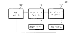
図3は、磁気メモリの磁気接合を製造するための装置100の一例示的な実施形態を示したブロックダイヤグラムである。装置100は追加的な要素が結合されたさらに大きいシステムの一部であり得る。選択的に、装置100は独立形(stand−alone)システムであり得る。明確にするために、装置100の幾つかの要素が図3に図示される。装置100は、互いに連結された反応イオンエッチング(RIE)チャンバー102及びイオンミリングチャンバー104を含む。幾つかの実施形態で、中央インターロックチャンバー(central interlock chamber、図示せず)がRIEチャンバー102及びイオンミリングチャンバー104の間にあり得る。RIEチャンバー102は反応性イオンエッチング(RIE)が遂行されるチャンバーである。そのため、RIEチャンバーは製造工程の間に素子の膜の一部を除去する化学的反応が許諾されるように具備される。また、RIEチャンバー102はRIEチャンバー102内へ反応ガスを導入するガス伝達システム(gas delivery system)を包含することができる。
FIG. 3 is a block diagram illustrating one exemplary embodiment of an
装置100は、磁気接合を定義するのに使用されるイオンミリングチャンバー104を含む。イオンミリングチャンバー104は、イオンガン(ion gun)のようなイオンソース(図示せず)を含み、イオンミリングに相応しいように極めて低い圧力に排気される。
The
また、RIEチャンバー102及びイオンミリングチャンバー104のための真空システム110−1、110−2が図示される。2つの真空システム110−1、110−2が図示され、RIEチャンバー102及びイオンミリングチャンバー104は互いに異なる要件を含む。さらに詳細に、イオンミリングチャンバー104は、イオンソースからイオンが製造される素子に到達することができるように非常に高い真空(例えば、より低い圧力)で進行されることが望ましい。その上、RIEチャンバー102は一般的に反応性イオンエッチングで使用される反応ガスを包含するので、分離された真空システム110−1、110−2を有することが望ましい。イオンミリングチャンバー104が真空システム110−2を包含することによって、前記ガスがイオンミリングチャンバー104の一部から隔離されることが望ましい。しかし、他の実施形態では、単一の真空システムが2つのチャンバー102、104のために使用され得る。
Also shown are vacuum systems 110-1, 110-2 for the
それらの個別の工程段階のための構成に加えて、RIEチャンバー102及びイオンミリングチャンバー104は連結される。より詳細には、RIEチャンバー102及びイオンミリングチャンバー104が連結されることによって、磁気メモリが大気環境(例えば、装置100の外部大気)に露出されずにRIEチャンバー102及びイオンミリングチャンバー104の間を移動することができる。そのため、チャンバー102、104の間で製造される素子を含む基板が移動する間、RIEチャンバー102及びイオンミリングチャンバー104の両方が真空状態であり得る。追加的に、幾つかの移動メカニズム(図示せず)も、装置100の一部であり得る。移動メカニズムは、チャンバーが大気環境から隔離されて(例えば、真空状態)、RIEチャンバー102及びイオンミリングチャンバー104の間を磁気メモリを移動させるのに使用され得る。
In addition to the configuration for these individual process steps, the
図示された実施形態では、RIEチャンバー102及びイオンミリングチャンバー104は直接的に連結されない。そのため、移動チューブ(transfer tube)又は類似要素(analogous component)がチャンバー102、104を連結することができる。他の実施形態では、RIEチャンバー102はイオンミリングチャンバー104と直接的に連結され得る。前記実施形態では、ドア(door)又は類似メカニズム(analogous mechanism)は、使用する間にチャンバー102、104を分離することができる。結果的に、異なる工程がチャンバーのうちの1つのチャンバー102又は104で遂行される間に、他のチャンバー102又は104に影響を及ぼさないことがあり得る。
In the illustrated embodiment, the
前記装置は磁気メモリの磁気接合の製造を改善させるのに使用され得る。例えば、基板上の素子をイオンミリングした後、大気環境に磁気素子が露出されずに反応性イオンエッチングを遂行することができる。類似して、基板上の素子を反応性イオンエッチングした後、大気環境に磁気素子が露出されずにイオンミリングを遂行することができる。このような工程は、磁気接合の性能を改善させ得る。例えば、図2で図示された一般的な方法50で決定される。反応性イオンエッチングを遂行した後、ハードマスク物質の再蒸着(redepostion)があり得る。ハードマスクはタングステンW又はタンタルTaのような物質からなり得る。反応性イオンエッチングには、フッ素F又は塩素Clのようなガスを使用することができる。WF又はWClのような物質の再蒸着が発生し得る。段階54で磁気メモリを大気環境に露出させる時、フッ素F又は塩素Clは空気中の水蒸気と反応してHF又はHClを形成する。このような化合物は非常に酸性であり、磁気物質の下部スタックを損傷させ得る。その結果、自由膜20、バリア膜18、及び/又は被固定膜16が損傷され得る。一般的な磁気接合10の性能は低下され得る。反対に、装置100の使用によって、ハードマスク又は他の磁気接合の反応性イオンエッチング及びイオンミリングが大気環境に露出されずに遂行することができる。結果的に、酸(acid)の形成を防ぐことができる。従って、磁気接合の損傷を防止することができる。その結果、装置100の使用は、装置100を使用して形成された磁気接合の性能を向上させることができる。
The device can be used to improve the manufacture of magnetic junctions in magnetic memories. For example, after ion milling the element on the substrate, reactive ion etching can be performed without exposing the magnetic element to the atmospheric environment. Similarly, after reactive ion etching of the element on the substrate, ion milling can be performed without exposing the magnetic element to the atmospheric environment. Such a process can improve the performance of the magnetic junction. For example, it is determined by the
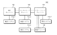
図4は磁気メモリの磁気接合を製造するための装置100’の例示的な実施形態を示したブロックダイヤグラムである。装置100’は追加的な要素が結合されたより大きいシステムの一部であり得る。選択的に、装置100’は独立形システムであり得る。明確にするために、装置100’の幾つかの要素が図4で図示される。装置100’は装置100と類似である。装置100’は、RIEチャンバー102及びイオンミリングチャンバー104と各々類似なRIEチャンバー102’及びイオンミリングチャンバー104’を含む。従って、チャンバー102’、104’の構造及び機能は、チャンバー102、104の構造及び機能と各々類似であり得る。
FIG. 4 is a block diagram illustrating an exemplary embodiment of an apparatus 100 'for manufacturing a magnetic junction of a magnetic memory. Device 100 'may be part of a larger system with additional elements combined. Optionally, device 100 'can be a stand-alone system. For clarity, some elements of device 100 'are illustrated in FIG. Device 100 'is similar to
装置100’はまたインターロックチャンバー106及び蒸着チャンバー108を含む。幾つかの実施形態で、チャンバー106及び/又は108は省略され得る。インターロックチャンバー106はRIEチャンバー102’とイオンミリングチャンバー104’との間を連結する。イオンミリングチャンバー104’は蒸着チャンバー108に連結される。選択的な実施形態で、インターロックチャンバー106はチャンバー102、104、108に直接的に連結される中央チャンバー(central chamber)であり得る。また、インターロックチャンバー106は装置100’のローディング/アンローディング(loading/unloading)のための中央入口(central entrance)であり得る。しかし、他の実施形態で、他のチャンバー102’、104’、及び/又は108の中で1つ以上は直接的な基板のローディング又はアンローディングのための入口を有することができる。図示された実施形態で、各チャンバー102’、104’、106、108は、各々の真空システム110−1’、110−2’、110−3、110−4を各々含む。他の実施形態で、真空システム110−1’、110−2’、110−3、110−4は、多数のチャンバーを真空排気するように(evacuate)結合され得る。
The
インターロックチャンバー106は、例えば真空システム110−3を使用して、大気環境から孤立される。その上、インターロックチャンバー106は、RIEチャンバー102’とイオンミリングチャンバー104’との間を大気環境に露出されずに磁気メモリを移動させるのに利用され得る。例えば、インターロックチャンバー106は真空排気されることができ、磁気メモリはRIEチャンバー102’からインターロックチャンバーへ移動され得る。その後、RIEチャンバー102’はインターロックチャンバー106から孤立されることができる。その後、磁気メモリはインターロックチャンバー106からイオンミリングチャンバー104’へ移動され得る。蒸着チャンバー108はまたイオンミリングチャンバー104’に連結されることによって、磁気メモリがイオンミリングチャンバー104’及び蒸着チャンバー108の間を大気環境に露出ずに移動され得る。その上、磁気メモリがRIEチャンバー102’とイオンミリングチャンバー104’との間を大気環境に露出されずに移動し、磁気メモリがイオンミリングチャンバー104’と蒸着チャンバー108との間を大気環境に露出されずに移動するので、磁気メモリはRIEチャンバー102’と蒸着チャンバー108との間を大気環境に露出されずに移動され得る。
The
装置100’は、装置100の効果を共有する。特に、イオンミリングの後に反応性イオンエッチング及び/又は反応性イオンエッチングの後、イオンミリングは、工程の間で磁気メモリが大気環境に露出されずに遂行することができる。前記記載された理由によって、改善された性能を有する磁気接合が得られる。その上、キャッピング膜のような膜は反応性イオンエッチング及び/又はイオンミリングの後に蒸着されることができるが、工程の間で大気環境に磁気メモリが露出されないこともあり得る。その結果、形成される磁気素子の追加損傷を減少させるか、或いは除去することができる。
The
図5は磁気メモリの磁気接合を製造するための装置100”の例示的な実施形態を示したブロックダイヤグラムである。装置100”は追加的な要素が結合されたさらに大きいシステムの一部であり得る。選択的に装置100”は独立形システムであり得る。明確にするために、装置100”の幾つかの要素を図5で図示する。装置100”は装置100及び装置100’と類似である。装置100”はRIEチャンバー102/102’、イオンミリングチャンバー104/104’、インターロックチャンバー106及び蒸着チャンバー108と各々類似なRIEチャンバー102”、イオンミリングチャンバー104”、インターロックチャンバー106’及び蒸着チャンバー108’を含む。チャンバー102”、104”、106’、108’の構造及び機能はチャンバー102/102’、104/104’、106、108の構造及び機能と各々類似であり得る。
FIG. 5 is a block diagram illustrating an exemplary embodiment of an
インターロックチャンバー106’はすべてのチャンバー102”、104”、108’の中央にある。その結果、磁気メモリは1つのチャンバー102”、104”及び/又は106’から他のチャンバー102”、104”、及び/又は106’へと大気環境に露出されずに移動することができる。したがって、反応性イオンエッチング、イオンミリング、及び蒸着工程のためのチャンバー102”、104”、106’の中でいずれの工程も、工程の間で磁気メモリが大気環境に露出されずに遂行することができる。
The interlock chamber 106 'is in the middle of all the
装置100”は、110−1及び110−2の組み合わせと類似であり、110−1’、110−2’、110−3、及び110−4の組み合わせと類似の単一真空システム110”を含む。それで、真空システム110”はチャンバー102”、104”、106’、及び/又は108’のうちの1つ以上を真空排気する。他の実施形態で、真空システム110”はシステム100又は100’で使用された分離された要素の1つ以上に分けられることができる。
装置100”は、装置100/100’の効果を共有する。特に、イオンミリングの後の反応性イオンエッチング及び/又は反応性イオンエッチングの後のイオンミリングは、工程の間で磁気メモリが大気環境に露出されずに遂行することができる。前記記述された理由によって、磁気接合は改善された性能を有することができる。その上、キャッピング膜のような膜は反応性イオンエッチング及び/又はイオンミリングの後に、工程の間で磁気メモリが大気環境に露出されずに蒸着され得る。従って、形成される磁気素子に対する損傷を減少させるか、或いは除去することができる。
The
図6は前記装置を使用して磁気メモリの磁気接合を製造するための方法150の例示的な実施形態を図示する。簡略化のために、幾つかの段階は、省略され、結合され、挿入されるか、或いは他の順序で遂行することができる。方法150は装置100に関して記述される。しかし、方法150は装置100’、100”、及び/又は他の類似な装置のような他の装置で使用され得る。その上、方法150は磁気メモリの製造に包含され得る。従って、方法150はSTT−RAM又は他の磁気メモリの製造で使用され得る。書込み電流が磁気接合を通じて流れる時、製造される磁気接合は多数の安定された磁気状態の間でスイッチすることができる。
FIG. 6 illustrates an exemplary embodiment of a
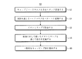
段階152を通じて、磁気接合膜が提供される。段階152は目的とする厚さに目的とする物質を蒸着することを含む。段階152はシード膜、固定膜(例えば、反強磁性体)、被固定膜、非磁性スペーサー膜、及び自由膜の蒸着を含む。他の実施形態で、段階152は単一被固定膜、MgOのようなバリア膜、及び自由膜を提供することを含む。前記実施形態で、段階152はまたMgOのような第2バリア膜、及び第2被固定膜を蒸着することを含む。第1及び第2固定膜がまた蒸着され得る。被固定膜及び/又は自由膜はSAF(合成反強磁性体;synthetic antiferromagnetic)であり得る。
Through
段階154を通じて、ハードマスク膜がまた提供される。例えば、ハードマスク膜はタングステンW及び/又はタンタルTaを包含することができる。段階154は磁気接合膜上にハードマスク膜をブランケット(blanket)蒸着することを含む。例えば、蒸着チャンバーが装置100の一部分であれば、段階152及び154は装置100で遂行することができる。
Through
段階156を通じて、ハードマスクは、反応性イオンエッチングを使用してハードマスク膜から形成される。段階156の反応性イオンエッチングはRIEチャンバー102で遂行することができる。段階156で遂行される反応性イオンエッチングは1mTorr単位の圧力の下で反応ガスを使用することができる。
Through
段階156で反応性イオンエッチングを遂行した後、段階158を通じてイオンミリングを使用して磁気接合を少なくとも部分的に定義する。幾つかの実施形態で、磁気接合は完全に定義される。それで、磁気接合のための段階152で提供されたすべての膜は段階158を通じてミリング(mill)される。他の実施形態で、膜は部分的にミリングされる。磁気接合の定義は他の工程を使用して完成されることができ、追加的なイオンミリング及び/又は追加的な反応性イオンエッチングを包含できるが、これに限定されない。
After performing the reactive ion etch at
段階158のイオンミリングはイオンミリングチャンバー104で遂行することができる。それで、段階158のイオンミリングは、反応性イオンエッチングとイオンミリングとの間で磁気メモリが大気環境に露出されずに遂行することができる。段階156の反応性イオンエッチングで使用されたガスがイオンミリングを妨害することが実質的に防止される。所定の実施形態で、段階156の反応性イオンエッチングで使用されたガスがイオンミリングチャンバー104へ入ることが実質的に防止される。例えば、イオンミリングは10−8乃至10−9Torrの圧力の下で遂行することができる。磁気メモリをRIEチャンバー102へ移動させる前に、RIEチャンバー102はイオンミリングチャンバー104と実質的に同一の圧力に真空排気されることができる。幾つかの実施形態で、磁気メモリがRIEチャンバー102からイオンミリングチャンバー104へ移動される時、チャンバー102、104の両方は真空状態である。選択的にRIEチャンバー102は真空排気されて、非活性ガスが導入されることができる。その後、磁気メモリは望ましくは類似の圧力の下で非活性ガスを含むイオンミリングチャンバー104へ移動され得る。イオンミリングチャンバー104は真空排気され、イオンミリングが進行され得る。他の実施形態で、チャンバー102、104の間で移動は他の方式で遂行することができる。しかし、磁気メモリは、磁気メモリ及び磁気素子が大気環境に露出されずに実質的に段階156及び158での工程で悪影響無くチャンバー102、104の間で移動され得る。
The ion milling of
段階160を通じて、キャッピング膜は選択的に蒸着され得る。キャッピング膜は絶縁物であり得る。例えば、シリコン酸化物、シリコン窒化物及び/又はアルミニウム酸化物が使用され得る。キャッピング膜は磁気接合の側面を損傷から保護するのに使用され得る。幾つかの実施形態で、イオンミリング段階158の後、磁気メモリが大気環境に露出されずにキャッピング膜が蒸着され得る。
Through
方法150は、磁気素子の製造が完成される時まで続くことができる。幾つかの実施形態で、方法150は磁気接合膜の一部を除去して、磁気接合を定義することを完成することを含む。方法150は、構造の追加イオンミリング及び/又は追加反応性イオンエッチングを遂行することを含む。追加的なキャッピング膜がまた蒸着され得る。このような工程の幾つか又は全ては、磁気メモリが大気環境に露出されずに遂行することができる。例えば、磁気メモリは、チャンバー102/102’/102”、104/104’/104”、106/106’及び/又は108/108’の間を装置100/100’/100”を開放することなく移動することができる。
The
方法150は、装置100、100’及び/又は100”の効果を共有することができる。特に、改善された性能と、性能での減少された差異(variation)を有する磁気メモリが製造され得る。したがって、方法150の収率が増加され得る。
The
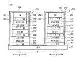
図7は、方法150及び/又は装置100、100’及び/又は100”を使用して製造されたスピン伝達を使用してスイッチ可能な磁気接合210を含む磁気メモリ200の例示的な実施形態を図示する。明確には、図7はスケール通りではない。磁気メモリは基板201を含み、製造された磁気メモリ内の追加的な要素を包含することができる。例えば、トランジスタ(transistor)のような選択素子、導電ライン、及び/又は他の構造が基板に形成され得る。磁気接合210は、シード膜212、被固定膜214、非磁性スペーサー膜216、自由膜218、選択的な第2非磁性スペーサー膜220、選択的な第2被固定膜222、及びキャッピング膜224を含む。図示された実施形態で、被固定膜214は磁気−被固定され(self−pinned)るため、外部固定膜(external pinning layer)を必要としない。しかし、他の実施形態で、AFM膜のような固定膜は、被固定膜214、222の磁気モーメントを固定させるために提供され得る。一般的に、被固定膜214、222の磁気モーメントが面内(plane)にある場合、固定膜が使用され得るが、、被固定膜214、222の磁気モーメントが面と垂直である時は使われない。また、磁気接合210は、磁気接合200を通じて書込み電流が流れる時、自由膜218が安定された磁気状態の間でスイッチされることができるように構成される。それで、自由膜218は、スピン伝達トルクを使用してスイッチすることができる。2つの被固定膜214、222と2つの非磁性スペーサー膜216、220が図示されたが、他の実施形態では単に1つの非磁性スペーサー膜216又は220と1つの被固定膜214又は222が包含され得る。
FIG. 7 illustrates an exemplary embodiment of a
非磁性スペーサー膜216及び/又は220はトンネルリングバリア膜、導電体、又は他の構造であり得る。この時、自由膜218と被固定膜214及び/又は222との間に磁気抵抗が示される。非磁性スペーサー膜216、220は類似な構造を有する必要はない。例えば、2つの膜216、220の全てがトンネルリングバリアであるか、或いは1つはトンネルリングバリアであり、その他の1つは導電体であり得る。他の実施形態で、非磁性スペーサー膜216、220は結晶性MgOトンネルリングバリア膜である。そのような実施形態で、MgOシード膜204は磁気接合200のTMR及び他の特性を改善するために適用され得る。MgOシード膜の存在はトンネルリングバリア膜220の結晶構造を改善させると仮定されている。
The
単一膜として図示されたが、自由膜218及び/又は被固定膜212及び/又は222は多層膜(multiple layers)を包含することができる。例えば、膜214、218、222の1つ以上は、Ruのような薄膜を通じて反強磁性であるか、或いは強磁性として連結された磁気膜を含むSAFであり得る。SAFで、Ru又は他の物質の薄膜が挿入された多層磁気膜が使用され得る。膜214、218、222の1つ以上は、他の多層膜を有することができる。図7には磁化が図示されていないが、自由膜218及び/又は被固定膜230の各々は、面外磁気消去エネルギー(out−of−plane demagnetization energy)を超過する垂直異方性エネルギー(perpendicular anisotropy energy)を有することができる。それで、自由膜210及び/又は被固定膜212、222の各々は面に対して垂直方向の磁気モーメントを有することができる。他の実施形態で、膜214、218及び/又は220の磁気モーメントは各々面内にある。自由膜218、被固定膜214、及び/又は被固定膜222の磁気モーメントの他の方向が可能である。
Although illustrated as a single membrane, the
磁気接合210は、方法150及び/又は装置100、100’及び/又は100”を使用して製造することができるので、方法150及び/又は装置100、100’及び/又は100”の効果を獲得することができる。特に、磁気接合210は性能を向上させ、及び/又は性能での差異を減少させ得る。その上、製造方法150は、磁気接合210の減少された臨界寸法(critical dimension)を許容することができる。例えば、磁気接合210は、20nm以下の直径(又は最も小さい臨界寸法)を有することができる。追加的に、メモリ200は、隣接する磁気接合210の間での200nm以下のさらに小さい間隔(例えば、列又は行のピッチ)を有することができる。幾つかの実施形態で、ピッチは100nmより大きくない。幾つかのそのような実施形態で、ピッチは90nmより大きくない。図示された実施形態で、段階160のキャッピング膜は省略されるか、或いは提供されない。その結果、前記記載された効果に追加的に、さらに密なメモリ(more dense memory)が提供され得る。
The
図8は、方法150及び/又は装置100、100’及び/又は100”を使用して製造されることができるスピン伝達を使用するスイッチ可能な磁気接合210’を含む磁気メモリの例示的な実施形態を図示する。明確には、図8はスケール通りではない。磁気メモリ200’は磁気メモリ200と類似である。磁気メモリ200’は装置100、100’及び100”及び方法150に関して記述される。基板201’及び磁気接合210’は基板201及び磁気接合210と各々類似である。したがって、類似な膜には類似な図面符号を付す。磁気接合210’は、膜212、214、216、218、220、222、224と各々類似な選択的シード膜212’、被固定膜214’、非磁性スペーサー膜216’、自由膜218’、他の非磁性スペーサー膜220’、被固定膜222’、及びキャッピング膜224’を含む。従って、追加的なシード膜212’、被固定膜214’、反磁性スペーサー膜216’、自由膜218’、他の反磁性スペーサー膜220’、被固定膜222’及びキャッピング膜224’の幾何学的な結晶構造、物質及び特性は、膜212、214、216、218、220、222、224と各々類似である。さらに、基板201’は基板201と類似であり得る。2つの被固定膜214’、222’と2つの反磁性スペーサー膜216’、220’が図示されたが、他の実施形態では、単に1つの反磁性スペーサー膜216’又は220’及び1つの被固定膜214’又は222’が包含され得る。
FIG. 8 illustrates an exemplary implementation of a magnetic memory including a switchable
追加的に、磁気接合210’は、キャッピング膜230を包含することができる。キャッピング膜230は、磁気接合210’が完全に定義された後、段階160で蒸着される。その結果、キャッピング膜230は磁気接合210’の側面を実質的に覆う。幾つかの実施形態で、キャッピング膜230はシリコン窒化物、シリコン酸化物、及び/又はアルミニウム酸化物であり得る。しかし、他の絶縁物質が使用され得る。図示された実施形態で、接合210’がミリングされた後、イオンミリング及びキャップ230蒸着の間で、メモリ200’が大気環境に露出されず、キャッピング膜230は、段階160で蒸着され得る。
In addition, the
磁気接合210’は、方法150及び/又は装置100、100’及び/又は100”を使用して製造することができるので、方法150及び/又は装置100、100’及び/又は100”の効果を獲得することができる。特に、磁気接合210’は、性能を向上させ、性能での差異を減少させ得る。その上、製造方法150は磁気接合210’の減少された臨界寸法を許容することができる。例えば、磁気接合210’は、20nm以下の直径(又は最も小さい臨界寸法)を有することができる。メモリ200’は、隣接する磁気接合210’の間での200nm以下のさらに小さい間隔(例えば、列又は行ピッチ)を有することができる。幾つかの実施形態で、ピッチは100nmより大きくない。幾つかのそのような実施形態で、ピッチは90nmより大きくない。従って、前記記載された効果に追加的に、さらに密なメモリが提供され得る。
Since the magnetic junction 210 'can be manufactured using the
図9は、方法150及び/又は装置100、100’及び/又は100”を使用して製造できるスピン伝達を使用するスイッチ可能な磁気接合210”を含む磁気メモリ200”の例示的な実施形態を図示する。明確には、図9はスケール通りではない。磁気メモリ200”は、磁気メモリ200、200’と類似である。磁気メモリ200”は、装置100、100’及び100”及び方法150に関して記述される。基板201”及び磁気接合210”は、基板201/201’及び磁気接合210/210’と各々類似である。したがって、類似な膜には類似な図面符号を付す。磁気接合210”は、膜212/212’、214/214’、216/216’、218/218’、220/220’、222/222’、224/224’、230と各々類似な選択的シード膜212”、被固定膜214”、非磁性スペーサー膜216”、自由膜218”、他の非磁性スペーサー膜220”、被固定膜222”、キャッピング膜224”、及びキャッピング膜230’を含む。従って、追加的なシード膜212”、被固定膜214”、反磁性スペーサー膜216”、自由膜218”、他の反磁性スペーサー膜220”、被固定膜222”、キャッピング膜224”、及びキャッピング膜230’の幾何学的な、結晶構造、物質、及び特性は膜212/212’、214/214’、216/216’、218/218’、220/220’、222/222’、224/224’、230と各々類似である。さらに、基板201”は、基板201/201’と類似であり得る。2つの被固定膜214”、222”と2つの反磁性スペーサー膜216”、220”が図示されたが、他の実施形態では、単に1つの反磁性スペーサー膜216”又は220”及び1つの被固定膜214”又は222”が包含され得る。
FIG. 9 illustrates an exemplary embodiment of a
磁気接合210”は、キャッピング膜230’及び再蒸着膜232を包含することができる。さらに詳細に、磁気接合210”は、段階158を通じて部分的にミリングされ、段階160でキャッピング膜230’が蒸着される。図示された実施形態で、磁気接合210”は段階158で、反磁性スペーサー膜216”及び被固定膜214”の間の界面に至るまでミリングされる。しかし、他の実施形態で、ミリングは他の膜又は他の界面で終了され得る。その後、磁気接合210”の定義が完成される。例えば、追加イオンミリング及び/又は反応性イオンエッチングが遂行することができる。しかし、膜214”、212”の一部を除去する間、再蒸着膜232が形成される。
The
磁気接合210”は、方法150及び/又は装置100、100’及び/又は100”を使用して製造することができるので、方法150及び/又は装置100、100’及び/又は100”の効果を獲得することができる。特に、磁気接合210”は、性能を向上させ、性能での差異を減少させ得る。その上、製造方法150は磁気接合210”の減少された臨界寸法を許容することができる。例えば、磁気接合210”は20nm以下の直径(又は最も小さい臨界寸法)を有することができる。メモリ200”は隣接する磁気接合210”の間での200nm以下のさらに小さい間隔(例えば、列又は行ピッチ)を有することができる。幾つかの実施形態で、ピッチは100nmより大きくない。幾つかのそのような実施形態で、ピッチは90nmより大きくない。それで、前記記載された効果に追加的に、さらに密なメモリが提供され得る。
Since the
図10は、方法150及び/又は装置100、100’及び/又は100”を使用して製造できるスピン伝達を使用するスイッチ可能な磁気接合210’’’を含む磁気メモリ200’’’の例示的な実施形態を図示する。明確には、図10はスケール通りではない。磁気メモリ200’’’は、磁気メモリ200、200’、200”と類似である。磁気メモリ200’’’は、装置100、100’及び100”及び方法150に関して記述される。基板201’’’及び磁気接合210’’’は、基板201/201’/201”及び磁気接合210/210’/210”と各々類似である。したがって、類似な膜には類似な図面符号を付す。磁気接合210’’’は、膜212/212’/212”、214/214’/214”、216/216’/216”、218/218’/218”、220/220’/220”、222/222’/222”、224/224’/224”、230/230’、232と各々類似な選択的シード膜212’’’、被固定膜214’’’、非磁性スペーサー膜216’’’、自由膜218’’’、他の非磁性スペーサー膜220’’’、被固定膜222’’’、キャッピング膜224’’’、キャッピング膜230’’及び再蒸着膜232を含む。従って、追加的なシード膜212’’’、被固定膜214’’’、反磁性スペーサー膜216’’’、自由膜218’’’、他の反磁性スペーサー膜220’’’、被固定膜222’’’、キャッピング膜224’’’、キャッピング膜230”及び再蒸着膜232’の幾何学的な結晶構造、物質及び特性は膜212/212’/212”、214/214’/214”、216/216’/216”、218/218’/218”、220/220’/220”、222/222’/222”、224/224’/224”、230/230’、232と各々類似である。さらに、基板201’’’は基板201/201’/201”と類似であり得る。2つの被固定膜214’’’、222’’’と2つの反磁性スペーサー膜216’’’、220’’’が図示されたが、他の実施形態で、単に1つの反磁性スペーサー膜216’’’又は220’’’及び1つの被固定膜214’’’又は222’’’が包含され得る。
FIG. 10 illustrates an exemplary
磁気接合210’’’は、キャッピング膜230”、再蒸着膜232’、及び追加キャッピング膜234を包含することができる。さらに詳細に、磁気接合210’’’は、段階158を通じて部分的にミリングされ、段階160でキャッピング膜230”が蒸着される。図示された実施形態で、磁気接合210’’’は、段階158で、反磁性スペーサー膜216’’’及び被固定膜214’’’の間の界面に至るまでミリングされる。しかし、他の実施形態で、ミリングは他の膜又は他の界面で終了され得る。その後、磁気接合210’’’の定義が完成される。例えば、追加イオンミリング及び/又は反応性イオンエッチングが遂行することができる。しかし、膜214’’’、212’’’の一部を除去する間、再蒸着膜232’が形成される。その後、追加的なキャッピング膜234が蒸着される。
The
磁気接合210’’’は、方法150及び/又は装置100、100’及び/又は100”を使用して製造することができるので、方法150及び/又は装置100、100’及び/又は100”の効果を獲得することができる。特に、磁気接合210’’’は性能を向上させ、性能での差異を減少させ得る。その上、製造方法150は、磁気接合210’’’の減少された臨界寸法を許容することができる。例えば、磁気接合210’’’は20nm以下の直径(又は最も小さい臨界寸法)を有することができる。メモリ200’’’は隣接する磁気接合210’’’間での200nm以下のさらに小さい間隔(例えば、列又は行ピッチ)を有することができる。幾つかの実施形態で、ピッチは100nmより大きくない。幾つかのそのような実施形態で、ピッチは90nmより大きくない。それで、前記記載された効果に追加的に、さらに密なメモリが提供され得る。
The magnetic junction 210 '' 'can be manufactured using the
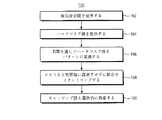
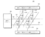
図11は、磁気メモリで磁気接合を製造するための方法170の例示的な実施形態を図示する。簡略化のために、幾つかの段階は省略されるか、結合されるか、挿入されるか、或いは他の順序で遂行することができる。方法170は、装置100”に関して記述される。しかし、方法170は、装置100、110’のような他の装置及び/又は他の類似な装置で使用され得る。さらに、方法150は、磁気メモリの製造に包含され得る。そして、方法150は、STT−RAM又は磁気メモリの製造に使用され得る。図12乃至図16は方法170を使用する製造の間の磁気メモリ250の例示的な実施形態を図示するダイヤグラムである。明確には、図12乃至図16はスケール通りではなく、メモリ250の一部が省略される。方法170及び素子250がまた特別な膜に関して記述される。しかし、幾つかの実施形態で、前記膜は多層のサブ膜(multiple sublayers)を包含することができる。書込み電流が磁気接合を通じて流れる時、製造された磁気接合は多数の安定された磁気状態の間でスイッチ可能である。
FIG. 11 illustrates an exemplary embodiment of a
段階172を通じて、磁気接合膜が提供される。段階172は、目的とする厚さに目的とする物質が蒸着されることを含む。段階172は、シード膜、固定膜(例えば、反強磁性体)、被固定膜、非磁性スペーサー膜、及び自由膜の蒸着を含む。幾つかの実施形態で、段階172は単一被固定膜、MgOのようなバリア膜、及び自由膜を提供することを含む。幾つかの実施形態で、段階172はまたMgOのような第2バリア膜及び第2被固定膜を蒸着することを含む。第1及び第2固定膜がまた蒸着され得る。被固定膜及び/又は自由膜はSAFであり得る。追加的に自由膜及び/又は被固定膜に隣接するCoFeBのような高いスピン分極膜(high spin polarization layers)がまた提供され得る。従って、段階172は段階152と類似である。
Through
段階174を通じてハードマスク膜が提供される。ハードマスクは例えば、タングステンW、タンタルTa、又は他の膜を包含することができる。段階174は磁気接合膜上にハードマスク膜をブランケット(blanket)蒸着することを包含することができる。したがって、段階174は方法150の段階154と類似である。段階172及び段階174は装置100”の例えば蒸着チャンバー108’で遂行することができる。
A hard mask film is provided through
段階176を通じて、反応性イオンエッチングを使用してハードマスク膜からハードマスクを形成する。段階176の反応性イオンエッチングは、RIEチャンバー102”で遂行することができる。段階176で遂行された反応性イオンエッチングは、1mTorrの圧力で反応ガスを使用することができる。図12は段階176を遂行した後の磁気メモリ250を図示する。それで、基板251は選択的シード膜262、被固定膜264、高いスピン分極CoFeB膜266、非磁性スペーサー膜268、自由膜270、第2非磁性スペーサー膜272、第2高いスピン分極CoFeB膜274、被固定膜276、及びキャッピング膜278の下にある。このような膜262、264、268、270、272、及び274は磁気接合210/210’/210”/210’’’の膜212/212’/212’’/212’’’、214/214’/214’’/214’’’、216/216’/216’’/216’’’、218/218’/218’’/218’’’、220/220’/220’’/220’’’、222/222’/222’’/222’’’及び224/224’/224’’/224’’’と各々類似である。また、ハードマスク252が図示される。ハードマスク252は磁気接合260を形成するのに使用される。磁気接合260はメモリで、臨界寸法d及びピッチpを有する。ハードマスク252はRIEチャンバー102”で遂行される反応性イオンエッチングを使用して単一膜から形成される。
Through
段階178を通じて、反応性イオンエッチングを遂行した後、磁気メモリ250はRIEチャンバー102”からイオンミリングチャンバー104”へと移送され、部分的にイオンミリングされる。前記移送は、磁気メモリ250が大気環境に露出されずに達成される。つまり、移送は真空で、非活性ガス存在の下で、又は他の類似な方式で行われ得る。イオンミリングは、磁気メモリ250の表面から傾くように遂行される。一般的にこのような傾斜は20°である。図示された実施形態で、磁気接合は部分的に定義される。それで、磁気接合のために段階172で提供された膜262、264、266、268、270、272、274、276、及び278の一部のみが段階178を通じてミリングされる。段階178のイオンミリングは、反応性イオンエッチング及びイオンミリングの間で大気環境に基板(及び形成された磁気接合260)が露出されずに遂行される。
After performing reactive ion etching through
段階180を通じてキャッピング膜が蒸着される。キャッピング膜は絶縁物であり得る。例えば、シリコン酸化物、シリコン窒化物及び/又はアルミニウム酸化物が使用され得る。イオンミリング段階の後に、イオンミリング段階178の後、大気環境に磁気メモリが露出されずにキャッピング膜が蒸着される。例えば、磁気メモリ250はイオンミリングチャンバー104”から蒸着チャンバー108’へと移送され、蒸着チャンバー108’でキャッピング膜が蒸着される。図13は、段階180を遂行した後の磁気メモリ250を図示する。図示された実施形態で、キャッピング膜278’及び被固定膜276’が定義される。追加的に、キャッピング膜280が蒸着される。
A capping film is deposited through
段階182を通じて大気環境に磁気メモリ250が露出されずに、追加的な反応性イオンエッチングが遂行される。段階182は、磁気メモリ250を蒸着チャンバー108’からRIEチャンバー102”へと移送して遂行することができる。前記移送は真空の下で、非活性ガス存在の下で、又は他の類似な方式で遂行される。図14は、段階182を遂行した磁気メモリ250を図示する。それで、膜268’、270’、272’、274’は磁気接合260のために定義される。追加的に再蒸着膜282が磁気接合260の側面上に形成される。
An additional reactive ion etch is performed without exposing the
その後、段階184を通じて磁気メモリは再びイオンミリングされる。イオンミリングは、磁気メモリ250が大気環境に露出されずに遂行される。段階184は磁気メモリ250をRIEチャンバー102”からイオンミリングチャンバー104”へと移送させて遂行することができる。前記移送は真空の下で、非活性ガスの存在の下で、又は他の類似な方式で遂行することができる。図15は、段階184を遂行した後の磁気メモリ250を図示する。それで、膜266’、264、262’が定義される。それで、磁気接合260が形成される。
Thereafter, the magnetic memory is ion milled again through
段階186を通じてキャッピング膜が蒸着される。キャッピング膜は絶縁物であり得る。例えば、シリコン酸化物、シリコン窒化物、及び/又はアルミニウム酸化物が使用され得る。イオンミリング段階184の後に、磁気メモリが大気環境に露出されずにキャッピング膜が蒸着される。例えば、磁気メモリ250がイオンミリングチャンバー104”で蒸着チャンバー108’へと移動され、蒸着チャンバー108’でキャッピング膜が蒸着される。図16は、段階186を遂行した後の磁気メモリ250を図示する。キャッピング膜284が蒸着される。結果的に、磁気メモリ250が大気環境に露出されても磁気接合260は大気環境に露出されない。磁気メモリ250は、磁気接合260に損傷無く装置100”から取り出される。図示された実施形態で、以後に定義される膜は、キャッピング膜280/280’及び再蒸着膜282/282’の存在によって、さらに大きい臨界寸法を有する。他の実施形態で、再蒸着膜282/282’及び/又はキャッピング膜280/280’の一部又は全部が段階の間で除去され得る。
A capping film is deposited through
段階186によって磁気接合260が完全に定義されなければ、段階182、184、及び186を反複して磁気接合260を完全に定義する。それで、磁気接合260は反応性イオンエッチング、イオンミリング、及びキャッピング膜の蒸着の組み合わせを含むハイブリッド工程(hybrid process)を使用して定義され得る。
If
方法170を使用して、磁気接合260が形成され得る。磁気接合260は、磁気メモリ250が大気環境に露出されずに定義されるので、磁気接合260の損傷が減少され得る。例えば、再蒸着膜282が大気環境に露出されないので、HF、HCl又は類似の化合物の形成が減少されるか、或いは除去され得る。磁気接合260を定義した後、キャッピング膜284は再蒸着膜282’をくるむことができる。その結果、磁気接合260に対する追加的な損傷を防止することができる。従って、磁気接合260の性能が向上され、方法のための収率が改善され得る。その上、さらに小さい臨界寸法及び/又はさらに小さいピッチを有する磁気接合が達成されることができる。例えば、臨界寸法は20nm以下であり得る。幾つかの実施形態で、ピッチは200nm以下であり得る。幾つかのそのような実施形態で、ピッチは100nm以下であり得る。
Using
図17は、格納セルのメモリ要素で磁気接合を使用するメモリの例示的な実施形態を図示する。磁気接合200、200’、200”、200’’’、260は磁気メモリで使用され得る。図17はメモリ300のような例示的な実施形態である。磁気メモリ300はワードライン選択ドライバー(word line select driver、304)のみならず読出し/書込みカラム選択ドライバー(reading/writing column select driver、302、306)を含む。メモリ300の格納領域は、磁気格納セル310、(storage cells)を含む。各磁気メモリセルは少なくとも1つの磁気接合312及び少なくとも1つの選択素子314を含む。幾つかの実施形態で、選択素子314はトランジスタである。磁気接合312は、1つ以上の磁気接合200、200’、200”、200’’’及び/又は260を包含することができる。1つの磁気接合312がセル310毎に図示されたが、他の実施形態で、セル毎に他の数量の磁気接合312が提供され得る。
FIG. 17 illustrates an exemplary embodiment of a memory that uses a magnetic junction in the memory element of the storage cell.
磁気接合312は、方法150及び/又は170を使用して形成され、装置100、100’又は100”を使用して形成され得る。その結果、磁気メモリ300のピッチ及びセルサイズが減少され得る。結局、さらに密な密度磁気メモリ300が形成され得る。その上、磁気接合310の損傷が低減されるので、磁気メモリ300に対する収率が増加する。
The
磁気接合を提供する方法及び装置と磁気接合を含むメモリを記述する。方法及びシステムは図示された例示的な実施形態と共に記述され、当該技術で通常の技術者は実施形態に対する多様な変形を容易に認識し、変形は方法及びシステムのマッピング及び範囲内にある。したがって、当業者は、添付された請求項のマッピング及び範囲から逸脱することなく多様な変形をなすことができる。 A method and apparatus for providing a magnetic junction and a memory including the magnetic junction are described. The methods and systems are described in conjunction with the illustrated exemplary embodiments, and those skilled in the art will readily recognize various modifications to the embodiments, which are within the mapping and scope of the methods and systems. Accordingly, those skilled in the art can make various modifications without departing from the mapping and scope of the appended claims.
102:RIEチャンバー
104:イオンミリングチャンバー
106:インターロックチャンバー
108:蒸着チャンバー
110:真空システム
102: RIE chamber 104: Ion milling chamber 106: Interlock chamber 108: Deposition chamber 110: Vacuum system
Claims (27)
反応性イオンエッチングチャンバーと、
イオンミリングチャンバーと、を含み、
前記反応性イオンエッチングチャンバー及び前記イオンミリングチャンバーが連結されることによって、前記磁気メモリが前記反応性イオンエッチングチャンバー及び前記イオンミリングチャンバーの間を大気環境に露出されずに移動することができる装置。 In an apparatus used to manufacture a magnetic memory comprising a number of magnetic junctions on a substrate,
A reactive ion etching chamber;
An ion milling chamber,
An apparatus that allows the magnetic memory to move between the reactive ion etching chamber and the ion milling chamber without being exposed to an atmospheric environment by connecting the reactive ion etching chamber and the ion milling chamber.
前記インターロックチャンバーは前記大気環境から孤立され、前記磁気メモリを前記反応性イオンエッチングチャンバーと前記イオンミリングチャンバーとの間で前記大気環境に露出されずに移動するように許容する請求項1に記載の装置。 An interlock chamber connected to the reactive ion etching chamber and the ion milling chamber;
The interlock chamber is isolated from the atmospheric environment and allows the magnetic memory to move between the reactive ion etching chamber and the ion milling chamber without being exposed to the atmospheric environment. Equipment.
前記磁気メモリは前記イオンミリングチャンバーと前記蒸着チャンバーとの間を移動することができる請求項2に記載の装置。 A vapor deposition chamber connected to at least the ion milling chamber;
The apparatus of claim 2, wherein the magnetic memory is movable between the ion milling chamber and the deposition chamber.
前記少なくとも1つの磁気接合のための多数の磁気接合膜を提供することと、
前記多数の磁気接合膜上にハードマスク膜を提供することと、
反応性イオンエッチングを使用して前記ハードマスク膜からハードマスクを形成することと、
前記反応性イオンエッチングを遂行した後、前記磁気メモリを大気環境へ露出させずに前記多数の磁気接合膜をイオンミリングすることと、を含み、
前記多数の磁気接合膜をイオンミリングすることは前記少なくとも1つの磁気接合の各々の少なくとも一部を定義する方法。 A method for providing at least one magnetic junction on a substrate for use in a magnetic memory, the magnetic junction switching between a number of stable magnetic states when a write current flows through the magnetic junction. Arranged so that it can
Providing a plurality of magnetic bonding films for the at least one magnetic bonding;
Providing a hard mask film on the plurality of magnetic bonding films;
Forming a hard mask from the hard mask film using reactive ion etching;
After performing the reactive ion etching, ion-milling the multiple magnetic bonding films without exposing the magnetic memory to an atmospheric environment,
Ion milling the plurality of magnetic junction films defines at least a portion of each of the at least one magnetic junction.
前記多数の磁気接合膜をイオンミリングする段階の後、前記磁気メモリが大気環境に露出されない請求項5に記載の方法。 Further comprising providing a capping film on the at least one magnetic junction after ion milling of the plurality of magnetic junction films;
The method of claim 5, wherein the magnetic memory is not exposed to an atmospheric environment after ion milling the plurality of magnetic bonding films.
前記キャッピング膜を提供する段階の後に、前記磁気メモリを前記大気環境に露出させずに少なくとも1回の追加反応性イオンエッチングを遂行することをさらに含む請求項6に記載の方法。 The ion milling step defines only a portion of each of the at least one magnetic junction;
The method of claim 6, further comprising performing at least one additional reactive ion etch after the step of providing the capping film without exposing the magnetic memory to the atmospheric environment.
前記イオンミリング段階は第2基準膜を限定し、
前記少なくとも1回の追加反応性イオンエッチングは前記第2バリア膜、前記自由膜及び前記第1バリア膜の少なくとも一部を限定する請求項8に記載の方法。 The plurality of magnetic bonding films include a first reference film, a first barrier film, a free film, a second barrier film, and a second free film,
The ion milling step defines a second reference membrane;
9. The method of claim 8, wherein the at least one additional reactive ion etch defines at least a portion of the second barrier film, the free film, and the first barrier film.
前記少なくとも1回の追加イオンミリングは、前記少なくとも1回の追加反応性イオンエッチングを遂行した後、前記磁気メモリが大気環境に露出されずに少なくとも1つの磁気接合の追加的な一部を限定することを含む請求項8に記載の方法。 Further comprising performing at least one additional ion milling after performing the at least one additional reactive ion etching;
The at least one additional ion milling defines an additional portion of the at least one magnetic junction after the at least one additional reactive ion etch is performed and the magnetic memory is not exposed to an atmospheric environment. 9. The method of claim 8, comprising:
前記少なくとも1回の追加イオンミリングを提供する段階の後、前記磁気メモリは大気環境に露出されない方法。 Providing at least one capping membrane after the at least one additional ion milling step;
The method wherein the magnetic memory is not exposed to an atmospheric environment after providing the at least one additional ion milling.
非磁性スペーサー膜と、
自由膜と、を含み、
前記非磁性スペーサー膜は前記被固定膜及び前記自由膜の間に配置され、前記自由膜は20nm以下の幅を有し、
書込み電流が前記磁気接合を通じて流れる時、前記自由膜は多数の安定な磁性状態の間でスイッチ可能であるように前記磁気接合が構成される、磁気メモリで使用される磁気接合。 A fixed membrane;
A non-magnetic spacer film;
A free membrane, and
The nonmagnetic spacer film is disposed between the fixed film and the free film, and the free film has a width of 20 nm or less,
A magnetic junction used in a magnetic memory, wherein the magnetic junction is configured such that the free film is switchable between a number of stable magnetic states when a write current flows through the magnetic junction.
前記非磁性スペーサー膜及び前記自由膜に対応する前記多数の側面の少なくとも一部を覆う第1キャッピング膜をさらに含む請求項12に記載の磁気接合。 The magnetic junction includes multiple sides;
The magnetic junction according to claim 12, further comprising a first capping film covering at least a part of the plurality of side surfaces corresponding to the nonmagnetic spacer film and the free film.
追加被固定膜と、をさらに含み、
前記追加非磁性スペーサー膜は前記自由膜及び前記追加被固定膜の間に配置される請求項13に記載の磁気接合。 An additional non-magnetic spacer film;
An additional immobilization membrane,
The magnetic junction according to claim 13, wherein the additional nonmagnetic spacer film is disposed between the free film and the additional fixed film.
前記第1キャッピング膜及び前記CoFeB膜に対応する前記磁気接合の多数の側面の追加領域を覆う再蒸着膜と、をさらに含む請求項17に記載の磁気接合。 A CoFeB film between the additional nonmagnetic spacer film and the fixed film;
The magnetic junction according to claim 17, further comprising: a redeposition film that covers additional regions on a plurality of side surfaces of the magnetic junction corresponding to the first capping film and the CoFeB film.
多数のビットラインと、を含み、
前記多数の磁気格納セルの各々は幅を有する少なくとも1つの磁気接合を含み、前記少なくとも1つの磁気接合は被固定膜、非磁性スペーサー膜、及び自由膜を含み、前記非磁性スペーサー膜は前記被固定膜及び前記自由膜の間に配置され、
書込み電流が前記磁気接合を通じて流れる時、前記自由膜が多数の安定された磁性状態の間でスイッチ可能であるように前記磁気接合は構成され、前記幅は20nm以下である磁気メモリ。 A number of magnetic storage cells;
A number of bit lines, and
Each of the plurality of magnetic storage cells includes at least one magnetic junction having a width, and the at least one magnetic junction includes a fixed film, a nonmagnetic spacer film, and a free film, and the nonmagnetic spacer film includes the covered film. Arranged between the fixed membrane and the free membrane,
A magnetic memory wherein the magnetic junction is configured such that the free film can switch between a number of stable magnetic states when the write current flows through the magnetic junction and the width is 20 nm or less.
前記少なくとも1つの磁気接合の各々は、前記非磁性スペーサー膜及び前記自由膜に対応する多数の側面の少なくとも一部を覆う第1キャッピング膜をさらに含む請求項19に記載の磁気メモリ。 Each of the at least one magnetic junction includes multiple sides;
The magnetic memory according to claim 19, wherein each of the at least one magnetic junction further includes a first capping film covering at least a part of a plurality of side surfaces corresponding to the nonmagnetic spacer film and the free film.
前記追加非磁性スペーサー膜は前記自由膜及び前記追加被固定膜の間に配置される請求項24に記載の磁気メモリ。 Each of the at least one magnetic junction further includes an additional nonmagnetic spacer film and an additional fixed film;
25. The magnetic memory according to claim 24, wherein the additional nonmagnetic spacer film is disposed between the free film and the additional fixed film.
前記追加非磁性スペーサー膜及び前記被固定膜の間のCoFeB膜と、
前記第1キャッピング膜と前記CoFeB膜に対応する前記磁気接合の多数の側面の追加領域とを覆う再蒸着膜と、をさらに含む請求項26に記載の磁気メモリ。 Each of the at least one magnetic junction includes
A CoFeB film between the additional nonmagnetic spacer film and the fixed film;
27. The magnetic memory according to claim 26, further comprising a redeposited film covering the first capping film and additional regions on a plurality of side surfaces of the magnetic junction corresponding to the CoFeB film.
Applications Claiming Priority (2)
| Application Number | Priority Date | Filing Date | Title |
|---|---|---|---|
| US13/553,965 | 2012-07-20 | ||
| US13/553,965 US9129690B2 (en) | 2012-07-20 | 2012-07-20 | Method and system for providing magnetic junctions having improved characteristics |
Related Child Applications (1)
| Application Number | Title | Priority Date | Filing Date |
|---|---|---|---|
| JP2019010149A Division JP2019071480A (en) | 2012-07-20 | 2019-01-24 | Device for manufacturing magnetic memory and method for providing magnetic junction |
Publications (2)
| Publication Number | Publication Date |
|---|---|
| JP2014022751A true JP2014022751A (en) | 2014-02-03 |
| JP2014022751A5 JP2014022751A5 (en) | 2016-09-01 |
Family
ID=49946433
Family Applications (2)
| Application Number | Title | Priority Date | Filing Date |
|---|---|---|---|
| JP2013150526A Pending JP2014022751A (en) | 2012-07-20 | 2013-07-19 | Magnetic junction, magnetic memory, method and system for providing magnetic junction having improved characteristics |
| JP2019010149A Pending JP2019071480A (en) | 2012-07-20 | 2019-01-24 | Device for manufacturing magnetic memory and method for providing magnetic junction |
Family Applications After (1)
| Application Number | Title | Priority Date | Filing Date |
|---|---|---|---|
| JP2019010149A Pending JP2019071480A (en) | 2012-07-20 | 2019-01-24 | Device for manufacturing magnetic memory and method for providing magnetic junction |
Country Status (4)
| Country | Link |
|---|---|
| US (1) | US9129690B2 (en) |
| JP (2) | JP2014022751A (en) |
| KR (1) | KR102056886B1 (en) |
| CN (1) | CN103579497B (en) |
Cited By (12)
| Publication number | Priority date | Publication date | Assignee | Title |
|---|---|---|---|---|
| KR20150112896A (en) * | 2014-03-27 | 2015-10-07 | 램 리써치 코포레이션 | Method to etch non-volatile metal materials |
| JP2017527097A (en) * | 2014-07-25 | 2017-09-14 | スピン トランスファー テクノロジーズ インク | Method for manufacturing MTJ memory device |
| US10468588B2 (en) | 2018-01-05 | 2019-11-05 | Spin Memory, Inc. | Perpendicular magnetic tunnel junction device with skyrmionic enhancement layers for the precessional spin current magnetic layer |
| US10553787B2 (en) | 2015-06-16 | 2020-02-04 | Spin Memory, Inc. | Precessional spin current structure for MRAM |
| US10580827B1 (en) | 2018-11-16 | 2020-03-03 | Spin Memory, Inc. | Adjustable stabilizer/polarizer method for MRAM with enhanced stability and efficient switching |
| US10615335B2 (en) | 2015-04-21 | 2020-04-07 | Spin Memory, Inc. | Spin transfer torque structure for MRAM devices having a spin current injection capping layer |
| US10643680B2 (en) | 2016-01-28 | 2020-05-05 | Spin Memory, Inc. | Memory cell having magnetic tunnel junction and thermal stability enhancement layer |
| US10665777B2 (en) | 2017-02-28 | 2020-05-26 | Spin Memory, Inc. | Precessional spin current structure with non-magnetic insertion layer for MRAM |
| US10672976B2 (en) | 2017-02-28 | 2020-06-02 | Spin Memory, Inc. | Precessional spin current structure with high in-plane magnetization for MRAM |
| US10734574B2 (en) | 2015-04-21 | 2020-08-04 | Spin Memory, Inc. | Method of manufacturing high annealing temperature perpendicular magnetic anisotropy structure for magnetic random access memory |
| US10777736B2 (en) | 2015-07-30 | 2020-09-15 | Spin Memory, Inc. | Polishing stop layer(s) for processing arrays of semiconductor elements |
| US11217745B2 (en) | 2018-09-06 | 2022-01-04 | Toshiba Memory Corporation | Magnetoresistive memory device and method for manufacturing magnetoresistive memory device |
Families Citing this family (12)
| Publication number | Priority date | Publication date | Assignee | Title |
|---|---|---|---|---|
| KR20130017267A (en) * | 2011-08-10 | 2013-02-20 | 에스케이하이닉스 주식회사 | Semiconductor and method for fabricating the same |
| US8901687B2 (en) | 2012-11-27 | 2014-12-02 | Industrial Technology Research Institute | Magnetic device with a substrate, a sensing block and a repair layer |
| KR102078849B1 (en) * | 2013-03-11 | 2020-02-18 | 삼성전자 주식회사 | Magnetoresistive structure, Magnetic Random Access Memory device and Manufacturing Method of the same |
| US9305579B2 (en) * | 2014-01-15 | 2016-04-05 | HGST Netherlands B.V. | Fabrication of side-by-side sensors for MIMO recording |
| US20150263272A1 (en) * | 2014-03-13 | 2015-09-17 | Kazuhiro Tomioka | Manufacturing method of magnetic memory device and manufacturing apparatus of magnetic memory device |
| US9559296B2 (en) | 2014-07-03 | 2017-01-31 | Samsung Electronics Co., Ltd. | Method for providing a perpendicular magnetic anisotropy magnetic junction usable in spin transfer torque magnetic devices using a sacrificial insertion layer |
| US9412786B1 (en) | 2014-10-02 | 2016-08-09 | Everspin Technologies, Inc. | Magnetoresistive device design and process integration with surrounding circuitry |
| KR102276541B1 (en) | 2014-11-27 | 2021-07-13 | 삼성전자주식회사 | Magnetic memory devices and method of manufacturing the same |
| US10177197B2 (en) * | 2015-11-16 | 2019-01-08 | Samsung Electronics Co., Ltd. | Magnetic junctions having elongated free layers |
| KR102368033B1 (en) | 2017-09-20 | 2022-02-25 | 삼성전자주식회사 | Method of manufacturing a magnetoresistive random access device |
| US10446743B2 (en) | 2018-01-11 | 2019-10-15 | Qualcomm Incorporated | Double-patterned magneto-resistive random access memory (MRAM) for reducing magnetic tunnel junction (MTJ) pitch for increased MRAM bit cell density |
| WO2022087943A1 (en) * | 2020-10-29 | 2022-05-05 | Yangtze Memory Technologies Co., Ltd. | Concentric staircase structure in three-dimensional memory device and method thereof |
Citations (6)
| Publication number | Priority date | Publication date | Assignee | Title |
|---|---|---|---|---|
| JP2005101441A (en) * | 2003-09-26 | 2005-04-14 | Anelva Corp | Magnetic resistance multilayer film |
| WO2007032379A1 (en) * | 2005-09-13 | 2007-03-22 | Canon Anelva Corporation | Method and apparatus for manufacturing magnetoresistive device |
| JP2008218829A (en) * | 2007-03-06 | 2008-09-18 | Toshiba Corp | Magnetoresistance element and manufacturing method thereof |
| JP2008235356A (en) * | 2007-03-16 | 2008-10-02 | Toshiba Corp | Semiconductor memory and its manufacturing method |
| JP2012007194A (en) * | 2010-06-22 | 2012-01-12 | Fujifilm Corp | Film formation apparatus and method for manufacturing photoelectric conversion element |
| JP2012204408A (en) * | 2011-03-23 | 2012-10-22 | Toshiba Corp | Manufacturing method of semiconductor device |
Family Cites Families (28)
| Publication number | Priority date | Publication date | Assignee | Title |
|---|---|---|---|---|
| US6984529B2 (en) | 2003-09-10 | 2006-01-10 | Infineon Technologies Ag | Fabrication process for a magnetic tunnel junction device |
| JP2005194589A (en) * | 2004-01-08 | 2005-07-21 | Sony Corp | Vacuum system, and control method therefor |
| KR100561859B1 (en) * | 2004-01-16 | 2006-03-16 | 삼성전자주식회사 | A method forming a nano-sized MTJ cell without contact hole |
| JP2005268252A (en) | 2004-03-16 | 2005-09-29 | Sony Corp | Method of manufacturing magnetic memory device |
| US20060158790A1 (en) * | 2005-01-14 | 2006-07-20 | Hitachi Global Storage Technologies | Magnetoresistive sensor having a novel junction structure for improved track width definition and pinned layer stability |
| US20060168794A1 (en) * | 2005-01-28 | 2006-08-03 | Hitachi Global Storage Technologies | Method to control mask profile for read sensor definition |
| US7639456B2 (en) | 2005-10-06 | 2009-12-29 | Hitachi Global Storage Technologies Netherlands B.V. | Double mill process for patterning current perpendicular to plane (CPP) magnetoresistive devices to minimize barrier shorting and barrier damage |
| US7509729B2 (en) * | 2006-04-25 | 2009-03-31 | Hitachi Global Storage Technologies Netherlands B.V. | Method for making a perpendicular magnetic recording write head |
| JP4630856B2 (en) * | 2006-09-29 | 2011-02-09 | 株式会社東芝 | Method for manufacturing magnetoresistive element |
| US8472149B2 (en) | 2007-10-01 | 2013-06-25 | Tdk Corporation | CPP type magneto-resistive effect device and magnetic disk system |
| JP4473343B2 (en) * | 2007-11-09 | 2010-06-02 | キヤノンアネルバ株式会社 | Inline wafer transfer device |
| JP4494523B2 (en) * | 2007-11-09 | 2010-06-30 | キヤノンアネルバ株式会社 | Inline type wafer transfer apparatus and substrate transfer method |
| KR100939111B1 (en) | 2007-12-21 | 2010-01-28 | 주식회사 하이닉스반도체 | Method for forming magnetic tunnel junction device |
| JP2009176806A (en) | 2008-01-22 | 2009-08-06 | Fujitsu Ltd | Nonvolatile magnetic memory element |
| JP4875037B2 (en) * | 2008-09-24 | 2012-02-15 | 株式会社東芝 | Magnetic memory, reproducing method thereof, and writing method |
| US7829923B2 (en) | 2008-10-23 | 2010-11-09 | Qualcomm Incorporated | Magnetic tunnel junction and method of fabrication |
| US7989224B2 (en) | 2009-04-30 | 2011-08-02 | International Business Machines Corporation | Sidewall coating for non-uniform spin momentum-transfer magnetic tunnel junction current flow |
| US8159866B2 (en) * | 2009-10-30 | 2012-04-17 | Grandis, Inc. | Method and system for providing dual magnetic tunneling junctions usable in spin transfer torque magnetic memories |
| US8422285B2 (en) * | 2009-10-30 | 2013-04-16 | Grandis, Inc. | Method and system for providing dual magnetic tunneling junctions usable in spin transfer torque magnetic memories |
| US8254162B2 (en) * | 2010-01-11 | 2012-08-28 | Grandis, Inc. | Method and system for providing magnetic tunneling junctions usable in spin transfer torque magnetic memories |
| JP2011198416A (en) * | 2010-03-19 | 2011-10-06 | Toshiba Corp | Magnetic memory |
| US8981502B2 (en) | 2010-03-29 | 2015-03-17 | Qualcomm Incorporated | Fabricating a magnetic tunnel junction storage element |
| JP2012014779A (en) * | 2010-06-30 | 2012-01-19 | Ulvac Japan Ltd | Method for manufacturing magnetic recording medium |
| US8374048B2 (en) * | 2010-08-11 | 2013-02-12 | Grandis, Inc. | Method and system for providing magnetic tunneling junction elements having a biaxial anisotropy |
| US8399941B2 (en) * | 2010-11-05 | 2013-03-19 | Grandis, Inc. | Magnetic junction elements having an easy cone anisotropy and a magnetic memory using such magnetic junction elements |
| JP6043478B2 (en) * | 2010-12-07 | 2016-12-14 | 三星電子株式会社Samsung Electronics Co.,Ltd. | Storage node including free magnetic layer of magnetic anisotropic material, magnetic memory device including the same, and manufacturing method thereof |
| US8432009B2 (en) * | 2010-12-31 | 2013-04-30 | Grandis, Inc. | Method and system for providing magnetic layers having insertion layers for use in spin transfer torque memories |
| US8446761B2 (en) * | 2010-12-31 | 2013-05-21 | Grandis, Inc. | Method and system for providing multiple logic cells in a single stack |
-
2012
- 2012-07-20 US US13/553,965 patent/US9129690B2/en active Active
-
2013
- 2013-07-18 KR KR1020130084835A patent/KR102056886B1/en active IP Right Grant
- 2013-07-19 JP JP2013150526A patent/JP2014022751A/en active Pending
- 2013-07-22 CN CN201310308993.4A patent/CN103579497B/en active Active
-
2019
- 2019-01-24 JP JP2019010149A patent/JP2019071480A/en active Pending
Patent Citations (6)
| Publication number | Priority date | Publication date | Assignee | Title |
|---|---|---|---|---|
| JP2005101441A (en) * | 2003-09-26 | 2005-04-14 | Anelva Corp | Magnetic resistance multilayer film |
| WO2007032379A1 (en) * | 2005-09-13 | 2007-03-22 | Canon Anelva Corporation | Method and apparatus for manufacturing magnetoresistive device |
| JP2008218829A (en) * | 2007-03-06 | 2008-09-18 | Toshiba Corp | Magnetoresistance element and manufacturing method thereof |
| JP2008235356A (en) * | 2007-03-16 | 2008-10-02 | Toshiba Corp | Semiconductor memory and its manufacturing method |
| JP2012007194A (en) * | 2010-06-22 | 2012-01-12 | Fujifilm Corp | Film formation apparatus and method for manufacturing photoelectric conversion element |
| JP2012204408A (en) * | 2011-03-23 | 2012-10-22 | Toshiba Corp | Manufacturing method of semiconductor device |
Cited By (16)
| Publication number | Priority date | Publication date | Assignee | Title |
|---|---|---|---|---|
| JP2015192150A (en) * | 2014-03-27 | 2015-11-02 | ラム リサーチ コーポレーションLam Research Corporation | Method of etching non-volatile metal materials |
| KR102318520B1 (en) * | 2014-03-27 | 2021-10-28 | 램 리써치 코포레이션 | Method to etch non-volatile metal materials |
| KR20150112896A (en) * | 2014-03-27 | 2015-10-07 | 램 리써치 코포레이션 | Method to etch non-volatile metal materials |
| JP2017527097A (en) * | 2014-07-25 | 2017-09-14 | スピン トランスファー テクノロジーズ インク | Method for manufacturing MTJ memory device |
| US10615335B2 (en) | 2015-04-21 | 2020-04-07 | Spin Memory, Inc. | Spin transfer torque structure for MRAM devices having a spin current injection capping layer |
| US10734574B2 (en) | 2015-04-21 | 2020-08-04 | Spin Memory, Inc. | Method of manufacturing high annealing temperature perpendicular magnetic anisotropy structure for magnetic random access memory |
| US10553787B2 (en) | 2015-06-16 | 2020-02-04 | Spin Memory, Inc. | Precessional spin current structure for MRAM |
| US10777736B2 (en) | 2015-07-30 | 2020-09-15 | Spin Memory, Inc. | Polishing stop layer(s) for processing arrays of semiconductor elements |
| US10643680B2 (en) | 2016-01-28 | 2020-05-05 | Spin Memory, Inc. | Memory cell having magnetic tunnel junction and thermal stability enhancement layer |
| US10665777B2 (en) | 2017-02-28 | 2020-05-26 | Spin Memory, Inc. | Precessional spin current structure with non-magnetic insertion layer for MRAM |
| US10672976B2 (en) | 2017-02-28 | 2020-06-02 | Spin Memory, Inc. | Precessional spin current structure with high in-plane magnetization for MRAM |
| US11271149B2 (en) | 2017-02-28 | 2022-03-08 | Integrated Silicon Solution, (Cayman) Inc. | Precessional spin current structure with nonmagnetic insertion layer for MRAM |
| US11355699B2 (en) | 2017-02-28 | 2022-06-07 | Integrated Silicon Solution, (Cayman) Inc. | Precessional spin current structure for MRAM |
| US10468588B2 (en) | 2018-01-05 | 2019-11-05 | Spin Memory, Inc. | Perpendicular magnetic tunnel junction device with skyrmionic enhancement layers for the precessional spin current magnetic layer |
| US11217745B2 (en) | 2018-09-06 | 2022-01-04 | Toshiba Memory Corporation | Magnetoresistive memory device and method for manufacturing magnetoresistive memory device |
| US10580827B1 (en) | 2018-11-16 | 2020-03-03 | Spin Memory, Inc. | Adjustable stabilizer/polarizer method for MRAM with enhanced stability and efficient switching |
Also Published As
| Publication number | Publication date |
|---|---|
| KR102056886B1 (en) | 2019-12-18 |
| US9129690B2 (en) | 2015-09-08 |
| CN103579497B (en) | 2017-04-12 |
| US20140022839A1 (en) | 2014-01-23 |
| JP2019071480A (en) | 2019-05-09 |
| CN103579497A (en) | 2014-02-12 |
| KR20140012595A (en) | 2014-02-03 |
Similar Documents
| Publication | Publication Date | Title |
|---|---|---|
| JP2019071480A (en) | Device for manufacturing magnetic memory and method for providing magnetic junction | |
| US9455400B2 (en) | Magnetic tunnel junction for MRAM applications | |
| US9269893B2 (en) | Replacement conductive hard mask for multi-step magnetic tunnel junction (MTJ) etch | |
| US8722543B2 (en) | Composite hard mask with upper sacrificial dielectric layer for the patterning and etching of nanometer size MRAM devices | |
| US8133745B2 (en) | Method of magnetic tunneling layer processes for spin-transfer torque MRAM | |
| US11217744B2 (en) | Magnetic memory device with multiple sidewall spacers covering sidewall of MTJ element and method for manufacturing the same | |
| US9755141B2 (en) | Method for fabricating MRAM bits on a tight pitch | |
| JP2015179844A (en) | Method for providing perpendicular magnetic anisotropy magnetic junction usable in spin transfer torque magnetic device using sacrificial insertion layer | |
| US9236561B2 (en) | Method and system for providing multiple self-aligned logic cells in a single stack | |
| KR102589614B1 (en) | Magnetic memory device fabrication method using Ru and diamond-like carbon hard masks | |
| US11723217B2 (en) | Magnetic tunnel junction element with RU hard mask for use in magnetic random-access memory | |
| US10868236B2 (en) | Method for manufacturing reduced pitch magnetic random access memory pillar | |
| US10170518B2 (en) | Self-assembled pattern process for fabricating magnetic junctions usable in spin transfer torque applications | |
| US11329217B2 (en) | Method for manufacturing a magnetic random-access memory device using post pillar formation annealing | |
| US9666794B2 (en) | Multi-stage element removal using absorption layers | |
| US20120068280A1 (en) | Magnetic Nano-Ring Device and Method of Fabrication |
Legal Events
| Date | Code | Title | Description |
|---|---|---|---|
| RD04 | Notification of resignation of power of attorney |
Free format text: JAPANESE INTERMEDIATE CODE: A7424 Effective date: 20141226 |
|
| A521 | Request for written amendment filed |
Free format text: JAPANESE INTERMEDIATE CODE: A523 Effective date: 20160715 |
|
| A621 | Written request for application examination |
Free format text: JAPANESE INTERMEDIATE CODE: A621 Effective date: 20160715 |
|
| A977 | Report on retrieval |
Free format text: JAPANESE INTERMEDIATE CODE: A971007 Effective date: 20170406 |
|
| A131 | Notification of reasons for refusal |
Free format text: JAPANESE INTERMEDIATE CODE: A131 Effective date: 20170417 |
|
| A521 | Request for written amendment filed |
Free format text: JAPANESE INTERMEDIATE CODE: A523 Effective date: 20170704 |
|
| A02 | Decision of refusal |
Free format text: JAPANESE INTERMEDIATE CODE: A02 Effective date: 20171127 |
|
| A521 | Request for written amendment filed |
Free format text: JAPANESE INTERMEDIATE CODE: A523 Effective date: 20180323 |
|
| A911 | Transfer to examiner for re-examination before appeal (zenchi) |
Free format text: JAPANESE INTERMEDIATE CODE: A911 Effective date: 20180409 |
|
| A912 | Re-examination (zenchi) completed and case transferred to appeal board |
Free format text: JAPANESE INTERMEDIATE CODE: A912 Effective date: 20180502 |
|
| A521 | Request for written amendment filed |
Free format text: JAPANESE INTERMEDIATE CODE: A523 Effective date: 20190124 |