JP2014018075A - Over-current detection device - Google Patents
Over-current detection device Download PDFInfo
- Publication number
- JP2014018075A JP2014018075A JP2013226385A JP2013226385A JP2014018075A JP 2014018075 A JP2014018075 A JP 2014018075A JP 2013226385 A JP2013226385 A JP 2013226385A JP 2013226385 A JP2013226385 A JP 2013226385A JP 2014018075 A JP2014018075 A JP 2014018075A
- Authority
- JP
- Japan
- Prior art keywords
- overcurrent
- detection device
- current
- current value
- overcurrent detection
- Prior art date
- Legal status (The legal status is an assumption and is not a legal conclusion. Google has not performed a legal analysis and makes no representation as to the accuracy of the status listed.)
- Granted
Links
Images


Abstract
Description
本発明は、電動駆動制御装置の短絡異常による過電流を検出する装置および方法に関する。 The present invention relates to an apparatus and a method for detecting an overcurrent due to a short circuit abnormality in an electric drive control apparatus.
ハイブリッド電気自動車や電気自動車などの電動駆動制御装置においては、直流電圧を交流電圧に変換する電力変換器である電圧形インバータ(以降、本発明ではインバータと称する)が交流モータの可変速駆動用途に使われている。この種のインバータにおいては過電流などの異常検出回路を備えている。 In an electric drive control device such as a hybrid electric vehicle or an electric vehicle, a voltage-type inverter (hereinafter referred to as an inverter in the present invention) that is a power converter that converts a DC voltage into an AC voltage is used for variable-speed driving of an AC motor. It is used. This type of inverter includes an abnormality detection circuit such as overcurrent.
例えば、電動駆動制御装置のインバータの出力側において、導電性異物に起因した出力地絡、接続されたモータ内部での絶縁破壊による線間、もしくは、相間の短絡が起こると、インバータの出力電流振幅が短時間に大きくなり、インバータを構成するトランジスタの最大定格電流や短時間定格電流を超えてしまう過電流状態になる。 For example, if an output ground fault due to conductive foreign matter, a short circuit between lines due to dielectric breakdown inside the connected motor, or a short circuit between phases occurs on the output side of the inverter of the electric drive control device, the output current amplitude of the inverter Becomes larger in a short time, resulting in an overcurrent state that exceeds the maximum rated current and short-time rated current of the transistors constituting the inverter.
特許文献1に開示されているインバータでは、予め設定した閾値を越えると過電流が発生したと判定する。
In the inverter disclosed in
インバータおよびこの周辺回路における次の(1)〜(3)のような故障モードでは、インバータ出力での過電流は数kHzから100kHzを超えるような周波数をもつLCR共振によって発生し、インバータの出力電流は、指令電流に対応した電流(低周波電流)に、共振による振動電流が重畳したような出力電流となることがある。
(1)出力地絡/天絡
(2)出力線間短絡
(3)出力相間短絡
In the failure modes such as the following (1) to (3) in the inverter and the peripheral circuit, overcurrent at the inverter output is generated by LCR resonance having a frequency exceeding several kHz to over 100 kHz, and the output current of the inverter May become an output current in which a vibration current due to resonance is superimposed on a current (low frequency current) corresponding to the command current.
(1) Output ground fault / power fault (2) Output line short circuit (3) Output phase short circuit
特許文献1に開示されている処理を、マイクロコンピュータ(マイコン)を用いて10kHz程度のサンプリング周期で電流値をサンプリングして行う場合、上記(1)〜(3)のような高い周波数の振動電流を正しく検知できない。
また、特許文献1に開示されているようなコンパレータを用い、電流振幅が予め設定した閾値を越えると過電流が発生したと判定する方法を採用した場合においても、正しく過電流を検知することが困難な場合がある。
When the processing disclosed in
Even when a comparator such as that disclosed in
(1)請求項1に記載の過電流検出装置は、モータを駆動するために直流電流を3相交流に変換するインバータと、インバータに流れる直流電圧値を検出する直流電圧検出器と、3相交流の各々の相電流値を検出する相電流検出器と、モータの回転角を検出する回転位置検出器と、相電流検出器からの相電流値、回転位置検出器からのモータ回転角検出値、および上位制御装置からの速度指令もしくはトルク指令に基づいて、インバータの出力電流を制御するゲート駆動回路を所定のサイクル毎に制御する制御回路と、所定のサイクル毎に相電流検出器で検出した相電流値から過電流を検出する第1の判定回路とを備え、第1の判定回路は、相電流値が所定の振幅閾値を越えるか否かを、所定の振幅閾値を越える相電流値の周波数検出を行うことによって判定し、周波数が検出された場合は過電流と判定することを特徴とする過電流検出装置である。
(2)請求項2に記載の発明は、請求項1に記載の過電流検出装置において、所定のサイクル毎に過電流を検出する第2の判定回路をさらに備え、第2の判定回路は、相電流検出器で検出した相電流値が、予め定めた振幅閾値を越えると過電流と判定することを特徴とする過電流検出装置である。
(3)請求項3に記載の発明は、請求項1に記載の過電流検出装置において、第1の判定回路は、相電流値の周波数検出を行う、所定のヒステリシス幅を有するヒステリシスコンパレータを備えることを特徴とする過電流検出装置である。
(4)請求項4に記載の発明は、請求項3に記載の過電流検出装置において、第1の判定回路は、ヒステリシスコンパレータのヒステリシス中心を所定の電流値に対応して変更する、ヒステリシス中心値変更回路をさらに備えることを特徴とする過電流検出装置である。
(5)請求項5に記載の発明は、請求項3に記載の過電流検出装置において、第1の判定回路は、相電流値から所定の電流値を減算して入力する減算回路をさらに備え、減算回路の出力をヒステリシスコンパレータに入力することを特徴とする過電流検出装置である。
(6)請求項6に記載の発明は、請求項4または5に記載の過電流検出装置において、第1の判定回路は、サンプルホールドをさらに備え、所定の電流値には、所定の時間間隔で前記サンプルホールドにより保持される相電流値を用いることを特徴とする過電流検出装置である。
(7)請求項7に記載の発明は、請求項4または5に記載の過電流検出装置において、所定の電流値には、指令電流値を用いることを特徴とする過電流検出装置である。
(8)請求項8に記載の発明は、請求項3乃至7のいずれか1項に記載の過電流検出装置において、ヒステリシスコンパレータからの出力変化をカウントすることによって、相電流値が所定の振幅を超える回数を計数するカウンタをさらに備え、第1の判定回路は、カウンタで計数した計数値に基づいて、相電流値が所定の振幅を超える周波数を検出した場合に過電流と判定することを特徴とする過電流検出装置である。
(9)請求項9に記載の発明は、請求項3乃至7のいずれか1項に記載の過電流検出装置において、ヒステリシスコンパレータから出力されるパルスの立ち上がり/立ち下がりエッジの位置を検出するキャプチャとフリーランカウンタとをさらに備え、第1の判定回路は、パルスの立ち上がりエッジおよび立ち下りエッジの位置に基づいて、相電流値が所定の振幅を超える周期を検出し、この周期に基づいて相電流値が所定の振幅を超える周波数を検出することを特徴とする過電流検出装置である。
(10)請求項10に記載の発明は、請求項1および3乃至9のいずれか1項に記載の過電流検出装置において、第1の判定回路によって検出した相電流値が所定の振幅を超える周波数から、電動駆動制御装置における過電流発生の原因を判定することを特徴とする過電流検出装置である。
(11)請求項11に記載の発明は、請求項1乃至10のいずれか1項に記載の過電流検出装置において、過電流と判定した場合に、インバータのトランジスタのゲート信号をオフし、前記トランジスタを保護することを特徴とする過電流検出装置である。
(1) An overcurrent detection device according to
(2) The invention according to
(3) According to a third aspect of the present invention, in the overcurrent detection device according to the first aspect, the first determination circuit includes a hysteresis comparator having a predetermined hysteresis width for detecting the frequency of the phase current value. This is an overcurrent detection device.
(4) The invention according to
(5) According to a fifth aspect of the present invention, in the overcurrent detection device according to the third aspect, the first determination circuit further includes a subtraction circuit that subtracts and inputs a predetermined current value from the phase current value. The overcurrent detection device is characterized in that the output of the subtraction circuit is input to a hysteresis comparator.
(6) In the overcurrent detection device according to the fourth or fifth aspect, the first determination circuit further includes a sample hold, and the predetermined current value has a predetermined time interval. In the overcurrent detection device, the phase current value held by the sample hold is used.
(7) The overcurrent detection device according to the seventh aspect is the overcurrent detection device according to the fourth or fifth aspect, wherein a command current value is used as the predetermined current value.
(8) In the invention according to claim 8, in the overcurrent detection device according to any one of
(9) The invention according to claim 9 is the overcurrent detection device according to any one of
(10) The invention according to
(11) According to an eleventh aspect of the present invention, in the overcurrent detection device according to any one of the first to tenth aspects, when the overcurrent is determined, the gate signal of the inverter transistor is turned off. An overcurrent detection device that protects a transistor.
本発明による過電流検出装置および過電流検出方法により、従来インバータ制御で使用されてきたマイコンを用いたサンプリング方式では検出が困難であった電動駆動制御装置の出力地絡/天絡、出力線間短絡、出力相間短絡に伴う異常を確実に、かつ簡単に検出することができる。 With the overcurrent detection device and overcurrent detection method according to the present invention, it is difficult to detect with a sampling method using a microcomputer conventionally used in inverter control. Abnormalities due to short circuits and output phase short circuits can be reliably and easily detected.
以下図を参照して本発明の実施形態を説明するが、まず本発明の目的を明確にするために、本発明の過電流検出装置を備えた制御回路、インバータ回路、モータを含む電動駆動制御装置全体の動作と、電動駆動制御装置の故障により発生する過電流の発生プロセスについて説明する。 Embodiments of the present invention will be described below with reference to the drawings. First, in order to clarify the object of the present invention, an electric drive control including a control circuit, an inverter circuit, and a motor provided with an overcurrent detection device of the present invention. The operation of the entire apparatus and the generation process of overcurrent that occurs due to the failure of the electric drive control apparatus will be described.
<電動駆動装置の動作と過電流発生のプロセスの説明>
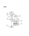
図1に電動駆動制御装置全体の概略を示す。電動駆動制御装置はバッテリー1、インバータ2、交流モータ3、直流入力電圧検出器4、U相、V相、W相の各々の電流検出器5、6、7、回転角検出器8、制御回路9、ゲート駆動回路10、そして制御やゲート駆動に必要な電源11で構成されている。
電動駆動制御装置は外部の上位制御装置から、自動車の運転者および自動車の状態に基づいた速度指令もしくはトルク指令を受け、直流電圧検出器4からの直流電圧値vdc、電流検出器5、6、7からのU相、V相、W相のそれぞれの相電流値iu、iv、iw、回転位置検出器8からのモータ回転子の回転位置角に基づき、モータ3が必要な回転トルクを発生するように、ゲート駆動回路を制御し、インバータ回路2からモータに供給されるU相、V相、W相の電流を制御する。
<Description of the operation of the electric drive device and the process of overcurrent generation>
FIG. 1 shows an outline of the entire electric drive control device. The electric drive control device includes a
The electric drive control device receives a speed command or a torque command based on the state of the vehicle driver and the vehicle from an external host control device, and receives the DC voltage value vdc from the
なお、上記の直流電圧値vdc、相電流値iu、iv、iw、および回転位置角は、それぞれ実際は例えば0〜5Vの電圧として各々の検出器から出力され、制御回路9に入力される。
また以下の説明では簡単のために、制御回路9の動作の説明で用いられる、制御回路9に入力される直流電圧値vdc、相電流値iu、iv、iw、回転位置角およびその他の電流値あるいは電圧値は、それぞれこれらの値に対応する例えば0〜5Vの電圧値である。更に後述の制御回路に備えられたマイクロコンピュータ(マイコン)での処理の説明においては、これらの値はそれぞれこれらに対応した0〜5Vの電圧をAD変換したデジタル値である。また更に誤解の生じない場合は、電流値および電圧値をそれぞれ電流および電圧と略記する。
The DC voltage value vdc, the phase current values iu, iv, iw, and the rotational position angle are actually output from each detector as, for example, a voltage of 0 to 5 V and input to the control circuit 9.
In the following description, for the sake of simplicity, the DC voltage value vdc, phase current values iu, iv, iw, rotational position angles and other current values input to the control circuit 9 are used in the description of the operation of the control circuit 9. Or a voltage value is a voltage value of 0-5V, for example corresponding to these values, respectively. Furthermore, in the description of the processing by a microcomputer (microcomputer) provided in the control circuit described later, these values are digital values obtained by AD conversion of voltages corresponding to 0 to 5 V, respectively. Further, when no misunderstanding occurs, the current value and the voltage value are abbreviated as current and voltage, respectively.
インバータ2で用いる大電力トランジスタ(図1のTu+、Tu−、Tv+、Tv−、Tw+、Tw−)は、例えば
連続通電(DC動作)の場合は300[A](コレクタ温度TC=25℃の場合)で連続運転可能であるが、パルス運転であればその倍の600[A]まで通電が可能である。
The high power transistors (Tu +, Tu−, Tv +, Tv−, Tw +, Tw− in FIG. 1) used in the
インバータに用いる大電力トランジスタは高価であり、近年ではこれらをマイクロコンピュータ(マイコン)により制御し、各種保護を行うことが一般的である。また、自動車用途の主モータの駆動には、多くの場合、電流制御装置が実装される。そこで、インバータの過電流状態もマイコンを用いて、このマイコンの制御サイクルでサンプリング検出し、処理されている。 High-power transistors used in inverters are expensive, and in recent years, it is common to control them with a microcomputer to perform various protections. In many cases, a current control device is mounted to drive a main motor for automobile use. Therefore, the overcurrent state of the inverter is also detected and processed in the microcomputer control cycle using the microcomputer.
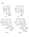
また、インバータを確実に保護するために、あらかじめ設定した電流の閾値(例えば、600[A])により、ゲート信号をオフにする保護機能をインバータのゲート駆動回路に設ける。電流は制御用のものではなく。図2(a)に示すような直流電源のマイナス側のラインに設けたシャント抵抗や、数百[A]以上になる場合には、図2(b)に示すトランジスタにマルチエミッタを設け、主電流を分流し、その分流電流をシャント抵抗で検出するものや、図2(c)に示すトランジスタのコレクタ・エミッタ電圧を検出し、トランジスタオン時のコレクタ電流に対する飽和電圧特性に基づき、間接的に主電流を検出する方式が採用できる。
その検出値と所定のレベルをコンパレータで比較し、その判定結果に応答して、トランジスタのゲートをオフする。
Further, in order to reliably protect the inverter, a protection function for turning off the gate signal according to a preset current threshold (for example, 600 [A]) is provided in the gate drive circuit of the inverter. The current is not for control. When the shunt resistance provided on the negative line of the DC power source as shown in FIG. 2A or more than several hundreds [A] is used, a multi-emitter is provided in the transistor shown in FIG. The current is shunted and the shunt resistance is detected by a shunt resistor, or the collector-emitter voltage of the transistor shown in FIG. 2 (c) is detected, and indirectly based on the saturation voltage characteristics with respect to the collector current when the transistor is on. A method of detecting the main current can be adopted.
The detected value is compared with a predetermined level by a comparator, and the gate of the transistor is turned off in response to the determination result.
図1に示すように、インバータ2は、3アームで構成される。1アームとは通常、2つのトランジスタ、2つのダイオードで構成され、1つのトランジスタのコレクタはバッテリーのプラス側に接続され、エミッタは他方のトランジスタのコレクタに接続されている。そして、他方のトランジスタのエミッタはバッテリーのマイナス側に接地される。2つのダイオードは、2つのトランジスタにそれぞれ接続され、アノードはエミッタにカソードはコレクタに並列接続される。
As shown in FIG. 1, the
1アームの2つのトランジスタは排他的にオンされ、また、トランジスタのオフにかかる遅延時間中の上下短絡を防止するために、オフからオンへの切り替えに遅延時間を設ける。以下本発明の説明にあるPWM出力信号はこれらの処理を行っているとする。 Two transistors in one arm are exclusively turned on, and a delay time is provided for switching from off to on in order to prevent a vertical short circuit during the delay time for turning off the transistor. Hereinafter, it is assumed that the PWM output signal in the description of the present invention performs these processes.
インバータ2にはスイッチングに伴う電流リプルを吸収するC0コンデンサ12(以降、主コンデンサと呼ぶ)とノイズ除去を目的にするC1コンデンサ13、C2コンデンサ14が直流入力側に接続されている。C0コンデンサ12ならびに、直列接続されたC1コンデンサ13とC2コンデンサ14(以降、C1コンデンサとC2コンデンサを合わせてYコンデンサと呼ぶ)は夫々バッテリーのプラス、マイナス端子間に並列に接続される。そして、C1コンデンサ13とC2コンデンサ14の直列接続点Kはシャーシなどに接地される。
The
モータ3は鉄心に3相の巻線が施された固定子を有し、各相巻線の一端は各々Y接続で接続され、他端がインバータ2を構成する各アームのトランジスタのエミッタとコレクタの接続点へ接続される。また、モータは固定子と所定のギャップを設けて回転する、回転子を有している。詳細は省略するが、回転子には誘導モータの場合は、2次巻線を有し、同期モータの場合は、永久磁石を有していて、固定子巻線の通電電流との間に発生する電磁力によりトルクを発生する。
このため、交流出力電流、すなわち、モータ巻線電流と回転子の位置角を検出し、制御回路9によりインバータ2の出力電流制御を行うことで、モータが所定の駆動力を発生するようにU相、V相、W相の電流を供給する。
The
Therefore, the AC output current, that is, the motor winding current and the rotor position angle are detected, and the control circuit 9 controls the output current of the
上記では、インバータがモータを駆動する電流を供給することについて説明したが、自動車の減速時においてモータを発電機として使用する(エネルギー回生する)場合は、このインバータはバッテリーに蓄電する電流を供給する。バッテリーへの蓄電はバッテリーの充放電を制御する別の制御回路(不図示)によって行われ、ここではその説明は省略する。 In the above description, the inverter supplies the current for driving the motor. However, when the motor is used as a generator (regenerative energy) during deceleration of the automobile, the inverter supplies the current stored in the battery. . Power storage in the battery is performed by another control circuit (not shown) that controls charging / discharging of the battery, and the description thereof is omitted here.
図3は本発明を実施するための制御回路9の1つの例をブロック図で示している。
この制御回路9は相電流値および直流電圧値の振幅が所定の値を超える場合は異常と判定し、ゲート駆動回路にインバータのトランジスタのゲート信号をオフさせて、トランジスタを保護する、過電流保護機能を実装している。
FIG. 3 is a block diagram showing an example of the control circuit 9 for carrying out the present invention.
The control circuit 9 determines that an abnormality occurs when the amplitude of the phase current value and the DC voltage value exceeds a predetermined value, and causes the gate drive circuit to turn off the gate signal of the transistor of the inverter, thereby protecting the transistor. The function is implemented.
図3の制御回路9において、核になるマイクロコンピュータ(マイコン)39は図1に示した制御回路に実装されている。各相電流検出器の出力(相電流値)は、ヒステリシスコンパレータ20に入力されるとともに、マルチプレクサ&サンプルホールド32(サンプリング回路)を介してマイコン39のADコンバータ19に入力される。また、直流電圧検出器4からの出力(直流電圧値)はマルチプレクサ&サンプルホールド32を介してマイコン39のADコンバータに入力される。
In the control circuit 9 of FIG. 3, a
マイコン39は周期毎に、マルチプレクサ&サンプルホールド32を介して上記の相電流値および直流電圧値をサンプリングし、後述するように、インバータの電流制御を行うとともに、相電流値の振幅が所定の値を超える場合は異常と判定し、過電流保護処理を行う。
The
前述のように出力電流の制御は、制御回路9内のマイコン39により、例えば、図4に示すフローチャートの処理により実行される。そして、この処理はインバータのパルス幅変調(以降、PWMと記す)のキャリア周期毎に実行される。
As described above, the control of the output current is executed by the
以下図4を参照して、本発明の実施形態でも使用されるインバータの電流制御について説明する。
処理が開始するとステップS801で、他処理で演算し、記憶されたd軸および、q軸電流指令id*、iq*をメモリより読み込む。ステップS802で3相の出力電流iu、iv、iw(図1参照)のAD変換結果を、ステップS803で直流電圧vdcを、それぞれ所定のレジスタより読み込む。そして、ステップS804において、回転角θをマイコン39の外部メモリデータバス25に接続されたRDコンバータから読み込む。
Hereinafter, with reference to FIG. 4, the current control of the inverter used also in the embodiment of the present invention will be described.
When the process starts, in step S801, the calculation is performed in another process, and the stored d-axis and q-axis current commands id * and iq * are read from the memory. In step S802, the AD conversion results of the three-phase output currents iu, iv, iw (see FIG. 1) are read from the predetermined registers, and in step S803, the DC voltage vdc is read from the predetermined register. In step S804, the rotation angle θ is read from the RD converter connected to the external
ステップS805において、後で説明する過電流保護処理をコールし、そこから復帰するとステップS806に進む。ステップS806では、読み込んだ3相電流(iu、iv、iw)および、回転角θによりd−q座標変換し、d軸、q軸電流(id、iq)を求める。次に、ステップS807において、d軸、q軸のそれぞれの指令電流より実電流を減算し、電流偏差(ed、eq)を算出し、ステップS808において、d軸、q軸のそれぞれの電流偏差に対して、次式のPI演算処理を実施し、d軸、q軸電圧指令を算出する。
vd=Kpd・ed+Kid{ed+ed0} ...(1)
vq=Kpq・eq+Kiq{eq+eq0}
ここで、Kpd、Kpqはそれぞれd軸、q軸の比例ゲイン、Kid、Kiqはd軸、q軸の積分ゲインである。またed、eqはそれぞれd軸、q軸の電流偏差であり、ed0、eq0はそれぞれ1サンプル前(このフローチャートに示す処理を前周期に実行した時)のd軸、q軸の電流偏差である。
In step S805, an overcurrent protection process, which will be described later, is called, and after returning from it, the process proceeds to step S806. In step S806, d-q coordinate conversion is performed using the read three-phase current (iu, iv, iw) and the rotation angle θ to obtain d-axis and q-axis currents (id, iq). Next, in step S807, the actual current is subtracted from the d-axis and q-axis command currents to calculate current deviations (ed, eq). In step S808, the current deviations in the d-axis and q-axis are calculated. On the other hand, PI calculation processing of the following equation is performed to calculate d-axis and q-axis voltage commands.
vd = Kpd · ed + Kid {ed + ed0}. . . (1)
vq = Kpq · eq + Kiq {eq + eq0}
Here, Kpd and Kpq are the d-axis and q-axis proportional gains, and Kid and Kiq are the d-axis and q-axis integral gains, respectively. In addition, ed and eq are current deviations of the d-axis and q-axis, respectively, and ed0 and eq0 are current deviations of the d-axis and q-axis one sample before (when the processing shown in this flowchart is executed in the previous cycle), respectively. .
ステップS809において、電流偏差(ed、eq)を今回のサンプル値として記憶(ed0、ed0)する。ステップS810において、得られたd軸、q軸電圧指令(vd、vq)を、回転角θに基づいて3相電圧(vu*、vv*、vw*)に変換する。そして、この電圧指令をステップS811 において、直流入力電圧vdcおよび、PWMのキャリア周期Tcにより次式でパルス幅(tu、tv、tw)に変換する。
tu=Tc・(1+vu*/vdc)/2 ...(2)
tv=Tc・(1+vv*/vdc)/2
tw=Tc・(1+vw*/vdc)/2
In step S809, the current deviation (ed, eq) is stored (ed0, ed0) as the current sample value. In step S810, the obtained d-axis and q-axis voltage commands (vd, vq) are converted into three-phase voltages (vu * , vv * , vw * ) based on the rotation angle θ. In step S811, the voltage command is converted into a pulse width (tu, tv, tw) by the following equation using the DC input voltage vdc and the PWM carrier cycle Tc.
tu = Tc · (1 + vu * / vdc) / 2. . . (2)
tv = Tc · (1 + vv * / vdc) / 2
tw = Tc · (1 + vw * / vdc) / 2
ステップS812において、各相パルス幅が0〜Tcの範囲になるようにクランプする。具体的には、パルス幅が負の場合は0に、Tcを越えた場合はTcにパルス幅を変更する。この結果をマイコン39のPWMタイマにステップS813においてセットし、処理を終了し、図示を省略したメインの処理に復帰する。
In step S812, clamping is performed so that each phase pulse width is in the range of 0 to Tc. Specifically, the pulse width is changed to 0 when the pulse width is negative, and to Tc when the pulse width exceeds Tc. The result is set in the PWM timer of the
次に過電流保護処理について説明する。
図5を参照して従来の過電流検出のフローチャートを説明する。この処理が開始すると、図4のステップS802で読み込んだ3相電流をステップS91において所定レベル(閾値)と比較する。電流がこの所定レベルを超えた場合には、過電流と判定し、ステップS92において、カウンタCをインクリメントする。電流が所定レベル以下の場合は、ステップS93において、カウンタをゼロにセットする。ステップS94において、カウンタが所定カウント値に達したかを判定し、所定カウント値を超えた場合には、ステップS95において、インバータの全トランジスタ素子をオフし、ステップS96で過電流異常フラグをセットし、ステップS97で復帰する。カウンタが所定カウント以下の場合は、ステップS97で復帰する。過電流異常フラグがセットされた場合には、その他の処理(図示省略)にて、所定の手続きで、再スタート可の判定により、過電流異常フラグがクリアされるまで、図4のフローチャート処理は停止する。
異常がない場合は、図4に示すフローチャートの一連の処理によりインバータ出力電流は所定の指令電流に制御される。
Next, the overcurrent protection process will be described.
A conventional overcurrent detection flowchart will be described with reference to FIG. When this process starts, the three-phase current read in step S802 in FIG. 4 is compared with a predetermined level (threshold value) in step S91. If the current exceeds the predetermined level, it is determined that the current is an overcurrent, and the counter C is incremented in step S92. If the current is below the predetermined level, the counter is set to zero in step S93. In step S94, it is determined whether the counter has reached a predetermined count value. If the predetermined count value is exceeded, all the transistor elements of the inverter are turned off in step S95, and an overcurrent abnormality flag is set in step S96. In step S97, the process returns. If the counter is less than or equal to the predetermined count, the process returns at step S97. When the overcurrent abnormality flag is set, the flowchart process of FIG. 4 is performed until the overcurrent abnormality flag is cleared by determining whether restart is possible in a predetermined procedure in other processing (not shown). Stop.
If there is no abnormality, the inverter output current is controlled to a predetermined command current through a series of processes in the flowchart shown in FIG.
図6は、過電流を引き起こす上記故障モード、1)出力地絡/天絡、2)出力線間短絡、3)出力相間短絡の回路状態の例をそれぞれ示す。なお、簡単のため、図6ではこれらの故障モードの1つの例において関係するインバータの部分のみを示している。複数の箇所および複数のアーム部分が関連するような故障も考えられるが、ここでは省略している。 FIG. 6 shows examples of circuit states of the failure mode causing overcurrent, 1) output ground fault / power fault, 2) output line short circuit, and 3) output phase short circuit. For the sake of simplicity, FIG. 6 shows only the portion of the inverter related in one example of these failure modes. Although a failure involving a plurality of locations and a plurality of arm portions is also conceivable, it is omitted here.
図6(a)は、U相のアーム上側のトランジスタがオンになっている場合の地絡による電流の流れを示す。出力地絡の一例について少し詳細に説明する。 FIG. 6A shows a current flow due to a ground fault when the transistor on the upper side of the U-phase arm is turned on. An example of the output ground fault will be described in some detail.
[出力地絡]
図7(a)は出力地絡の等価回路である。この等価回路は、Yコンデンサ(C1=C2とする)、主コンデンサC0そして地絡点までの配線の抵抗51(r)、インダクタンス52(L)のLCR直列回路として示されている。そして、抵抗値は十分小さく、また、C0に比べ、C1は十分小さいので、r2−4L/C<0の条件が成り立ち、この直列回路には、下記の(3)式で示す周波数fcの共振電流が流れる。
fc=(1/(L・2・C1)−(r/(2L))2)0.5/2π [Hz]
...(3)
そして、そのピーク電流ipeakは、コンデンサの初期電圧をVとすれば、
ipeak=2V/((4L−r2)/(2・C1))0.5[A]
...(4)
で与えられる。
ここで、インバータの入力直流電圧vdc=350[V](C1の初期電圧Vはこの半分であり、175[V])とし、インバータからモータへの1相分の配線抵抗r=1[mΩ]、インダクタンスL=0.5[μH]、主コンデンサC0=900[μF]、Yコンデンサ=1[μF]とすると、その周波数は159[kHz]になり、ピーク電流は495[A]となる。
[Output ground fault]
FIG. 7A is an equivalent circuit of an output ground fault. This equivalent circuit is shown as an LCR series circuit of a Y capacitor (C1 = C2), a main capacitor C0, a resistance 51 (r) of wiring to the ground fault point, and an inductance 52 (L). Since the resistance value is sufficiently small and C1 is sufficiently small compared to C0, the condition r 2 −4L / C <0 is satisfied, and this series circuit has a frequency fc expressed by the following equation (3). Resonant current flows.
fc = (1 / (L · 2 · C1) − (r / (2L)) 2 ) 0.5 / 2π [Hz]
... (3)
And the peak current ipeak is given by V as the initial voltage of the capacitor.
peak = 2V / ((4L−r 2 ) / (2 · C1)) 0.5 [A]
... (4)
Given in.
Here, the inverter input DC voltage vdc = 350 [V] (the initial voltage V of C1 is half of this, 175 [V]), and the wiring resistance r = 1 [mΩ] for one phase from the inverter to the motor When the inductance L = 0.5 [μH], the main capacitor C0 = 900 [μF], and the Y capacitor = 1 [μF], the frequency is 159 [kHz] and the peak current is 495 [A].
このような電流の周波数は、従来のマイクロプロセッサ(マイコン)を用いた制御方法において、マイコンの制御周波数(=電流検出の周波数)で行うサンプリングの周波数より10倍以上高く、従ってマイコンでの検知は難しい。更に、この電流が、ゲート駆動回路に通常用いられる保護回路の過電流検知レベル(この実施例では600[A])よりも低いこと、また、インバータのトランジスタのスイッチングが途中で行われても、図7(b)から 図7(c)への電流経路(図中の矢印)が形成され、図7(a)の等価回路での過渡現象が、スイッチング毎に生じるため、持続的にこの振動電流が流れる。そして、この電流は、たとえば、連続定格300[A]を超えている。 The frequency of such current is more than 10 times higher than the sampling frequency performed at the control frequency (= current detection frequency) of the microcomputer in the control method using the conventional microprocessor (microcomputer). difficult. Furthermore, even if this current is lower than the overcurrent detection level (600 [A] in this embodiment) of the protection circuit normally used for the gate drive circuit, and even if switching of the transistor of the inverter is performed halfway, A current path (arrow in the figure) from FIG. 7B to FIG. 7C is formed, and a transient phenomenon in the equivalent circuit of FIG. Current flows. This current exceeds, for example, a continuous rating of 300 [A].
次に、地絡以外の場合では天絡、線間短絡および相間短絡があるが、図6(b)、(c)と(d)でそれぞれ示すように、天絡、線間短絡および相間短絡では短絡電流の経路および動作が類似している。これらは、インバータ出力線間のインピーダンスが低下することと等価であり、共振周波数も同様に計算できるので、以下では線間短絡について少し詳しく説明する。 Next, in cases other than ground faults, there are power faults, line-to-line shorts, and phase-to-phase shorts, but as shown in FIGS. 6 (b), (c) and (d), respectively, The short-circuit current path and operation are similar. These are equivalent to a decrease in the impedance between the inverter output lines, and the resonance frequency can be calculated in the same manner. Therefore, the line short circuit will be described in a little more detail below.
[線間短絡]
図8は、図6(c)で示した線間短絡の場合の電流の流れを示す。ここではU相巻線とV相巻線の間で線間短絡が起こったとして示してある。なお、簡単のため、インバータの関係する部分のみ示している。トランジスタはU相、V相、W相いずれでもよいので、この線間短絡に関わるトランジスタをSWa、SWb、Sp、Snでとして図示している。
[Short-circuit between lines]
FIG. 8 shows a current flow in the case of the line short-circuit shown in FIG. Here, it is shown that a line short circuit has occurred between the U-phase winding and the V-phase winding. For simplicity, only the portion related to the inverter is shown. Since the transistor may be any of the U phase, the V phase, and the W phase, the transistors related to this short circuit between lines are illustrated as SWa, SWb, Sp, and Sn.
主コンデンサ12(C0)、そして、短絡点までの配線の抵抗53(rs)、インダクタンス54(Ls)とすれば、共振周波数fcsは
fcs=(1/(Ls・C0)−(rs/(2Ls))2)0.5/(2π)[Hz] ...(5)
となる。仮に、Lsを5[μH]として、前述と同じ回路定数を用い共振周波数を求めると2.4[kHz]になる。インバータのPWM周期を10[kHz]とすると、例えば、共振の1周期に図8(a)のトランジスタSWaは4回スイッチングする。
If the main capacitor 12 (C0), the resistance 53 (rs) of the wiring to the short circuit point, and the inductance 54 (Ls) are used, the resonance frequency fcs is fcs = (1 / (Ls · C0) − (rs / (2Ls)). )) 2 ) 0.5 / (2π) [Hz]. . . (5)
It becomes. If Ls is 5 [μH] and the resonance frequency is obtained using the same circuit constant as described above, it becomes 2.4 [kHz]. If the PWM period of the inverter is 10 [kHz], for example, the transistor SWa in FIG.
ここで、上述した条件で、短絡直後の電流応答を図9に模式的に示す。なお、図中、トランジスタSpはオンしているものとする。図中の実電流の波形が期間Iと期間IIとでやや異なるのは以下の理由による。 Here, the current response immediately after the short circuit is schematically shown in FIG. 9 under the above-described conditions. In the figure, it is assumed that the transistor Sp is on. The actual current waveform in the figure is slightly different between the period I and the period II for the following reason.
期間I:指令電流に対し、実電流が大きくオーバーシュートするため、電流制御が実行されて、図8(a)のトランジスタSWaのオンDutyが縮小しながらも電流は増加を続ける。ここで、電流をdi=v・dt/Ls(vは短絡端子間の電圧)で表すとき、電流の変化は、インダクタンス54Lsがモータの巻線のインダクタンスに比べ小さいため大きくなり、そのため、オーバーシュートを引き起こす。
なお、図8(a)の中で、実線の矢印がトランジスタSWaオン時の電流経路(直流電圧が短絡線間に印加)、破線の矢印がトランジスタSWaオフ時の電流経路(ゼロ電圧が短絡線間に印加)を示している。
Period I: Since the actual current greatly overshoots the command current, current control is executed, and the current continues to increase while the ON duty of the transistor SWa in FIG. 8A is reduced. Here, when the current is expressed by di = v · dt / Ls (v is the voltage between the short-circuit terminals), the change in the current is large because the inductance 54Ls is smaller than the inductance of the motor winding, and therefore the overshoot. cause.
In FIG. 8A, the solid line arrow indicates the current path when the transistor SWa is on (DC voltage is applied between the short-circuit lines), and the broken line arrow indicates the current path when the transistor SWa is off (zero voltage is the short-circuit line). (Applied between).
時刻ts:コイル(rs、Ls)に印加する電圧指令が負に反転したため、図8(b)のトランジスタSWbによるスイッチング(オン・オフ)に切り替わる。そして、トランジスタSnがオンする。
期間II:コイルのLsが通常より小さくなっているため、電流制御により図8(b)のトランジスタSWbのDutyが調整されても、指令電流に対し、実電流は大きくアンダーシュートする。
なお、図8(b)の中で、実線の矢印がトランジスタSWbオン時の電流経路(直流電圧が短絡線間に印加)、破線の矢印がトランジスタSWbオフ時の電流経路(ゼロ電圧が短絡線間に印加)を示している。
Time ts: Since the voltage command to be applied to the coils (rs, Ls) is inverted negatively, switching is performed (ON / OFF) by the transistor SWb in FIG. 8B. Then, the transistor Sn is turned on.
Period II: Since the Ls of the coil is smaller than usual, even if the duty of the transistor SWb in FIG. 8B is adjusted by current control, the actual current greatly undershoots the command current.
In FIG. 8B, the solid line arrow indicates the current path when the transistor SWb is on (DC voltage is applied between the shorted lines), and the broken line arrow indicates the current path when the transistor SWb is off (zero voltage is the shorted line). (Applied between).
図9の鋸状の実電流波形は、インピーダンス低下に伴い電流制御系のゲインが相対的に高くなり、制御が発振している状態と解釈することもできる。
また、上述したとおり、制御に使う電流検出器の検出範囲は、電流制御が機能することを前提に選定されるので、オーバーシュートもしくはアンダーシュートが大きいと、検出値はクランプされてしまい、更に、制御系は発振的動作に陥る。
もっとも、地絡の場合に比べ、周波数が低いため、検知範囲を超えない領域で、電流はマイコンにて正しくサンプリングが可能であり、また、この検知により電流がクランプしたことも判定はできる。しかし、マイコンの通常の過電流検知アルゴリズムでは、過電流を検知できない場合がある。
以下に従来の過電流検知方法を説明し、次にこれを改善する本発明の過電流検知装置およびこれを用いた検知方法を説明する。
The sawtooth actual current waveform in FIG. 9 can be interpreted as a state in which the control is oscillating because the gain of the current control system becomes relatively high as the impedance decreases.
In addition, as described above, the detection range of the current detector used for control is selected on the assumption that the current control functions, so if the overshoot or undershoot is large, the detection value is clamped, The control system falls into oscillating operation.
However, since the frequency is lower than in the case of a ground fault, the current can be correctly sampled by the microcomputer in a region that does not exceed the detection range, and it can also be determined that the current has been clamped by this detection. However, the normal overcurrent detection algorithm of the microcomputer may not be able to detect overcurrent.
A conventional overcurrent detection method will be described below, and then an overcurrent detection device of the present invention for improving this and a detection method using the same will be described.
[従来の過電流検出方法]
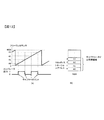
マイコンを用いた通常の過電流検知アルゴリズムでは、誤検知を解消するため、タイムウィンドウを設ける。これは、具体的には、所定のサンプル回数連続して過電流を検知した場合に、異常を確定するものである(図5のフローチャート参照)。
[Conventional overcurrent detection method]
In a normal overcurrent detection algorithm using a microcomputer, a time window is provided to eliminate erroneous detection. Specifically, when an overcurrent is detected continuously for a predetermined number of times, an abnormality is determined (see the flowchart of FIG. 5).
しかしながら、例えば図10に例示するように、このマイコンを用いた通常の過電流検知アルゴリズムでは、過電流が判定できないことがある。ここでは、10[kHz]にて電流制御と過電流判定を行うシステムを想定している。このシステムは、線間短絡異常で発振周波数が2.5[kHz]、振幅450[A]の電流が流れた場合、タイムウィンドウとして、電流が閾値を3回連続で越えた場合、過電流と判定するように設計されている。図10では正側の過電流が連続2回、負側の過電流が連続2回検出されているが、連続3回の過電流検出の条件を満たしていないため、過電流と判断されない。なお、図10の正側の過電流検出点i1、i2、および負側の過電流検出点i4、i5はそれぞれ、クランプされた電流値が検出されたことを示している。 However, as exemplified in FIG. 10, for example, an overcurrent may not be determined by a normal overcurrent detection algorithm using this microcomputer. Here, a system that performs current control and overcurrent determination at 10 [kHz] is assumed. In this system, when a current with an oscillation frequency of 2.5 [kHz] and an amplitude of 450 [A] flows due to an abnormal short circuit between lines, as a time window, when the current exceeds a threshold value three times in succession, an overcurrent is detected. Designed to judge. In FIG. 10, the positive overcurrent is detected twice consecutively and the negative overcurrent is detected twice consecutively. However, since the condition of three consecutive overcurrent detection is not satisfied, it is not determined as an overcurrent. Note that the positive-side overcurrent detection points i1 and i2 and the negative-side overcurrent detection points i4 and i5 in FIG. 10 indicate that clamped current values are detected, respectively.
このように過電流が判断されない場合には、継続的な発振電流の通電を許し、ひいては、素子破壊に至る不具合が発生する可能性がある。
また、天絡についても同様に、インバータ出力端のインピーダンスが極めて小さくなるため、電流制御の発振を引き起こす可能性がある。
If overcurrent is not determined in this way, continuous oscillation current may be allowed to flow, leading to the possibility of a failure leading to element destruction.
Similarly, for the power supply, the impedance of the inverter output terminal is extremely small, which may cause current control oscillation.
したがって、実施形態の過電流検出装置では、上記の3つの故障モードにより発生する大振幅な高周波電流の周波数もしくは、周期を検出して、過電流を判定するアルゴリズムを搭載する。すなわち、実施形態の過電流検出装置は、電流振幅が予め定めた閾値を越えたときに過電流を判定するアルゴリズムに加えて、周波数もしくは周期検出アルゴリズムも実装している。 Therefore, the overcurrent detection device of the embodiment is equipped with an algorithm for detecting an overcurrent by detecting the frequency or period of a large-amplitude high-frequency current generated by the three failure modes. That is, the overcurrent detection device according to the embodiment implements a frequency or period detection algorithm in addition to an algorithm for determining overcurrent when the current amplitude exceeds a predetermined threshold.
以下に本発明による過電流検出装置および過電流検出方法を説明する。 The overcurrent detection device and overcurrent detection method according to the present invention will be described below.
[実施形態1]
図3で既に説明したように、各相電流検出器の出力は、マイコン39のADコンバータ19に入力するとともに、ヒステリシスコンパレータ20に入力される。ヒステリシスコンパレータ20のヒステリシス幅は大振幅の振動電流をパルス変換するために、例えば、連続定格300[A]のトランジスタを使う場合、100[A]程度に設定する。そして、このコンパレータ20の出力はマイコン39の外部パルスカウンタ21、22および23の各端子に接続される。これらのパルスカウンタ21、22および23は、パルスの立ち上がりエッジでカウントアップするように、図示を省略する他の処理で初期設定している。
[Embodiment 1]
As already described with reference to FIG. 3, the output of each phase current detector is input to the
また、モータ3の電流やトルクを制御するために、直流電圧検出器4の出力がADコンバータ19に入力され、回転位置検出器(レゾルバ)8の信号を角度に変更するRDコンバータ24がマイコン39の外部バス25に接続されている。マイコン39内のPWMタイマ26、27および28)はインバータ2を構成する各相のトランジスタのオン時間がセットされ、マイコン39は、ゲート駆動回路10へPWM信号を出力する。各相のトランジスタのオン時間はCPU31で演算される。各相のPWMタイマ26、27および28へは共通のキャリア(fc)タイマ29が接続されており、各相におけるPWMのキャリア周期を生成している。そして、キャリア周期毎に狭パルス(例えば、パルス“1”の幅1[μs])を出力するとともに、ADコンバータ19での変換を開始するとともに、マルチプレクサ&ホールド32(サンプリング回路)により、この入力を逐次切り替えてサンプリングし、各相電流(iu、iv、iw)並びに直流電圧vdcを、対応するレジスタに格納するように、図示を省略する他の処理で初期設定している。
In order to control the current and torque of the
[過電流検出処理]
図11は本発明による過電流検出処理のフローチャートである。このフローチャートは所定の周期で実行される。本実施形態では過電流検出処理は電流制御処理の実行毎に、図4のステップS805においてコールされる。まず、図11のフローチャートのステップS501〜S504までの処理により、電流の振幅と閾値の比較により、過電流を判定する処理を実行する。次に、ステップS505において、カウンタ値Fkを上記ヒステリシスコンパレータが接続された外部パルスカウンタから読み込む。読み込み完了と同時にステップS506でカウンタをクリアする。
[Overcurrent detection processing]
FIG. 11 is a flowchart of the overcurrent detection process according to the present invention. This flowchart is executed at a predetermined cycle. In this embodiment, the overcurrent detection process is called in step S805 of FIG. 4 every time the current control process is executed. First, a process of determining an overcurrent is performed by comparing the amplitude of the current with a threshold value by the processes of steps S501 to S504 in the flowchart of FIG. In step S505, the counter value Fk is read from the external pulse counter to which the hysteresis comparator is connected. Simultaneously with the completion of reading, the counter is cleared in step S506.
仮に本処理が100[μs](=電流制御処理)毎に実行されているとすると、Fk=1は、1/100[μs]=10[kHz]となる。すなわち、パルスの周波数FPk[Hz] は、処理実行周期をTsampl[s]とすれば
FPk=Fk/Tsampl ...(6)
により、周波数に換算できる。また、判定するカウンタ閾値Flimitは、周波数の閾値をFPlimit[Hz]とすれば、
Flimit=FPlimit・Tsampl ...(7)
と設定できる。
If this process is executed every 100 [μs] (= current control process), Fk = 1 is 1/100 [μs] = 10 [kHz]. That is, the pulse frequency FPk [Hz] is FPk = Fk / Tsampl..., If the processing execution cycle is Tsampl [s]. . . (6)
Can be converted to a frequency. Further, the counter threshold Flimit to be determined is FPlimit [Hz] as a frequency threshold.
Flimit = FPlimit · Tsampl. . . (7)
Can be set.
ステップS507で、カウンタ値Fkと過電流判定のカウンタ閾値Flimitを比較する。閾値を越えていた場合は、ステップS508において、インバータの全トランジスタ素子をオフし、ステップS509で過電流異常フラグをセットし、ステップS510で復帰する。カウンタ値が所定カウンタ閾値以下の場合は、ステップS510で復帰する。過電流異常フラグがセットされた場合、図示を省略したその他処理にて、所定の手続きで、再スタート可の判定により、過電流異常フラグがクリアされるまで、図4のフローチャート処理は停止する。 In step S507, the counter value Fk is compared with the counter threshold value Flimit for overcurrent determination. If the threshold value is exceeded, all transistor elements of the inverter are turned off in step S508, an overcurrent abnormality flag is set in step S509, and the process returns in step S510. If the counter value is less than or equal to the predetermined counter threshold, the process returns in step S510. When the overcurrent abnormality flag is set, the flowchart processing of FIG. 4 stops until the overcurrent abnormality flag is cleared by determining whether restart is possible in a predetermined procedure in other processing not shown.
なお、例えば、線間短絡のような故障モードでは、振動する過電流の周波数が電流制御周期より低い場合があるので、ステップS505〜ステップS509の処理を電流制御周期とは別の周期、例えば、10[ms]で実行しても良い。 Note that, for example, in a failure mode such as a short circuit between lines, the frequency of the oscillating overcurrent may be lower than the current control cycle, so the processing of step S505 to step S509 is a cycle different from the current control cycle, for example, It may be executed in 10 [ms].
車両用インバータで使われるインバータのYコンデンサを2[μF]以下、インバータよりモータまでの配線の長さを10[m]以下で、その抵抗、インダクタンスはそれぞれ、1[mΩ]、1[μH]以下とし、配線端で地絡した場合を想定すると、式(3)により、共振周波数は113[kHz]となる。故に、FPlimitとして、113[kHz]を採用することができる。 The inverter Y capacitor used in the vehicle inverter is 2 [μF] or less, the length of the wiring from the inverter to the motor is 10 [m] or less, and its resistance and inductance are 1 [mΩ] and 1 [μH], respectively. Assuming the case where a ground fault occurs at the wiring end, the resonance frequency is 113 [kHz] according to the equation (3). Therefore, 113 [kHz] can be adopted as FPlimit.
また、線間短絡や相間短絡を検知したい場合は、例えば、マイコンの電流制御周期(電流検出の周期)に鑑み設定する。例えば、電流検出の周期が100[μs]であれば、その10倍の周期はマイコンの電流検出に基づく過電流判定が十分行われないとして、FPlimitとして、1[kHz]を採用することができる。この設定値は、地絡の場合に観測される周波数より低いため、地絡の場合を含めて、過電流を検知することができる。 Further, when it is desired to detect a short circuit between lines or a short circuit between phases, for example, it is set in consideration of the current control cycle (current detection cycle) of the microcomputer. For example, if the period of current detection is 100 [μs], it is possible to adopt 1 [kHz] as the FPlimit because the overcurrent determination based on the current detection of the microcomputer is not sufficiently performed for 10 times the period. . Since this set value is lower than the frequency observed in the case of a ground fault, overcurrent can be detected including the case of a ground fault.
なお、地絡、線間短絡や相間短絡における過電流の周波数は式(3)または式(5)の演算で求めることができる。しかし、それら故障モードでは、式中、1/(L・2・C1)≫(r/(2L))2、もしくは、1/(Ls・C0)≫(rs/(2Ls))2の関係が成立するので、
fc=(1/(L・2・C1))0.5 /(2π)[Hz] ...(8)
または、
fcs=(1/(Ls・C0))0.5 /(2π) [Hz] ...(9)
のように計算式を簡略化でき、これに基づいて上記周波数を算出してもよい。
In addition, the frequency of the overcurrent in a ground fault, a line short circuit, and a phase short circuit can be calculated | required by the calculation of Formula (3) or Formula (5). However, in these failure modes, the
fc = (1 / (L · 2 · C1)) 0.5 / (2π) [Hz]. . . (8)
Or
fcs = (1 / (Ls · C0)) 0.5 / (2π) [Hz]. . . (9)
Thus, the calculation formula can be simplified, and the frequency may be calculated based on this.
しかしながら、例えば、8極対のモータを採用し、10,000[rpm]までモータ駆動するシステムでは、インバータ出力の基本波電流の周波数が1.333[kHz](=(10000/60)×8)に達するため、0を中心にヒステリシス幅を持つコンパレータでは、正常時においても過電流と検知する不都合が生じる。 However, for example, in a system that employs an 8-pole motor and drives the motor up to 10,000 [rpm], the frequency of the fundamental wave current of the inverter output is 1.333 [kHz] (= (10000/60) × 8 ), A comparator having a hysteresis width centered on 0 causes the inconvenience of detecting an overcurrent even during normal operation.
これを解消するためには、インバータの基本波電流を中心にヒステリシス幅を持つコンパレータを採用すればよい。たとえば、ヒステリシス中心値変更回路を備えたタイプ2(図16(b))を採用することができる。この方式については実施形態3で説明する。また、減算回路を備えたタイプ3(図16(c))のヒステリシスコンパレータを採用することもできる。
In order to solve this problem, a comparator having a hysteresis width around the fundamental wave current of the inverter may be employed. For example, Type 2 (FIG. 16B) having a hysteresis center value changing circuit can be employed. This method will be described in
[実施形態2]
図12は、本発明による制御回路のもう1つの実施形態のブロック図を示している。これは、マイコン内のカウンタ21、22および23)に代えて、(1)3つのキャプチャ34、35および36)端子に各相コンパレータ出力をそれぞれ接続する。(2)計時用のフリーランカウンタ37を追加する。(3)キャプチャ毎にデータを所定のRAM領域に転送するDMAコントローラ38を追加する。
[Embodiment 2]
FIG. 12 shows a block diagram of another embodiment of a control circuit according to the present invention. In this case, instead of the
キャプチャは、図13に示すように、端子に入力されたパルスの立上り、立下りエッジ(両エッジ)にて、フリーランカウンタ37の値を読み取り、所定のレジスタに転送する。そして、DMAコントローラ38はパルスの両エッジに応答して、所定のRAMアドレスに逐次、そのレジスタの値を転送する。アドレスは、DMAコントローラ38によりデータ転送毎にn[byte]インクリメントされ、指定の停止アドレスまで達すると開始アドレスに初期化され、データ転送毎のインクリメントは続けられる。
As shown in FIG. 13, in the capture, the value of the free-
図13の例では、レジスタに4[byte]データが格納されるとして、計4データ(16[byte])をRAMに転送するとDMAのディストネーションアドレスを開始アドレスへ初期化する(図の場合、アドレス“3”→“0”)ように、DMAコントローラを設定したデータの格納例を示している。 In the example of FIG. 13, assuming that 4 [bytes] data is stored in the register, when a total of 4 data (16 [bytes]) is transferred to the RAM, the DMA destination address is initialized to the start address (in the case of FIG. 13, An example of storing data in which the DMA controller is set as shown in the address “3” → “0”) is shown.
図14は過電流検知のためのフローチャートを示している。これは、電流制御とは異なる所定周期、例えば10[ms]にて実行される。処理を開始すると電流検出値がキャプチャされ、RAMの所定のエリアに格納されたフリーランカウンタ37のカウント値をステップS601で読み込む。この際、隣接するアドレスから2データ(Ak(n)、Ak(n+1))を読み込む。具体的には、図の0番地と1番地、1番地と2番地、2番地と3番地、3番地と0番地、0番地と1番地、...のようにサイクリックに2データを読み出す。
FIG. 14 shows a flowchart for overcurrent detection. This is executed at a predetermined cycle different from the current control, for example, 10 [ms]. When the process is started, a current detection value is captured, and the count value of the free-
ステップS602では2データの差分(パルス周期)を演算する。フローチャートへの詳細記載はしていないが、この際、開始アドレスと終点アドレスの2データを読み込んだ場合は、(開始アドレスのデータ−終点アドレスのデータ)とし、それ以外については、(大きいアドレスのデータ−小さいアドレスのデータ)の処理、すなわち、キャプチャのタイミングが遅いものより早いものを減算処理する。
このようにしてパルスの立ち上がり/立ちさがりの位置が検出され、このパルスの立ち上がり/立ちさがりの位置から、このパルスの周波数が求められる。
In step S602, a difference (pulse period) between the two data is calculated. Although not described in detail in the flowchart, at this time, when two data of the start address and the end address are read, it is set as (start address data-end point address data), and otherwise (the larger address (Data-data at a small address), that is, subtraction processing is performed on the data that is earlier than the one with the later capture timing.
In this way, the rising / rising position of the pulse is detected, and the frequency of the pulse is obtained from the rising / falling position of the pulse.
そして、ステップS603において、計測されたパルス周期と閾値の比較により、過電流を判定する。周期が所定レベル未満の場合には、過電流と判定する。そして、ステップS604において、インバータ2の全トランジスタ素子をオフし、ステップS605で、過電流異常フラグをセットし、ステップS606で復帰する。周期が所定レベル以上の場合は、ステップS606で復帰する。
なお、振幅を検出する従来の方法に基づく、図5のフローチャートで実施される過電流検出処理は、図8の電流制御処理フローチャートのS805にてコールするように設定する。
In step S603, an overcurrent is determined by comparing the measured pulse period with a threshold value. When the period is less than a predetermined level, it is determined that the current is overcurrent. In step S604, all transistor elements of the
Note that the overcurrent detection process performed in the flowchart of FIG. 5 based on the conventional method of detecting the amplitude is set to be called in S805 of the current control process flowchart of FIG.
実施形態1および2の装置によれば、高周波電流のピークが、制御用マイコンに接続される電流検出器の検出範囲を超えてしまう場合、およびクランプにより、真の電流値が読み取れない場合でも、周波数もしくは、周期を用いて過電流を判定するため、過電流を検知できる特有の効果を有する。
According to the devices of
判定するための周期の閾値としては、実施形態1で示した考え方により、判定する周波数の閾値を求め、その逆数を採用すればよい。 As a cycle threshold for determination, a threshold for frequency to be determined may be obtained based on the concept described in the first embodiment, and the reciprocal thereof may be adopted.
図15は、実施形態1または2の過電流検出処理の機能ブロックを1相分示している。実施形態1および2では、電流の振幅に基づく過電流検出部に加えて、電流の周波数もしくは、周期に基づく過電流検出部を備えている。そして、両検出部の出力の論理和に基づき、過電流検出信号を得ることにより、従来は検出が困難であった地絡、相間短絡、あるいは線間短絡に起因した電流異常をも検出することができる。 FIG. 15 illustrates one phase of functional blocks of the overcurrent detection process according to the first or second embodiment. In the first and second embodiments, an overcurrent detection unit based on the frequency or period of the current is provided in addition to the overcurrent detection unit based on the amplitude of the current. And by detecting the overcurrent detection signal based on the logical sum of the outputs of both detectors, it is also possible to detect current faults caused by ground faults, phase shorts, or line shorts that were difficult to detect in the past Can do.
[実施形態3]
図16は、本発明を実施するヒステリシスコンパレータの構成例を1相分示している。電流検知器は、0〜5[V]の出力範囲で、電流0[A]で2.5[V]が出力される形式を採用した例である。便宜上、300[A]時に5[V]、−300[A]時に0[V]、電流に対してリニアに電圧が出力されるとして、以下、説明する。
[Embodiment 3]
FIG. 16 shows an example of the configuration of a hysteresis comparator for carrying out the present invention for one phase. The current detector is an example employing a format in which 2.5 [V] is output at a current 0 [A] in an output range of 0 to 5 [V]. For the sake of convenience, the following description will be made assuming that a voltage is linearly output with respect to a current of 5 [V] at 300 [A], 0 [V] at −300 [A].
図16(a)のタイプ1、は5[V]単電源駆動できるオープンコレクタ出力形式のコンパレータ、ヒステリシス電圧(幅)を形成するためのR1〜R3、出力用のプルアップ抵抗Rpで構成されている。ここで、R1=R2=R3として、Rpは十分、R1より小さいとする。また、Vを5[V]とすれば、2.5[V]を中心にヒステリシス幅±0.84[V]のコンパレータとなる。上記電流検出器の特性から、±100[A](=0.84×300/2.5)が閾値になり、電流が100[A]を超えるとコンパレータ出力は“0”となり、−100[A]を下回るとコンパレータ出力は“1”に転ずる。
例えば、前述した地絡や線間短絡の場合は、400[A]を超える振動電流が流れるため、地絡の場合はコンパレータ出力が159[kHz]のパルス列となり、線間短絡の場合は、2.5[kHz](線間短絡)のパルス列となる。実施形態1あるいは2で例示したマイコン処理により、過電流判定を実行できる。また後述するように、このパルスの周波数により過電流の原因が地絡であるか、または線間短絡であるかを判定できる。すなわち上記の故障モードの判定が可能である。 For example, in the case of the above-mentioned ground fault or line short circuit, an oscillating current exceeding 400 [A] flows. Therefore, in the case of a ground fault, the comparator output is a pulse train of 159 [kHz], and in the case of a line short circuit, 2 .5 [kHz] (short circuit between lines). The overcurrent determination can be executed by the microcomputer processing exemplified in the first or second embodiment. As will be described later, it is possible to determine whether the cause of the overcurrent is a ground fault or a line-to-line short circuit based on the frequency of this pulse. That is, the above failure mode can be determined.
図16(b)のタイプ2は、タイプ1の比較基準電圧を供給するV(固定)に代えて、検出相電流を所定のタイミングでホールドした値を用いている。なお、コンパレータの出力に追加したダイオードD並びに、抵抗Rpo(Rpo≪Rp)は、出力電圧を0、5[V]に変換するためのものである。この方法を採用することにより、サンプリング時点の実電流を中心に、ヒステリシス幅を持つコンパレータとなる。
図17は、サイン波状の低周波電流(指令電流に対応)にビート状の発振電流が重畳された波形の例を示す。このような波形は図6(c)および(d)に示す線間短絡や相間短絡の場合に発生する。このような波形の場合や、基本波周波数が発振により引き起こされる周波数に近い場合に、図16(b)で示すタイプ2のヒステリシスコンパレータは有効である。
FIG. 17 shows an example of a waveform in which a beat-like oscillation current is superimposed on a sinusoidal low-frequency current (corresponding to a command current). Such a waveform is generated in the case of the short circuit between lines and the short circuit between phases shown in FIGS. In the case of such a waveform or when the fundamental frequency is close to the frequency caused by oscillation, the
ここで、電流値のホールドは、図16(b)に示す通り、バッファオペアンプ40、キャパシタCsおよび、アナログスイッチで構成するサンプルホールド回路で行うことができる。アナログスイッチは、ホールドタイミングで閉じ、キャパシタにその時点の電圧を充電し、その後、開くことで、スイッチ開放直前の電圧(すなわち、検出電流値)を保持できる。
Here, as shown in FIG. 16B, the current value can be held by a sample hold circuit including a buffer
なお、上記のサンプルホールド回路および抵抗R4、ダイオードD1、D2とでヒステリシス中心値変更回路を構成し、このヒステリシス変更回路の出力Vrをタイプ1における電圧Vの代わりにコンパレータに供給することにより、ヒステリシス中心値が変更される。
The above-described sample and hold circuit, resistor R4, and diodes D1 and D2 constitute a hysteresis center value changing circuit, and the output Vr of this hysteresis changing circuit is supplied to the comparator instead of the voltage V in
図16(c)のタイプ3は、タイプ2に比べ、回路は複雑になるが、タイプ2同様に、所定のタイミングでホールドした実電流を中心にコンパレートをする点で同じである。この回路では、ヒステリシスコンパレータはタイプ1と同じであるが、コンパレータ前処理にオペアンプ40、41および42と抵抗R11からR14で構成した差動アンプを設け、所定タイミングでホールドした実電流を検出電流から減算している。これにより、タイプ2と異なり、ヒステリシス幅が変化しない利点があり、タイプ2と同様に、低周波電流(指令電流)を中心にビート状に発振電流が現れる場合や、基本波周波数が発振により引き起こされる周波数に近い場合に有効である。
タイプ2、3の所定タイミングは、例えば、PWMキャリア周期を採用できる。これは、図3もしくは、図12のブロック図に示すようにマイコン39より供給できる。
For example, a PWM carrier cycle can be adopted as the predetermined timing of
これらタイプ2、3の方式の変形としては、所定タイミングでホールドした実電流値に変えて、マイコン39からDAコンバータなどを介し、指令電流値に対応した電圧値を出力し、これをコンパレータの比較基準電圧に用いたり、実電流値に対応した電圧値からこの指令電流値に対応した電圧値を減算した結果をヒステリシス幅固定のコンパレータに供給する方式を挙げることができる。
As a modification of these
以上の説明では、マイコン処理によってインバータの全トランジスタのオフを行ったが、例えば、図18の回路をゲート駆動回路に組み込むことにより、マイコン39の判定結果に応答して、全トランジスタをオフしても良い。この回路はPWM1相分を示している。過電流異常信号は異常を検知すると、“1”となり、そうでない場合は“0”となる設計をした。ゲート駆動回路は“1”にてトランジスタをオフする設計をすれば、インバータの全トランジスタをオフすることができる。
In the above description, all the transistors of the inverter are turned off by microcomputer processing. For example, by incorporating the circuit of FIG. 18 in the gate drive circuit, all the transistors are turned off in response to the determination result of the
異常判定された場合の保護として、インバータのトランジスタを全てオフしたが、これに代えて、インバータの全上アームトランジスタもしくは、全下アームトランジスタをオンしてもよい。この状態では、直流電源(バッテリー)と負荷間は開放状態になり、負荷端子を全て短絡した状態になる。 As a protection when an abnormality is determined, all the inverter transistors are turned off, but instead, all the upper arm transistors or all the lower arm transistors of the inverter may be turned on. In this state, the DC power supply (battery) and the load are in an open state, and all the load terminals are short-circuited.
また、図19に開示したフローチャートで表したアルゴリズムを採用することにより、過電流異常の要因を判定でき、故障モードを特定することができる。以下、図19のフローチャートを説明する。ステップS191にて、図11の処理で特定のRAMアドレスに記憶された周波数を入力する。ここでは、カウンタFKを周波数に換算した値を格納する。次にステップS192において、入力した周波数が100kHz以上かを判定し、そうであればステップS194において、故障モードを地絡と判定し、ステップS195で復帰する。一方、そうでない場合は、ステップS193において相間短絡もしくは、線間短絡と故障モード判定を行い。ステップS195で復帰する。
この故障モードを不揮発性メモリーなどに記憶しておけば、後ほど、データを読み取り不具合箇所の特定に役立てることができる。
Further, by adopting the algorithm represented by the flowchart disclosed in FIG. 19, the cause of the overcurrent abnormality can be determined, and the failure mode can be specified. Hereinafter, the flowchart of FIG. 19 will be described. In step S191, the frequency stored in the specific RAM address in the process of FIG. 11 is input. Here, a value obtained by converting the counter FK into a frequency is stored. Next, in step S192, it is determined whether the input frequency is 100 kHz or more. If so, in step S194, the failure mode is determined to be a ground fault, and the process returns in step S195. On the other hand, if not, in step S193, a short circuit between phases or a short circuit between lines and a failure mode determination are performed. It returns in step S195.
If this failure mode is stored in a non-volatile memory or the like, data can be read later for use in identifying a defective portion.
本例では、周波数で示したが、図14の周期に基づく過電流判定を採用した場合には、ステップS191にて読み込む際に、周期(Pk)を周波数に換算する処理を追加すればよい。 In this example, the frequency is shown. However, when the overcurrent determination based on the period of FIG. 14 is adopted, a process for converting the period (Pk) into a frequency may be added when reading in step S191.
以上では、電流振幅値に基づく過電流検出アルゴリズムと、電流の周波数または周期に基づく過電流検出アルゴリズムの2つの過電流検出アルゴリズムを実装したが、本発明は、電流の周波数または周期に基づく過電流検出アルゴリズムのみを実装した過電流検出装置にも適用される。 In the above description, two overcurrent detection algorithms, that is, an overcurrent detection algorithm based on a current amplitude value and an overcurrent detection algorithm based on a current frequency or period, are implemented. The present invention is also applied to an overcurrent detection device that implements only a detection algorithm.
なお、上記では電動駆動制御装置における過電流の検出に対して説明したが、本発明は過電流でなくとも、電動駆動制御装置における振動電流の検出に用いることが可能である。また、ハイブリッド駆動車両や電気自動車用インバータを一例として説明したが、本発明は、このような車両用途に限定されない。したがって、例えば鉄道車両、産業車両、建設機械など、種々の装置、車両に本発明を使用することができる。あるいは、本発明、その他の産業用や家電用のインバータ全般に適用できる。 In the above description, the overcurrent detection in the electric drive control device has been described. However, the present invention can be used for the detection of the oscillating current in the electric drive control device even if it is not an overcurrent. Moreover, although the hybrid drive vehicle and the inverter for electric vehicles were demonstrated as an example, this invention is not limited to such a vehicle use. Therefore, the present invention can be used for various apparatuses and vehicles such as railway vehicles, industrial vehicles, and construction machines. Alternatively, the present invention can be applied to general inverters for other industrial and household appliances.
1 バッテリー
2 電圧形インバータ
3 モータ
4 直流電圧検出器
5、6、7 電流検出器
8 回転位置検出器(レゾルバ)
9 制御回路
10 ゲート駆動回路
11 スイッチング電源
12、13、14 コンデンサ
19 ADコンバータ
20 ヒステリシスコンパレータ
21、22、23 カウンタ
24 RDコンバータ
25 外部データ/アドレスバス
26、27、28 PWMタイマ
29 キャリア(fc)タイマ
30 ROM/RAM
31 CPU
32 マルチプレクサ&サンプルホールド
33 内部データ/アドレスバス
34、35、36 キャプチャ
37 フリーランカウンタ
38 DMAコントローラ
39 マイクロコンピュータ(マイコン)
40 コンパレータ(オープンコレクタ出力)
41、42、43 オペアンプ
51 地絡時の抵抗r
52 地絡時のインダクタンスL
53 出力線間短絡時の抵抗rs
54 出力線間短絡時のインダクタンスLs
r、rs、R1、R2、R3、R4、R11、R12、R13、R14、Rp、Rpo、Rps; 抵抗
L、Ls; インダクタ(および、そのインダクタンス)
C0、C1、C2、Cs; コンデンサ(および、その容量)
Tu+、Tv+、Tw+、Tu−、Tv−、Tw−、SWa、SWb、Sp、Sn; トランジスタ
Du+、Dv+、Dw+、Du−、Dv−、Dw−; ダイオード
Sw; スイッチ
v; 電圧
i0、i1、i2、i3、i4、i5、i6; 各サンプル点の電流レベル
iu、iv、iw; モータの各相コイルに流れる電流の検出値
DESCRIPTION OF
DESCRIPTION OF SYMBOLS 9
31 CPU
32 Multiplexer &
40 Comparator (Open collector output)
41, 42, 43
52 Inductance L at ground fault
53 Resistance rs when output line is short-circuited
54 Inductance Ls during short-circuit between output lines
r, rs, R1, R2, R3, R4, R11, R12, R13, R14, Rp, Rpo, Rps; Resistance L, Ls; Inductor (and its inductance)
C0, C1, C2, Cs; Capacitors (and their capacities)
Tu +, Tv +, Tw +, Tu−, Tv−, Tw−, SWa, SWb, Sp, Sn; Transistor Du +, Dv +, Dw +, Du−, Dv−, Dw−; Diode Sw; Switch v; i2, i3, i4, i5, i6; current level at each sample point iu, iv, iw; detected value of current flowing in each phase coil of the motor
本発明は、電動駆動制御装置の短絡異常による過電流を検出する過電流検出装置に関する。 The present invention relates to an overcurrent detecting device for detecting an overcurrent due to a short circuit abnormality of the electric drive control unit.
(1)請求項1に記載の過電流検出装置は、3相交流の各々の相電流値から過電流を検出する第1の判定部を備え、相電流値は、モータを駆動するために直流電流を3相交流に変換するインバータから検出され、第1の判定部は、相電流値が所定の振幅閾値を越えるか否かを、所定の振幅閾値を越える相電流値の周波数検出を行うことによって判定し、周波数が検出された場合は過電流と判定することを特徴とする過電流検出装置である。
(2)請求項2に記載の発明は、請求項1に記載の過電流検出装置において、過電流を検出する第2の判定部をさらに備え、第2の判定部は、相電流値が、予め定めた振幅閾値を越えると過電流と判定することを特徴とする過電流検出装置である。
(3)請求項3に記載の発明は、請求項1に記載の過電流検出装置において、第1の判定部は、相電流値の周波数検出を行う、所定のヒステリシス幅を有するヒステリシスコンパレータを備えることを特徴とする過電流検出装置である。
(4)請求項4に記載の発明は、請求項3に記載の過電流検出装置において、第1の判定部は、ヒステリシスコンパレータのヒステリシス中心を所定の電流値に対応して変更する、ヒステリシス中心値変更回路をさらに備えることを特徴とする過電流検出装置である。
(5)請求項5に記載の発明は、請求項3に記載の過電流検出装置において、第1の判定部は、相電流値から所定の電流値を減算し、ヒステリシスコンパレータに入力することを特徴とする過電流検出装置である。
(1) The overcurrent detection device according to
(2) According to a second aspect of the invention, in the overcurrent detection device according to
(3) According to a third aspect of the present invention, in the overcurrent detection device according to the first aspect, the first determination unit includes a hysteresis comparator having a predetermined hysteresis width for detecting the frequency of the phase current value. This is an overcurrent detection device.
(4) The invention according to
(5) The invention according to
本発明による過電流検出装置により、従来インバータ制御で使用されてきたマイコンを用いたサンプリング方式では検出が困難であった電動駆動制御装置の出力地絡/天絡、出力線間短絡、出力相間短絡に伴う異常を確実に、かつ簡単に検出することができる。 The overcurrent detecting device according to the present invention, the output ground fault / power supply fault of the electric drive control apparatus detects been difficult in the sampling method using a microcomputer has been used in conventional inverter control, output line shorted, the output phase short circuit between Can be detected reliably and easily.
Claims (11)
前記インバータに流れる直流電圧値を検出する直流電圧検出器と、
前記3相交流の各々の相電流値を検出する相電流検出器と、
モータの回転角を検出する回転位置検出器と、
前記相電流検出器からの前記相電流値、前記回転位置検出器からのモータ回転角検出値、および上位制御装置からの速度指令もしくはトルク指令に基づいて、前記インバータの出力電流を制御するゲート駆動回路を所定のサイクル毎に制御する制御回路と、
前記所定のサイクル毎に前記相電流検出器で検出した前記相電流値から過電流を検出する第1の判定回路とを備え、
前記第1の判定回路は、前記相電流値が所定の振幅閾値を越えるか否かを、所定の振幅閾値を越える前記相電流値の周波数検出を行うことによって判定し、前記周波数が検出された場合は過電流と判定することを特徴とする過電流検出装置。 An inverter that converts direct current to three-phase alternating current to drive the motor;
A DC voltage detector for detecting a DC voltage value flowing through the inverter;
A phase current detector for detecting each phase current value of the three-phase alternating current;
A rotational position detector for detecting the rotational angle of the motor;
Gate drive for controlling the output current of the inverter based on the phase current value from the phase current detector, the motor rotation angle detection value from the rotational position detector, and the speed command or torque command from the host controller A control circuit for controlling the circuit every predetermined cycle;
A first determination circuit that detects an overcurrent from the phase current value detected by the phase current detector for each predetermined cycle;
The first determination circuit determines whether the phase current value exceeds a predetermined amplitude threshold value by performing frequency detection of the phase current value exceeding a predetermined amplitude threshold value, and the frequency is detected. An overcurrent detection device characterized by determining overcurrent in the case.
前記過電流検出装置は、
前記所定のサイクル毎に過電流を検出する第2の判定回路をさらに備え、
前記第2の判定回路は、前記相電流検出器で検出した前記相電流値が、予め定めた振幅閾値を越えると過電流と判定することを特徴とする過電流検出装置。 The overcurrent detection device according to claim 1,
The overcurrent detection device includes:
A second determination circuit for detecting an overcurrent every predetermined cycle;
The second determination circuit determines an overcurrent when the phase current value detected by the phase current detector exceeds a predetermined amplitude threshold.
前記第1の判定回路は、
前記相電流値の前記周波数検出を行う、所定のヒステリシス幅を有するヒステリシスコンパレータを備えることを特徴とする過電流検出装置。 The overcurrent detection device according to claim 1,
The first determination circuit includes:
An overcurrent detection device comprising a hysteresis comparator having a predetermined hysteresis width for performing the frequency detection of the phase current value.
前記第1の判定回路は、前記ヒステリシスコンパレータのヒステリシス中心を所定の電流値に対応して変更する、ヒステリシス中心値変更回路をさらに備えることを特徴とする過電流検出装置。 In the overcurrent detection device according to claim 3,
The first determination circuit further includes a hysteresis center value changing circuit that changes a hysteresis center of the hysteresis comparator in accordance with a predetermined current value.
前記第1の判定回路は、
前記相電流値から所定の電流値を減算して入力する減算回路をさらに備え、
前記減算回路の出力を前記ヒステリシスコンパレータに入力することを特徴とする過電流検出装置。 In the overcurrent detection device according to claim 3,
The first determination circuit includes:
A subtracting circuit for subtracting and inputting a predetermined current value from the phase current value;
An overcurrent detection device, wherein an output of the subtraction circuit is input to the hysteresis comparator.
前記第1の判定回路は、
サンプルホールドをさらに備え、
前記所定の電流値には、所定の時間間隔で前記サンプルホールドにより保持される前記相電流値を用いることを特徴とする過電流検出装置。 In the overcurrent detection device according to claim 4 or 5,
The first determination circuit includes:
A sample hold,
The overcurrent detection device characterized in that the phase current value held by the sample hold at a predetermined time interval is used as the predetermined current value.
前記所定の電流値には、指令電流値を用いることを特徴とする過電流検出装置。 In the overcurrent detection device according to claim 4 or 5,
A command current value is used as the predetermined current value.
前記ヒステリシスコンパレータからの出力変化をカウントすることによって、前記相電流値が所定の振幅を超える回数を計数するカウンタをさらに備え、
前記第1の判定回路は、前記カウンタで計数した計数値に基づいて、前記相電流値が所定の振幅を超える周波数を検出した場合に過電流と判定することを特徴とする過電流検出装置。 The overcurrent detection device according to any one of claims 3 to 7,
A counter for counting the number of times the phase current value exceeds a predetermined amplitude by counting an output change from the hysteresis comparator;
The first determination circuit determines an overcurrent when detecting a frequency at which the phase current value exceeds a predetermined amplitude based on a count value counted by the counter.
前記ヒステリシスコンパレータから出力されるパルスの立ち上がり/立ち下がりエッジの位置を検出するキャプチャとフリーランカウンタとをさらに備え、
前記第1の判定回路は、前記パルスの立ち上がりエッジおよび立ち下りエッジの位置に基づいて、前記相電流値が所定の振幅を超える周期を検出し、この周期に基づいて前記相電流値が所定の振幅を超える周波数を検出することを特徴とする過電流検出装置。 The overcurrent detection device according to any one of claims 3 to 7,
It further comprises a capture for detecting the position of the rising / falling edge of the pulse output from the hysteresis comparator and a free-run counter,
The first determination circuit detects a period in which the phase current value exceeds a predetermined amplitude based on the positions of the rising edge and the falling edge of the pulse, and the phase current value is determined based on the period. An overcurrent detection device that detects a frequency exceeding an amplitude.
前記第1の判定回路によって検出した前記相電流値が所定の振幅を超える周波数から、前記電動駆動制御装置における過電流発生の原因を判定することを特徴とする過電流検出装置。 The overcurrent detection device according to any one of claims 1 and 3 to 9,
An overcurrent detection device that determines a cause of occurrence of overcurrent in the electric drive control device from a frequency at which the phase current value detected by the first determination circuit exceeds a predetermined amplitude.
過電流と判定した場合に、前記インバータのトランジスタのゲート信号をオフし、前記トランジスタを保護することを特徴とする過電流検出装置。 In the overcurrent detection device according to any one of claims 1 to 10,
An overcurrent detection device that protects the transistor by turning off a gate signal of the transistor of the inverter when the overcurrent is determined.
Priority Applications (1)
| Application Number | Priority Date | Filing Date | Title |
|---|---|---|---|
| JP2013226385A JP5628398B2 (en) | 2013-10-31 | 2013-10-31 | Overcurrent detection device |
Applications Claiming Priority (1)
| Application Number | Priority Date | Filing Date | Title |
|---|---|---|---|
| JP2013226385A JP5628398B2 (en) | 2013-10-31 | 2013-10-31 | Overcurrent detection device |
Related Parent Applications (1)
| Application Number | Title | Priority Date | Filing Date |
|---|---|---|---|
| JP2010194067A Division JP5406146B2 (en) | 2010-08-31 | 2010-08-31 | Overcurrent detection device and overcurrent detection method for electric drive control device |
Publications (2)
| Publication Number | Publication Date |
|---|---|
| JP2014018075A true JP2014018075A (en) | 2014-01-30 |
| JP5628398B2 JP5628398B2 (en) | 2014-11-19 |
Family
ID=50112245
Family Applications (1)
| Application Number | Title | Priority Date | Filing Date |
|---|---|---|---|
| JP2013226385A Active JP5628398B2 (en) | 2013-10-31 | 2013-10-31 | Overcurrent detection device |
Country Status (1)
| Country | Link |
|---|---|
| JP (1) | JP5628398B2 (en) |
Cited By (2)
| Publication number | Priority date | Publication date | Assignee | Title |
|---|---|---|---|---|
| JP2018082581A (en) * | 2016-11-17 | 2018-05-24 | ミネベアミツミ株式会社 | Motor drive controller and motor drive control method |
| JP7151827B1 (en) | 2021-06-01 | 2022-10-12 | 富士電機株式会社 | Diagnostic device, diagnostic method, diagnostic program, and power converter including diagnostic device |
Citations (8)
| Publication number | Priority date | Publication date | Assignee | Title |
|---|---|---|---|---|
| JPH04129494A (en) * | 1990-09-20 | 1992-04-30 | Fujitsu Ltd | Frequency detection method for synthesized component frequency |
| JPH07221613A (en) * | 1994-01-13 | 1995-08-18 | Fluke Corp | Trigger circuit |
| JPH1014094A (en) * | 1996-06-21 | 1998-01-16 | Tempearl Ind Co Ltd | Breaker for wiring |
| JPH1042569A (en) * | 1996-07-23 | 1998-02-13 | Hitachi Ltd | Controller for output of pulse width modulation converter |
| JP2002199744A (en) * | 2000-12-27 | 2002-07-12 | Daikin Ind Ltd | Inverter-protecting method and device thereof |
| JP2003079183A (en) * | 2001-09-03 | 2003-03-14 | Mitsubishi Electric Corp | Step-out detecting equipment of synchronous motor, step- out detecting method of synchronous motor, drive equipment of hermetic compressor and drive equipment of fan motor |
| JP2006322932A (en) * | 2006-04-25 | 2006-11-30 | Yamatake Corp | Signal detection circuit |
| JP2010016982A (en) * | 2008-07-03 | 2010-01-21 | Mitsubishi Electric Corp | Motor controller and method for detecting ground fault of motor |
-
2013
- 2013-10-31 JP JP2013226385A patent/JP5628398B2/en active Active
Patent Citations (8)
| Publication number | Priority date | Publication date | Assignee | Title |
|---|---|---|---|---|
| JPH04129494A (en) * | 1990-09-20 | 1992-04-30 | Fujitsu Ltd | Frequency detection method for synthesized component frequency |
| JPH07221613A (en) * | 1994-01-13 | 1995-08-18 | Fluke Corp | Trigger circuit |
| JPH1014094A (en) * | 1996-06-21 | 1998-01-16 | Tempearl Ind Co Ltd | Breaker for wiring |
| JPH1042569A (en) * | 1996-07-23 | 1998-02-13 | Hitachi Ltd | Controller for output of pulse width modulation converter |
| JP2002199744A (en) * | 2000-12-27 | 2002-07-12 | Daikin Ind Ltd | Inverter-protecting method and device thereof |
| JP2003079183A (en) * | 2001-09-03 | 2003-03-14 | Mitsubishi Electric Corp | Step-out detecting equipment of synchronous motor, step- out detecting method of synchronous motor, drive equipment of hermetic compressor and drive equipment of fan motor |
| JP2006322932A (en) * | 2006-04-25 | 2006-11-30 | Yamatake Corp | Signal detection circuit |
| JP2010016982A (en) * | 2008-07-03 | 2010-01-21 | Mitsubishi Electric Corp | Motor controller and method for detecting ground fault of motor |
Cited By (3)
| Publication number | Priority date | Publication date | Assignee | Title |
|---|---|---|---|---|
| JP2018082581A (en) * | 2016-11-17 | 2018-05-24 | ミネベアミツミ株式会社 | Motor drive controller and motor drive control method |
| JP7151827B1 (en) | 2021-06-01 | 2022-10-12 | 富士電機株式会社 | Diagnostic device, diagnostic method, diagnostic program, and power converter including diagnostic device |
| JP2022184604A (en) * | 2021-06-01 | 2022-12-13 | 富士電機株式会社 | Diagnostic device, diagnostic method, diagnostic program, and power conversion device including diagnostic device |
Also Published As
| Publication number | Publication date |
|---|---|
| JP5628398B2 (en) | 2014-11-19 |
Similar Documents
| Publication | Publication Date | Title |
|---|---|---|
| JP5406146B2 (en) | Overcurrent detection device and overcurrent detection method for electric drive control device | |
| JP6169203B1 (en) | Electric motor control apparatus and electric motor control method | |
| CA2711504C (en) | Power conversion device | |
| JP4316005B1 (en) | AC motor drive control device | |
| JP2015208143A (en) | Motor drive device | |
| CN107112922B (en) | Converter and method for operating a converter | |
| JP2014117112A (en) | Semiconductor control device, and power conversion equipment | |
| JP6348424B2 (en) | Power converter | |
| JP2019527027A (en) | Current converter driving method and current converter driven by the method | |
| JP2016226190A (en) | Control apparatus of rotary electric machine | |
| JP6173516B1 (en) | Electric motor control apparatus and electric motor control method | |
| JP5628398B2 (en) | Overcurrent detection device | |
| JP2018160972A (en) | Control device of motor drive circuit and diagnostic method of motor drive circuit | |
| JP6342043B1 (en) | Electric motor control apparatus and electric motor control method | |
| JP6203318B1 (en) | Electric motor control apparatus and electric motor control method | |
| JP5923955B2 (en) | Control device for multi-phase rotating machine | |
| JP2019170057A (en) | Motor control device | |
| JP2022176448A (en) | Power conversion device | |
| JP7285901B2 (en) | Motor controller and motor drive system | |
| JP7463989B2 (en) | Motor Control Device | |
| JP6065816B2 (en) | Inverter device | |
| RU2449445C1 (en) | Driving controller for alternating current motor | |
| RU2442274C1 (en) | Power conversion unit |
Legal Events
| Date | Code | Title | Description |
|---|---|---|---|
| A521 | Written amendment |
Free format text: JAPANESE INTERMEDIATE CODE: A523 Effective date: 20131129 |
|
| A621 | Written request for application examination |
Free format text: JAPANESE INTERMEDIATE CODE: A621 Effective date: 20131129 |
|
| A977 | Report on retrieval |
Free format text: JAPANESE INTERMEDIATE CODE: A971007 Effective date: 20140811 |
|
| TRDD | Decision of grant or rejection written | ||
| A01 | Written decision to grant a patent or to grant a registration (utility model) |
Free format text: JAPANESE INTERMEDIATE CODE: A01 Effective date: 20140902 |
|
| A61 | First payment of annual fees (during grant procedure) |
Free format text: JAPANESE INTERMEDIATE CODE: A61 Effective date: 20141001 |
|
| R150 | Certificate of patent or registration of utility model |
Ref document number: 5628398 Country of ref document: JP Free format text: JAPANESE INTERMEDIATE CODE: R150 |
|
| S533 | Written request for registration of change of name |
Free format text: JAPANESE INTERMEDIATE CODE: R313533 |
|
| R350 | Written notification of registration of transfer |
Free format text: JAPANESE INTERMEDIATE CODE: R350 |