JP2013545706A - Germanium-enriched silicon for solar cells - Google Patents
Germanium-enriched silicon for solar cells Download PDFInfo
- Publication number
- JP2013545706A JP2013545706A JP2013541051A JP2013541051A JP2013545706A JP 2013545706 A JP2013545706 A JP 2013545706A JP 2013541051 A JP2013541051 A JP 2013541051A JP 2013541051 A JP2013541051 A JP 2013541051A JP 2013545706 A JP2013545706 A JP 2013545706A
- Authority
- JP
- Japan
- Prior art keywords
- silicon
- germanium
- raw material
- silicon raw
- ingot
- Prior art date
- Legal status (The legal status is an assumption and is not a legal conclusion. Google has not performed a legal analysis and makes no representation as to the accuracy of the status listed.)
- Pending
Links
- 229910052710 silicon Inorganic materials 0.000 title claims abstract description 147
- 239000010703 silicon Substances 0.000 title claims abstract description 147
- GNPVGFCGXDBREM-UHFFFAOYSA-N germanium atom Chemical compound [Ge] GNPVGFCGXDBREM-UHFFFAOYSA-N 0.000 title claims abstract description 70
- 229910052732 germanium Inorganic materials 0.000 title claims abstract description 69
- XUIMIQQOPSSXEZ-UHFFFAOYSA-N Silicon Chemical compound [Si] XUIMIQQOPSSXEZ-UHFFFAOYSA-N 0.000 claims abstract description 146
- 238000000034 method Methods 0.000 claims abstract description 75
- 239000013078 crystal Substances 0.000 claims abstract description 35
- 239000002994 raw material Substances 0.000 claims abstract description 32
- 238000002425 crystallisation Methods 0.000 claims abstract description 11
- 230000008025 crystallization Effects 0.000 claims abstract description 11
- 239000000155 melt Substances 0.000 claims abstract description 9
- 229910021419 crystalline silicon Inorganic materials 0.000 claims abstract description 3
- 230000008569 process Effects 0.000 claims description 43
- 230000000977 initiatory effect Effects 0.000 claims description 8
- GYHNNYVSQQEPJS-UHFFFAOYSA-N Gallium Chemical compound [Ga] GYHNNYVSQQEPJS-UHFFFAOYSA-N 0.000 claims description 7
- 229910052733 gallium Inorganic materials 0.000 claims description 7
- LEVVHYCKPQWKOP-UHFFFAOYSA-N [Si].[Ge] Chemical compound [Si].[Ge] LEVVHYCKPQWKOP-UHFFFAOYSA-N 0.000 claims description 3
- 229910000577 Silicon-germanium Inorganic materials 0.000 claims description 2
- 229910045601 alloy Inorganic materials 0.000 claims description 2
- 239000000956 alloy Substances 0.000 claims description 2
- 239000000463 material Substances 0.000 abstract description 20
- 238000004519 manufacturing process Methods 0.000 abstract description 17
- 239000002210 silicon-based material Substances 0.000 abstract description 11
- 230000008092 positive effect Effects 0.000 abstract 1
- 235000012431 wafers Nutrition 0.000 description 39
- 230000015572 biosynthetic process Effects 0.000 description 15
- 230000006872 improvement Effects 0.000 description 9
- 230000008901 benefit Effects 0.000 description 8
- 238000005516 engineering process Methods 0.000 description 8
- 230000007547 defect Effects 0.000 description 6
- 238000007792 addition Methods 0.000 description 5
- 238000007667 floating Methods 0.000 description 5
- 239000012535 impurity Substances 0.000 description 5
- 238000007711 solidification Methods 0.000 description 5
- 230000008023 solidification Effects 0.000 description 5
- 230000015556 catabolic process Effects 0.000 description 4
- 238000010438 heat treatment Methods 0.000 description 4
- 230000008018 melting Effects 0.000 description 4
- 238000002844 melting Methods 0.000 description 4
- 229910021421 monocrystalline silicon Inorganic materials 0.000 description 4
- 229910021420 polycrystalline silicon Inorganic materials 0.000 description 4
- 230000006798 recombination Effects 0.000 description 4
- 238000005215 recombination Methods 0.000 description 4
- 230000000694 effects Effects 0.000 description 3
- 238000012545 processing Methods 0.000 description 3
- 239000004065 semiconductor Substances 0.000 description 3
- 150000003376 silicon Chemical class 0.000 description 3
- 239000007787 solid Substances 0.000 description 3
- 238000012360 testing method Methods 0.000 description 3
- 238000010348 incorporation Methods 0.000 description 2
- 238000010248 power generation Methods 0.000 description 2
- 239000008247 solid mixture Substances 0.000 description 2
- OKTJSMMVPCPJKN-UHFFFAOYSA-N Carbon Chemical compound [C] OKTJSMMVPCPJKN-UHFFFAOYSA-N 0.000 description 1
- UFHFLCQGNIYNRP-UHFFFAOYSA-N Hydrogen Chemical compound [H][H] UFHFLCQGNIYNRP-UHFFFAOYSA-N 0.000 description 1
- 239000000654 additive Substances 0.000 description 1
- 230000000996 additive effect Effects 0.000 description 1
- QVGXLLKOCUKJST-UHFFFAOYSA-N atomic oxygen Chemical compound [O] QVGXLLKOCUKJST-UHFFFAOYSA-N 0.000 description 1
- 238000005452 bending Methods 0.000 description 1
- 229910052799 carbon Inorganic materials 0.000 description 1
- 238000005266 casting Methods 0.000 description 1
- 150000001875 compounds Chemical class 0.000 description 1
- 238000005336 cracking Methods 0.000 description 1
- 238000006731 degradation reaction Methods 0.000 description 1
- 238000010586 diagram Methods 0.000 description 1
- 230000007613 environmental effect Effects 0.000 description 1
- 238000002474 experimental method Methods 0.000 description 1
- 238000000605 extraction Methods 0.000 description 1
- 230000008570 general process Effects 0.000 description 1
- 229910052739 hydrogen Inorganic materials 0.000 description 1
- 239000001257 hydrogen Substances 0.000 description 1
- 238000009434 installation Methods 0.000 description 1
- 238000003754 machining Methods 0.000 description 1
- 238000010297 mechanical methods and process Methods 0.000 description 1
- 230000005226 mechanical processes and functions Effects 0.000 description 1
- 229910052751 metal Inorganic materials 0.000 description 1
- 239000002184 metal Substances 0.000 description 1
- 150000002739 metals Chemical class 0.000 description 1
- 239000000203 mixture Substances 0.000 description 1
- 238000012986 modification Methods 0.000 description 1
- 230000004048 modification Effects 0.000 description 1
- 229910052760 oxygen Inorganic materials 0.000 description 1
- 239000001301 oxygen Substances 0.000 description 1
- 238000001782 photodegradation Methods 0.000 description 1
- 239000006187 pill Substances 0.000 description 1
- 239000010453 quartz Substances 0.000 description 1
- 230000009467 reduction Effects 0.000 description 1
- 239000012925 reference material Substances 0.000 description 1
- 238000012552 review Methods 0.000 description 1
- HBMJWWWQQXIZIP-UHFFFAOYSA-N silicon carbide Chemical compound [Si+]#[C-] HBMJWWWQQXIZIP-UHFFFAOYSA-N 0.000 description 1
- 229910010271 silicon carbide Inorganic materials 0.000 description 1
- VYPSYNLAJGMNEJ-UHFFFAOYSA-N silicon dioxide Inorganic materials O=[Si]=O VYPSYNLAJGMNEJ-UHFFFAOYSA-N 0.000 description 1
- 238000001228 spectrum Methods 0.000 description 1
- 239000007858 starting material Substances 0.000 description 1
- 230000007847 structural defect Effects 0.000 description 1
- 229910052723 transition metal Inorganic materials 0.000 description 1
- 150000003624 transition metals Chemical class 0.000 description 1
Images

Classifications
-
- C—CHEMISTRY; METALLURGY
- C30—CRYSTAL GROWTH
- C30B—SINGLE-CRYSTAL GROWTH; UNIDIRECTIONAL SOLIDIFICATION OF EUTECTIC MATERIAL OR UNIDIRECTIONAL DEMIXING OF EUTECTOID MATERIAL; REFINING BY ZONE-MELTING OF MATERIAL; PRODUCTION OF A HOMOGENEOUS POLYCRYSTALLINE MATERIAL WITH DEFINED STRUCTURE; SINGLE CRYSTALS OR HOMOGENEOUS POLYCRYSTALLINE MATERIAL WITH DEFINED STRUCTURE; AFTER-TREATMENT OF SINGLE CRYSTALS OR A HOMOGENEOUS POLYCRYSTALLINE MATERIAL WITH DEFINED STRUCTURE; APPARATUS THEREFOR
- C30B13/00—Single-crystal growth by zone-melting; Refining by zone-melting
- C30B13/08—Single-crystal growth by zone-melting; Refining by zone-melting adding crystallising materials or reactants forming it in situ to the molten zone
- C30B13/10—Single-crystal growth by zone-melting; Refining by zone-melting adding crystallising materials or reactants forming it in situ to the molten zone with addition of doping materials
-
- C—CHEMISTRY; METALLURGY
- C30—CRYSTAL GROWTH
- C30B—SINGLE-CRYSTAL GROWTH; UNIDIRECTIONAL SOLIDIFICATION OF EUTECTIC MATERIAL OR UNIDIRECTIONAL DEMIXING OF EUTECTOID MATERIAL; REFINING BY ZONE-MELTING OF MATERIAL; PRODUCTION OF A HOMOGENEOUS POLYCRYSTALLINE MATERIAL WITH DEFINED STRUCTURE; SINGLE CRYSTALS OR HOMOGENEOUS POLYCRYSTALLINE MATERIAL WITH DEFINED STRUCTURE; AFTER-TREATMENT OF SINGLE CRYSTALS OR A HOMOGENEOUS POLYCRYSTALLINE MATERIAL WITH DEFINED STRUCTURE; APPARATUS THEREFOR
- C30B15/00—Single-crystal growth by pulling from a melt, e.g. Czochralski method
-
- C—CHEMISTRY; METALLURGY
- C30—CRYSTAL GROWTH
- C30B—SINGLE-CRYSTAL GROWTH; UNIDIRECTIONAL SOLIDIFICATION OF EUTECTIC MATERIAL OR UNIDIRECTIONAL DEMIXING OF EUTECTOID MATERIAL; REFINING BY ZONE-MELTING OF MATERIAL; PRODUCTION OF A HOMOGENEOUS POLYCRYSTALLINE MATERIAL WITH DEFINED STRUCTURE; SINGLE CRYSTALS OR HOMOGENEOUS POLYCRYSTALLINE MATERIAL WITH DEFINED STRUCTURE; AFTER-TREATMENT OF SINGLE CRYSTALS OR A HOMOGENEOUS POLYCRYSTALLINE MATERIAL WITH DEFINED STRUCTURE; APPARATUS THEREFOR
- C30B11/00—Single-crystal growth by normal freezing or freezing under temperature gradient, e.g. Bridgman-Stockbarger method
- C30B11/04—Single-crystal growth by normal freezing or freezing under temperature gradient, e.g. Bridgman-Stockbarger method adding crystallising materials or reactants forming it in situ to the melt
- C30B11/08—Single-crystal growth by normal freezing or freezing under temperature gradient, e.g. Bridgman-Stockbarger method adding crystallising materials or reactants forming it in situ to the melt every component of the crystal composition being added during the crystallisation
-
- C—CHEMISTRY; METALLURGY
- C30—CRYSTAL GROWTH
- C30B—SINGLE-CRYSTAL GROWTH; UNIDIRECTIONAL SOLIDIFICATION OF EUTECTIC MATERIAL OR UNIDIRECTIONAL DEMIXING OF EUTECTOID MATERIAL; REFINING BY ZONE-MELTING OF MATERIAL; PRODUCTION OF A HOMOGENEOUS POLYCRYSTALLINE MATERIAL WITH DEFINED STRUCTURE; SINGLE CRYSTALS OR HOMOGENEOUS POLYCRYSTALLINE MATERIAL WITH DEFINED STRUCTURE; AFTER-TREATMENT OF SINGLE CRYSTALS OR A HOMOGENEOUS POLYCRYSTALLINE MATERIAL WITH DEFINED STRUCTURE; APPARATUS THEREFOR
- C30B13/00—Single-crystal growth by zone-melting; Refining by zone-melting
- C30B13/08—Single-crystal growth by zone-melting; Refining by zone-melting adding crystallising materials or reactants forming it in situ to the molten zone
-
- C—CHEMISTRY; METALLURGY
- C30—CRYSTAL GROWTH
- C30B—SINGLE-CRYSTAL GROWTH; UNIDIRECTIONAL SOLIDIFICATION OF EUTECTIC MATERIAL OR UNIDIRECTIONAL DEMIXING OF EUTECTOID MATERIAL; REFINING BY ZONE-MELTING OF MATERIAL; PRODUCTION OF A HOMOGENEOUS POLYCRYSTALLINE MATERIAL WITH DEFINED STRUCTURE; SINGLE CRYSTALS OR HOMOGENEOUS POLYCRYSTALLINE MATERIAL WITH DEFINED STRUCTURE; AFTER-TREATMENT OF SINGLE CRYSTALS OR A HOMOGENEOUS POLYCRYSTALLINE MATERIAL WITH DEFINED STRUCTURE; APPARATUS THEREFOR
- C30B15/00—Single-crystal growth by pulling from a melt, e.g. Czochralski method
- C30B15/02—Single-crystal growth by pulling from a melt, e.g. Czochralski method adding crystallising materials or reactants forming it in situ to the melt
- C30B15/04—Single-crystal growth by pulling from a melt, e.g. Czochralski method adding crystallising materials or reactants forming it in situ to the melt adding doping materials, e.g. for n-p-junction
-
- C—CHEMISTRY; METALLURGY
- C30—CRYSTAL GROWTH
- C30B—SINGLE-CRYSTAL GROWTH; UNIDIRECTIONAL SOLIDIFICATION OF EUTECTIC MATERIAL OR UNIDIRECTIONAL DEMIXING OF EUTECTOID MATERIAL; REFINING BY ZONE-MELTING OF MATERIAL; PRODUCTION OF A HOMOGENEOUS POLYCRYSTALLINE MATERIAL WITH DEFINED STRUCTURE; SINGLE CRYSTALS OR HOMOGENEOUS POLYCRYSTALLINE MATERIAL WITH DEFINED STRUCTURE; AFTER-TREATMENT OF SINGLE CRYSTALS OR A HOMOGENEOUS POLYCRYSTALLINE MATERIAL WITH DEFINED STRUCTURE; APPARATUS THEREFOR
- C30B29/00—Single crystals or homogeneous polycrystalline material with defined structure characterised by the material or by their shape
- C30B29/02—Elements
- C30B29/06—Silicon
-
- C—CHEMISTRY; METALLURGY
- C30—CRYSTAL GROWTH
- C30B—SINGLE-CRYSTAL GROWTH; UNIDIRECTIONAL SOLIDIFICATION OF EUTECTIC MATERIAL OR UNIDIRECTIONAL DEMIXING OF EUTECTOID MATERIAL; REFINING BY ZONE-MELTING OF MATERIAL; PRODUCTION OF A HOMOGENEOUS POLYCRYSTALLINE MATERIAL WITH DEFINED STRUCTURE; SINGLE CRYSTALS OR HOMOGENEOUS POLYCRYSTALLINE MATERIAL WITH DEFINED STRUCTURE; AFTER-TREATMENT OF SINGLE CRYSTALS OR A HOMOGENEOUS POLYCRYSTALLINE MATERIAL WITH DEFINED STRUCTURE; APPARATUS THEREFOR
- C30B29/00—Single crystals or homogeneous polycrystalline material with defined structure characterised by the material or by their shape
- C30B29/10—Inorganic compounds or compositions
- C30B29/52—Alloys
-
- H—ELECTRICITY
- H01—ELECTRIC ELEMENTS
- H01L—SEMICONDUCTOR DEVICES NOT COVERED BY CLASS H10
- H01L31/00—Semiconductor devices sensitive to infrared radiation, light, electromagnetic radiation of shorter wavelength or corpuscular radiation and specially adapted either for the conversion of the energy of such radiation into electrical energy or for the control of electrical energy by such radiation; Processes or apparatus specially adapted for the manufacture or treatment thereof or of parts thereof; Details thereof
- H01L31/18—Processes or apparatus specially adapted for the manufacture or treatment of these devices or of parts thereof
- H01L31/1804—Processes or apparatus specially adapted for the manufacture or treatment of these devices or of parts thereof comprising only elements of Group IV of the Periodic System
-
- Y—GENERAL TAGGING OF NEW TECHNOLOGICAL DEVELOPMENTS; GENERAL TAGGING OF CROSS-SECTIONAL TECHNOLOGIES SPANNING OVER SEVERAL SECTIONS OF THE IPC; TECHNICAL SUBJECTS COVERED BY FORMER USPC CROSS-REFERENCE ART COLLECTIONS [XRACs] AND DIGESTS
- Y02—TECHNOLOGIES OR APPLICATIONS FOR MITIGATION OR ADAPTATION AGAINST CLIMATE CHANGE
- Y02E—REDUCTION OF GREENHOUSE GAS [GHG] EMISSIONS, RELATED TO ENERGY GENERATION, TRANSMISSION OR DISTRIBUTION
- Y02E10/00—Energy generation through renewable energy sources
- Y02E10/50—Photovoltaic [PV] energy
- Y02E10/547—Monocrystalline silicon PV cells
-
- Y—GENERAL TAGGING OF NEW TECHNOLOGICAL DEVELOPMENTS; GENERAL TAGGING OF CROSS-SECTIONAL TECHNOLOGIES SPANNING OVER SEVERAL SECTIONS OF THE IPC; TECHNICAL SUBJECTS COVERED BY FORMER USPC CROSS-REFERENCE ART COLLECTIONS [XRACs] AND DIGESTS
- Y02—TECHNOLOGIES OR APPLICATIONS FOR MITIGATION OR ADAPTATION AGAINST CLIMATE CHANGE
- Y02P—CLIMATE CHANGE MITIGATION TECHNOLOGIES IN THE PRODUCTION OR PROCESSING OF GOODS
- Y02P70/00—Climate change mitigation technologies in the production process for final industrial or consumer products
- Y02P70/50—Manufacturing or production processes characterised by the final manufactured product
Abstract
さまざまなグレードのシリコン原料を使用してシリコンインゴットおよび結晶を形成するための技術が記載される。共通の特徴は、所定量のゲルマニウムを溶融物に添加し、各結晶シリコン材料のシリコン格子にゲルマニウムを取り込むように結晶化を実行することである。このように取り込まれたゲルマニウムにより、材料強度の増加および電気的特性の向上を含む、各シリコン材料の特性の向上がもたらされる。これにより、太陽電池の製造およびこれらの太陽電池からのモジュールの作製におけるこのような材料の適用に好ましい効果を及ぼす。

Description
優先権主張
本出願は、2010年11月24日に出願された米国特許出願第12/954,498号に対する優先権の恩典を主張するものであり、当該特許出願は、参照によりその内容全体が本明細書に組み入れられる。
This application claims the benefit of priority over US patent application Ser. No. 12 / 954,498, filed Nov. 24, 2010, which is hereby incorporated by reference in its entirety. Incorporated into the book.
関連出願
米国特許出願第12/954,498号は一部継続出願であり、2008年6月16日に出願された米国特許出願第12/140,104号に対する優先権の恩典を主張するものである。米国特許出願第12/954,498号も、現在は2010年1月14日に国際公開第2010/005736号として公開されている、2009年6月16日に出願された国際出願PCTUS2009/047539号に対する優先権の恩典を主張するものであり、ここで、国際出願PCTUS2009/047539号は、米国特許出願第12/140,104号に対する優先権の恩典を主張するものである。
Related Application US patent application Ser. No. 12 / 954,498 is a continuation-in-part application and claims the benefit of priority over US patent application Ser. No. 12 / 140,104 filed Jun. 16, 2008. U.S. Patent Application No. 12 / 954,498 is also prioritized over International Application PCTUS2009 / 047539 filed on June 16, 2009, now published as International Publication No. 2010/005736 on January 14, 2010. Claims the benefit of rights, where international application PCTUS2009 / 047539 claims the benefit of priority over US patent application Ser. No. 12 / 140,104.
本開示は、シリコンなどの半導体材料の作製において使用するための、例えばより低いグレードのシリコンの使用する、方法およびシステムに関する。特に、本開示は、さまざまなグレードの原材料およびゲルマニウム富化を使用して、改善された機械的および電気的特性を有するシリコン結晶またはインゴットを形成する方法およびシステムに関する。 The present disclosure relates to methods and systems for use in the fabrication of semiconductor materials such as silicon, for example using lower grade silicon. In particular, the present disclosure relates to methods and systems for forming silicon crystals or ingots having improved mechanical and electrical properties using various grades of raw materials and germanium enrichment.
背景
急成長を遂げている光起電力(PV)産業は、集積回路(IC)への適用という従来的な用途以上に、シリコン消費量増加の一因となっている。今日、太陽電池産業のシリコン需要は、IC産業のシリコン需要と一部競合している。現在の製造技術では、IC産業もPV産業も、未加工のシリコン出発材料として精製および純化されたシリコン原料を必要としている。
Background The fast-growing photovoltaic (PV) industry has contributed to increased silicon consumption beyond the traditional use of integrated circuit (IC) applications. Today, the silicon demand of the solar cell industry is partially competing with the silicon demand of the IC industry. With current manufacturing technology, both the IC and PV industries require refined and purified silicon raw materials as raw silicon starting materials.
現在の太陽電池バルクの代替材料は、例えば、IC産業が必要とする電子グレード(EG)のシリコン原料などの非常に純粋な未加工シリコンをベースにした単結晶シリコンウェハから、いわゆるソーラーグレード(SOG)のシリコン原料のようなそれほど純粋でない未加工シリコン、または高純度冶金グレード(UMG)のシリコン原料と呼ばれるさらに低品質の材料をベースにした多結晶(mc)シリコンウェハまである。 Current solar cell bulk alternatives include so-called solar grade (SOG) from single crystal silicon wafers based on very pure raw silicon such as electronic grade (EG) silicon raw materials required by the IC industry, for example. There is even polycrystalline silicon (mc) silicon wafers based on less pure raw silicon such as silicon raw materials) or even lower quality materials called high purity metallurgical grade (UMG) silicon raw materials.
PV産業用のUMGシリコンなどの低グレード原材料は、通常、mcシリコンのインゴットやウェハに加工されるが、その最終的な太陽電池関連の品質は、通常、結晶粒界、他の構造的な欠陥、および比較的高濃度の遷移金属などの不純物によって決まる。また、ウェハバルク中の炭素に関連する欠陥や酸素に関連する欠陥は、特に金属に関係する場合、電池特性を劣化させ得る。ある種の広範な欠陥スペクトル(defect spectrum)は、電気的な劣化の可能性を低減する目的で、水素によって不動態化されてもよい。 Low grade raw materials such as UMG silicon for the PV industry are usually processed into mc silicon ingots and wafers, but the final solar cell related quality is usually grain boundaries, other structural defects And impurities such as relatively high concentrations of transition metals. Also, defects related to carbon and defects related to oxygen in the wafer bulk can degrade battery characteristics, particularly when related to metals. Certain broad defect spectra may be passivated by hydrogen in order to reduce the possibility of electrical degradation.
太陽電池産業用のEGシリコンなどの、より高いグレードの原材料は、通常、単結晶に加工され、その後に単結晶構造を有するウェハに加工されるが、その最終的な太陽電池関連の品質は、上述したmcシリコンの場合と同様、不純物によって決まる。単結晶シリコン(以下、結晶と呼ぶ)を成長させる方法には、十分に確立された技術が2つある。非常に有力な方法であるのが、石英坩堝にあるシリコン溶融物からCZ結晶を引き上げる、チョクラルスキー(CZ)技術である。CZシリコン溶融物の生成には中間グレードから高グレードのシリコン原料が利用される。より高度な別の方法としては、高グレードシリコン原料の、いわゆる供給ロッドを通して小さな溶融ゾーンを「浮かせる」ことでFZ結晶を成長させるフローティングゾーン(FZ)技術がある。所定量の元素をFZ結晶にする一つの方法は、溶融ゾーンを生成する前に供給ロッドへ、いわゆる「ピルドーピング(pill doping)」する方法である。通常、FZシリコン結晶は主に坩堝が不要であるという理由からCZ結晶より不純物が少ない。 Higher grade raw materials, such as EG silicon for the solar cell industry, are usually processed into a single crystal and then into a wafer with a single crystal structure, but the final solar cell related quality is As with the mc silicon described above, it depends on the impurities. There are two well-established techniques for growing single crystal silicon (hereinafter referred to as crystals). A very powerful method is the Czochralski (CZ) technology, which pulls CZ crystals from the silicon melt in the quartz crucible. Intermediate grade to high grade silicon raw materials are used to produce CZ silicon melt. Another more advanced method is the Floating Zone (FZ) technology, where FZ crystals are grown by “floating” a small melting zone through a so-called supply rod of high grade silicon raw material. One way to turn a given amount of elements into FZ crystals is to so-called “pill doping” the feed rod before creating the melting zone. Usually, FZ silicon crystals have fewer impurities than CZ crystals, mainly because no crucible is required.
いずれの場合もシリコンが室温で脆性であるため、太陽電池からのモジュール製造を含めたウェハおよび太陽電池の加工ならびに取り扱い時には、ウェハが破損してしまうという一般的問題がある。結果的に、電気的特性の他にシリコンウェハおよび関連する太陽電池の機械的強度も、PV産業における重要な品質要因となっている。このことは単結晶材料にも多結晶インゴット材料にも同様に当てはまる。 In any case, since silicon is brittle at room temperature, there is a general problem that the wafer is damaged during processing and handling of the wafer and the solar cell including module production from the solar cell. As a result, the mechanical strength of silicon wafers and associated solar cells as well as electrical properties are important quality factors in the PV industry. This applies equally to single crystal materials and polycrystalline ingot materials.
ウェハ破損は、亀裂が形成され、その後、伝播していくことによって起きる。亀裂は、例えば、取り扱い時に誘発された表面上の局所的損傷、特に、縁部や角部における損傷から発生し得る。最新の太陽電池製造技術では、このような状況を回避するためにウェハおよび太陽電池の取り扱いや加工を慎重に行っている。バルクシリコンの固有材料強度もバルク格子の欠陥に関与する。特に重要なのは、(理想的な格子構造に対して)外力が低減された場所で内部亀裂の形成/伝播を生じさせる局所的な引っ張り格子歪み(tensile lattice strain)を発生させる欠陥である。 Wafer breakage occurs when cracks form and then propagate. Cracks can arise, for example, from local damage on the surface induced during handling, particularly damage at the edges and corners. The latest solar cell manufacturing technology carefully handles and processes wafers and solar cells to avoid this situation. The intrinsic material strength of bulk silicon is also responsible for bulk lattice defects. Of particular importance are defects that generate local tensile lattice strains that cause internal crack formation / propagation where external forces are reduced (relative to the ideal lattice structure).
インゴットの良好な歩留まりを有し、かつ改善された機械的性質および電気的性質(後者は太陽電池の品質に関係する)を有するUMGベースの多結晶シリコン材料を提供するシンプルなプロセスが求められている。このようなプロセスは、例えば、CZ技術やFZ技術を適用することによって、単結晶シリコン材料を製造するために部分的または排他的に使用される、より高いグレードの非UMGシリコン原料にも容易に転用可能なものでなければならない。 What is needed is a simple process to provide UMG-based polycrystalline silicon materials with good ingot yield and improved mechanical and electrical properties (the latter is related to solar cell quality) Yes. Such a process is also easily applied to higher grade non-UMG silicon raw materials that are used partially or exclusively to produce single crystal silicon materials, for example by applying CZ technology or FZ technology. Must be divertable.
概要
本明細書において、最終的に太陽電池の製造に有用であり得るシリコンを結晶化するための技術を開示する。本開示は、種々の太陽電池の応用例において使用するための、電気的および機械的材料特性が改善されたシリコンインゴットまたは結晶の製造方法およびシステムを含んでいる。
SUMMARY Disclosed herein is a technique for crystallizing silicon that may ultimately be useful in the manufacture of solar cells. The present disclosure includes methods and systems for producing silicon ingots or crystals with improved electrical and mechanical material properties for use in various solar cell applications.
結果的に得られた太陽電池は、容易に破損するという懸念なしに出荷、設置、使用することができる。また、機械的強度を高めること以外にも、関連するインゴットまたは結晶から得られたシリコン材料の電気的性質を改善することによって、臨界電池効率に到達するのに必要な一定の最低レベルの再結合寿命を有するインゴット/結晶部分として測定した場合の、インゴット/結晶の歩留まりの向上も、もたらし得る。 The resulting solar cell can be shipped, installed, and used without concern that it will easily break. In addition to increasing the mechanical strength, by improving the electrical properties of the silicon material obtained from the associated ingot or crystal, the minimum level of recombination required to reach critical cell efficiency. An increase in ingot / crystal yield when measured as a lifetime ingot / crystal part can also result.
開示された主題の一つの局面によると、低グレードシリコン原料および所定量のゲルマニウムから溶融液を坩堝デバイス内で形成する工程を含む、低グレードシリコン原料を使用するための、シリコンインゴットの形成方法および関連するシステムが提供される。前記プロセスおよびシステムでは、坩堝内においてシリコンインゴットを形成するために、溶融液の方向性凝固が実施される。 According to one aspect of the disclosed subject matter, a method for forming a silicon ingot for using a low grade silicon source, comprising forming a melt from a low grade silicon source and a predetermined amount of germanium in a crucible device and A related system is provided. In the process and system, directional solidification of the melt is performed to form a silicon ingot in the crucible.
開示された主題の別の局面によると、所定量のゲルマニウムだけでなく所定量のGaをも様々なグレードのシリコン供給原料に加えるための、シリコンインゴット形成方法および関連システムが提供される。開示された主題の別の局面によると、より高いグレードのシリコン原料および所定量のゲルマニウムを使用するための、シリコン結晶形成方法および関連するシステムが提供される。前記プロセスおよびシステムは、シリコン結晶を形成するために溶融液の結晶化を行う。 According to another aspect of the disclosed subject matter, a silicon ingot formation method and related system is provided for adding a predetermined amount of Ga as well as a predetermined amount of germanium to various grades of silicon feedstock. According to another aspect of the disclosed subject matter, a silicon crystal formation method and associated system is provided for using a higher grade silicon source and a predetermined amount of germanium. The process and system perform crystallization of the melt to form silicon crystals.
ある場合では、メルトダウンおよびその後のCZ結晶引き上げを行う前に、より高いグレードのシリコン原料に所定量のゲルマニウムを添加するCZ技術を使用して、結晶化が達成される。 In some cases, crystallization is achieved using CZ technology in which a predetermined amount of germanium is added to a higher grade silicon source prior to meltdown and subsequent CZ crystal pulling.
別の場合では、FZ結晶を成長させるためのフローティング溶融ゾーンを適用する前に、高グレードシリコンの供給ロッドに所定量のゲルマニウムを付着させるFZ技術を使用して、結晶化が達成される。 In another case, crystallization is accomplished using FZ technology in which a predetermined amount of germanium is deposited on a high grade silicon supply rod prior to applying a floating melting zone for growing FZ crystals.
所定量のゲルマニウムは、純粋な形態で添加され得る。また、前記所定量のゲルマニウムは、純粋なシリコンゲルマニウム合金のような化合物の一部であってもよい。 A predetermined amount of germanium can be added in pure form. The predetermined amount of germanium may be a part of a compound such as a pure silicon germanium alloy.
開示された主題の上記および他の利点ならびに追加の新規特徴は、本明細書において記載された説明から明らかとなる。この概要の目的は、主張された主題を包括的に説明しようとするものではなく、主題の機能性の一部を簡単に概説しようとするものである。本明細書に記載された他のシステム、方法、特徴および利点は、以下の添付図面および詳細な説明を検討すれば、当業者には明らかとなるだろう。そのような全てのさらなるシステム、方法、特徴、および利点は本記載に含まれ、添付の特許請求の範囲に含まれることが意図される。 These and other advantages and additional novel features of the disclosed subject matter will become apparent from the description provided herein. The purpose of this summary is not to exhaustively describe the claimed subject matter, but to provide a brief overview of some of the subject's functionality. Other systems, methods, features and advantages described herein will be apparent to those of ordinary skill in the art upon review of the accompanying drawings and detailed description below. All such additional systems, methods, features, and advantages are included in this description and are intended to be included within the scope of the appended claims.
開示された主題の特徴、性質、および利点は、添付図面と併せて以下に示す詳細な説明からさらに明白となる。図面中の参照符号は明細書全体を通して対応している。
詳細な説明
本開示の方法およびシステムにより、低純度または高純度のシリコン原料を使用してシリコンインゴットまたは結晶を製造する半導体インゴット形成プロセスが提供される。本明細書に開示される主題を用いる結果として、高純度冶金グレード(UMG)シリコンなどの低グレード半導体材料から形成されるインゴットの特性が改善される。このような改善により、例えば、太陽光発電への応用のための太陽電池を製造する際に、UMGシリコンを使用することができる。さらに、本開示の方法およびシステムによって、UMGまたは他の非電子グレード原材料を使用したシリコンベースの太陽電池形成が特に有利となる。したがって、本開示により、従来可能であったよりも大量に、かつ、多数の加工施設において、太陽電池の生産が可能となり得る。
DETAILED DESCRIPTION The methods and systems of the present disclosure provide a semiconductor ingot formation process that uses a low purity or high purity silicon source to produce a silicon ingot or crystal. As a result of using the subject matter disclosed herein, the properties of ingots formed from low grade semiconductor materials such as high purity metallurgical grade (UMG) silicon are improved. With such improvements, for example, UMG silicon can be used when manufacturing solar cells for solar power generation applications. Further, the disclosed method and system make silicon-based solar cell formation using UMG or other non-electronic grade raw materials particularly advantageous. Thus, the present disclosure may allow for the production of solar cells in larger quantities and in a number of processing facilities than previously possible.
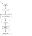
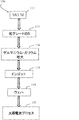
図1は、本開示の背景を表すもので、工程12から始まる公知のプロセス10を示す。工程12において、公知のウェハ形成プロセスフロー10に、MGまたは他の低グレードシリコンが投入される。公知のプロセスフロー10において、工程14でMGシリコンから高グレードシリコンが抽出される。高グレードシリコン抽出工程14は、高コスト処理シーケンスであり、EGシリコン品質か、またはSOG原料品質と呼ばれる若干品質の落ちるシリコン品質が得られる。これらは、工程16においてインゴットを作製するために使用されるタイプのシリコン原材料である。公知のプロセスフロー10は、工程18においてシリコンウェハを得るために、一般に、ワイヤソーを使用してシリコンインゴットをスライスする工程を含んでいる。結果として得られるシリコンウェハは、次に当該ウェハを使用する太陽電池形成プロセス20に投入される。
FIG. 1 represents the background of the present disclosure and shows a known
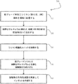
図2は、本願により開示されるプロセスが太陽電池製作フロー30にどのように組み込まれるかについての新規の態様を概括的に示す。本開示によってもたらされるシリコンインゴットの改善された特性は、さまざまなグレードの原材料および本明細書に開示されたゲルマニウム富化工程を使用することによって結果的に得られるウェハの、より向上した機械的強度、および再結合寿命などのより優れた電気的特性を含み得、したがって、結果的に得られる太陽電池の強度および柔軟性が向上することを含み得る。
FIG. 2 generally illustrates a novel aspect of how the process disclosed by the present application is incorporated into the solar
製作フロー30は、工程32においてMGシリコンを使用する工程を含み、MGシリコンは、UMGシリコンになるようにある程度まで精製されてもよい。結果的に得られるシリコン品質は、低グレードシリコン34のままである。したがって、シリコン品質34は、シリコン品質14と比較してはるかに低いコストに関係している。また、低グレードシリコンインゴット34は、シリコン品質14と比較した場合、より高い含有量の金属不純物および非金属不純物を含む。本開示は、結果的に得られるインゴット材料の機械的強度、および電気的特性を高めるために、所定の質および量のゲルマニウム36の添加または増大を含む。シリコンおよびゲルマニウムの組み合わせは、インゴット形成工程38の初期の局面として、シリコン溶融物を形成するために加熱される。
The
工程38において、シリコンインゴット形成は、例えば、方向性凝固プロセス、CZ結晶形成プロセス、またはFZ結晶形成プロセスを用いて行われ得る。実際に適用されるゲルマニウム濃度に基づいて結晶化条件を調節することにより、さらに機械的特性および電気的特性が高められる。工程40は、シリコンウェハの形成を表す。最後に、工程42において太陽電池形成プロセスが行われる。
In
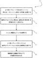
図3は、低グレード未加工シリコン原料を用いた本開示の一つの態様のプロセスフロー50である。プロセスフロー50において、第1の工程52は、低グレード未加工シリコン(例えば、UMGシリコン)を坩堝内に配置することを含む。シリコン溶融物形成用の加熱プロセスを開始する前に、本開示では、工程54において、所定量の純粋なゲルマニウム(例えば、純度99.99パーセントまたは99.999パーセントのゲルマニウム)を低グレードシリコン原料に添加することが企図される。 FIG. 3 is a process flow 50 of one embodiment of the present disclosure using a low grade raw silicon source. In process flow 50, a first step 52 includes placing low grade raw silicon (eg, UMG silicon) in a crucible. Prior to initiating the heating process for forming the silicon melt, the present disclosure includes adding a predetermined amount of pure germanium (eg, 99.99 percent or 99.999 percent purity germanium) to the low grade silicon source in step 54. Intended.
改良されたシリコンに添加されるゲルマニウムの全範囲は、5〜200ppmwの範囲であり得る。別の態様では、5〜50ppmwのゲルマニウムの範囲が可能であり得る。別の態様では、20〜40ppmwのゲルマニウムの範囲が可能であり得る。別の態様では、30〜40ppmwのゲルマニウムの範囲が可能であり得る。別の態様では、50〜100ppmwのゲルマニウムの範囲が可能であり得る。別の態様では、50〜200ppmwのゲルマニウムの範囲が可能であり得る。別の態様では、100〜150ppmwのゲルマニウムの範囲が可能であり得る。別の態様では、120〜180ppmwのゲルマニウムの範囲が可能であり得る。 The total range of germanium added to the modified silicon can range from 5 to 200 ppmw. In another embodiment, a range of 5-50 ppmw germanium may be possible. In another embodiment, a range of 20-40 ppmw germanium may be possible. In another embodiment, a range of 30-40 ppmw germanium may be possible. In another embodiment, a range of 50-100 ppmw germanium may be possible. In another embodiment, a range of 50-200 ppmw germanium may be possible. In another embodiment, a range of 100-150 ppmw germanium may be possible. In another embodiment, a range of 120-180 ppmw germanium may be possible.
固体低グレードシリコンおよび純粋なゲルマニウムの組み合わせが坩堝内に存在すると、次に工程56は、工程58において低グレードシリコンおよび添加ゲルマニウムの溶融物を生成するために固体混合物を加熱することを含む。溶融低グレードシリコンおよびゲルマニウムは、例えば、方向性凝固を実行することによって、その後に工程60において結晶化されてもよい。 Once the combination of solid low grade silicon and pure germanium is present in the crucible, step 56 then includes heating the solid mixture in step 58 to produce a melt of low grade silicon and added germanium. The molten low grade silicon and germanium may be subsequently crystallized in step 60, for example, by performing directional solidification.
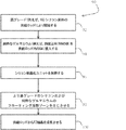
図4は、より高いグレードの未加工シリコン原料を用いた本開示のさらなる態様のプロセスフロー70である。プロセスフロー70において、第1の工程72は、より高いグレードの未加工シリコン(例えば、EGシリコン)を坩堝内に配置することを含む。シリコン溶融物形成用の加熱プロセスを開始する前に、本開示では、工程74において、所定量の純粋なゲルマニウム(例えば、少なくとも純度99.999のゲルマニウム)をより高いグレードのシリコン原料に添加することが企図される。 FIG. 4 is a process flow 70 of a further embodiment of the present disclosure using a higher grade raw silicon source. In process flow 70, a first step 72 includes placing a higher grade of raw silicon (eg, EG silicon) in the crucible. Prior to initiating the heating process for forming the silicon melt, the present disclosure contemplates that in step 74, a predetermined amount of pure germanium (eg, germanium having a purity of at least 99.999) is added to a higher grade silicon source. Is done.
固体低グレードシリコンおよび純粋なゲルマニウムの組み合わせが坩堝内に存在すると、次に工程76は、工程78においてより高いグレードのシリコンおよび添加ゲルマニウムの溶融物を生成するために固体混合物を加熱することを含む。その後、CZプロセスを通して所望の結晶特性を達成および維持するための確立された手法を用いてCZ結晶を引き上げることにより、工程80において、溶融したより高いグレードのシリコンおよびゲルマニウムの一部分を次にシリコン結晶に形成してもよい。 If a combination of solid low grade silicon and pure germanium is present in the crucible, then step 76 includes heating the solid mixture to produce a higher grade silicon and added germanium melt in step 78. . Thereafter, in step 80, a portion of the molten higher grade silicon and germanium is then removed from the silicon crystal by pulling the CZ crystal using established techniques for achieving and maintaining the desired crystal properties throughout the CZ process. You may form in.
図5は、高グレード未加工シリコン、具体的には、EGシリコン原料の供給ロッドから始まる本開示のさらなる態様のプロセスフロー90である。プロセスフロー90において、第1の工程92が、高グレード未加工シリコン(例えば、EGシリコン)供給ロッドから始まる。供給ロッドにより、FZ結晶化プロセスのフローティングゾーンまたはFZ領域を使用できる。FZ領域の形成に関連して、本開示では、工程94において所定量の純粋なゲルマニウム(例えば、少なくとも純度99.999のゲルマニウム)を高グレード未加工シリコン原料の供給ロッドに添加することが企図される。 FIG. 5 is a process flow 90 of a further embodiment of the present disclosure beginning with a supply rod of high grade raw silicon, specifically, EG silicon raw material. In process flow 90, a first step 92 begins with a high grade raw silicon (eg, EG silicon) supply rod. Depending on the supply rod, the floating zone or FZ region of the FZ crystallization process can be used. In connection with the formation of the FZ region, the present disclosure contemplates adding a predetermined amount of pure germanium (eg, germanium with a purity of at least 99.999) to a high grade raw silicon source feed rod in step 94.
固体高グレードシリコンおよび純ゲルマニウムの組み合わせがFZに存在すると、次に工程96は、工程98において、より高いグレードのシリコンおよび添加ゲルマニウムのフローティング溶融ゾーンを使用し、工程100において、供給ロッドおよびゲルマニウムの混合物からFZ結晶を成長させることによって次にシリコン結晶を形成する。この点において、FZプロセスを通して所望の結晶特性を達成および維持するための定型手法が適用されうる。 If a combination of solid high grade silicon and pure germanium is present in the FZ, then step 96 uses a higher grade silicon and additive germanium floating melting zone in step 98 and in step 100 the feed rod and germanium Silicon crystals are then formed by growing FZ crystals from the mixture. In this regard, routine techniques for achieving and maintaining desired crystal properties through the FZ process can be applied.
図6は、太陽電池製作フロー130全体に統合することができる別のプロセスの新規の側面を概括的に表している。製作フロー130は、工程132においてMGシリコンを使用する工程を含み、当該MGシリコンは、UMGシリコンとなるようにある程度精製されてもよい。結果として得られるシリコンの品質は、依然として、低グレードシリコン134を生じる。したがって、シリコン品質134は、図1において説明されるような改質されていないシリコンと比較してはるかに低いコストに関係している。さらに、低グレードシリコンインゴット134は、改質されていないシリコンと比較して、より高い含有量の金属不純物および非金属不純物を含む。本開示は、結果として得られるインゴットの機械的特性および電気的特性を含む特性のさらなる向上のために、ガリウム136の所定の品質および量のさらなる追加または増大と併せて、ゲルマニウムの添加を含む。一例において、ガリウムは、0〜10ppmwの範囲の濃度で添加される。シリコンとゲルマニウムおよびガリウムとの組み合わせは、インゴット形成工程138の初期の局面として、シリコン溶融物を形成するために加熱される。
FIG. 6 generally represents a novel aspect of another process that can be integrated into the overall solar
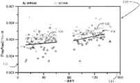
図7は、インゴットBからのゲルマニウムドーピングされた一例の材料の機械的ウェハ強度を、インゴットAからのドーピングされていない参照材料と比較した実験の特徴的な結果110を示す。両方のインゴットについて、極めて同じタイプのUMG原料シリコンを選択し、同じ鋳造条件を適用し同じツールを用いて、連続して鋳造を行った。次に、各インゴットから、1セットの底部付近のウェハ(116および120)および1セットの上部付近のウェハ(118および122)を選択し、標準的な4直線曲げ試験(4-line bending test)において最大外力Fmaxと最大ウェハ変形lmaxの比率として測定された、機械的ウェハ強度を求めた。正規化されたウェハ強度(強度をウェハの厚さで除算)112は、一連番号114がそれぞれのインゴット内の元の場所を表す(番号が大きくなるほど、底部から上部へ)さまざまなウェハ群に対して与えられる。グラフから、ゲルマニウムドーピングされたインゴットBからのウェハが、参照インゴットAからのウェハより強度が高いことが分かった。ここに示す結果は、シリコンインゴットを形成する際にゲルマニウムを添加すると、他の方法で同様に形成されたシリコンインゴットからなるシリコンインゴットよりも強度特性が優れるという結論を支持する。
FIG. 7 shows a
これらの結果は、ゲルマニウムドーピングされたシリコンインゴット由来の材料を用いることで達成されるその他の改良例を示している以下の表によって、さらに実証される。 These results are further demonstrated by the following table showing other improvements achieved using materials derived from germanium doped silicon ingots.
(表)インゴットの歩留まり、キャリア寿命、および効率の向上
表は、多結晶シリコンインゴットの形成に使用した中間グレード原料に関するデータについて報告したものである。上記のデータは、上述した改善された機械的特性に加えて、電気的材料特性の改善を示す。同表における電気的特性の改善値は、本開示による改良がなされていないシリコンと比較した、上記の態様において説明される増強されたシリコンにおける向上をパーセンテージとして示している。材料特性が改善されるため、このようなインゴットからのシリコンウェハ数および関連する太陽電池数におけるそれぞれの歩留まりが向上する。さらに、電気的特性が改善されることにより、結果的に得られる太陽電池の平均の歩留まりが向上する。 The table reports data on intermediate grade raw materials used to form polycrystalline silicon ingots. The above data shows an improvement in electrical material properties in addition to the improved mechanical properties described above. The electrical property improvement values in the table show the improvement in the enhanced silicon described in the above embodiment as a percentage compared to silicon that has not been improved according to the present disclosure. Because the material properties are improved, the respective yields in the number of silicon wafers and associated solar cells from such ingots are improved. Furthermore, by improving the electrical characteristics, the average yield of the resulting solar cells is improved.
言い換えれば、本開示の教示によって、形成されるシリコンインゴットの材料特性が改善され、カスケード効果によって、太陽電池およびこのような太陽電池を使用したシステムの製造に関連する最終的なコストの削減が促される。すなわち、ゲルマニウムドーピングされたシリコン材料は、非ドーピングシリコン材料より優れた材料強度および柔軟性を備えるため、インゴットからウェハをスライスする機械的プロセスの際のウェハ破損が低減する可能性が高くなる。次に、ウェハがスライスされた後も、シリコンウェハの材料強度および柔軟性は持続し、このようなシリコンウェハがさらに太陽電池に形成されるため、太陽電池の耐久性が増す。さらに、このようにして結果的に得られる太陽電池は、太陽電池製造場所から太陽電池アレイとしての組み立て場所やこのような太陽電池アレイの分野における最終的な設置場所までの輸送時または設置時に、破損、亀裂、または破砕応力が生じにくくなる。最後に、現場での風化作用、熱的および環境的過渡現象が太陽電池に損傷を与えたり、そのほかの現象を引き起こしたりするため、このような太陽電池の耐久性や柔軟性が向上することで、太陽電池アレイの動作寿命がさらに向上し得る。 In other words, the teachings of the present disclosure improve the material properties of the formed silicon ingot, and the cascading effect encourages a reduction in the final costs associated with manufacturing solar cells and systems using such solar cells. It is. That is, the germanium doped silicon material has better material strength and flexibility than the undoped silicon material, thus increasing the possibility of reducing wafer breakage during the mechanical process of slicing the wafer from the ingot. Next, even after the wafer is sliced, the material strength and flexibility of the silicon wafer will persist and such a silicon wafer will be further formed into the solar cell, increasing the durability of the solar cell. Further, the resulting solar cell is thus transported or installed from the solar cell manufacturing site to the assembly site as a solar cell array or the final installation site in the field of such solar cell array, Damage, cracking, or crushing stress is less likely to occur. Finally, on-site weathering, thermal and environmental transients can damage solar cells and cause other phenomena, increasing the durability and flexibility of these solar cells. The operating life of the solar cell array can be further improved.
本開示の教示の実施によるシリコンウェハの歩留まりの向上、太陽電池の歩留まりの向上、太陽電池アレイの歩留まりの向上、および太陽電池アレイの機械的耐久性の向上により、太陽電池産業において著しく高い経済性が生じ得る。このような経済性により、太陽電池の発電コストが直接的および実質的に削減される。 Remarkably high economics in the solar cell industry due to improved silicon wafer yield, improved solar cell yield, improved solar cell array yield, and improved solar cell mechanical durability by implementing the teachings of the present disclosure Can occur. Such economy directly and substantially reduces the power generation cost of the solar cell.
上記の表が示すように、ゲルマニウムドーピングの例は、シリコン材料のそれぞれのキャリア寿命が向上するだけでなく、太陽電池全体の効率も向上する。例えば、上記の表において、20.7%の再結合寿命の向上が示され、1.2%の電池効率の向上が測定されていることが示されている。 As the above table shows, the germanium doping example not only improves the respective carrier lifetime of the silicon material, but also improves the overall efficiency of the solar cell. For example, the table above shows a 20.7% increase in recombination lifetime and a 1.2% increase in battery efficiency measured.
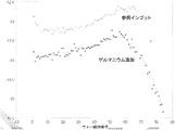
図8はさらに、本開示において説明されるような、ゲルマニウム添加の結果としての、シリコン材料の電気的特性におけるさらなる改良を示している。図は、ウェハ識別番号に対する破壊電圧を示しており、小さいウェハ識別番号ほど、インゴットの底部に近い位置を示しており、大きいウェハ識別番号ほど、インゴットの上部に近い位置を示している。図から分かるように、参照インゴットデータ150は、本発明の態様に従って処理されたインゴット152よりも、一貫して低い破壊電圧を示している。 FIG. 8 further shows further improvements in the electrical properties of the silicon material as a result of germanium addition, as described in this disclosure. The figure shows the breakdown voltage with respect to the wafer identification number. The smaller the wafer identification number, the closer to the bottom of the ingot, and the larger the wafer identification number, the closer to the top of the ingot. As can be seen, the reference ingot data 150 shows a consistently lower breakdown voltage than the ingot 152 processed in accordance with aspects of the present invention.
一例において、シリコンに添加するゲルマニウムの有効量の選択は、いくつかの潜在的に競合する因子に応じて変わる。例えば、強度および柔軟性などの機械的特性は、より多くのゲルマニウムを添加することによって増強されるが、ある濃度を超えて添加すると、シリコンカーバイドの形成など、望ましくない効果を生じ得る。したがって、例えば、5〜50ppmwの範囲のゲルマニウムの濃度は、望ましくない効果を最小限に維持しつつ、増強された機械的強度および低い転位密度と共に、増強された電気的特性、例えば、低い光劣化および長い再結合寿命など、を提供する。一例において、ゲルマニウムの有効量は、0〜20ppmwの範囲のゲルマニウム濃度を含む。一例において、ゲルマニウムの有効量は、30〜60ppmwの範囲のゲルマニウム濃度を含む。 In one example, the selection of an effective amount of germanium to add to silicon varies depending on a number of potentially competing factors. For example, mechanical properties such as strength and flexibility are enhanced by adding more germanium, but adding above a certain concentration can produce undesirable effects such as the formation of silicon carbide. Thus, for example, germanium concentrations in the range of 5-50 ppmw have enhanced electrical properties, such as low photodegradation, with enhanced mechanical strength and low dislocation density, while keeping undesirable effects to a minimum. And provide a long recombination lifetime, etc. In one example, an effective amount of germanium includes a germanium concentration in the range of 0-20 ppmw. In one example, an effective amount of germanium includes a germanium concentration in the range of 30-60 ppmw.
本開示のシリコン材料の改善は、結晶シリコンの格子構造に置換的にゲルマニウム原子が取り込まれることに関連して、圧縮格子歪みが増大することから得られ得る。このようなゲルマニウムの置換的取り込みは、シリコンウェハまたは太陽電池のある特定のバルク欠陥に付随する局所的な引っ張り応力を相殺し、本来の材料強度の制御の向上をもたらす。 Improvements in the silicon material of the present disclosure can be obtained from the increased compressive lattice distortion associated with the incorporation of germanium atoms in the lattice structure of crystalline silicon. Such substitutional incorporation of germanium counteracts local tensile stress associated with certain bulk defects in silicon wafers or solar cells, resulting in improved control of the inherent material strength.
経験的な結果によれば、十分量のゲルマニウムを含むシリコン材料は、材料強度の向上を示す。最良の実用範囲は、生成された材料の品質に依存する。ゲルマニウム濃度がわずかに高いと、単結晶シリコンは多結晶シリコンより良好に機能することが分かった。 Empirical results show that silicon materials containing a sufficient amount of germanium show improved material strength. The best practical range depends on the quality of the material produced. It was found that single crystal silicon performs better than polycrystalline silicon at a slightly higher germanium concentration.
要約すると、開示された主題により、シリコン原料および所定量のゲルマニウムから溶融液を坩堝デバイス内で形成する工程の後、坩堝内でインゴットを形成するための方向性凝固、溶融物からのCZ結晶の引き上げ、またはFZ結晶の成長のいずれかが行われるシリコンインゴットまたは結晶の形成方法およびシステムが提供される。 In summary, according to the disclosed subject matter, after forming a melt in a crucible device from a silicon raw material and a predetermined amount of germanium, directional solidification to form an ingot in the crucible, the CZ crystal from the melt Methods and systems for forming silicon ingots or crystals that are either pulled up or grown in FZ crystals are provided.
本明細書において、本開示の教示を取り入れたさまざまな態様を詳細に示し記載してきたが、当業者によれば、これらの教示を取り入れた多くの他の変更された態様を容易に考案できるであろう。したがって、好ましい態様の前述した記載は、当業者が、主張された主題を製造または使用することができるように提供される。これらの態様のさまざまな修正は、当業者に容易に明らかであり、本明細書において規定された一般的な原理は、革新的な能力を用いなくても他の態様に応用され得る。このように、主張された主題は、本明細書に示す態様に限定されることを意図したものではなく、本明細書において開示された原理および新規の特徴と一致する最も広い範囲に従うものとする。 While various aspects incorporating the teachings of this disclosure have been shown and described herein in detail, those skilled in the art can readily devise many other modified aspects incorporating these teachings. I will. Accordingly, the foregoing description of preferred embodiments is provided to enable any person skilled in the art to make or use the claimed subject matter. Various modifications of these aspects will be readily apparent to those skilled in the art, and the general principles defined herein may be applied to other aspects without the use of innovative capabilities. Thus, the claimed subject matter is not intended to be limited to the embodiments shown herein but is to be accorded the widest scope consistent with the principles and novel features disclosed herein. .
Claims (12)
該シリコン原材料に、5〜50ppmwの範囲である所定量のゲルマニウムを添加する工程;
シリコン原材料および該量のゲルマニウムのそれぞれから溶融物を生成する工程;および
該溶融物の結晶化を実施する工程
を含む、改良された機械的特性および電気的特性を有する結晶シリコンを形成するための方法。 Initiating a silicon crystallization process using a predetermined amount of silicon raw material;
Adding a predetermined amount of germanium in the range of 5 to 50 ppmw to the silicon raw material;
Forming crystalline silicon having improved mechanical and electrical properties, comprising: generating a melt from each of the silicon raw material and the amount of germanium; and performing crystallization of the melt Method.
Applications Claiming Priority (3)
| Application Number | Priority Date | Filing Date | Title |
|---|---|---|---|
| US12/954,498 | 2010-11-24 | ||
| US12/954,498 US8758507B2 (en) | 2008-06-16 | 2010-11-24 | Germanium enriched silicon material for making solar cells |
| PCT/US2011/062075 WO2012071531A1 (en) | 2010-11-24 | 2011-11-23 | Germanium enriched silicon for solar cells |
Publications (2)
| Publication Number | Publication Date |
|---|---|
| JP2013545706A true JP2013545706A (en) | 2013-12-26 |
| JP2013545706A5 JP2013545706A5 (en) | 2015-01-15 |
Family
ID=45316074
Family Applications (1)
| Application Number | Title | Priority Date | Filing Date |
|---|---|---|---|
| JP2013541051A Pending JP2013545706A (en) | 2010-11-24 | 2011-11-23 | Germanium-enriched silicon for solar cells |
Country Status (8)
| Country | Link |
|---|---|
| US (2) | US8758507B2 (en) |
| EP (1) | EP2643500A1 (en) |
| JP (1) | JP2013545706A (en) |
| KR (1) | KR20130115296A (en) |
| CN (1) | CN103237928A (en) |
| BR (1) | BR112013012484A2 (en) |
| TW (1) | TW201226638A (en) |
| WO (1) | WO2012071531A1 (en) |
Families Citing this family (3)
| Publication number | Priority date | Publication date | Assignee | Title |
|---|---|---|---|---|
| US8758507B2 (en) * | 2008-06-16 | 2014-06-24 | Silicor Materials Inc. | Germanium enriched silicon material for making solar cells |
| WO2013132629A1 (en) * | 2012-03-08 | 2013-09-12 | 新日鉄マテリアルズ株式会社 | Method for manufacturing highly pure silicon, highly pure silicon obtained by this method, and silicon raw material for manufacturing highly pure silicon |
| CN105019022A (en) * | 2015-08-12 | 2015-11-04 | 常州天合光能有限公司 | Quasi mono-crystalline silicon co-doped with gallium, germanium and boron and preparing method thereof |
Citations (4)
| Publication number | Priority date | Publication date | Assignee | Title |
|---|---|---|---|---|
| JPS59121193A (en) * | 1982-12-27 | 1984-07-13 | Fujitsu Ltd | Silicon crystal |
| CN101597794A (en) * | 2009-06-24 | 2009-12-09 | 浙江大学 | The czochralski silicon monocrystal that a kind of gallium and germanium are mixed altogether |
| WO2010005736A2 (en) * | 2008-06-16 | 2010-01-14 | Calisolar, Inc. | Germanium-enriched silicon material for making solar cells |
| JP2010215455A (en) * | 2009-03-17 | 2010-09-30 | Tohoku Univ | Si CRYSTAL AND METHOD FOR MANUFACTURING THE SAME |
Family Cites Families (33)
| Publication number | Priority date | Publication date | Assignee | Title |
|---|---|---|---|---|
| CA1147698A (en) * | 1980-10-15 | 1983-06-07 | Maher I. Boulos | Purification of metallurgical grade silicon |
| US4392297A (en) | 1980-11-20 | 1983-07-12 | Spire Corporation | Process of making thin film high efficiency solar cells |
| US5069740A (en) | 1984-09-04 | 1991-12-03 | Texas Instruments Incorporated | Production of semiconductor grade silicon spheres from metallurgical grade silicon particles |
| US4631234A (en) * | 1985-09-13 | 1986-12-23 | Texas Instruments Incorporated | Germanium hardened silicon substrate |
| US4910153A (en) * | 1986-02-18 | 1990-03-20 | Solarex Corporation | Deposition feedstock and dopant materials useful in the fabrication of hydrogenated amorphous silicon alloys for photovoltaic devices and other semiconductor devices |
| JPH03270210A (en) | 1990-03-20 | 1991-12-02 | Fujitsu Ltd | Silicon wafer |
| JP2695585B2 (en) * | 1992-12-28 | 1997-12-24 | キヤノン株式会社 | Photovoltaic element, method of manufacturing the same, and power generator using the same |
| JPH06326024A (en) | 1993-05-10 | 1994-11-25 | Canon Inc | Manufacture of semiconductor substrate, and method of depositing amorphous film |
| US5556791A (en) * | 1995-01-03 | 1996-09-17 | Texas Instruments Incorporated | Method of making optically fused semiconductor powder for solar cells |
| US5553566A (en) * | 1995-06-22 | 1996-09-10 | Motorola Inc. | Method of eliminating dislocations and lowering lattice strain for highly doped N+ substrates |
| JP3531333B2 (en) * | 1996-02-14 | 2004-05-31 | 信越半導体株式会社 | Crystal manufacturing apparatus by Czochralski method, crystal manufacturing method, and crystal manufactured by this method |
| US5730808A (en) * | 1996-06-27 | 1998-03-24 | Amoco/Enron Solar | Producing solar cells by surface preparation for accelerated nucleation of microcrystalline silicon on heterogeneous substrates |
| EP0888398A4 (en) * | 1996-12-16 | 1999-09-29 | Corning Inc | Germanium doped silica forming feedstock and method |
| NO333319B1 (en) * | 2003-12-29 | 2013-05-06 | Elkem As | Silicon material for the production of solar cells |
| US8129822B2 (en) * | 2006-10-09 | 2012-03-06 | Solexel, Inc. | Template for three-dimensional thin-film solar cell manufacturing and methods of use |
| US20090107545A1 (en) * | 2006-10-09 | 2009-04-30 | Soltaix, Inc. | Template for pyramidal three-dimensional thin-film solar cell manufacturing and methods of use |
| NO322246B1 (en) * | 2004-12-27 | 2006-09-04 | Elkem Solar As | Process for preparing directed solidified silicon ingots |
| JP2007019209A (en) * | 2005-07-07 | 2007-01-25 | Sumco Solar Corp | Polycrystalline silicone for solar cell and its manufacturing method |
| US8017862B2 (en) * | 2005-10-21 | 2011-09-13 | Sumco Solar Corporation | Solar-cell single-crystal silicon substrate, solar cell element, and method for producing the same |
| JP2007142370A (en) | 2005-10-21 | 2007-06-07 | Sumco Solar Corp | Silicon monocrystalline substrate for solar cell, solar cell element, and manufacturing method therefor |
| JP2007137756A (en) | 2005-10-21 | 2007-06-07 | Sumco Solar Corp | Solar cell silicon single crystal substrate, solar cell element, and method for producing the same |
| EP1974076A2 (en) * | 2006-01-20 | 2008-10-01 | BP Corporation North America Inc. | Methods and apparatuses for manufacturing geometric multicrystalline cast silicon and geometric multicrystalline cast silicon bodies for photovoltaics |
| US7928317B2 (en) | 2006-06-05 | 2011-04-19 | Translucent, Inc. | Thin film solar cell |
| US20080264477A1 (en) * | 2006-10-09 | 2008-10-30 | Soltaix, Inc. | Methods for manufacturing three-dimensional thin-film solar cells |
| JP2008157343A (en) | 2006-12-22 | 2008-07-10 | Pascal Engineering Corp | Gas spring |
| US8008107B2 (en) * | 2006-12-30 | 2011-08-30 | Calisolar, Inc. | Semiconductor wafer pre-process annealing and gettering method and system for solar cell formation |
| US20080197454A1 (en) * | 2007-02-16 | 2008-08-21 | Calisolar, Inc. | Method and system for removing impurities from low-grade crystalline silicon wafers |
| TW200914371A (en) * | 2007-06-01 | 2009-04-01 | Gt Solar Inc | Processing of fine silicon powder to produce bulk silicon |
| US8071872B2 (en) * | 2007-06-15 | 2011-12-06 | Translucent Inc. | Thin film semi-conductor-on-glass solar cell devices |
| US20080314446A1 (en) * | 2007-06-25 | 2008-12-25 | General Electric Company | Processes for the preparation of solar-grade silicon and photovoltaic cells |
| US20080314445A1 (en) * | 2007-06-25 | 2008-12-25 | General Electric Company | Method for the preparation of high purity silicon |
| US8758507B2 (en) | 2008-06-16 | 2014-06-24 | Silicor Materials Inc. | Germanium enriched silicon material for making solar cells |
| CN101591808A (en) | 2009-06-24 | 2009-12-02 | 浙江大学 | Mix directionally solidified casting monocrystalline silicon of germanium and preparation method thereof |
-
2010
- 2010-11-24 US US12/954,498 patent/US8758507B2/en not_active Expired - Fee Related
-
2011
- 2011-11-23 BR BR112013012484A patent/BR112013012484A2/en not_active IP Right Cessation
- 2011-11-23 KR KR1020137015219A patent/KR20130115296A/en not_active Application Discontinuation
- 2011-11-23 TW TW100142927A patent/TW201226638A/en unknown
- 2011-11-23 JP JP2013541051A patent/JP2013545706A/en active Pending
- 2011-11-23 WO PCT/US2011/062075 patent/WO2012071531A1/en active Application Filing
- 2011-11-23 EP EP11794306.8A patent/EP2643500A1/en not_active Withdrawn
- 2011-11-23 CN CN2011800564795A patent/CN103237928A/en active Pending
-
2014
- 2014-06-23 US US14/312,026 patent/US20150020729A1/en not_active Abandoned
Patent Citations (4)
| Publication number | Priority date | Publication date | Assignee | Title |
|---|---|---|---|---|
| JPS59121193A (en) * | 1982-12-27 | 1984-07-13 | Fujitsu Ltd | Silicon crystal |
| WO2010005736A2 (en) * | 2008-06-16 | 2010-01-14 | Calisolar, Inc. | Germanium-enriched silicon material for making solar cells |
| JP2010215455A (en) * | 2009-03-17 | 2010-09-30 | Tohoku Univ | Si CRYSTAL AND METHOD FOR MANUFACTURING THE SAME |
| CN101597794A (en) * | 2009-06-24 | 2009-12-09 | 浙江大学 | The czochralski silicon monocrystal that a kind of gallium and germanium are mixed altogether |
Non-Patent Citations (1)
| Title |
|---|
| JPN6015021719; Mukannan Arivanandhan: 'High minority carrier lifetime in Ga-doped Czochralski-grown silicon by Ge codoping' APPLIED PHYSICS LETTERS 94,072102(2009), 2009 * |
Also Published As
| Publication number | Publication date |
|---|---|
| TW201226638A (en) | 2012-07-01 |
| US20150020729A1 (en) | 2015-01-22 |
| BR112013012484A2 (en) | 2016-09-06 |
| KR20130115296A (en) | 2013-10-21 |
| WO2012071531A1 (en) | 2012-05-31 |
| US8758507B2 (en) | 2014-06-24 |
| US20110126758A1 (en) | 2011-06-02 |
| CN103237928A (en) | 2013-08-07 |
| EP2643500A1 (en) | 2013-10-02 |
Similar Documents
| Publication | Publication Date | Title |
|---|---|---|
| JP5661033B2 (en) | Germanium-enriched silicon material for solar cell manufacturing | |
| EP2173660B1 (en) | Method for controlling resistivity in ingots made of compensated feedstock silicon | |
| US7381392B2 (en) | Silicon feedstock for solar cells | |
| US20110030793A1 (en) | Method for producing photovoltaic-grade crystalline silicon by addition of doping impurities and photovoltaic cell | |
| JP2008525297A (en) | Method for producing directional solidified silicon ingot | |
| US20140127496A1 (en) | Crystalline silicon ingot including nucleation promotion layer and method of fabricating the same | |
| Ganesh et al. | Growth and characterization of multicrystalline silicon ingots by directional solidification for solar cell applications | |
| JP2013545706A (en) | Germanium-enriched silicon for solar cells | |
| Huang et al. | Growth and Defects in Cast‐Mono Silicon for Solar Cells: A Review | |
| JP2007194513A (en) | Manufacturing method for crystal semiconductor particle, and photovoltaic conversion device | |
| Verlinden | Doping, diffusion, and defects in solar cells | |
| Degoulange et al. | Dopant specifications for p-type UMG silicon: mono-c vs multi-c | |
| TWI600808B (en) | Method of manufacturing polycrystalline silicon ingot, method of making polycrystalline silicon ingot, and polycrystalline silicon ingot | |
| Arnberg et al. | Solidification of silicon for solar cells | |
| CN117364223A (en) | Preparation method of cast monocrystalline silicon ingot for inhibiting dislocation movement proliferation | |
| US10483428B2 (en) | Multicrystalline silicon ingots, silicon masteralloy, method for increasing the yield of multicrystalline silicon ingots for solar cells | |
| CN110550634A (en) | Polycrystalline silicon rod |
Legal Events
| Date | Code | Title | Description |
|---|---|---|---|
| A521 | Written amendment |
Free format text: JAPANESE INTERMEDIATE CODE: A523 Effective date: 20141112 |
|
| A621 | Written request for application examination |
Free format text: JAPANESE INTERMEDIATE CODE: A621 Effective date: 20141112 |
|
| RD04 | Notification of resignation of power of attorney |
Free format text: JAPANESE INTERMEDIATE CODE: A7424 Effective date: 20150514 |
|
| A977 | Report on retrieval |
Free format text: JAPANESE INTERMEDIATE CODE: A971007 Effective date: 20150529 |
|
| A131 | Notification of reasons for refusal |
Free format text: JAPANESE INTERMEDIATE CODE: A131 Effective date: 20150603 |
|
| A601 | Written request for extension of time |
Free format text: JAPANESE INTERMEDIATE CODE: A601 Effective date: 20150826 |
|
| A02 | Decision of refusal |
Free format text: JAPANESE INTERMEDIATE CODE: A02 Effective date: 20160404 |