JP2013534319A - Position measuring device - Google Patents
Position measuring device Download PDFInfo
- Publication number
- JP2013534319A JP2013534319A JP2013524324A JP2013524324A JP2013534319A JP 2013534319 A JP2013534319 A JP 2013534319A JP 2013524324 A JP2013524324 A JP 2013524324A JP 2013524324 A JP2013524324 A JP 2013524324A JP 2013534319 A JP2013534319 A JP 2013534319A
- Authority
- JP
- Japan
- Prior art keywords
- housing
- sensor head
- optical receiver
- rotary encoder
- sensor
- Prior art date
- Legal status (The legal status is an assumption and is not a legal conclusion. Google has not performed a legal analysis and makes no representation as to the accuracy of the status listed.)
- Pending
Links
- 230000003287 optical effect Effects 0.000 claims abstract description 188
- 238000005259 measurement Methods 0.000 claims description 4
- 239000010410 layer Substances 0.000 description 96
- 239000000758 substrate Substances 0.000 description 92
- 238000000034 method Methods 0.000 description 40
- 238000013461 design Methods 0.000 description 25
- 239000011521 glass Substances 0.000 description 21
- 239000000853 adhesive Substances 0.000 description 18
- 230000001070 adhesive effect Effects 0.000 description 18
- 230000008569 process Effects 0.000 description 18
- 238000004519 manufacturing process Methods 0.000 description 17
- 230000006870 function Effects 0.000 description 15
- 239000004020 conductor Substances 0.000 description 13
- 238000005530 etching Methods 0.000 description 13
- 229910052751 metal Inorganic materials 0.000 description 13
- 239000002184 metal Substances 0.000 description 13
- 230000008901 benefit Effects 0.000 description 12
- 239000004065 semiconductor Substances 0.000 description 12
- 239000010409 thin film Substances 0.000 description 12
- 229910052782 aluminium Inorganic materials 0.000 description 11
- XAGFODPZIPBFFR-UHFFFAOYSA-N aluminium Chemical compound [Al] XAGFODPZIPBFFR-UHFFFAOYSA-N 0.000 description 11
- 238000006243 chemical reaction Methods 0.000 description 11
- 239000000463 material Substances 0.000 description 11
- 239000012876 carrier material Substances 0.000 description 10
- 239000004033 plastic Substances 0.000 description 8
- 229920003023 plastic Polymers 0.000 description 8
- 229910021417 amorphous silicon Inorganic materials 0.000 description 7
- PCHJSUWPFVWCPO-UHFFFAOYSA-N gold Chemical compound [Au] PCHJSUWPFVWCPO-UHFFFAOYSA-N 0.000 description 7
- 229910052737 gold Inorganic materials 0.000 description 7
- 239000010931 gold Substances 0.000 description 7
- 230000005484 gravity Effects 0.000 description 7
- 230000000875 corresponding effect Effects 0.000 description 6
- 125000006850 spacer group Chemical group 0.000 description 6
- 229910000679 solder Inorganic materials 0.000 description 5
- 229910004298 SiO 2 Inorganic materials 0.000 description 4
- 238000010586 diagram Methods 0.000 description 4
- 238000009826 distribution Methods 0.000 description 4
- 238000012545 processing Methods 0.000 description 4
- 239000004809 Teflon Substances 0.000 description 3
- 229920006362 Teflon® Polymers 0.000 description 3
- 230000015572 biosynthetic process Effects 0.000 description 3
- 239000000919 ceramic Substances 0.000 description 3
- 230000008859 change Effects 0.000 description 3
- 238000000576 coating method Methods 0.000 description 3
- 238000005516 engineering process Methods 0.000 description 3
- 239000010408 film Substances 0.000 description 3
- 238000000227 grinding Methods 0.000 description 3
- 238000009434 installation Methods 0.000 description 3
- 238000010884 ion-beam technique Methods 0.000 description 3
- 238000005192 partition Methods 0.000 description 3
- 238000000623 plasma-assisted chemical vapour deposition Methods 0.000 description 3
- 239000011241 protective layer Substances 0.000 description 3
- 230000007704 transition Effects 0.000 description 3
- PXHVJJICTQNCMI-UHFFFAOYSA-N Nickel Chemical compound [Ni] PXHVJJICTQNCMI-UHFFFAOYSA-N 0.000 description 2
- BLRPTPMANUNPDV-UHFFFAOYSA-N Silane Chemical group [SiH4] BLRPTPMANUNPDV-UHFFFAOYSA-N 0.000 description 2
- 230000002411 adverse Effects 0.000 description 2
- 230000005540 biological transmission Effects 0.000 description 2
- 229910052796 boron Inorganic materials 0.000 description 2
- 238000005229 chemical vapour deposition Methods 0.000 description 2
- 239000011248 coating agent Substances 0.000 description 2
- 238000010276 construction Methods 0.000 description 2
- 238000011156 evaluation Methods 0.000 description 2
- 238000002161 passivation Methods 0.000 description 2
- 229920002120 photoresistant polymer Polymers 0.000 description 2
- 239000002985 plastic film Substances 0.000 description 2
- 229920006255 plastic film Polymers 0.000 description 2
- 229920001721 polyimide Polymers 0.000 description 2
- 230000000630 rising effect Effects 0.000 description 2
- 229910000077 silane Inorganic materials 0.000 description 2
- 238000013519 translation Methods 0.000 description 2
- 238000007740 vapor deposition Methods 0.000 description 2
- ZOXJGFHDIHLPTG-UHFFFAOYSA-N Boron Chemical compound [B] ZOXJGFHDIHLPTG-UHFFFAOYSA-N 0.000 description 1
- 239000004593 Epoxy Substances 0.000 description 1
- 239000004642 Polyimide Substances 0.000 description 1
- RTAQQCXQSZGOHL-UHFFFAOYSA-N Titanium Chemical compound [Ti] RTAQQCXQSZGOHL-UHFFFAOYSA-N 0.000 description 1
- 229910045601 alloy Inorganic materials 0.000 description 1
- 239000000956 alloy Substances 0.000 description 1
- 239000012141 concentrate Substances 0.000 description 1
- 238000012937 correction Methods 0.000 description 1
- 230000002596 correlated effect Effects 0.000 description 1
- 238000005336 cracking Methods 0.000 description 1
- 238000005520 cutting process Methods 0.000 description 1
- 238000009792 diffusion process Methods 0.000 description 1
- 238000006073 displacement reaction Methods 0.000 description 1
- 230000000694 effects Effects 0.000 description 1
- 238000011049 filling Methods 0.000 description 1
- 239000012467 final product Substances 0.000 description 1
- 239000007789 gas Substances 0.000 description 1
- 230000007274 generation of a signal involved in cell-cell signaling Effects 0.000 description 1
- 229910052732 germanium Inorganic materials 0.000 description 1
- GNPVGFCGXDBREM-UHFFFAOYSA-N germanium atom Chemical compound [Ge] GNPVGFCGXDBREM-UHFFFAOYSA-N 0.000 description 1
- 230000001771 impaired effect Effects 0.000 description 1
- 238000007689 inspection Methods 0.000 description 1
- 230000010354 integration Effects 0.000 description 1
- 230000007794 irritation Effects 0.000 description 1
- 239000000203 mixture Substances 0.000 description 1
- 238000012986 modification Methods 0.000 description 1
- 230000004048 modification Effects 0.000 description 1
- 229910052759 nickel Inorganic materials 0.000 description 1
- 239000012811 non-conductive material Substances 0.000 description 1
- 230000003647 oxidation Effects 0.000 description 1
- 238000007254 oxidation reaction Methods 0.000 description 1
- 238000003825 pressing Methods 0.000 description 1
- 239000000047 product Substances 0.000 description 1
- 230000006798 recombination Effects 0.000 description 1
- 238000005215 recombination Methods 0.000 description 1
- 230000002441 reversible effect Effects 0.000 description 1
- 238000007789 sealing Methods 0.000 description 1
- 230000009131 signaling function Effects 0.000 description 1
- 239000007858 starting material Substances 0.000 description 1
- 238000003860 storage Methods 0.000 description 1
- 229920003002 synthetic resin Polymers 0.000 description 1
- 239000000057 synthetic resin Substances 0.000 description 1
- 239000010936 titanium Substances 0.000 description 1
- 229910052719 titanium Inorganic materials 0.000 description 1
- 238000011179 visual inspection Methods 0.000 description 1
- 238000003466 welding Methods 0.000 description 1
Images


Classifications
-
- G—PHYSICS
- G01—MEASURING; TESTING
- G01B—MEASURING LENGTH, THICKNESS OR SIMILAR LINEAR DIMENSIONS; MEASURING ANGLES; MEASURING AREAS; MEASURING IRREGULARITIES OF SURFACES OR CONTOURS
- G01B11/00—Measuring arrangements characterised by the use of optical techniques
- G01B11/14—Measuring arrangements characterised by the use of optical techniques for measuring distance or clearance between spaced objects or spaced apertures
-
- B—PERFORMING OPERATIONS; TRANSPORTING
- B23—MACHINE TOOLS; METAL-WORKING NOT OTHERWISE PROVIDED FOR
- B23Q—DETAILS, COMPONENTS, OR ACCESSORIES FOR MACHINE TOOLS, e.g. ARRANGEMENTS FOR COPYING OR CONTROLLING; MACHINE TOOLS IN GENERAL CHARACTERISED BY THE CONSTRUCTION OF PARTICULAR DETAILS OR COMPONENTS; COMBINATIONS OR ASSOCIATIONS OF METAL-WORKING MACHINES, NOT DIRECTED TO A PARTICULAR RESULT
- B23Q7/00—Arrangements for handling work specially combined with or arranged in, or specially adapted for use in connection with, machine tools, e.g. for conveying, loading, positioning, discharging, sorting
- B23Q7/06—Arrangements for handling work specially combined with or arranged in, or specially adapted for use in connection with, machine tools, e.g. for conveying, loading, positioning, discharging, sorting by means of pushers
-
- G—PHYSICS
- G01—MEASURING; TESTING
- G01B—MEASURING LENGTH, THICKNESS OR SIMILAR LINEAR DIMENSIONS; MEASURING ANGLES; MEASURING AREAS; MEASURING IRREGULARITIES OF SURFACES OR CONTOURS
- G01B11/00—Measuring arrangements characterised by the use of optical techniques
-
- G—PHYSICS
- G01—MEASURING; TESTING
- G01D—MEASURING NOT SPECIALLY ADAPTED FOR A SPECIFIC VARIABLE; ARRANGEMENTS FOR MEASURING TWO OR MORE VARIABLES NOT COVERED IN A SINGLE OTHER SUBCLASS; TARIFF METERING APPARATUS; MEASURING OR TESTING NOT OTHERWISE PROVIDED FOR
- G01D5/00—Mechanical means for transferring the output of a sensing member; Means for converting the output of a sensing member to another variable where the form or nature of the sensing member does not constrain the means for converting; Transducers not specially adapted for a specific variable
- G01D5/12—Mechanical means for transferring the output of a sensing member; Means for converting the output of a sensing member to another variable where the form or nature of the sensing member does not constrain the means for converting; Transducers not specially adapted for a specific variable using electric or magnetic means
- G01D5/244—Mechanical means for transferring the output of a sensing member; Means for converting the output of a sensing member to another variable where the form or nature of the sensing member does not constrain the means for converting; Transducers not specially adapted for a specific variable using electric or magnetic means influencing characteristics of pulses or pulse trains; generating pulses or pulse trains
- G01D5/24428—Error prevention
- G01D5/24433—Error prevention by mechanical means
- G01D5/24442—Error prevention by mechanical means by mounting means
-
- G—PHYSICS
- G01—MEASURING; TESTING
- G01D—MEASURING NOT SPECIALLY ADAPTED FOR A SPECIFIC VARIABLE; ARRANGEMENTS FOR MEASURING TWO OR MORE VARIABLES NOT COVERED IN A SINGLE OTHER SUBCLASS; TARIFF METERING APPARATUS; MEASURING OR TESTING NOT OTHERWISE PROVIDED FOR
- G01D5/00—Mechanical means for transferring the output of a sensing member; Means for converting the output of a sensing member to another variable where the form or nature of the sensing member does not constrain the means for converting; Transducers not specially adapted for a specific variable
- G01D5/26—Mechanical means for transferring the output of a sensing member; Means for converting the output of a sensing member to another variable where the form or nature of the sensing member does not constrain the means for converting; Transducers not specially adapted for a specific variable characterised by optical transfer means, i.e. using infrared, visible, or ultraviolet light
- G01D5/32—Mechanical means for transferring the output of a sensing member; Means for converting the output of a sensing member to another variable where the form or nature of the sensing member does not constrain the means for converting; Transducers not specially adapted for a specific variable characterised by optical transfer means, i.e. using infrared, visible, or ultraviolet light with attenuation or whole or partial obturation of beams of light
- G01D5/34—Mechanical means for transferring the output of a sensing member; Means for converting the output of a sensing member to another variable where the form or nature of the sensing member does not constrain the means for converting; Transducers not specially adapted for a specific variable characterised by optical transfer means, i.e. using infrared, visible, or ultraviolet light with attenuation or whole or partial obturation of beams of light the beams of light being detected by photocells
- G01D5/347—Mechanical means for transferring the output of a sensing member; Means for converting the output of a sensing member to another variable where the form or nature of the sensing member does not constrain the means for converting; Transducers not specially adapted for a specific variable characterised by optical transfer means, i.e. using infrared, visible, or ultraviolet light with attenuation or whole or partial obturation of beams of light the beams of light being detected by photocells using displacement encoding scales
- G01D5/34707—Scales; Discs, e.g. fixation, fabrication, compensation
-
- G—PHYSICS
- G01—MEASURING; TESTING
- G01D—MEASURING NOT SPECIALLY ADAPTED FOR A SPECIFIC VARIABLE; ARRANGEMENTS FOR MEASURING TWO OR MORE VARIABLES NOT COVERED IN A SINGLE OTHER SUBCLASS; TARIFF METERING APPARATUS; MEASURING OR TESTING NOT OTHERWISE PROVIDED FOR
- G01D5/00—Mechanical means for transferring the output of a sensing member; Means for converting the output of a sensing member to another variable where the form or nature of the sensing member does not constrain the means for converting; Transducers not specially adapted for a specific variable
- G01D5/26—Mechanical means for transferring the output of a sensing member; Means for converting the output of a sensing member to another variable where the form or nature of the sensing member does not constrain the means for converting; Transducers not specially adapted for a specific variable characterised by optical transfer means, i.e. using infrared, visible, or ultraviolet light
- G01D5/32—Mechanical means for transferring the output of a sensing member; Means for converting the output of a sensing member to another variable where the form or nature of the sensing member does not constrain the means for converting; Transducers not specially adapted for a specific variable characterised by optical transfer means, i.e. using infrared, visible, or ultraviolet light with attenuation or whole or partial obturation of beams of light
- G01D5/34—Mechanical means for transferring the output of a sensing member; Means for converting the output of a sensing member to another variable where the form or nature of the sensing member does not constrain the means for converting; Transducers not specially adapted for a specific variable characterised by optical transfer means, i.e. using infrared, visible, or ultraviolet light with attenuation or whole or partial obturation of beams of light the beams of light being detected by photocells
- G01D5/347—Mechanical means for transferring the output of a sensing member; Means for converting the output of a sensing member to another variable where the form or nature of the sensing member does not constrain the means for converting; Transducers not specially adapted for a specific variable characterised by optical transfer means, i.e. using infrared, visible, or ultraviolet light with attenuation or whole or partial obturation of beams of light the beams of light being detected by photocells using displacement encoding scales
- G01D5/3473—Circular or rotary encoders
-
- H—ELECTRICITY
- H01—ELECTRIC ELEMENTS
- H01L—SEMICONDUCTOR DEVICES NOT COVERED BY CLASS H10
- H01L31/00—Semiconductor devices sensitive to infrared radiation, light, electromagnetic radiation of shorter wavelength or corpuscular radiation and specially adapted either for the conversion of the energy of such radiation into electrical energy or for the control of electrical energy by such radiation; Processes or apparatus specially adapted for the manufacture or treatment thereof or of parts thereof; Details thereof
- H01L31/02—Details
- H01L31/0203—Containers; Encapsulations, e.g. encapsulation of photodiodes
-
- H—ELECTRICITY
- H01—ELECTRIC ELEMENTS
- H01L—SEMICONDUCTOR DEVICES NOT COVERED BY CLASS H10
- H01L31/00—Semiconductor devices sensitive to infrared radiation, light, electromagnetic radiation of shorter wavelength or corpuscular radiation and specially adapted either for the conversion of the energy of such radiation into electrical energy or for the control of electrical energy by such radiation; Processes or apparatus specially adapted for the manufacture or treatment thereof or of parts thereof; Details thereof
- H01L31/08—Semiconductor devices sensitive to infrared radiation, light, electromagnetic radiation of shorter wavelength or corpuscular radiation and specially adapted either for the conversion of the energy of such radiation into electrical energy or for the control of electrical energy by such radiation; Processes or apparatus specially adapted for the manufacture or treatment thereof or of parts thereof; Details thereof in which radiation controls flow of current through the device, e.g. photoresistors
- H01L31/10—Semiconductor devices sensitive to infrared radiation, light, electromagnetic radiation of shorter wavelength or corpuscular radiation and specially adapted either for the conversion of the energy of such radiation into electrical energy or for the control of electrical energy by such radiation; Processes or apparatus specially adapted for the manufacture or treatment thereof or of parts thereof; Details thereof in which radiation controls flow of current through the device, e.g. photoresistors characterised by at least one potential-jump barrier or surface barrier, e.g. phototransistors
- H01L31/101—Devices sensitive to infrared, visible or ultraviolet radiation
- H01L31/102—Devices sensitive to infrared, visible or ultraviolet radiation characterised by only one potential barrier or surface barrier
- H01L31/105—Devices sensitive to infrared, visible or ultraviolet radiation characterised by only one potential barrier or surface barrier the potential barrier being of the PIN type
- H01L31/1055—Devices sensitive to infrared, visible or ultraviolet radiation characterised by only one potential barrier or surface barrier the potential barrier being of the PIN type the devices comprising amorphous materials of Group IV of the Periodic System
Landscapes
- Physics & Mathematics (AREA)
- General Physics & Mathematics (AREA)
- Engineering & Computer Science (AREA)
- Microelectronics & Electronic Packaging (AREA)
- Condensed Matter Physics & Semiconductors (AREA)
- Electromagnetism (AREA)
- Computer Hardware Design (AREA)
- Power Engineering (AREA)
- Mechanical Engineering (AREA)
- Optical Transform (AREA)
- Length Measuring Devices By Optical Means (AREA)
Abstract
本発明は、
−筐体、
−筐体に配設される、光源及び光レシーバ要素を有するセンサ、
−好ましくはモータであるデバイスの軸上に設置することができる、回転可能なロータリエンコーダ、
−センサから離間して設けられる、光学素子を有する反射性実量器であって、ロータリエンコーダ上に、即ち、ロータリエンコーダの、筐体とは対面しない側に配設される、実量器
を有し、
−センサは、筐体との固定接続を有するプレート上に設置されること、
−ロータリエンコーダは、筐体とプレートの間に配設されること、
−シャフト上に組付けるために、ロータリエンコーダは、シャフト支持体を有するか、又はシャフト支持体に接続されていること、
−シャフト支持体の大部分は、ロータリエンコーダの、実量器と同じ側に配設されること、及び、
−プレートはシャフト支持体のための凹部を有すること
を特徴とする、位置測定デバイス、特にエンコーダに関する。
【選択図】図15The present invention
-Housing,
A sensor having a light source and an optical receiver element arranged in a housing;
A rotatable rotary encoder, which can be installed on the axis of the device, preferably a motor,
A reflective real meter having an optical element, spaced apart from the sensor, which is disposed on the rotary encoder, i.e. on the side of the rotary encoder not facing the housing; Have
The sensor is installed on a plate having a fixed connection with the housing;
The rotary encoder is disposed between the housing and the plate;
The rotary encoder has, or is connected to, a shaft support for assembly on the shaft;
The majority of the shaft support is disposed on the same side of the rotary encoder as the actual meter; and
The plate relates to a position measuring device, in particular an encoder, characterized in that it has a recess for the shaft support.
[Selection] Figure 15
Description
本発明は、請求項1の特徴部分による位置測定デバイスに関する。
The invention relates to a position measuring device according to the features of
反射光を用いて動作するセンサのセンサヘッドが、特許文献1から公知である。この特許文献1のセンサヘッドは、実量器上に光線を発射する光源、及び2つの半導体基材を有する。半導体基材はそれぞれ、実量器によって反射される光を検出するための光検出器を備える。光源及び半導体基材は、箱形の筐体内に配設され、ここで、光源は筐体の底部に配設及び固定され、半導体基材は、筐体を密封することができるカバー上に配設及び固定される。半導体基材は、カバー上の可逆的組立て手段によって係留される。
A sensor head of a sensor that operates using reflected light is known from US Pat. The sensor head of
光検知器を有する半導体基材は、実量器の動作方向に対して垂直な方向に、光源の両側に互いに対向して配設される。半導体基材はそれぞれ電子回路を有し、2つの半導体基材の電子回路は、カバーの裏側に形成された電線で結合される。干渉を可能な限り小さく維持するために、電流−電圧コンバータを半導体基材上に直接形成する。 The semiconductor substrate having the photodetector is disposed on both sides of the light source so as to face each other in a direction perpendicular to the operation direction of the actual measuring device. Each of the semiconductor substrates has an electronic circuit, and the electronic circuits of the two semiconductor substrates are coupled by an electric wire formed on the back side of the cover. In order to keep the interference as small as possible, the current-to-voltage converter is formed directly on the semiconductor substrate.
公知のセンサヘッドの不利な点は、製造コストが高いことである。まず、半導体基材を製作し、これを筐体のカバーに係留しなければならない。次に、光源を筐体の底部に配設及び固定する。最後に、光源が半導体基材に正しく配向されるように、カバーを筐体に嵌合させる。以上のことは、実量器の相対移動について、エンコーダが完璧に機能するために十分な品質の信号(具体的にはセンサシステムによって検査されるアナログ信号)を得ることができるよう、必要な精度を保って行わなければならない。2つの半導体基材との電気的接続の作製も、複雑かつコストがかかるものである。このような配置では、信号品質の損失なしにセンサヘッドの小型化を達成することはできない。 A disadvantage of the known sensor head is that the manufacturing cost is high. First, a semiconductor substrate must be made and moored to the housing cover. Next, the light source is disposed and fixed to the bottom of the housing. Finally, the cover is fitted into the housing so that the light source is correctly oriented on the semiconductor substrate. This means that the required accuracy of the relative movement of the actual meter is required to obtain a signal of sufficient quality (specifically an analog signal to be inspected by the sensor system) for the encoder to function perfectly. Must be done. Making electrical connections between two semiconductor substrates is also complicated and costly. With such an arrangement, the sensor head cannot be downsized without loss of signal quality.
特許文献2は、複数のトラックを有するエンコーダを記載する。開示された構成様式は、
異なる解像度のエンコーダを、同一の構成部品及び同一の全体寸法で製造できるという利点を有し、これは、追加の又は特定用途向けの構成部品を必要としないため、コスト面での利点をもたらす。しかしながら、このデバイスは、全体寸法の小型化に関する構成部品の最適な設計が不可能であるという欠点を有する。更に、デバイスは、索引トラックの一体化のための空間を全く有さない。従って、索引信号を生成することができない。
It has the advantage that encoders with different resolutions can be manufactured with the same components and the same overall dimensions, which provides a cost advantage since no additional or application specific components are required. However, this device has the disadvantage that it is not possible to optimally design the components with respect to miniaturization of the overall dimensions. Furthermore, the device has no space for index track integration. Therefore, the index signal cannot be generated.
特許文献3から、ロータリセレクタスイッチが公知であり、ここで、光源及び光レシーバは汎用のプリント回路基板上に配設され、透過光法で動作する実量器を有するロータリエンコーダが提供される。実量器の背後において、光ガイドが任意でロータリエンコーダに一体化されるか、又は筐体に係留される。この設計の欠点は、光源と光センサの間のかなり長いビーム経路である。別の欠点は、デバイスの小型化が制限されていることである。更に、記載されている構成要素のための構成は、エンコーダの解像度に制限をもたらし、これは、筐体の直径が25mmで、最大40のラインの範囲であると推定される。 A rotary selector switch is known from US Pat. No. 6,057,089, wherein a light encoder and an optical receiver are arranged on a general-purpose printed circuit board, and a rotary encoder having a real meter that operates by a transmitted light method is provided. Behind the actual meter, a light guide is optionally integrated into the rotary encoder or moored to the housing. The disadvantage of this design is the rather long beam path between the light source and the optical sensor. Another disadvantage is that device miniaturization is limited. In addition, the configuration for the components described introduces limitations on the resolution of the encoder, which is estimated to be in the range of up to 40 lines with a housing diameter of 25 mm.
特許文献4は、順番に配設された2つのロータリエンコーダを有する光学エンコーダを示し、2つのロータリエンコーダはそれぞれ1つのシャフトによって駆動することができる。この場合の欠点は、別のデバイスのシャフトに接続するための中空シャフトが存在しないことである。更に、使用されるセンサヘッドの寸法のせいで、エンコーダの大幅な小型化を行うことができない。その上、第2のセンサ領域が存在しない。 Patent Document 4 shows an optical encoder having two rotary encoders arranged in order, and each of the two rotary encoders can be driven by one shaft. The drawback in this case is that there is no hollow shaft to connect to the shaft of another device. Furthermore, due to the size of the sensor head used, the encoder cannot be significantly reduced in size. In addition, there is no second sensor area.
特許文献5は、モータに一体化された光学エンコーダを示す。図示された設計によると、このデバイスの不都合な点は、エンコーダのキットを構成することができないことである。
特許文献6では、プレートと筐体の間にロータリエンコーダが事前に設置されているエンコーダのキットが記載されている。ロータリエンコーダ及び実量器のこのような配置は、実量器が背面に配置され、これが空間の大きな損失につながることから、不都合である。大きなセンサヘッド及び巨大なプラグコネクタもまた、コンパクトな設計を許容しない。 Patent Document 6 describes an encoder kit in which a rotary encoder is installed in advance between a plate and a housing. Such an arrangement of the rotary encoder and the actual meter is disadvantageous because the actual meter is arranged on the back, which leads to a large loss of space. Large sensor heads and large plug connectors also do not allow a compact design.
デバイスは、索引又は絶対トラックを有する3チャネルエンコーダの構成に適するようになっており、また、単純な手段で別のデバイスに設置することができるようになっている。 The device is suitable for the construction of a three-channel encoder with an index or absolute track, and can be installed in another device by simple means.
デバイスは、小さな構成のエンコーダに適合するよう、できる限りコンパクトな寸法とする必要がある。その極めてコンパクトな設計にもかかわらず、デバイスは(位置の正確な決定を行うことができる必要があり、これは品質的に良好な基本信号の生成を必要とする。 The device needs to be as compact as possible to fit a small encoder. Despite its extremely compact design, the device (needs to be able to make an accurate position determination, which requires the production of a good quality basic signal.
本発明の別の目的は、経済的に製造することができる位置測定デバイスを提供することである。更に、デバイスの設計は、デバイスが周囲環境の影響に対して非感受性となるようにするべきである。その上、必要な電力が少ない、即ちバッテリで動作するのに適したものであるべきである。 Another object of the present invention is to provide a position measuring device that can be manufactured economically. Furthermore, the device design should make the device insensitive to the effects of the surrounding environment. Moreover, it should require less power, i.e. suitable for battery operation.
この目的は、本発明により、請求項1によるデバイスを用いて達成される。
This object is achieved according to the invention with the device according to
本明細書に記載するデバイスによって、その独立した部分の構成により、予備組立てエンコーダを構成することが可能となる。独立した部分を、事前に(工場において)組立てることができる。更に、ロータリエンコーダ上の実量器を筐体及びプレートで保護する。エンコーダは、対応するアダプタ及びシャフトを装備したいずれのデバイスに簡単に設置することができる。ハウジングは、組立て中に、アダプタにkeyed接続で固定される。これには、独立した構成部品を分解する必要がない。ケーブルを筐体に沿って走らせることに関わる追加の特徴は、コンパクトな設計に寄与する。 The device described herein allows a pre-assembled encoder to be configured by the configuration of its independent parts. Independent parts can be assembled in advance (in the factory). Further, the actual measuring device on the rotary encoder is protected by a housing and a plate. The encoder can be easily installed on any device equipped with a corresponding adapter and shaft. The housing is secured with a keyed connection to the adapter during assembly. This eliminates the need to disassemble independent components. The additional features associated with running the cable along the housing contribute to a compact design.
基本信号を形成するために利用可能な独立したメモリに入射する全光量を生成する光学素子を有する実量器を使用することによって、また、光源と光レシーバとの間の短い光通路を形成するコンパクトな設計のセンサヘッドによって、光量を経済的に使用することができる。 By using a real meter with an optical element that generates the total amount of light incident on a separate memory available to form the fundamental signal, it also forms a short light path between the light source and the light receiver The light intensity can be used economically with a compactly designed sensor head.
センサヘッドの機能は、光源及び光レシーバ要素をガラス基材上に形成するリソグラフィステップによって確立される。フリップチッププロセスにおいて、ガラス基材を支持プレート上に配設する。光レシーバ要素を、スタッドバンプ及び回路基板コンダクタを介して、支持プレートの裏面に配設されたデコード回路に直接接続する。 The function of the sensor head is established by a lithographic step of forming a light source and a light receiver element on the glass substrate. In a flip chip process, a glass substrate is disposed on a support plate. The optical receiver element is directly connected to the decoding circuit disposed on the back surface of the support plate via the stud bump and the circuit board conductor.
良好な基本信号を生成するために、光レシーバ要素の特別な配置を提供する。光レシーバ要素を、その端と端を繋ぐようにしてA+b−a−B+のパターンに従って設置する。光レシーバ要素の重心の正確な分布のために、光レシーバ要素を注意深くレイアウトすることが必要である。更に、特に索引のためのセンサ領域における特別な形状は重大な役割を果たす。 In order to generate a good fundamental signal, a special arrangement of optical receiver elements is provided. The optical receiver element is installed according to the pattern of A + ba−B−B + so that the ends thereof are connected to each other. Careful layout of the optical receiver elements is necessary for accurate distribution of the center of gravity of the optical receiver elements. Furthermore, special shapes in the sensor area, especially for the index, play a crucial role.
フリップチップ組立て及びその他の予防策によって、コンパクトな設計が可能となる。これらの予防策とは、例えば、光レシーバ要素の金属製上部層の選択、(安定した基本信号のための)安定した電気的接続のためのスタッドバンプの使用、及び接着技術の使用であり、ここで、寧ろ普通ではない永久レジストによって、安全な接着が可能となる。このような様式の構造によって、光レシーバに対して刺激の少ない低温での動作が可能となる。 Flip chip assembly and other precautions allow a compact design. These precautions are, for example, the selection of the metal top layer of the optical receiver element, the use of stud bumps for a stable electrical connection (for a stable basic signal), and the use of adhesive technology, Rather, an unusual permanent resist allows safe bonding. Such a structure enables operation at a low temperature with less irritation to the optical receiver.
これらの予防策により、4〜20mmの直径を有する3チャネルエンコーダを構成することができる。光経路を最適にレイアウトすることにより、このようなエンコーダは、3mA未満、又は1mA未満でさえある電力要件で機能することができ、また、適当な価格で高い解像度を達成することができる。 With these precautions, a 3-channel encoder with a diameter of 4-20 mm can be constructed. By optimally laying out the optical path, such an encoder can function with power requirements that are less than 3 mA, or even less than 1 mA, and can achieve high resolution at a reasonable price.
位置測定デバイスの構成を以下に記載するが、ここで前述の好ましい特徴は、それらが相互に排他的でない場合には、いずれの組み合わせで実装することができる。 The configuration of the position measurement device is described below, where the preferred features described above can be implemented in any combination if they are not mutually exclusive.
更に、位置測定デバイスは、特に上述の特徴の1つ以上と組み合わせて、以下の構成部品:
−筐体、
−筐体上に配設される、光源及び光レシーバ要素を有するセンサヘッド、
−好ましくはモータであるデバイスのシャフト上に設置することができる、ロータリエンコーダ、
−センサヘッドから離間して設けられる、光学素子を有する反射性実量器であって、上記実量器は、ロータリエンコーダ上に配設され、有利には、ロータリエンコーダの、筐体に対面していない側に配設される、反射性実量器
を有するのが特に好ましい。
Furthermore, the position measuring device, in particular in combination with one or more of the features described above, has the following components:
-Housing,
A sensor head having a light source and an optical receiver element disposed on the housing;
A rotary encoder, which can be installed on the shaft of the device, preferably a motor,
A reflective real meter having an optical element, spaced apart from the sensor head, the real meter being arranged on a rotary encoder, preferably facing the housing of the rotary encoder; It is particularly preferred to have a reflective real meter which is arranged on the non-side.
好ましくはセンサヘッドは、好ましくはスナップ接続を介した筐体への固定接続を有するプリント基板上に設置される。 Preferably the sensor head is placed on a printed circuit board having a fixed connection to the housing, preferably via a snap connection.
更に、位置測定デバイスがアダプタ部分を有することが望ましく、このアダプタ部分は、
−デバイスに接続するための第1の留め具、及び
−筐体への固定接続用の第2の留め具
を有し、第2の留め具はスナップ接続であり、
−スナップ接続は、アダプタ部分上の1つ以上の突出部及び筐体の1つ以上の凹部によって形成される。
Furthermore, it is desirable for the position measuring device to have an adapter part,
A first fastener for connecting to the device, and a second fastener for a fixed connection to the housing, the second fastener being a snap connection,
The snap connection is formed by one or more protrusions on the adapter part and one or more recesses of the housing;
有利には、筐体は、ロータリエンコーダ及び/又はロータリエンコーダに接続されるシャフトの着座部が設置されたアセンブリ軸受を有する。このアセンブリ軸受は例えばボール軸受及び特にテフロン(登録商標)製軸受とすることができる。 Advantageously, the housing comprises an assembly bearing on which a rotary encoder and / or a seating part of a shaft connected to the rotary encoder is installed. This assembly bearing can be, for example, a ball bearing and in particular a Teflon bearing.
好ましい実施形態によると、センサヘッドの接触は、筐体の横方向開口を介して発生し、この開口はセンサヘッドの、ロータリエンコーダに対面していない側に配設される。接触は、開口を通り抜ける、好ましくはリボンケーブル及び特にFlexprintである1つ以上のケーブルを介して発生させることができる。 According to a preferred embodiment, contact of the sensor head occurs through a lateral opening in the housing, which opening is disposed on the side of the sensor head that does not face the rotary encoder. Contact can occur through one or more cables, preferably ribbon cables and in particular Flexprint, that pass through the opening.
更に、筐体が側部に開口と接続する凹部を有すると有利となり得、この凹部は好ましくは開口から側部に沿って、筐体の別の側部若しくはリム若しくは縁部まで延伸する、及び/又はこの凹部は好ましくは開口から筐体の上面まで延伸する。 Furthermore, it may be advantageous if the housing has a recess in the side connecting to the opening, which preferably extends from the opening along the side to another side or rim or edge of the housing, and / Or this recess preferably extends from the opening to the top surface of the housing.
別の好ましい構成変形例では、実量器は少なくとも2つのトラックを有し、一方のトラックは増分トラックであり、もう一方のトラックは好ましくは索引トラック又はコードされたトラックである。 In another preferred configuration variant, the real unit has at least two tracks, one track is an incremental track and the other track is preferably an index track or a coded track.
好ましい実施形態によると、位置測定デバイスは、
−光学構造、好ましくは3−D反射器設備を有する、少なくとも1つの実量器、
−実量器から離間して配設される光源、
−実量器から離間して配設される少なくとも1つの光レシーバ、及び
−実量器と光レシーバの間に存在する、少なくとも1つの透明な基材
を有し、ここで、
−基材の実量器に対面していない側において、光レシーバは、複数の層を重ねて構成した薄膜構造の形状の透明な基材上に直接配置され、
−光源は光レシーバから離間して設けられており、及び、
−基材がその上に配設される支持プレートが設けられている。
According to a preferred embodiment, the position measuring device is
At least one real meter with an optical structure, preferably a 3-D reflector installation,
A light source arranged away from the actual meter;
-At least one optical receiver disposed away from the actual meter; and-at least one transparent substrate present between the actual meter and the optical receiver, wherein
-On the side of the substrate not facing the actual meter, the optical receiver is placed directly on a transparent substrate in the form of a thin film structure composed of multiple layers,
The light source is spaced apart from the optical receiver; and
A support plate is provided on which the substrate is disposed;
よって、光レシーバは有利には薄膜センサの形状を有する。上述の層には、光源のための凹部が設けられている。光源は好ましくは、光レシーバ及び光源の寸法及び位置がリソグラフィマスクによって事前に決定されるように、センサ(光レシーバ要素)の製造プロセスと一緒に作製することができるよう設計される。更に、光源は、ダイアフラム及びLEDによって、又は基材上に直接配置されるOLEDによって形成することができる。従って、最初に記載した先行技術とは対照的に、更なる調整操作は必要なく、これによって、位置測定デバイスの製造が大幅に簡略化されるだけでなく、位置測定デバイスの信頼性を高めることもできる。 Thus, the optical receiver advantageously has the shape of a thin film sensor. The aforementioned layer is provided with a recess for the light source. The light source is preferably designed so that it can be made together with the manufacturing process of the sensor (light receiver element) so that the dimensions and position of the light receiver and light source are predetermined by the lithographic mask. Furthermore, the light source can be formed by diaphragms and LEDs or by OLEDs placed directly on the substrate. Thus, in contrast to the prior art described at the outset, no further adjustment operations are necessary, which not only greatly simplifies the manufacture of the position measuring device, but also increases the reliability of the position measuring device. You can also.
光源は好ましくは、上述の層からエッチングされた凹部又はダイアフラムの後側に配設される。 The light source is preferably arranged behind a recess or diaphragm etched from the above-mentioned layer.
更に、支持プレート上に配設されるデコード回路を設けることができる。 Further, a decoding circuit disposed on the support plate can be provided.
支持プレートは好ましくはその両面に回路基板コンダクタを有し、一方は光レシーバと接触するためのものであり、他方はデコード回路と接触するためのものである。更に、支持プレートが、位置測定デバイスを外部ディスプレイに接続するための端子を有すると有利である。 The support plate preferably has circuit board conductors on both sides, one for contacting the optical receiver and the other for contacting the decoding circuit. Furthermore, it is advantageous if the support plate has terminals for connecting the position measuring device to an external display.
透明な基材及び支持プレートは、有利にはフリップチップ組立てによって一緒に強固に連結される。 The transparent substrate and the support plate are advantageously firmly connected together by flip chip assembly.
別の有利な実施形態によると、光レシーバは、好ましくはアルミニウムである金属製カバー層と接触する。導電性金属は好ましくはアルミニウムであり、このアルミニウムは好ましくは1〜5%のチタンとの合金である。更に、導電性カバー層と、支持プレートの回路基板コンダクタとの間の電気的接続は、ハンダの小滴、いわゆる「バンプ」又は「スタッドバンプ」を用いて作製されることが望ましい。一方は金属製カバー層又はバンプと、他方は支持プレートとの間の接続は、好ましくは導電性接着剤を用いて生成される。 According to another advantageous embodiment, the optical receiver is in contact with a metallic cover layer, preferably aluminum. The conductive metal is preferably aluminum, which is preferably an alloy with 1-5% titanium. Furthermore, the electrical connection between the conductive cover layer and the circuit board conductor of the support plate is preferably made using solder droplets, so-called “bumps” or “stud bumps”. The connection between one metal cover layer or bump and the other support plate is preferably made using a conductive adhesive.
本発明の別の変形例によると、支持プレートと基材の間に、接着剤の拡散範囲を定めるために永久レジストを設ける。 According to another variant of the invention, a permanent resist is provided between the support plate and the substrate in order to define the diffusion range of the adhesive.
本発明の好ましい変形例によると、薄膜センサは、
−透明な導電層、好ましくは透明な導電性酸化物層(TCO層)、
−第1のドープ層、
−真性層、好ましくは非晶質シリコン層、
−第2のドープ層、及び
−導電性金属製カバー層
で形成され、これらの層は好ましくは上に記載した順に存在する。
According to a preferred variant of the invention, the thin film sensor is
A transparent conductive layer, preferably a transparent conductive oxide layer (TCO layer),
A first doped layer;
An intrinsic layer, preferably an amorphous silicon layer,
A second doped layer, and a conductive metal cover layer, which layers are preferably present in the order described above.
有利には、構造化したセンサ領域を生成するために、アルミニウム層、最上部ドープ層及び好ましくは真性層の少なくとも一部を局所的にエッチングして除去する。 Advantageously, at least a portion of the aluminum layer, the top doped layer and preferably the intrinsic layer is locally etched away to produce a structured sensor region.
本発明によるデバイスはまた、光レシーバが、各場合において、電気的に一緒に接続された複数の光レシーバ要素からなるセンサ領域として形成されることを特徴とする。有利には、少なくとも1つの第1のセンサ及び少なくとも1つの第2のセンサ領域が設けられているデバイスでは、上記領域は増分トラック及び索引トラック又は絶対トラックを有する実量器に割り当てられる。 The device according to the invention is also characterized in that the optical receiver is formed in each case as a sensor region consisting of a plurality of optical receiver elements electrically connected together. Advantageously, in a device provided with at least one first sensor and at least one second sensor area, said area is assigned to a real meter having incremental and index or absolute tracks.
第1のセンサ領域は好ましくは、連結している第1及び第2の光レシーバ要素を有する。更に、第1及び第2の光レシーバ要素が概ねU字形であると有利であり得る。第1のセンサ領域の第1及び第2の光レシーバ要素の幾何学的重心は好ましくは、概ね一直線上にあるべきである。各場合において、第1のセンサ領域を複数の、好ましくはストリップ形状の光レシーバ要素で形成し、上記光レシーバ要素を、特定の方向に、好ましくは互いに対して0.5〜15°の角度で一続きに配設することも想定可能である。各場合において、(光レシーバ要素の配列に対して)偶数番目の光レシーバ要素と奇数番目の光レシーバ要素とを一緒に導電性に接続することができる。デバイスの別の構成によると、第1及び/又は第2の光レシーバ要素は、追加で適用される導電性層によって一緒に接続され、ここで、金属層と追加の導電性層との間に絶縁層を設ける。第1のセンサ領域の第1及び第2の光レシーバ要素は好ましくは、「AbaB」の順序で2つの180°変位した交番信号が得られるように配設される。 The first sensor region preferably has first and second optical receiver elements coupled thereto. Furthermore, it may be advantageous if the first and second optical receiver elements are generally U-shaped. The geometric centroids of the first and second optical receiver elements of the first sensor area should preferably be approximately in line. In each case, the first sensor region is formed by a plurality of, preferably strip-shaped, light receiver elements, said light receiver elements being in a particular direction, preferably at an angle of 0.5-15 ° with respect to each other. It is also possible to envisage arranging them in series. In each case, even-numbered and odd-numbered optical receiver elements can be conductively connected together (relative to the array of optical receiver elements). According to another configuration of the device, the first and / or second optical receiver elements are connected together by an additionally applied conductive layer, wherein between the metal layer and the additional conductive layer An insulating layer is provided. The first and second optical receiver elements of the first sensor area are preferably arranged to obtain two alternating signals displaced by 180 ° in the order of “AbaB”.
上述のデバイスは更に、第2のセンサ領域が索引の生成のために設けられ、ストリップ形状の第1の光レシーバ要素、及び第1の光レシーバ要素からある角度位置にある2つの第2の光レシーバ要素が形成されることを特徴とする。第2のセンサ領域の、第1の光レシーバ要素の表面及び2つの第2の光レシーバ要素の表面の幾何学的重心は、本質的に一致すると有利である。 The device further includes a second sensor region for index generation, a strip-shaped first light receiver element, and two second lights at an angular position from the first light receiver element. A receiver element is formed. Advantageously, the geometric centroids of the surface of the first optical receiver element and the surface of the two second optical receiver elements in the second sensor region essentially coincide.
本発明によるデバイスの別の好ましい構成によると、実量器は光学素子を有する2つのトラックを有し、第1のトラックは増分信号を生成する働きをし、第2のトラックは位置番号又は索引信号を決定する働きをする。 According to another preferred configuration of the device according to the invention, the real meter has two tracks with optical elements, the first track serves to generate an incremental signal and the second track is a position number or index. Serves to determine the signal.
独立して又は組み合わせて実装することができる光源に関するいくつかの好ましい特徴は、以下の通りである:光源は、基材の裏側に配設することができる。更に、光源がLEDであると有利である。更に、光源は、基本的に光レシーバと同一平面に配設することができる。好ましくはOLEDである光源は、光レシーバの間で、基材上に直接形成するのが好ましい。別の構成によると、光源は金属層に埋め込まれ、これによって散乱光を防ぐことができる。光源と基材の間の光経路にエアギャップを存在させることもできる。 Some preferred features for light sources that can be implemented independently or in combination are as follows: The light sources can be disposed on the back side of the substrate. Furthermore, it is advantageous if the light source is an LED. Furthermore, the light source can basically be arranged in the same plane as the optical receiver. The light source, preferably an OLED, is preferably formed directly on the substrate between the optical receivers. According to another configuration, the light source can be embedded in the metal layer, thereby preventing scattered light. There can also be an air gap in the light path between the light source and the substrate.
本発明の別の有利な実施形態によると、デコード回路は、光レシーバ信号を(好ましくはフリップチッププロセスで)処理するための集積回路の形態の支持プレートの別の側(即ち、光レシーバ及び/又は光源と反対側)に配設され、光レシーバは集積回路に電気的に接続される。 According to another advantageous embodiment of the invention, the decoding circuit is provided on the other side of the support plate in the form of an integrated circuit for processing the optical receiver signal (preferably in a flip-chip process) (ie optical receiver and / or (Or opposite to the light source) and the optical receiver is electrically connected to the integrated circuit.
上述の支持プレートは好ましくはセラミック又はプラスチック(例えばポリイミド)からなる。別の変形例によると、支持プレートは、好ましくはポリイミドフィルムであるプラスチックフィルム製とすることができる。 The support plate described above is preferably made of ceramic or plastic (eg polyimide). According to another variant, the support plate can be made of a plastic film, preferably a polyimide film.
位置測定デバイス用センサヘッドを製造する方法は、以下のプロセスステップ:
a)薄膜プロセスにおいて、透明な基材上に多数の光レシーバの群を設置するステップであって、上記光レシーバの群は、各場合において、単一のセンサヘッドの製造に役立つ、ステップ、
b)各場合において、光レシーバの群のためのダイアフラムを設けるステップ、
c)光レシーバ上に、好ましくは球形の、「バンプ」又は「スタッドバンプ」と呼ばれる接点を設置するステップであって、この接点はハンダ又はより良好な静止状態の金で作製され、電解プロセスによって設置することができる、ステップ、
d)支持プレートに回路基板コンダクタ又は接点を設けるステップであって、この接点は光レシーバの接点に対応する、ステップ、及び
e)ガラス基材と支持プレートを、導電性接着剤を用いて接合するステップ
を含む場合に特に有利となり得る。
A method for manufacturing a sensor head for a position measuring device comprises the following process steps:
a) placing a number of groups of optical receivers on a transparent substrate in a thin film process, said groups of optical receivers in each case serving to manufacture a single sensor head;
b) in each case providing a diaphragm for a group of optical receivers;
c) placing a contact, called a “bump” or “stud bump”, on the optical receiver, preferably called a “bump” or “stud bump”, which is made of solder or better stationary gold, Can be installed, step,
d) providing a circuit board conductor or contact on the support plate, the contact corresponding to the contact of the optical receiver; and e) bonding the glass substrate and the support plate using a conductive adhesive. It can be particularly advantageous when including steps.
また、接点は、「スタッドバンプ」と呼ばれる金の球体の形状で設置することもでき、又は、金の蒸着若しくは金/ニッケルの蒸着の形態で設置することもできる。 The contacts can also be installed in the form of gold spheres called “stud bumps”, or in the form of gold vapor deposition or gold / nickel vapor deposition.
事前に、光レシーバの接点と対応する凹部を有する非導電性層を、支持プレートに設置することができる。そして、この凹部を導電性接着剤で少なくとも部分的に充填することができる。 In advance, a non-conductive layer having a recess corresponding to the contact of the optical receiver can be placed on the support plate. And this recessed part can be at least partially filled with a conductive adhesive.
支持プレートの背面にデコード回路を設置することができる。 A decoding circuit can be installed on the back of the support plate.
更に、ガラス基材と支持プレートの間に存在する空間を、アンダーフィルを用いてある程度充填すると有利である。 Furthermore, it is advantageous if the space existing between the glass substrate and the support plate is filled to some extent with an underfill.
実量器は好ましくはロータリエンコーダであるか、又は、上述の実量器を有するロータリエンコーダを設ける。 The actual meter is preferably a rotary encoder, or a rotary encoder with the actual meter described above is provided.
位置測定デバイス(好ましくはエンコーダ)は、特に上述の特徴の1つ以上と組み合わせて、以下の構成部品:
a)筐体、
b)筐体上に配設される、1つ以上の光レシーバを有するセンサヘッド、
c)センサヘッドから離間して設けられる、光学素子を有する回転可能な実量器
を有する。実量器は好ましくはロータリエンコーダ上に配設され、ロータリエンコーダは、モータ又はその他のデバイスのシャフト上に設置することができる。
A position measuring device (preferably an encoder), in particular in combination with one or more of the features described above, has the following components:
a) housing,
b) a sensor head having one or more optical receivers disposed on the housing;
c) It has a rotatable measuring device having an optical element, which is provided apart from the sensor head. The actual meter is preferably arranged on a rotary encoder, which can be placed on the shaft of a motor or other device.
光レシーバ要素を、光学素子に対して画定された又は事前に決定された位置に配設し、光レシーバ要素は光学素子と相互作用して信号を生成する。本発明によると、光レシーバ要素の、光学素子に対する上記画定された位置は、センサヘッドとの固定接続を有するセンサヘッドホルダによって確立される。好ましくは、センサヘッドホルダは筐体との固定接続も有する。更に、筐体を、実量器及び/又は光学素子に対して画定された位置に配設することが好ましい。 An optical receiver element is disposed at a defined or predetermined position relative to the optical element, and the optical receiver element interacts with the optical element to generate a signal. According to the invention, the defined position of the optical receiver element relative to the optical element is established by a sensor head holder having a fixed connection with the sensor head. Preferably, the sensor head holder also has a fixed connection with the housing. Furthermore, the housing is preferably arranged at a defined position with respect to the actual measuring device and / or the optical element.
この場合、センサヘッドホルダは上述の支持体とすることができ、センサヘッドはこの支持体上に配設され、センサヘッドの移動のために、この支持体は動作可能にモータに接続される。 In this case, the sensor head holder can be the support described above, the sensor head being disposed on the support, and the support being operatively connected to the motor for movement of the sensor head.
本明細書において、用語「位置(position)」は、デバイスの上述の部分の、特にデバイスの他の部分に対する距離及び/又は配向を意味する。画定された位置からの偏差は、有利には0.2mm、好ましくは0.1mm、特に好ましくは0.05mm未満又は0.02mmである。これは、デバイスの対応する部分が上述の精度で製造されていることを意味する。 As used herein, the term “position” refers to the distance and / or orientation of the aforementioned portion of the device, particularly relative to other portions of the device. The deviation from the defined position is advantageously 0.2 mm, preferably 0.1 mm, particularly preferably less than 0.05 mm or 0.02 mm. This means that the corresponding part of the device is manufactured with the accuracy described above.
有利な構成によると、位置測定デバイスは、光レシーバ要素を、その縁部がセンサヘッドホルダとの固定接続を有する基材上に配設することを特徴とする。更に、光レシーバ要素を基材上に薄膜プロセスによって設置することが好ましい。有利には、基材は透明な基材であり、更に好ましくはガラス基材である。 According to an advantageous configuration, the position measuring device is characterized in that the optical receiver element is arranged on a substrate whose edge has a fixed connection with the sensor head holder. Furthermore, it is preferred to install the optical receiver element on the substrate by a thin film process. Advantageously, the substrate is a transparent substrate, more preferably a glass substrate.
1つ又は複数の光レシーバ要素を基材上に設置する際、基材の縁部に対する、従ってセンサヘッドの一部に対する、光レシーバ要素の正確な位置を、製造プロセスにおいて既に確立しておくことができる。光レシーバ要素は、薄膜プロセスによって特に容易に設置することができる。この場合、基材には多数の光レシーバ要素が設けられ、そして、基材はより小さいユニット(複数の基材)に分割される。この分割は、例えば基材板を鋸切断することにより、極めて正確に行うことができる。その結果、基材の縁部に対する光レシーバ要素の画定された位置、即ち分割が行われた位置がもたらされる。 When installing one or more optical receiver elements on a substrate, the exact position of the optical receiver element with respect to the edge of the substrate and thus with respect to a part of the sensor head has already been established in the manufacturing process. Can do. The optical receiver element can be installed particularly easily by a thin film process. In this case, the substrate is provided with a number of optical receiver elements and the substrate is divided into smaller units (multiple substrates). This division can be performed very accurately, for example, by sawing a base plate. The result is a defined position of the optical receiver element with respect to the edge of the substrate, i.e. the position where the splitting has taken place.
センサヘッドホルダが、センサヘッドとの固定接続を有する第1の構造要素を有すると有利であり、この第1の構造要素は好ましくは開口である。更に、センサヘッドホルダが、筐体との固定接続を有する第2の構造要素を有すると有利であり、この第2の構造要素は好ましくはセンサヘッドホルダの縁部である。この場合、第1の構造要素は有利には、第2の構造要素に対して画定された位置に配設される。こうして、第1の構造要素は、基材の縁部との固定接続を有することができる。 It is advantageous if the sensor head holder has a first structural element with a fixed connection with the sensor head, which is preferably an opening. Furthermore, it is advantageous if the sensor head holder has a second structural element that has a fixed connection with the housing, which second structural element is preferably the edge of the sensor head holder. In this case, the first structural element is advantageously arranged in a defined position relative to the second structural element. Thus, the first structural element can have a fixed connection with the edge of the substrate.
これは、実量器上の光学素子に対する光レシーバ要素の位置が、好ましくは、その寸法において互いに適合するデバイスの複数の部分(基材、センサヘッドホルダ、筐体、実量器)によって確立されることを意味している。組立て中に機械的調整を行う必要がないことが利点である。よって、センサヘッドホルダはアダプタのように作用する。センサヘッドホルダは、筐体及び/又は以下に記載するカバーの一部として作製することができる。しかしながら、センサヘッドホルダをデバイスの別個の部分として作製すると、これによって製造及び組立てが容易になるため好ましい。 This is established by the multiple parts of the device (substrate, sensor head holder, housing, meter) where the position of the optical receiver element relative to the optical element on the meter is preferably matched to each other in its dimensions. It means that. The advantage is that no mechanical adjustments need to be made during assembly. Therefore, the sensor head holder acts like an adapter. The sensor head holder can be made as part of the housing and / or the cover described below. However, it is preferred to make the sensor head holder as a separate part of the device, as this facilitates manufacture and assembly.
本発明の60有利な実施形態によると、センサヘッドホルダを、実量器と、筐体を密閉するカバーとの間に配設する。カバーは好ましくはセンサヘッドホルダと接触しており、センサヘッドホルダを筐体の所定の位置に固定する。センサヘッドの支持体を形成するために、筐体の内側に縁部が設けられていること、及び、この支持体とカバーとの間にセンサヘッドホルダが固定されていることが特に好ましい。 According to a 60 advantageous embodiment of the invention, the sensor head holder is arranged between the measuring device and the cover sealing the housing. The cover is preferably in contact with the sensor head holder, and fixes the sensor head holder at a predetermined position of the housing. In order to form a support for the sensor head, it is particularly preferable that an edge is provided inside the housing and that the sensor head holder is fixed between the support and the cover.
位置測定デバイスの好ましい製造方法では、1つ以上の光レシーバ要素を有するセンサヘッドは、センサヘッドホルダとの固定接続を有する。センサヘッドホルダは、筐体との固定接続を有する。この場合、センサヘッドホルダは好ましくは筐体内に導入又は挿入される。筐体は、実量器に対して事前に決定された又は画定された位置に配設され、実量器は回転可能であり、光学素子を有する。この場合、筐体、センサヘッドホルダ及びセンサヘッドは、これらの固定接続が、光学素子に対する光レシーバ要素の画定された位置を確立するように設計されているか、又は設計されることになる。 In a preferred method of manufacturing a position measuring device, a sensor head having one or more optical receiver elements has a fixed connection with a sensor head holder. The sensor head holder has a fixed connection with the housing. In this case, the sensor head holder is preferably introduced or inserted into the housing. The housing is disposed at a predetermined or defined position relative to the actual meter, the actual meter being rotatable and having optical elements. In this case, the housing, the sensor head holder and the sensor head are or will be designed such that their fixed connection establishes a defined position of the optical receiver element relative to the optical element.
更に、上記の方法において、
−光レシーバ要素を基材上に設置し、
−センサヘッドがセンサヘッドホルダと接続している場合、基材の縁部はセンサヘッドホルダとの固定接続を有し、
−光レシーバ要素を、好ましくは薄膜プロセスにより基材上に設置し、
−基材は好ましくは透明な基材及び特に好ましくはガラス基材である
場合、有利であり得る。
Furthermore, in the above method,
-Installing the optical receiver element on the substrate;
When the sensor head is connected to the sensor head holder, the edge of the substrate has a fixed connection with the sensor head holder;
The optical receiver element is placed on the substrate, preferably by a thin film process;
It may be advantageous if the substrate is preferably a transparent substrate and particularly preferably a glass substrate.
また、上述の方法において、
−センサヘッドがセンサヘッドホルダと接続している場合、センサヘッドホルダを、センサヘッドとの固定接続を有する第1の構造要素で形成し、第1の構造要素は好ましくは開口(好ましくは貫通孔)であり、
−センサヘッドが筐体と接続している場合、センサヘッドホルダを、筐体との固定接続を有する第2の構造要素で形成し、第2の構造要素は好ましくはセンサヘッドホルダの縁部であり、
−第1の構造要素は、第2の構造要素に対して画定された位置に形成される
ことが望ましい。
In the above method,
If the sensor head is connected to the sensor head holder, the sensor head holder is formed by a first structural element having a fixed connection with the sensor head, the first structural element preferably being an opening (preferably a through-hole; ) And
If the sensor head is connected to the housing, the sensor head holder is formed by a second structural element having a fixed connection with the housing, the second structural element being preferably at the edge of the sensor head holder Yes,
The first structural element is preferably formed in a defined position relative to the second structural element;
また、最後に、本方法において、
−センサヘッドホルダが、実量器から離間して筐体に挿入され、筐体との固定接続を有し、
−センサヘッドホルダの、実量器に対面していない側において、筐体をカバーで密閉し、
−カバーは好ましくはセンサヘッドホルダと接触し、
−カバー及び/又は筐体及び/又はセンサヘッドホルダは好ましくはデバイスの別個の部分である
ことが望ましい。
Finally, in this method,
The sensor head holder is inserted into the housing away from the actual meter and has a fixed connection with the housing;
-On the side of the sensor head holder that does not face the measuring device, seal the housing with a cover,
The cover is preferably in contact with the sensor head holder;
The cover and / or housing and / or sensor head holder is preferably a separate part of the device.
上述の方法はまた、プロセスステップとして、本発明によるデバイスの上述の好ましい特徴(又は、これらの特徴によって可能となる機能)の1つ以上を使用することも含むことができる。 The method described above can also comprise using as a process step one or more of the above-mentioned preferred features (or functions enabled by these features) of the device according to the invention.
センサヘッドのコンパクトな設計により、例えば、位置値の冗長な取得のための複数のセンサヘッドを有する位置センサのような、更なる特性を有するシャフトエンコーダを製造することができる。別の可能性としては、実量器に組み込まれるマンチェスターコード若しくは同様のシリアルコード又は擬ランダムコードを有する、極めてコンパクトなアブソリュートエンコーダを構成することが挙げられる。 Due to the compact design of the sensor head, it is possible to produce a shaft encoder with further properties, for example a position sensor with multiple sensor heads for redundant acquisition of position values. Another possibility is to construct a very compact absolute encoder with a Manchester code or similar serial code or pseudo-random code built into the real meter.
上述のコードは例えばバイナリコードとして形成することができる。その光軸に対して異なる方向に配向された、適切なレシーバ要素と相互作用する2つの光学素子の連鎖により、2つの異なる状態又は信号を生成することができる。上述の信号又は状態は、増分信号と相互に関連させることができる。絶対位置値の決定は、センサヘッドと実量器との間の相対移動によって可能となり、この相対移動において、光学素子のシーケンスが決定される。 The above code can be formed as a binary code, for example. Two different states or signals can be generated by a chain of two optical elements interacting with a suitable receiver element oriented in different directions with respect to its optical axis. The above signals or conditions can be correlated with incremental signals. The absolute position value can be determined by a relative movement between the sensor head and the actual meter. In this relative movement, the sequence of the optical elements is determined.
これらの有利な特性は、実量器を半円柱反射器から形成し、光源が画定された寸法を有する場合に、最も良好に達成される。これによって、安定した信頼性の高い信号を得るために
光センサの上側における光源の正確な配置を再び前もって推定する。実量器のある区画上の光の入射の総量を、コンパクトなセンサヘッドとひとまとめにすることにより、高い発光効率と、これによる低い電力消費を有し、かつ少ない光出力でエンコーダの機能を確実なものにする、位置決定ユニットを構成することができる。従って、本発明による位置測定デバイスは、バッテリで電源供給する適用例において使用するのに最も適している。
These advantageous properties are best achieved when the real meter is formed from a semi-cylindrical reflector and the light source has a defined dimension. This again pre-estimates the exact placement of the light source above the photosensor in order to obtain a stable and reliable signal. By combining the total amount of light incident on a section with a real meter with a compact sensor head, the encoder function is ensured with high light emission efficiency, low power consumption and low light output. A positioning unit can be configured. Thus, the position measuring device according to the present invention is most suitable for use in battery powered applications.
真性層と共に薄膜構造を使用することは、それ自体の中に絶縁性の中間層が存在することにより、単純な手段で、信頼性の高い光レシーバを製造することができる、という利点を有する。これらの層は、低い暗電流を有し、わずかな電流で動作することができるエンコーダ用のセンサヘッドを構成するのに特に適している。 The use of a thin film structure with an intrinsic layer has the advantage that a reliable optical receiver can be manufactured in a simple manner due to the presence of an insulating intermediate layer within itself. These layers are particularly suitable for constructing a sensor head for an encoder that has a low dark current and can operate with a small current.
更に、位置測定デバイス(特にエンコーダ)は、特に本文書中に記述される特徴の1つ又は複数と組み合わせて、以下の構成部品:
−支持体、
−支持体上に配設される、光源及び光レシーバ要素を有するセンサヘッド、
−センサヘッドに対して可動であり、例えばモータ等のデバイスの可動部上に設置することができ、かつ絶対位置値を決定するためにセンサヘッドと相互作用することができる、光学素子を有する実量器
を有するのが特に好ましく、ここで、センサヘッドは支持体上に可動に配設されており、センサヘッドを支持体に対して所定の量だけ動かすための手段が設けられている。
Furthermore, the position measuring device (especially the encoder), in particular in combination with one or more of the features described in this document:
A support,
A sensor head having a light source and an optical receiver element disposed on a support;
-An implementation with an optical element that is movable relative to the sensor head, can be installed on a moving part of a device, e.g. a motor, and can interact with the sensor head to determine an absolute position value; It is particularly preferred to have a meter, wherein the sensor head is movably arranged on the support and means are provided for moving the sensor head relative to the support by a predetermined amount.
支持体上のセンサヘッドの可動配置は、例えばシャフト又はいくつかの他の機械構成部品の可動要素の絶対位置を、その静止位置において決定することができるという利点を有する。従って、機械が動作開始すると、例えば基準マークまでの機械構成部品自体の最初の移動を必要とすることなく、機械構成部品の絶対位置を極めて短時間の間に決定することができる。更に、以下に記載するコンパクトなセンサヘッドと組み合わせると、従来技術から公知であるこの種のデバイスよりも遥かに小型かつ遥かに経済的な製品を開発することができる。 The movable arrangement of the sensor head on the support has the advantage that, for example, the absolute position of the movable element of the shaft or some other machine component can be determined in its rest position. Thus, when the machine begins to operate, the absolute position of the machine component can be determined in a very short time without requiring, for example, the initial movement of the machine component itself to the reference mark. Furthermore, in combination with the compact sensor head described below, it is possible to develop a product that is much smaller and much more economical than this type of device known from the prior art.
好ましくは、位置測定デバイスは、センサヘッドを移動させるための変位手段を、機械的にセンサヘッドに連結されたモータによって形成することを特徴とする。 Preferably, the position measuring device is characterized in that the displacement means for moving the sensor head is formed by a motor mechanically coupled to the sensor head.
更に、上記位置測定デバイスにおいて実量器がロータリエンコーダであることが好ましい。 Furthermore, it is preferable that the actual measuring device in the position measuring device is a rotary encoder.
位置測定デバイスを用いて、可動要素の静止位置での絶対位置を決定するための有利な方法も開示され、この方法によって、センサヘッドに対して可動でありかつ可動要素に連結されている実量器を用いて、構成要素の絶対位置を決定することができ、この方法は、可動要素の静止位置での絶対位置を決定するために、センサヘッドを可動要素に対して変位させることを特徴とする。 An advantageous method for determining the absolute position of a movable element at a stationary position using a position measuring device is also disclosed, whereby the actual amount is movable relative to the sensor head and connected to the movable element. The absolute position of the component can be determined, and the method is characterized by displacing the sensor head with respect to the movable element to determine the absolute position of the movable element at the stationary position. To do.
以下に記載する位置測定デバイスの好ましい構成の利点は:
−所望の必要な精度で、位置測定デバイスを経済的に製造することができること、
−高い精度及び信頼性で、最小寸法の位置測定デバイスを構成することであって、これは、例えば鏡を正確に配置しなければならない光学実験機器のためのメディカルエリアにおいて特に有利である、
−特定の設置許容誤差を許容しつつも、信頼性の高い動作を確実なものとすることができる、位置測定デバイスを提供すること、及び
−周囲環境の影響に対して非感受性の設計を有する位置測定デバイスを提供すること
である。
The advantages of the preferred configuration of the position measuring device described below are:
-The position measuring device can be manufactured economically with the required required accuracy;
-Constructing a position measuring device of minimum dimension with high accuracy and reliability, which is particularly advantageous in a medical area, for example for optical laboratory equipment in which the mirror must be accurately positioned;
-Providing a position measuring device capable of ensuring reliable operation while allowing certain installation tolerances; and-having a design insensitive to the influence of the surrounding environment It is to provide a position measuring device.
デバイスの有利な実施形態は、独立請求項の特徴から明らかである。 Advantageous embodiments of the device are evident from the features of the independent claims.
図面及び例示的実施形態に基づき、本発明をより詳細に説明する。 The invention is explained in more detail on the basis of the drawings and exemplary embodiments.
図1は、センサヘッド11及び実量器13を備える本発明によるエンコーダ10を示し、実量器13は、センサヘッドに対して方向15に可動である。第1及び第2のセンサ領域29、35は、実量器13から距離40だけ離間しており、センサヘッド11の背面に配設される。本発明の文脈において「実量器」は、支持体又はキャリア上に設置され、かつ、実量器がセンサヘッドに対して移動する際に光ビームを反射及び変調するのに適した、目盛り又はスケールを意味する。この実量器は、円形のロータリエンコーダ又は楕円形のビームの形状をとることができる。実量器自体は区画を有し、各区画は、光ビームを通って区画が移動する際に光ビームを変調するのに適するよう画定されている。例えば区画の半分が透明で、残りの半分が不透明であるような構造が公知である。有利には各区画は、光ビームをひとまとめにするのに適した反射性光学素子(例えば中空円柱、中空鏡)として表れる。しかしながら、回折構造を用いることも考えられ、ただし、光の処理における効率は、光ビームを偏向させる鏡の効率よりも低くなる。
FIG. 1 shows an
図示したセンサヘッド11は、本質的に支持プレート17及び透明な基材19からなり、透明な基材19の後側、即ち支持プレート17に対面していない側に、光源21及び光レシーバ要素23が配設される。光源21は光ビームを放出し、その主軸を参照番号22で示す。好ましくは可視範囲の光を放出する光源を用いる。偏向が小さく良好な光信号を得るために、630nm未満、特に580〜630nm、又は460nm未満の波長を有する光が有利である。実量器13は、第1の光学素子27を有する少なくとも1つの第1のトラック25を含み、この第1のトラック25は、実量器13の第1のセンサ領域29と相互作用する。図示した例示的実施形態によると、第1のトラック25のそばに、少なくとも1つの独立した光学素子33を有する第2のトラック31を設ける。この第2のトラック31は、センサヘッド11の第2のセンサ領域35と相互作用する。図1からわかるように、実量器の光学素子27は、基材の面37と本質的に平行な1つの平面内に配設される。更に、実量器13は、トラック25、31が、各場合において光ビームの軸22と平行な方向に、センサ領域29、35と一致するように、基材19に対して配設される。
The illustrated sensor head 11 consists essentially of a
光学素子27、33は、集束レンズ又は鏡として形成され、各場合において、これらはひとまとまりになった入射光をセンサヘッド11に反射する。図示した例示的実施形態によると、光学素子27、33は、半円柱形状を有する。以下(図7及び8に関する記載)により詳細に記載するように、第1のトラック25は、増分位置信号を生成する役割を果たし、第2のトラック31は、索引信号を生成する役割を果たす。
The optical elements 27, 33 are formed as focusing lenses or mirrors, and in each case they reflect the combined incident light to the sensor head 11. According to the illustrated exemplary embodiment, the optical elements 27, 33 have a semi-cylindrical shape. As described in more detail below (description with respect to FIGS. 7 and 8), the
センサヘッドに対する実量器の位置(特に図1における距離40)は、組立て許容誤差に通常関連しており、これは信号の測定の品質及び信頼性に直接影響を及ぼす。組立て許容誤差がゼロであると、基材19の面37は、実量器13を通る平面と平行であり、移動方向15(円形のディスク上に実量器を設ける場合の円形経路に対する正接に対応する)は、各場合においてセンサ領域29、35及び光源21を2つのセグメントに分割する長手方向中心軸39に垂直に走る。実量器13及び基材19の正確な相対的な配向からの偏差を図1に矢印41で示しているが、これは2つのトラック25及び31からの位置信号104を互いに対して変位させることができる(以下の図10に関する記載を参照)。センサ領域29、35が光源の中心に関して対照に配設されている場合、許容誤差がゼロであると、実量器の中心線43は、光源21の中心を通る軸45に実質的に平行に走る。実量器13とセンサヘッド11の間の距離の許容誤差がゼロであると、公称寸法は、主に実量器13の光学素子27、33の設計によって決定される。本発明の文脈において、集束光学素子及び特に3次元(3D)反射器は、実量器13と基材19の間の距離の変化に関して特に寛容であるため、特に好ましい。
The position of the actual meter relative to the sensor head (particularly the
この配置により、3チャネルエンコーダを18〜150μmの区画幅を有するように作製することができる。直径が約20mmの筐体を有するエンコーダの場合、これは例えば、ロータリエンコーダ上のマークの個数360〜3000に対応し、直径が約6mmの筐体を有するエンコーダの場合、これは例えば、ロータリエンコーダ上のマークの個数64〜380に対応することになる(マークは、例えば光学素子又は区画によって画定することができる)。 With this arrangement, a three-channel encoder can be produced having a partition width of 18 to 150 μm. In the case of an encoder having a housing with a diameter of about 20 mm, this corresponds to, for example, the number of marks 360 to 3000 on the rotary encoder, and in the case of an encoder with a housing with a diameter of about 6 mm, this is for example a rotary encoder This will correspond to the number of top marks 64-380 (marks may be defined by optical elements or sections, for example).
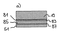
図2によると、本発明によるセンサヘッド11は、第1及び第2のセンサ領域29、35、支持プレート17及び評価器47を有する基材19を備える。基材19、支持プレート17及び評価器47は、接着剤及びアンダーフィルを用いて機械的に堅固に連結されており、環境に対して密閉されている。光源21は好ましくはLEDであり、光源のサイズを画定するダイアフラムの背後に配設される。本発明に関して、センサ及びダイアフラム49を好ましくは1回のエッチングプロセスによって形成する多段階薄膜プロセスにおいて、センサ領域29、35が基材上に直接配置されることが重要である。この製造方法は、ダイアフラム49とセンサ領域29、35の間の関係を極めて正確に確立することができ、これにより、これらを図3b及び図4bによる1つのエッチング段階で形成することができるという利点を有する。
According to FIG. 2, the sensor head 11 according to the invention comprises a
第1及び第2のセンサ領域29、35と支持プレート17の間の電気的接続は、好ましくはフリップチップ組立てによって提供される。いわゆる「スタッドバンプ」又は超音波によって設置される金の球体53のような電気的接触をアルミニウムで形成された最上部のセンサ領域51上に設置する(図3e)ため、製造プロセス中に、ハンダの「バンプ」を使用した場合に発生し得る熱感受性センサ領域29、35への損傷が発生し得ない。再び、回路基板コンダクタ55を支持プレート17上に設ける。これらの回路基板コンダクタ55の上側に、好ましくはフィルム57を設置し、このフィルム57は平坦な電気的接続箇所に凹部59を有し、この凹部59は組立て前に導電性接着剤54で充填される(図3e)。ここで、基材19及び支持プレート17をフリップチップ組立てを用いて連結することができる。非導電性層57には、意図した接点において凹部59が存在する。フィルム形成材としては、例えばエポキシ材料等の様々なプラスチックが適している。接着後、支持プレート17とガラス基材19の間の空間をいわゆる「アンダーフィル」で充填する。
The electrical connection between the first and
例えばASIC等のデコード回路47を、支持プレート17の背面63に配設する。デコード回路47もまた、ガラス基材19と支持プレート17の間の接続と同様、フリップチップ組立てによって、支持プレート17に接続される。この目的のために、回路基板コンダクタ64と、凹部67を有する非導電性層65とを、背面63に設置する。凹部67は、デコード回路47の接点に対応する。これらの凹部67を、支持プレート17とデコード回路47を連結する前に、導電性接着剤で充填する。支持プレート17の開口69によって、前面から背面までの完全な接触がもたらされ、この開口69は、例えばハンダ等の導電性材料、又は導電性接着剤で充填される。
For example, a
図2からわかるように、例えばLED等の光源21を、支持プレート17の凹部71内に格納する。スペーサ75により、光源21をガラス基材19から離間して保持し、これにより、光開口とダイアフラム49の間にエアギャップ77を設ける。このエアギャップ77は、光量のより良好な利用を達成するために、基材19に存在する内面反射を低減する働きをする。LED光源21の背面は、導電性接着剤79を用いて接触させることができる(図4e)。
As can be seen from FIG. 2, the
特に、センサ領域とダイアフラム49を薄膜技術で製造する様式は、本発明の応用において重要である。この様式では、第1のステップにおいて、センサ領域の構成のために必要な全ての層を、好ましくはガラス基材である透明な基材上の広範なエリア上に配置する(図3a)。ガラス基材のサイズは、特に200以上、好ましくは2000以上、特に好ましくは10000以上の多数のセンサの配設を同時に行うことができるように選択する。基材サイズの選択は、利用可能なコーティング及びエッチングデバイスに左右される。
In particular, the manner in which the sensor area and
光レシーバの製造では、好ましくは以下の層を連続してガラス基材19上に設置し(図3a)、好ましくはPINダイオード構造を生成する:
1)10〜100nm、好ましくは20〜70nm、特に好ましくは25〜50nmの層厚を有する、好ましくはTCO(透明導電性酸化物)層である導電性の透明な層81、
2)10〜80nm、好ましくは20〜70nm、特に好ましくは25〜50nmの層厚を有する、第1のn−又はp+ドープ層83、
3)100〜1500nm、好ましくは200〜1000nm、特に好ましくは400〜800nmの層厚を有する、真性層85、
4)10〜80nm、好ましくは20〜70nm、特に好ましくは25〜50nmの層厚を有する、第2のn−又はp+ドープ層87、及び
5)100〜2000nm、好ましくは500〜1500nm、特に好ましくは700〜1200nmの層厚を有する、導電性最上層51。接点89、91の領域、又はパッド111の領域(図10参照)では、層厚は特に好ましくは1000nmである。
In the manufacture of an optical receiver, preferably the following layers are placed in succession on the glass substrate 19 (FIG. 3a), preferably to produce a PIN diode structure:
1) a conductive
2) a first n- or p + doped
3) an
4) a second n- or p + doped
様々な層を、好ましくはCVD(化学蒸着)、PECVD(プラズマ増強化学蒸着)、又はVHFCVD若しくはHWCWD等の同様の改変したプロセスによって蒸着する。Si:h(非晶質シリコン)真性層を生成するための、好ましくはシランのプラズマ増強化学蒸着が好ましい。層のドープのために、シランは好ましくは他の気体の混合を有し、これは金属ゲルマニウム(例えばGeH)及び/又はホウ素(例えばBH)を含有する。 The various layers are preferably deposited by CVD (Chemical Vapor Deposition), PECVD (Plasma Enhanced Chemical Vapor Deposition), or similar modified processes such as VHFCVD or HWCWD. Plasma enhanced chemical vapor deposition of silane is preferred for producing a Si: h (amorphous silicon) intrinsic layer. For layer doping, the silane preferably has a mixture of other gases, which contain metal germanium (eg GeH) and / or boron (eg BH).
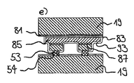
ガラス基材を上述の層でコーティングした後、最上層51にフォトレジストを設置し、これをマスクを用いてUVに曝露し、曝露されていない領域又は曝露された領域を溶解させることにより、光レシーバ要素及び光源の形状及び範囲を画定する。そして、例えばフォトレジストが溶解して除去される場所へのイオンビームエッチングによる第1のエッチングステップにおいて、第2のドープ層87及び好ましくは非晶質シリコン層85の一部を除去することができる。その結果、光レシーバの構造がここで既に形成される(図3b)。非晶質シリコンの代わりに、好ましくはPINダイオードを形成するために用いることができる、同様の材料を用いることもできる。
After coating the glass substrate with the layers described above, a photoresist is placed on the
続いて、更なるステップにおいて、本質的に第2のエッチングステップ(イオンビームエッチング及び/若しくは「反応性イオンビームエッチング」(RIE)、又は改変した方法)において非晶質シリコン層85及び第1のドープ層83をエッチングして完全に除去することにより、特定の場所においてTCO層を露出させる(図3C)。手順は第1のエッチングプロセスと同様とすることができ、即ち、加工すべきでない場所を初めにマスキングし、その後マスキングされていない場所を加工する。これらのプロセスステップは当業者には極めて良く知られたものであるため、ここでこれ以上詳細に説明する必要はない。露出された場所は、非晶質シリコン層85の除去後、光レシーバの1つの電気的接点89を形成する。他方の接点91は、導電性カバー層51によって形成される。
Subsequently, in a further step, the
そして、センサ領域を、好ましくはSiO2層である保護層93で好ましくはコーティングする(図3d)。接点89、91、各場合において、エッチング又は剥離プロセスによって設ける。図3及び4は製造プロセスの説明の役割のみを果たすものであり、図示した層厚は実際の層厚と一致しないことを指摘しておく。
The sensor area is then preferably coated with a
図4から分かるように、光源を形成するためのこの例示的実施形態で使用されるダイアフラムは、光レシーバ構造及び接触を製造するために用いたものと同様のプロセスステップによって製造することができる。光開口49を第2のエッチングステップにおいて設置し(図4c)、第1のエッチングプロセスで既に部分的にエッチングされた場所を更に、又は完全にエッチングする。
As can be seen from FIG. 4, the diaphragm used in this exemplary embodiment for forming the light source can be manufactured by process steps similar to those used to manufacture the optical receiver structure and contacts. A
この光開口49を通して、光が妨げられることなく基材19まで通り抜けることができる。アルミニウム層51のようないずれの更なる(透明でない)層もまた同じ場所に開口を有し、これにより、光の通過が妨害されないようになっている。このようにしてダイアフラムを形成し、これは有利にはLED21からの光の伝播を制限し、又は光源のサイズ若しくは寸法を画定する。
Through this
LEDをスペーサ75(図12も参照)上に載置することにより、最上層51上に接着することができる。スペーサ75により、基材19と光源21の間の画定された間隙が設けられる。このようにして、接着剤79のためのキャビティが(高い信頼性で)画定される。スペーサの高さは4〜50μm、好ましくは6〜12μmであり、好ましくは永久レジストから形成される。
By placing the LED on the spacer 75 (see also FIG. 12), it is possible to adhere the LED on the
最後に、センサ領域及び支持プレート17を、フリップチップ組立てによって電気的に接続する。同一のプロセスステップで、光源の前面を、詳細には図示していない回路基板コンダクタが形成された(接点)金属層51に接触させる。
Finally, the sensor area and the
ガラス基材19の厚さは1mmとすることができる。この厚さは好ましくは0.4〜0.6mmであり、好ましくは厚さ約0.16mmのガラス基材を高解像度エンコーダ用に用いることができる。
The thickness of the
図5は、ウェハの形状の大きな支持プレート97上に隣接して配設された多数のセンサヘッドの配置を示す。この図は、フリップチップ組立てによってキャリア材料97上に固定された基材19を示す。キャリア材料は非導電性材料の板であり、この板上には、事前のコーティングプロセスにおいて、光レシーバ及びでコード回路を有する多数の基材19と、光レシーバ及びデコード回路とを接触させるために、その前面及び背面に回路基板コンダクタが設置されている。光源21は、例えば接着によって直接ガラス基材19上に設置することもでき、キャリア材料97の凹部に一体化させることもできる。そして、デコード回路47をキャリア材料97の背面に載置することができる。デコード回路47の組立ても、フリップチッププロセスで行うことができる。光レシーバ要素23及びデコード回路47を有する基材19を、支持プレート17に同時に接続することができる。センサヘッド11又はガラス基材19をデコード回路47に接触させた時に、エンコーダ機能を既にテストすることができる。これは自動プロセスで行うことができる。その直後、好ましくはけがかれた(溝98)キャリア材料97を分解、鋸切断又は研削ディスクを用いて分割し、支持プレート17とする。好ましくは、キャリア材料はセラミック、特に黒色セラミックである。
FIG. 5 shows an arrangement of a number of sensor heads arranged adjacent to each other on a support plate 97 having a large wafer shape. This figure shows the
キャリア材料97の横方向縁部上に、ツールのピン96が係合できる2つの凹部99を設ける。凹部99及び対応するツールを用いて、様々なプロセスステップ中にキャリア材料97を正確に位置合わせすることができる。これによって、経済的な製造が可能になる。
On the lateral edge of the carrier material 97 there are two
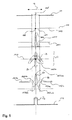
図6は、センサヘッドのコンパクトな設計のために、高品質センサを設置することができる、小型モータの例を示す。実量器上に図9による絶対トラック及び図7による増分トラックが存在する場合、アブソリュートエンコーダを同一の構成容積及び同一の構成で構成することができる。この場合、絶対位置を決定する、又はセンサヘッドを用いて実量器から読み取るためには、2°未満の動作で十分である。現行技術の(索引マークを有する)エンコーダでは、絶対基準位置を探すために360°までの角度動作が必要である。 FIG. 6 shows an example of a small motor where high quality sensors can be installed due to the compact design of the sensor head. If the absolute track according to FIG. 9 and the incremental track according to FIG. 7 are present on the actual meter, the absolute encoder can be configured with the same configuration volume and the same configuration. In this case, an operation of less than 2 ° is sufficient to determine the absolute position or to read from the actual meter using the sensor head. Current art encoders (with index marks) require angular movements up to 360 ° to find the absolute reference position.
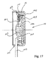
図6は、センサヘッド11及びロータリエンコーダ155を有するエンコーダ10を示し、その表面には実量器(図示せず)が配設される。ロータリエンコーダ155はシャフト157に接続され、従って回転可能である。センサヘッド11、及び光学素子(図示せず)から形成される実量器は、相互作用して信号を生成する。このために、この構成において、センサヘッド11は、実量器に向かって光を放出する光源21を有する。実量器の光学素子は、ロータリエンコーダ155の、センサヘッド11に対面していない側に配設される。これらは光源21から来る光をひとまとめにしてセンサヘッド11へと反射し、光はここで光レシーバ要素(図示せず)によって記録される。当然、光源はロータリエンコーダ155の他の側にも配設することができ、光学素子を介してセンサヘッド11へと光を送ることができる。しかしながら、センサヘッド11が1つ以上の光源と1つ以上の光レシーバ要素の両方を有する解決法が好ましい。位置信号の正しい形成のために、光レシーバ要素を光学素子に対して画定された位置に配設しなければならない。従来技術から公知のように、実量器又は筐体に対する光レシーバ要素の位置を直接ツール及び/又は光学デバイスを用いて調整する代わりに、図示したエンコーダ10において、これは、デバイスの独立した部分の寸法を互いに適合させることにより間接的に達成される。センサヘッドホルダ141は、開口149の形状の第1の構造要素を有し、センサヘッド11の一部を開口149に挿入して正確に嵌合させることができ、これにより固定接続が生成される。センサヘッド11のこの部分は有利には透明な基材19であり、好ましくはこの上に、光レシーバ要素を薄膜プロセスによって設置する。これらのプロセスでは、多数の光レシーバ要素を1つの基材板上に載置し、その後これを(より小さな)基材19に切断する。センサヘッド11のこのような設計により、基材の縁部に対する光レシーバ要素の位置を、基材板を正確に切断することにより決定することができる。基材19の縁部151は、センサヘッドホルダ141の上述の開口149と、固定接続として相互作用することができる。開口149は、ここではセンサヘッドホルダ141の縁部153にある第2の構造要素に対して正確に配置される。センサヘッドホルダ141の縁部153は、筐体143の内壁と、固定接続として相互作用することができ、ここで、筐体143を再び、実量器に対して画定された位置に配設する。これは、実量器上の光学素子に対するセンサヘッド11又は基材19の位置、従って光レシーバ要素の位置を、寸法に関して互いに適合されたデバイスの複数の部分によって間接的に確立することを意味する。その利点は、組立て中に機械的調整が一切必要ないことである。よって、センサヘッドホルダ141はアダプタとしても機能する。上述の寸法又は画定された位置に関して、偏差を確実に0.2mm未満、好ましくは0.05mm未満とするのが有利であり、これは一般に、測定デバイスを正しく機能させるのに十分である。筐体143をカバー145で密閉し、このカバー145はセンサヘッドホルダ141を押圧し、これによりセンサヘッドホルダ141を筐体143内に固定する。筐体143は好ましくは、カバー145と筐体143の間に開口を有し、この開口を通って、例えばケーブル159、好ましくはFlexprintを用いてセンサヘッド11の接触を発生させることができる。この配置は、センサヘッドの簡単な組立てを保証する。図6に示すエンコーダ10の好ましい構成変形例によると、ロータリエンコーダ155用のアダプタをシャフト157上に設ける。アダプタはシャフト用の着座部、及びシャフト157から径方向に外向きに延伸するフランジ241を有する。好ましくは、アダプタは中空円柱形シャフト支持体及びシャフト支持体から突出する環状フランジ241を有する。ロータリエンコーダ155は、シャフト支持体のシャフト157に対面していない側、及びアダプタのフランジ241と接触し、ロータリエンコーダが、エンコーダ10を組立てた状態においてフランジ241と接触する1つ以上の足240を有することが好ましい。ロータリエンコーダ155は、好ましくは接着剤を用いてアダプタ上に固定される。この配置は、センサヘッドの簡単な組立てを保証する。
FIG. 6 shows an
好ましくは、ロータリエンコーダ155をシャフト157に接着する。1つ以上のチャネル275(例えば2〜20又は3〜10)をロータリエンコーダとシャフト157の間に形成し、接着剤で充填するために、好ましくはロータリエンコーダの貫通孔272を構成する(図18)。図18は、ロータリエンコーダ155の貫通孔272の設計の1つを示し、ここでロータリエンコーダは平坦領域271を介したシャフト157との固定接続を有する。従って、貫通孔272の縁部の、チャネル275を形成する部分は、縁部の平坦領域271を形成する部分と比べて、シャフトから遠い(0.02〜0.2mm遠い)位置にある。好ましくは後者はシャフトと接しており、即ち平坦領域はロータリエンコーダ155とシャフト157の接点を表す。ロータリエンコーダとシャフト157の間のチャネル275を接着剤で充填することができる。この配置は、貫通孔272を設けるためのツールを極めて容易に製造できるという点で、ツールの製造者からすると特に有利である。上記ツールは、シャフト157の直径より0.02〜0.2mm大きい直径を有する(好ましくは円柱)ワークピースから作製するのが有利である。このワークピースは、例えば研削によって、貫通孔272の製造中に平坦領域271を形成する、平坦部又は平坦側面を有する複数の場所に設けることができる。好ましい構成変形例によると、1〜10、特に2〜5、特に好ましくは3つのチャネル275を設ける。
Preferably, the
ロータリエンコーダ及び実量器は好ましくはプラスチックで形成され、好ましくは容易に目視検査できるよう、黒色プラスチックで形成される。そして、実量器を金属、好ましくは金又はアルミニウムでコーティングする。しかしながら、例えばSiO2又は合成樹脂の追加の保護層をアルミニウム層上に設置することができる。 The rotary encoder and meter are preferably made of plastic, preferably black plastic for easy visual inspection. The actual meter is then coated with a metal, preferably gold or aluminum. However, an additional protective layer of eg SiO 2 or synthetic resin can be placed on the aluminum layer.
代替実施形態として、ロータリエンコーダのフィルム構造を想定することができる。プラスチックはキャリア材料としての役割を果たすことができ、アルミニウム層及びアルミニウム層の酸化保護用プラスチックフィルムをこの上に設ける。実量器は、アルミニウム層の側面への加熱型押しによって形成することができる。 As an alternative embodiment, a rotary encoder film structure can be envisaged. Plastic can serve as a carrier material, and an aluminum layer and a plastic film for oxidation protection of the aluminum layer are provided thereon. A real meter can be formed by hot stamping on the side of the aluminum layer.
図7、8及び9は、実量器25/31、及び少なくとも1つのアナログ信号103を形成する役割を果たす光レシーバ要素23の、様々な実施形態を示す。アナログ信号103a及び103bは、デコード回路で処理され、任意で、更に処理することができるデジタル信号104に変換される。デコード回路からの出力信号は、センサヘッドに対する実量器の位置の決定に役立つ。位置データをアナログ又はデジタル信号を用いて評価することができる。
FIGS. 7, 8 and 9 show various embodiments of a
図7は増分トラックを示し、図8は索引を形成するためのトラックを示し、この索引は1回転あたり少なくとも一度評価され、図9は別のトラック構造を示し、これはマンチェスターコードに従ってエンコードされ、増分信号とトッモに絶対位置を画定することができる。上述の3つのトラックは、別個に又は組み合わせて、実量器を形成し、この実量器は、例えばロータリエンコーダ等のキャリア上に一体化することができ、好ましくはキャリアと同一の動作で作製される。実量器は好ましくは2つのトラックで形成され、両トラックの光学素子は好ましくは同一の焦点距離を有する。 FIG. 7 shows an incremental track, FIG. 8 shows a track for forming an index, this index is evaluated at least once per revolution, FIG. 9 shows another track structure, which is encoded according to Manchester code, Absolute positions can be defined for incremental signals and toms. The above three tracks, separately or in combination, form a real meter, which can be integrated on a carrier, for example a rotary encoder, preferably made in the same operation as the carrier Is done. The actual meter is preferably formed of two tracks, and the optical elements of both tracks preferably have the same focal length.
図7に示す実量器のトラック25は、独立した光学素子からなり、これらの光学素子は互いから規則的な距離だけ離れて移動方向15に配設される(増分トラック)。これらは、これらから反射される光の主方向と同じ方向又はこれに対して平行に配向される。図7では、光学素子は半円柱反射器であり、これは本発明の文脈における好ましい実施形態を表す。光源から放出された光は、実量器の光学素子によってひとまとまりにされ、センサ100の平面上に集中する。ここで、光は点108に入射する。しかし、センサの平面の隣接する領域107には光は殆ど又は全く入射しない。センサの平面上の光強度の分布をカーブ101で表す。カーブの点101hは高エネルギ密度に対応し、点101tは低エネルギ密度に対応する。光強度から電気信号への電気的変換を、好ましくは互いに180°変位して配設される少なくとも2つの光レシーバ要素23によって行う。これは、1つの光レシーバ要素が最大値を記録する場合に他方の光レシーバ要素は最小値を記録し、またその逆も成り立つことを意味する。2つの光レシーバ要素を用いて、2つのアナログ信号103A+及び103A−を生成し、これらを更なる処理のためにデコード回路に送る。そして、デコード回路はアナログ信号103からデジタル信号104を形成することができる。
The
図8は、軸105付近を中心とするおよそ半円柱状の断面を有する単一の反射器からなる実量器の索引トラック31を示す。この反射器の幅は、増分トラックの反射器の幅の100〜300%とする。センサ100の平面上において、光は基本的に点108においてひとまとまりにされ、隣接する領域107には極めてわずかな光しか入射しない。本質的に一定で変調されない量の光が、残りの領域109に入射する。センサ100の平面上の光強度の分布をカーブ101で示し、点101hは高エネルギ密度に対応し、点101tは低エネルギ密度に対応する。光強度から電気信号への変換を、好ましくは光レシーバ要素23の特別な配置によって行う。好ましい実施形態によると、光レシーバ要素23は主レシーバ23Z+、及び主レシーバ23Z+に対して対称に配設されかつ共に電気的に接続される2つのレシーバ23Z−からなる。有利には、光レシーバ23Z−の総面積は、主レシーバ23Z+の総面積より少なくとも10%、好ましくは少なくとも20%、特に好ましくは少なくとも30%大きい。これは、信号の評価に関連して重要である。2つの光レシーバ要素Z+/Z−の面積が異なることから、信号103aを信号103bから確実に十分遠ざけることができ、これにより、残りの領域109においてこれらが絶対に交差しないようにすることができる。光レシーバのこの配置により、2つのアナログ信号103a及び103bを生成し、これらをデコード回路で更に処理する。これらの信号は例えば比較器回路で比較することができ、ここで、2つの信号の交差点は、各場合においてデジタルレベルの変化、即ちパルスZbのフランクの1つを生成する(デジタル信号104を参照)。
FIG. 8 shows a real
安定したデジタルパルス104を形成するために、2つの信号103a及び103bが大きな傾斜部で交差することが重要である。これは、光レシーバ要素23の特別な配置によって達成される。図8による中心位置において、ひとまとめにされた光ビームは主に中央のレシーバ要素23Z+に入射し、これにより信号ピーク103aaが形成される。信号レベル103baが可能な限り低くなるように、2つの光レシーバ要素Z−は、例えば点107において、通常より少ない光、即ち光ビームが変調されていない場合より少ない光を受けるようにする。これは、上部、即ち近位端上に形成された、斜めに配置された光レシーバ要素が、遠位端におけるよりも若干幅広であることによって達成される。図示したレシーバ23Z+、23Z−、即ち、第1の楕円形光レシーバ要素23Z+と、本質的に鏡像対称に、かつ第1のレシーバ要素23Z+の長手方向軸に対して角度を付けて配設された2つの第2の楕円形光レシーバ要素23Z−とを、最適なものと見なすことができる。光レシーバ要素のこの形状により、相互に交差する点において大きな傾斜部を有する信号103a及び103bを形成することができ、これにより、索引信号のために信頼性の高い基本信号Zbを形成することができる。
In order to form a stable
光レシーバ要素Z−(「Zマイナス」)を、光レシーバ要素Z+(「Zプラス」)に対して斜めに配設する。光レシーバ要素Z+に対面していない端部における光レシーバ要素Z−の幅は、光レシーバ要素Z+に対面する端部における幅よりも非常に小さい。この最適な配置は、方向15への索引レンズ(実量器上の光学素子)の移動中、中間の光強度、低い光強度、及び高い光強度がセンサ領域にわたって移動することを意味する。光レシーバ要素Z−のこの形状は、光強度領域の変化が、センサ領域に対する索引レンズのいずれの位置において、信号に同じ程度に影響することがないことを意味している。縁部領域、即ち光レシーバ要素Z−の狭い端部が検知する領域では、中央領域、即ち光レシーバ要素Z+が位置し、光レシーバ要素Z−の幅広い端部がある領域に比べて、光強度は信号に対して弱い影響しか持たない。別の因子は、光源からの距離である。光レシーバ要素Z−の狭い端部は、光源からより離れており、従って弱い光強度を受けることになる。
The optical receiver element Z− (“Z minus”) is disposed obliquely with respect to the optical receiver element Z + (“Z plus”). The width of the optical receiver element Z− at the end not facing the optical receiver element Z + is much smaller than the width at the end facing the optical receiver element Z +. This optimal placement means that during the movement of the index lens (optical element on the real meter) in
好ましくは、2つの光レシーバ要素23Z+及び23Z−の幾何学的重心102bは、可能な限り同一の点で一致する。重心が一致しない場合、即ちこれらがいくらかの距離だけ離間している場合、2つの信号103aと103bの間のレベル比は、実量器13と基材19の間の距離が変化すると変化する(図1参照)。レシーバ要素23の上述の有利なジオメトリにより、実量器とセンサヘッドの間の距離は、信号の品質に悪影響を及ぼさずに、比較的広い範囲にわたって変化することができ、これにより、小さなモータのシャフトの軸方向位置について、何の問題もなくかなり大きな許容誤差をとることができる。これはまた、コストのかかる調整が必要でないという利点も有する。
Preferably, the geometric centroids 102b of the two optical receiver elements 23Z + and 23Z- coincide as closely as possible. If the centroids do not match, i.e. they are separated by some distance, the level ratio between the two
図9は、実量器のトラック31(絶対トラック)を示す。このトラックは、図7に示した増分トラックと同様、多数の光学素子を含むが、ここでは、光学素子はその全てが同一に若しくは規則的に整列しておらず、又は(それらの光軸に対して)全てが平行ではない。各光学素子は、センサの平面上の第1又は第2の点に光を集中させるように構成及び/又は配設される。2つの点は、バイナリコードの0(ゼロ)又は1(一)を表す。ゼロ及び1のシーケンス(2進数字)は、例えば8ビットコード等のコードを定義し、8ビットコードでは、8つの連続した2進数字が、実量器上又は実量器の長さにわたって好ましくは1度だけ発生する特徴的な位置番号を定義する。本実施例では、1つの点は軸105の左にあり、他方は軸105の右にある。しかしながら、3つ以上の異なる点を設ける、つまり、センサ100の平面上の異なる位置にある入射点108のシーケンスが例えば3進コードを形成するように、光学素子を配設及び/又は構成することもできる。しかしながら、バイナリコード、特にいわゆるマンチェスターコードが好ましい。センサ100の平面上において、光は点108でひとまとまりにされ、この点108は各場合において軸105に関して非対称に配設される。そして、領域107にはわずかな量の光しか当たらない。センサの平面上の光強度の分布を、カーブ101で示す。光強度から電気信号への電気的変換を、好ましくは互いに180°変位して配設される少なくとも2つの光レシーバ要素23によって行う。光レシーバ要素23を用いて、2つのアナログ信号103a及び103bを生成し、これらを増分信号と共にデコード回路に供給する。増分信号の助けで、デコード回路は信号103を評価し、これにより区画のビット値を決定し、デジタル信号で出力することができる。
FIG. 9 shows a track 31 (absolute track) of the actual quantity device. This track, like the incremental track shown in FIG. 7, contains a number of optical elements, but here the optical elements are not all aligned identically or regularly, or (on their optical axes). In contrast, everything is not parallel. Each optical element is configured and / or arranged to concentrate light at a first or second point on the plane of the sensor. Two points represent binary code 0 (zero) or 1 (one). A sequence of zeros and ones (binary digits) defines a code, such as an 8-bit code, for which 8 consecutive binary digits are preferred on the actual meter or over the length of the actual meter Defines a characteristic position number that occurs only once. In this example, one point is to the left of the
有利には、2つのチャネル(A及びB)と、1つのチャネルあたり2つの上述の光レシーバ要素23とを設ける。わかりやすくするために、図7及び9では、各場合において1つのチャネル(A又はB)の光レシーバ要素23のみを示していることに留意されたい。
Advantageously, two channels (A and B) and two above-mentioned
15による実量器の移動又は回転の所定の方向に関して、この時点での信号103aと103bの間の差を読み取ることにより、ビット値を2つの増分信号の各上昇又は各下降フランク上で、好ましくは(チャネルA及び/又はBから)2つの増分信号のフランク4つ毎に読み取る。この時点で、デジタル信号181のレベルをビット値に従って調整するか、ビット値をその他の方法で出力する。実量器の回転方向又は移動方向におけるビット値を読み取ることは、例えば、チャネルAの下降フランクを用いて行われ、また、反対方向の回転又は移動についてはチャネルAの上昇フランクを用いて行われることも想定可能である。
By reading the difference between the
2つの増分信号は、区画あたり4つのフランクを形成する(チャネルA/Bあたり2つのアナログ信号103a/103b)。ビット値を評価するためにこれらのフランクのどれを用いるかは、最終的に、角度41に関する回転に対する、許容可能な許容誤差フィールド内でのセンサヘッドの配置に左右される(図1参照)。角度誤差は、図13に示す回路を用いて補正することができる。
The two incremental signals form four flanks per partition (two
上述のように,実量器のビット値の順序は、特定の数の連続するビットを用いて、特定の順序は実量器の長さにわたって1度しか表れることができないように選択される。好ましくは、順序はマンチェスターコードに従って形成される。 As described above, the order of the bit values of the real quantity is selected so that the specific order can only appear once over the length of the real quantity using a specific number of consecutive bits. Preferably, the order is formed according to the Manchester code.
図10は、3チャネルエンコーダ(チャネルA、チャネルB、チャネルZ又は索引)用光レシーバ要素23の配置を示し、光源の中心を通る、放出される光ビームの主軸45は、実量器の中心線43と一致する(図1、2)(図1参照)。増分信号のための光レシーバ要素を(実量器の第1のトラック25と相互作用する)センサ領域29に配設し、索引信号のための光レシーバ要素を(実量器の第2のトラック31と相互作用する)センサ領域35に配設する。接点又は開口91(図3d及び3eも参照)において、例えば超音波溶接によって、「スタッドバンプ」を最上部の金属層(図3aの51参照)に配設することができる。これらの点を金の層でカバーすることができ、これにより、導電性接着剤を用いる場合に、接着性が酸化物層によって損なわれずにすむ。マンチェスターコードによるアブソリュートエンコーダのために同一のセンサヘッドを使用することもでき、領域25は変化しないままであり、(例えば図9にみられる)少なくとも2つのレシーバ要素は領域31に配設される。
FIG. 10 shows the arrangement of the
エンコーダを組立て許容誤差に対して(即ち、光源のセンタリング及び実量器の主軸43(図1参照)に対するセンサヘッドの角度位置に関して)非感受性とするために、好ましくは、移動方向15に関して光レシーバ要素の以下のような順番を選択する:A+/B−/A−/B+又はA−/B+/A+/B−、即ち、2つのチャネルA及びBに関して、光レシーバ要素が軸39に関して対称に配設される。この場合、光レシーバ要素A+、A−及びB−、B+は、各場合において、180°だけオフセットしている。このようにして、チャネルA及びチャネルBの両方に関して、互いに180°だけ変位した2つの正弦曲線が得られ、これを比較器回路においてデジタル信号に変換することができる。この配置では、光レシーバ要素23の間の接点及び連結は、光レシーバ要素と同じ材料で形成されるか、同じ材料から形成され、即ち、これらの領域は光電子工学的にアクティブでもある。そして、センサ領域29内の4つの光レシーバ要素のそれぞれの重心は、光源21から本質的に等距離にある(線102参照)ことに留意する必要がある。ここで、点102bは各場合においてU字型レシーバ要素の重心をマークする。方向15において、重心102b間の距離は実量器の区画と本質的に一致することになる。センサ領域29内の光レシーバの通常の幅114は、好ましくは実量器の区画の幅の40〜80%の間で選択する。この文脈では幅とは、主軸45に平行に走る光レシーバ要素又は光源の寸法として理解される。光レシーバ要素のアレイの重心を正しい位置で得るために、一般に、レシーバ要素の幅を、特定の場所106において幅広くするか、又は幅を調整する必要がある。これは、光レシーバ要素内の転移線115及び接点又は開口91の周りの領域もまた光を検知し、つまり、光レシーバ要素の面積を必然的に増大させるためである。これは光レシーバ要素の重心102bの位置及び生成される信号にマイナスの影響を与えるものである。参照符号110は、TCO層への接触を示す。
In order to make the encoder insensitive to assembly tolerances (i.e. with respect to the centering of the light source and the angular position of the sensor head with respect to the
有利には、光源21又はダイアフラム49の幅を、区画の幅の60〜150%、好ましくは100〜120%に選択する。ダイアフラム49の幅が小さすぎると、あまりにわずかな光しか通過できない。ダイアフラム49の幅が大きすぎると、光のスポットの幅が大きくなり過ぎ、信号が平坦になり過ぎて信頼性の高い評価ができなくなる。
Advantageously, the width of the
例えば光源21が基材19上で発光OLEDとして構成され、センサ領域35及び29がOLEDと同一の層構造を持つようになっている場合、光源及び光レシーバ要素の同様の配置を、他の技術によって達成することができる。OLEDと光レシーバ要素の両方は、好ましくは図3aに示すような薄い層からなるが、異なる開始材料を使用することもできる。
For example, if the
図11は、光レシーバ要素の別の配置を示し、ここでは独立した光レシーバ要素をVIA112(「垂直相互接続アクセス」)を用いて、パッシベーション層(例えばSiO2層又はSiO2/Si3N4層構造)を通して、パッシベーション層上に設置した好ましくはアルミニウムの導電性トラックと電気的に接続する。この配置の利点は、転移線115及び/若しくは接点91がアナログ信号の形成に影響を及ぼすことができるようにすることなく、又は、幅114の補正を必要とすることなく、光レシーバ要素23が最適に構成されることである。導電性トラックの端部にパッド111が存在し、その上に「スタッドバンプ」を設置する。このような解決法は、追加の層を設けなければならず、更なる用心を払わなければならないため、よりコストがかかる。移動方向15におけるレシーバ要素23の配置は、図10の説明において上で挙げたものと同一の利点を有する。TCO層への接続は、導電性トラック及びVIA112を用いて行うこともでき、ここで、スタッドバンプの信頼性の高い設置のために、パッド111を再び導電性トラックの端部に配設することができる。
FIG. 11 shows another arrangement of optical receiver elements, where an independent optical receiver element is used with a VIA 112 (“Vertical Interconnect Access”) and a passivation layer (eg, SiO 2 layer or SiO 2 / Si 3 N 4). Through a layer structure) and electrically connected to a conductive track, preferably aluminum, placed on the passivation layer. The advantage of this arrangement is that the
図12は、ダイアフラム及びLEDからなる光源の好ましい設計を示す(図2も参照)。図4cで説明したように、LEDは基材19(好ましくはガラス製)上又は最上部の金属層(図3の51参照)上に接着され、薄膜構造で作製された光開口49を通して光を放射する。LED21を支持プレート17(図2参照)の凹部71(図2参照)に格納する。光源を基材19上に設置できる方法の複数の変形例を示す。図12aは、放出層161及び接触層163を有する光源を示す。光源21と、コーティングされたガラス基材19との間には、光源を基材19から離間して保持するスペーサ75を設ける。この設計を用いる場合、横方向に出現する光165が光レシーバ上に衝突するリスクがある、即ち、この配置には、生成された散乱光が光センサ領域に進入することができ、これにより、所望の信号品質からの偏差が発生し得るという不利益がある。参照番号170は、光源から実量器へ放出された光のコーンを示す。
FIG. 12 shows a preferred design of a light source consisting of a diaphragm and LEDs (see also FIG. 2). As described in FIG. 4c, the LED is glued on the substrate 19 (preferably made of glass) or on the uppermost metal layer (see 51 in FIG. 3) and transmits light through a
図12bは、放出層161の縁部を不透明なカバー層167でコーティングした、隔離された光源を示す。これは、散乱光が光レシーバに衝突するのを防止できる。図12cによると、不透明なカバー層167を光源21上ではなく光レシーバ上に設置する。このカバー層は、例えばLEDへの接触163としても機能する。「アンダーフィル」として、不透明な、又は低い光透過性を有する材料を選択するという更なる用心が必要となり得る。
FIG. 12 b shows an isolated light source with the edge of the
図13は、実量器の主軸に対するセンサヘッドの角度位置41(図1参照)に関する組立て誤差を補償できる回路を示し、これにより、上記角度誤差に関わらず、索引信号が高い信頼性で機能することができる。上述のように、ビット値を(絶対トラックと関連して)決定するための増分信号のフランクの選択は、センサヘッドの配置又はセンサヘッドの角度41の回転に左右される。従って、この回路を用いてこれらのフランクを決定することができる。
FIG. 13 shows a circuit capable of compensating for an assembly error related to the angular position 41 (see FIG. 1) of the sensor head with respect to the spindle of the actual measuring device, whereby the index signal functions with high reliability regardless of the angular error. be able to. As mentioned above, the selection of the flank of the incremental signal to determine the bit value (relative to the absolute track) depends on the sensor head placement or
図13aは、信号A、B、Zb及びZを示す。信号Zは、信号A及びB及びZbを組み合わせることで形成される。A及びBはそれぞれデジタル信号181に対応し(1チャネルに対する信号のみを示す図9を参照)、信号AはチャネルAから、信号BはチャネルBから発生する。上記図13aに示す信号Zは2つのパルスからなり、この信号Zは基本的には望ましくないものである。原信号A及びBを組み替えることにより、図13bにおいて、別の信号状態Aout(又はAo)及びBout(又はBo)が生成され、信号Zbは信号A及びBの領域に、プラスにほぼセンタリングされる。従って、結果として得られる信号Zは単一のパルスからなる。 FIG. 13a shows the signals A, B, Zb and Z. Signal Z is formed by combining signals A and B and Zb. A and B each correspond to a digital signal 181 (see FIG. 9 which shows only the signal for one channel), signal A originates from channel A and signal B originates from channel B. The signal Z shown in FIG. 13a consists of two pulses, which is basically undesirable. By rearranging the original signals A and B, in FIG. 13b, another signal state Aout (or Ao) and Bout (or Bo) is generated, and the signal Zb is approximately centered positively in the region of signals A and B. . Thus, the resulting signal Z consists of a single pulse.
原信号A(又はAin)及びB(又はBin)の、効果的な出力信号Aout及びBoutへの変換(組み替え)は、制御信号X1及びX2を用いて、例えば図13cの組み合わせ表に従って行われ、ここで原信号A及びBは反転される及び/又は交換される。 The conversion (recombination) of the original signals A (or Ain) and B (or Bin) into effective output signals Aout and Bout is performed using the control signals X1 and X2, for example, according to the combination table of FIG. Here, the original signals A and B are inverted and / or exchanged.
図13bの2つのチャネルA及びBは、チャネルAに関しては反転された入力チャネルB、チャネルBに関しては入力チャネルAからなる。従って、チャネルAout及びチャネルBout及びチャネルZbからの信号を組み合わせることにより、単一のパルスを有する索引信号Zが形成される。更なる信号の組み合わせを、真理値表13cに示す。 The two channels A and B in FIG. 13b consist of an inverted input channel B for channel A and an input channel A for channel B. Therefore, by combining the signals from channel Aout, channel Bout and channel Zb, an index signal Z having a single pulse is formed. Further signal combinations are shown in truth table 13c.
真理値表に従った信号処理は、図示した回路によって行うことができる(図13d)。回路を2つの制御信号X1およびX2で制御する。信号Ain200及びBin201を2つのインバータ206、207で反転させる。回路は更に、4つのマルチプレクサ208を含み、これらは、制御信号X1、X2の状態に応じて、入力における2つの信号のうち1つを出力に中継する。図13a及び13bに示す例では制御信号はX1=0及びX2=1に設定され、図13dでは移動を太線で示す。制御信号X1及びX2は、デコード回路で生成される。デコード回路は、最終的な製品検査において生じる、制御信号に関する様々な設定及び値をその中にプログラムできるように設計される。
Signal processing according to the truth table can be performed by the illustrated circuit (FIG. 13d). The circuit is controlled by two control signals X1 and X2. The signals Ain200 and Bin201 are inverted by the two
図14では、アブソリュートエンコーダの特別な設計を概略的に示しており、これは静止状態のセンサヘッド11若しくは静止状態のシャフト157について、又はコールドスタートにおいてさえ、絶対位置信号を決定することができる。これは、実量器とセンサヘッドとの間の相対移動を可能とする特別なデバイスによって可能となる。デバイスはスイベルアーム182(又は同等のデバイス)を有し、少なくとも1つのセンサヘッドがその上に固定される。スイベルアームはモータで駆動され、実量器13とセンサヘッド11の間の相対移動を生成し、これは、全回転の好ましくは5°未満のある画分に対応する。絶対位置を、センサヘッド11から来る信号を評価することによって決定することができる。センサヘッドのコンパクトな設計、及び許容誤差に寛容なこの配置の設計により、再びこれが可能となる。
FIG. 14 schematically shows a special design of an absolute encoder, which can determine the absolute position signal for a stationary sensor head 11 or a
図14は、筐体143、145、設置されたシャフト157、実量器13を有するロータリエンコーダ155、及び、少なくとも1つのセンサヘッド11を設置した、固定された又は小さな角度だけ旋回できるキャリア182を有するアブソリュートエンコーダの概略的な構成を示し、ロータリエンコーダ155は実量器13を有し、この実量器13は好ましくは図9による絶対トラック及び図7による増分トラックを有する。ロータリエンコーダ155をシャフト157上にセンタリングして固定し、筐体143内の上記シャフトは、少なくとも1つの軸受180との固定接続を有する。
FIG. 14 shows a
軸の小さな移動、又はロータリエンコーダの好ましくは3°未満の移動により、位置番号を決定することができ、この位置番号を用いて、ロータリエンコーダの(絶対)位置値を決定することができる。そして、位置値を、パルスを増分トラックに足す/から引くことにより、又は更なる位置番号を決定することにより、決定することができる。位置値の冗長取得は、3つの変形例を組み合わせることによって容易に達成できる。 The position number can be determined by a small movement of the axis or by a movement of the rotary encoder, preferably less than 3 °, and this position number can be used to determine the (absolute) position value of the rotary encoder. The position value can then be determined by adding / subtracting the pulse to the incremental track or by determining a further position number. Redundancy acquisition of position values can be easily achieved by combining three variations.
好ましくは、1対以上のレシーバ要素を用いてマンチェスターコードを読み取る(図9参照)。位置番号は、センサヘッドに対する実量器の移動によって、1から位置番号の最大値までの間で決定される。バイナリ形式で表現される位置番号の長さは、ビット数であり、これが実量器の長さを決定する。位置番号を、多くの連続するビットを読み取ることにより決定する。位置番号を、マンチェスターコードに従って形成された実量器により画定する。実量器の全長において、位置番号は一意的であり、即ち、各場合において光レシーバに対する実量器の位置を決定する。読み取った位置番号は、デコード回路を用いて位置値に変換される。好ましくは、位置番号を、デジタル信号181を用いて送り、変換回路187を用いて位置値に変換する。変換回路187はデコード回路47と一体化することができる(図2も参照)。
Preferably, the Manchester code is read using one or more pairs of receiver elements (see FIG. 9). The position number is determined between 1 and the maximum value of the position number by the movement of the actual meter relative to the sensor head. The length of the position number expressed in binary format is the number of bits, which determines the length of the real quantity device. The position number is determined by reading many consecutive bits. The position number is defined by a real meter formed according to the Manchester code. In the total length of the real meter, the position number is unique, i.e. in each case determines the position of the real meter relative to the optical receiver. The read position number is converted into a position value using a decoding circuit. Preferably, the position number is sent using a
複数の連続した位置番号を記録することにより、位置値の冗長決定を読み取り誤差に対して保護することができる。これは、実際には「長さを延ばした」位置番号を記録することを意味する。長さを延ばした位置番号を、複数の位置値に変換する。位置値を一列に配置することができない場合、マンチェスターコードの読み取り誤差が存在すると結論付けることができる。 By recording a plurality of consecutive position numbers, redundancy determination of position values can be protected against reading errors. This actually means recording the “extended length” position number. The position number obtained by extending the length is converted into a plurality of position values. If the position values cannot be arranged in a row, it can be concluded that there is a Manchester code reading error.
図14は、変換回路187をセンサの外部に配設した配置を示す。変換回路186をエンコーダ又はそのデコード回路へ、3つの線186で接続する(概略的な描写)。2つの線は、チャネルA及びBからのパルス(デジタル信号104)を伝送し、第3の線は、絶対トラックの位置番号を形成するデジタル信号181を伝送する。このようにして、位置情報はエンコーダ10と変換回路187の間で冗長に伝送される。これにより、位置番号の信頼性の高い伝送と、位置値の信頼性の高い決定とが保証される。変換回路187は、SPI、I2C、Profibus等の慣用のデータバスを用いて、データを例えばSPS制御システムまで更に伝送する。好ましくは変換回路187はマイクロプロセッサ188を備え、これは位置番号の位置値への翻訳を実行する。位置番号の位置値への翻訳は、2つの異なる方法で行うことができる:
a)マンチェスターコード生成器が位置番号を連続的に形成する;翻訳される実量器からの位置番号の1つが、生成された位置番号と一致する場合、生成器の位置番号が位置値として出力される。
b)マイクロプロセッサにおいて、位置値を含む表が提供され、ここで、表中の各ストレージ位置又は各位置値は、特定の位置番号と関連しており、これにより、位置番号を特定の位置値に割り当てることができる。
FIG. 14 shows an arrangement in which the
a) Manchester code generator continuously forms position numbers; if one of the position numbers from the actual quantity being translated matches the generated position number, the position number of the generator is output as a position value Is done.
b) In the microprocessor, a table containing position values is provided, where each storage location or each position value in the table is associated with a specific position number, whereby the position number is converted to a specific position value. Can be assigned to.
マンチェスターコードを用いる慣用のエンコーダシステムの不利な点は、絶対位置の決定に関して、絶対位置値を決定するために、実量器の相対移動、及び従って測定される機械構成部品の移動が必要となることである。これは機械製造者にとってありがたくないことである。 The disadvantage of the conventional encoder system using the Manchester code is that with respect to the determination of the absolute position, the relative movement of the actual measuring device and thus the movement of the machine component to be measured is required to determine the absolute position value. That is. This is unfortunate for machine manufacturers.
いずれの移動が起こる前に、機械のスイッチングにおいて位置値を決定することができることが望ましい。これは、ロータリエンコーダが多数のトラックを有し、各トラックに少なくとも1つのレシーバ要素を割り当てることで解決される。このために必要な回路は複雑であり、このような多トラック配置は多くの空間を占有し、このため、この種の位置測定デバイスは小さな筐体に適合しない。 It is desirable to be able to determine position values in machine switching before any movement occurs. This is solved by the rotary encoder having multiple tracks and assigning at least one receiver element to each track. The circuitry required for this is complex and such a multi-track arrangement occupies a lot of space, so this type of position measuring device does not fit into a small housing.
本発明の別の実施形態では、実量器に対するセンサヘッドの移動をセンサの内部で可能にし、これにより、位置の決定を、機械を始動させることなく、ボタンを押すことによって行うことができる、手段が提供される。これは、センサヘッド又はセンサヘッドを配設するキャリア(例えばスイベルアーム182)を約3°にわたって方向転換させることにより達成される。これは例えばモータ185及びカム184を用いて行うことができ、カムは好ましくはスイベルアーム182のスロット183内で固定接続として係合する。レバー及びカムを有するモータの代わりに、異なる種類のアクチュエータを使用することができる。そして、この移動によって生成される信号(チャネルA、チャネルB及びM-コード)を、位置値の決定のために使用することができる。
In another embodiment of the invention, the movement of the sensor head relative to the actual meter is enabled inside the sensor, so that the position determination can be made by pressing a button without starting the machine, Means are provided. This is accomplished by turning the sensor head or carrier (eg, swivel arm 182) on which the sensor head is disposed over about 3 °. This can be done, for example, using a
図15〜17は、位置測定デバイスを示す。これは特にコンパクトな設計のエンコーダ10のキットである。この設計は、ロータリエンコーダ155、その上に設置された実量器、筐体143、及び実量器13と相互作用して信号を生成するセンサヘッド11の特定の配置を特徴とする。この場合、実量器13はロータリエンコーダ155の、筐体143に対面していない側249に配置される。これは好ましくは、筐体143の一部が、ロータリエンコーダ155及び/又は筐体143の上部の平坦な側に接して、これに沿って、又は本質的にこれと平行に延伸することを意味する。よって、ロータリエンコーダ155は好ましくは、筐体143の内側(又は筐体の上述の部分の内側)と、センサヘッド11又はプリント回路基板251との間に配設される。シャフト用の支持体267(又は、シャフト支持体の長さの少なくとも大部分、特に少なくとも70〜90%)が、ロータリエンコーダ155の、実量器13と同じ側に配設されているという事実から、かなりの空間が節約される。この理由は、測定の位置、即ち実量器13とセンサヘッド11の間の領域が、シャフト又はシャフト支持体267に接して配設されていることである。筐体143にロータリエンコーダ155を組付ける間、ロータリエンコーダ155に平行な筐体143の上述の部分に対するロータリエンコーダ155の位置、又は筐体143の内側とロータリエンコーダ155の間の距離は、筐体143の上述の平行な部分を押し込む又は変形させ、ロータリエンコーダ155の設置後にそれを再び解放することによって確立される。これを容易にするために、ロータリエンコーダ155と平行に走る、筐体143の上述の部分の材料を、隣接する部分より薄くするか、又はより弾性とすることができる。有利には、センサ11を、筐体143との固定接続を有するプリント回路基板251上に設置する。プリント回路基板251はまた、支持プレートの機能を確実なものとするように設計することができる。
15-17 show a position measuring device. This is a kit of the
特に好ましくは、これはスナップ接続153を用いて行われる。エンコーダ10の極めて容易な組立ては、第1の留め具257及び第2の留め具259を有するアダプタ部分255を用いて達成することができる。好ましくは、第1の留め具257は、アダプタ部分255をシャフトに対してモータ243の中心に固定する役割を果たし、例えばネジからなるものとすることができる。第2の留め具は有利にはスナップ接続259であり、これは例えば1つ以上の突出部261及び1つ以上の凹部263で形成される。突出部261及び凹部263を、筐体(特に筐体の内壁)及び/又はアダプタ部分255上に配設することができる。これは好ましくは着脱可能な接続である。有利には、筐体143は、ロータリエンコーダ155及び/又はロータリエンコーダ155に接続されたシャフト用の支持体267を受容するためのアセンブリ軸受265を有する。これは、ロータリエンコーダ155及びシャフト支持体265を、好ましくはワンピースで形成することができ、又は、共に接続される独立した部分とすることもできることによる。アセンブリ軸受265は、アセンブリ動作中、ロータリエンコーダを筐体の中心に保つ機能を有する。軸受自体は、ボール軸受又はテフロン製のスライド軸受とすることができ、モータシャフトの回転を負担しないため後者が好ましい。
Particularly preferably, this is done using a
アセンブリ軸受の機能は、ロータリエンコーダ及びセンサヘッドの正確な整列を保証することである(図1の軸22参照)。軸受の材料であるテフロンは、低い摩擦係数及び特に顕著なクリープ挙動という利点を有し、これにより、組立てられた状態において、軸受機能は時間を経ることで失われる。アセンブリ軸受は、存在する軸受システムがいずれの追加の不都合な負荷にさらされることがないように、組立て後にその軸受機能を失うべきであるため、これは望ましい。堅固な軸受(例えばボール軸受)を、ただし有利にはプリント回路基板251に弾性接続して、用いることもできる。
The function of the assembly bearing is to ensure accurate alignment of the rotary encoder and sensor head (see
好ましくは、ロータリエンコーダ155の半径は、プリント回路基板251の半径より小さい。ロータリエンコーダ155の回転軸に対するセンサヘッド11の外側縁部が、ロータリエンコーダ155の外側縁部よりも更に外側にある場合、ロータリエンコーダ155は、より小さい設計とすることができ、例えば以下に言及するケーブル又は凹部273のための空間が残っている。本発明によるエンコーダ10では、好ましくは筐体143及び/又はプリント回路基板251及び/又はロータリエンコーダ155及び/又は留め具253及び/又は留め具259はプラスチック製である。更に、センサ11の接触が、筐体143の横方向開口269を介して発生する場合に、特にコンパクトな設計が達成される。この開口269は有利には、センサヘッド11及び/又はプリント回路基板251の、ロータリエンコーダ155に対面していない側に配設される。よって、接触は、センサヘッド11の下側で発生することができ、又は、センサヘッド11がプリント回路基板251を介して接触される場合は、プリント回路基板251の下側で発生することができる。上述の接触は、1つ以上のケーブル159を用いて実施することができ、ケーブル159は開口269を通って筐体143に入る。有利には、ケーブル159は図示したようなリボンケーブル159であり、Flexprintを用いることもできる。従って、開口269は有利には楕円形であり、好ましくは、ロータリエンコーダ155及び/又はプリント回路基板251に本質的に平行に配設される。リボンケーブル159もまた、これに従って配向される。筐体143が、その側部245上に、開口と隣接する凹部273を有する場合、これは特に有利である。特に、この凹部が開口から、筐体245の側部245に沿って、別の側部247まで、又は筐体143のリムまで、又は筐体143の縁部まで走っている場合、有利である。凹部273は、開口269から、例えば筐体143の頂部245まで走ることができる。よって、ケーブル159は凹部273内に配置することができる。筐体143が円柱形状であることが好ましいが、この場合、ケーブル159は好ましくは円柱の半径内にある。更に、位置測定デバイス又はエンコーダ10が、本明細書の他の部分に記載したような特徴の1つ以上を有すると有利である。ここでは特にセンサヘッド11及び実量器の構成について言及している。実量器は好ましくは例えば少なくとも2つのトラックを有し、本明細書に記載したように、一方のトラックは増分トラックであり、第2のトラックは好ましくは索引トラック又はエンコードされたトラックである。
Preferably, the radius of the
図17に示す部分は、共にデバイスの構成部品を形成し、これは工場からの出荷前に検査又は試験することができる。留め具255(図15参照)と共に、デバイスの上述の構成部品は組立てキットを形成し、これは例えばモータ上に、特別な費用を必要とせずに嵌合させることができる。 The parts shown in FIG. 17 together form a component of the device, which can be inspected or tested prior to shipment from the factory. Together with the fasteners 255 (see FIG. 15), the above-described components of the device form an assembly kit that can be fitted, for example, on a motor without any special expense.
図18は、ロータリエンコーダ155をシャフト157上に固定するための有利な接続技術を示す。ロータリエンコーダは特別な形状、例えば3つ(又はそれ以上)の平坦な又は平坦化された領域271を好ましくは有する円柱形状を有する、貫通孔272を有する。ロータリエンコーダは、シャフト157を貫通孔272に挿入することにより、シャフト157上にセンタリングされて配設される。同心性に関する許容誤差及び締り嵌めに関する要件を考慮すると、プラスチック製ロータリエンコーダを金属製シャフト上に設置するのはあまり簡単ではない。過剰な締り嵌めは、プラスチック製のロータリエンコーダの破断につながり得る。更に、これは一定の期間、即ち例えば組立てから数ヶ月が経って初めて発生することがある。同心性に関する許容誤差は、エンコーダ機能の品質を直接的に損なう。この配置は、特にツールの製造者にとって有利である。製造者は、ツールのパンチ上の平坦部分を研削することにより、部分のセンタリングをより正確に調整することができる。空間又はチャネル275により、接着剤のための空間がもたらされ、これを極めて緩い締り嵌めと組み合わせることで、亀裂の発生のリスクを回避することができ、2つの部分の信頼性の高い接続を保証する。
FIG. 18 shows an advantageous connection technique for securing the
10 エンコーダ
11 センサヘッド
13 実量器
15 選差ヘッドに対する実量器の移動方向
17 支持プレート
19 基材
21 光源
22 放出される光ビームの主軸
23 光レシーバ要素
25 実量器の第1のトラック
27 第1の光学素子
29 第1のセンサ領域
31 実量器の第2のトラック
33 第2の光学素子
35 第2のセンサ領域
37 基材の面
39 長手方向中心軸
40 実量器/光センサ距離
41 矢印
43 実量器の中心線
45 光源を通る軸
47 デコード回路
49 ダイアフラム/光開口
51 センサ上の金属層
53 ハンダ小滴
54 導電性接着剤
55 支持プレート上の回路基板コンダクタ
57 非導電性層(永久レジスト)
59 凹部
61 アンダーフィル
63 支持プレートの背面
64 支持プレートの背面の回路基板コンダクタ
65 非導電性層
67 凹部
69 支持プレートの開口
71 光源のための凹部
73 ホルダ
75 スペーサ
77 エアギャップ
79 接着剤
81 透明な導電性層
83 第1のドープ層
85 非晶質シリコン層
87 第2のドープ層
89、91 光レシーバの接点
93 保護層
95 光源と層51の間の接点
96 ツールのピン
97 キャリア材料
99 凹部
100 センサの平面
101 光強度のカーブ(h/t)
102 光レシーバ要素の重心が配置される線
102b 光レシーバ要素の重心
103a、103b アナログ信号(A+/A−/a/at/ab/ac/b/ba/bb)
104 デジタル信号
105 光学素子の軸
106 ダイオード
107 108に隣接する領域
108 100上に光が入射する点
109 残りの領域(即ち領域107及び108を除く)
110 TCOとの接点
111 パッド
112 VIA(垂直相互接続アクセス)
113 ガラス基材の溝
114 光レシーバの幅
115 光レシーバ間の転移線
141 センサヘッドホルダ
143 筐体
145 カバー
147 凹部
149 開口
151 基材の縁部/センサヘッドの縁部
153 センサヘッドホルダの縁部
155 ロータリエンコーダ
157 シャフト
159 ケーブル
161 光源の放出層
163 接触層
165 横方向に出現する光
167 カバー層
170 光のコーン
181 位置番号(デジタル信号)
182 キャリア/スイベルアーム
183 スロット
184 カム
185 モータ
186 接続ライン
187 デコード回路
188 マイクロプロセッサ
189 データバス
240 足
241 フランジ
243 モータ
245 筐体の側部
247 筐体の側部
249 筐体と対面しないロータリエンコーダの側部
251 プリント回路基板
255 留め具
257 留め具
261 突出部
263 凹部
265 アセンブリ軸受
267 シャフト支持体
269 筐体の横方向開口
271 平坦領域
272 貫通孔(ロータリエンコーダとシャフトの間の接点を有する)
273 凹部
275 チャネル
DESCRIPTION OF
59 Recess 61
102 Line 102b at which the center of gravity of the optical receiver element is arranged 102b, the center of
104
110 Contact with
113
182 Carrier /
273
Claims (6)
−筐体、
−前記筐体に配設される、光源及び光レシーバ要素を有するセンサ、
−好ましくはモータであるデバイスの軸上に設置することができる、回転可能なロータリエンコーダ、
−前記センサから離間して設けられる、光学素子を有する反射性実量器であって、前記ロータリエンコーダ上に、即ち、前記ロータリエンコーダの、前記筐体とは対面しない側に配設される、実量器
を有し、
−前記センサは、前記筐体との固定接続を有するプレート上に設置されること、
−前記ロータリエンコーダは、前記筐体と前記プレートの間に配設されること、
−前記シャフト上に組付けるために、前記ロータリエンコーダは、シャフト支持体を有するか、又はシャフト支持体に接続されていること、
−前記シャフト支持体の大部分は、前記ロータリエンコーダの、前記実量器と同じ側に配設されること、及び、
−前記プレートは前記シャフト支持体のための凹部を有すること
を特徴とする、位置測定デバイス。 A position measuring device, in particular an encoder,
-Housing,
A sensor having a light source and an optical receiver element disposed in the housing;
A rotatable rotary encoder, which can be installed on the axis of the device, preferably a motor,
A reflective real meter having an optical element, spaced apart from the sensor, disposed on the rotary encoder, i.e. on the side of the rotary encoder that does not face the housing; Have a real meter,
The sensor is installed on a plate having a fixed connection with the housing;
The rotary encoder is disposed between the housing and the plate;
The rotary encoder has, or is connected to, a shaft support for assembly on the shaft;
The majority of the shaft support is disposed on the same side of the rotary encoder as the actual meter; and
The position measuring device, characterized in that the plate has a recess for the shaft support.
Applications Claiming Priority (7)
| Application Number | Priority Date | Filing Date | Title |
|---|---|---|---|
| CH1342/10 | 2010-08-19 | ||
| CH01342/10A CH703663A1 (en) | 2010-08-19 | 2010-08-19 | Position measuring device e.g. absolute encoder, for determining absolute position of e.g. lever in resting position, has light receiver including light receiver elements and formed as sensor regions co-operated with respective tracks |
| CH1341/10 | 2010-08-19 | ||
| CH01341/10A CH703647A1 (en) | 2010-08-19 | 2010-08-19 | Position measuring device e.g. absolute encoder, for determining absolute position of e.g. lever in resting position, has light receiver including light receiver elements and formed as sensor regions co-operated with respective tracks |
| CH01343/10A CH703664A1 (en) | 2010-08-20 | 2010-08-20 | Position measuring device e.g. absolute encoder, for determining absolute position of e.g. lever in resting position, has light receiver including light receiver elements and formed as sensor regions co-operated with respective tracks |
| CH1343/10 | 2010-08-20 | ||
| PCT/CH2011/000189 WO2012022004A1 (en) | 2010-08-19 | 2011-08-19 | Position measuring device |
Publications (1)
| Publication Number | Publication Date |
|---|---|
| JP2013534319A true JP2013534319A (en) | 2013-09-02 |
Family
ID=45604666
Family Applications (4)
| Application Number | Title | Priority Date | Filing Date |
|---|---|---|---|
| JP2013524324A Pending JP2013534319A (en) | 2010-08-19 | 2011-08-19 | Position measuring device |
| JP2013524321A Pending JP2013535695A (en) | 2010-08-19 | 2011-08-19 | Position measuring device and method for determining absolute position |
| JP2013524323A Pending JP2013534318A (en) | 2010-08-19 | 2011-08-19 | Sensor head holder |
| JP2013524322A Expired - Fee Related JP6071881B2 (en) | 2010-08-19 | 2011-08-19 | Position measuring device |
Family Applications After (3)
| Application Number | Title | Priority Date | Filing Date |
|---|---|---|---|
| JP2013524321A Pending JP2013535695A (en) | 2010-08-19 | 2011-08-19 | Position measuring device and method for determining absolute position |
| JP2013524323A Pending JP2013534318A (en) | 2010-08-19 | 2011-08-19 | Sensor head holder |
| JP2013524322A Expired - Fee Related JP6071881B2 (en) | 2010-08-19 | 2011-08-19 | Position measuring device |
Country Status (5)
| Country | Link |
|---|---|
| US (4) | US8902434B2 (en) |
| EP (4) | EP2606317A1 (en) |
| JP (4) | JP2013534319A (en) |
| CN (4) | CN103080700A (en) |
| WO (4) | WO2012022004A1 (en) |
Families Citing this family (20)
| Publication number | Priority date | Publication date | Assignee | Title |
|---|---|---|---|---|
| EP4017033A1 (en) | 2008-03-19 | 2022-06-22 | NEC Corporation | Communication system, mobile station, base station, response decision method, resource configuration decision method, and program |
| CN103080700A (en) * | 2010-08-19 | 2013-05-01 | 埃勒斯塔继电器有限公司 | Position measuring device |
| CN104168009B (en) * | 2013-05-17 | 2018-03-23 | 光宝电子(广州)有限公司 | Light emitting-type touch switch device and light emitting-type touch switch module |
| CN103276525B (en) * | 2013-06-08 | 2015-03-04 | 福建睿能科技股份有限公司 | Computerized flat knitting machine and code disc assembly |
| US9806884B2 (en) * | 2014-01-10 | 2017-10-31 | Robert Bosch Gmbh | System and method for cryptographic key identification |
| US10119842B1 (en) * | 2014-08-05 | 2018-11-06 | X Development Llc | Encoder design and use |
| DE102014114066A1 (en) * | 2014-09-29 | 2016-03-31 | Pilz Gmbh & Co. Kg | Camera unit for monitoring a room area |
| CN104457806B (en) * | 2014-12-02 | 2017-02-08 | 佛山轻子精密测控技术有限公司 | Composite type rotary encoder and measurement method thereof |
| DE102015216233A1 (en) * | 2015-08-25 | 2017-03-02 | Volkswagen Aktiengesellschaft | Rotor position system with encoder contour integrated in a rotor shaft |
| JP6200469B2 (en) * | 2015-08-28 | 2017-09-20 | ファナック株式会社 | Encoder with liquid-tight structure |
| EP3532864A1 (en) * | 2016-10-25 | 2019-09-04 | trinamiX GmbH | Detector for an optical detection of at least one object |
| DE102016122585B4 (en) * | 2016-11-23 | 2018-07-12 | Preh Gmbh | Turntable with improved, optical rotary position detection |
| ES2752656T3 (en) * | 2017-08-01 | 2020-04-06 | Fagor Automation S Coop | Test method for an optoelectronic measuring device, and device |
| DE102017009377A1 (en) * | 2017-10-10 | 2019-04-11 | Diehl Ako Stiftung & Co. Kg | Operating device, in particular for an electronic household appliance |
| EP3623769A1 (en) * | 2018-09-12 | 2020-03-18 | Renishaw PLC | Measurement device |
| JP7206489B2 (en) * | 2019-03-07 | 2023-01-18 | ミツミ電機株式会社 | Optical module and optical encoder |
| CN112013768B (en) * | 2019-05-29 | 2022-09-02 | 深圳市立林智感科技有限公司 | Signal carrier device, system and equipment for displacement measurement |
| CN112444277A (en) | 2019-09-04 | 2021-03-05 | 台达电子工业股份有限公司 | Optical reflection component and optical encoder using same |
| DE102020000357B4 (en) * | 2019-09-20 | 2023-02-23 | Diehl Ako Stiftung & Co. Kg | operating device |
| CN115014427A (en) * | 2021-03-05 | 2022-09-06 | 奥特斯(中国)有限公司 | Measuring physical properties of component carriers based on design data |
Citations (4)
| Publication number | Priority date | Publication date | Assignee | Title |
|---|---|---|---|---|
| JPS62143214U (en) * | 1986-03-04 | 1987-09-09 | ||
| JPS63228024A (en) * | 1987-02-27 | 1988-09-22 | Yokogawa Hewlett Packard Ltd | Optical encoder |
| JPH10122902A (en) * | 1996-10-11 | 1998-05-15 | Ruhlatec Ind Gmbh | Encoder |
| JP2005127793A (en) * | 2003-10-22 | 2005-05-19 | Fanuc Ltd | Rotary encoder |
Family Cites Families (47)
| Publication number | Priority date | Publication date | Assignee | Title |
|---|---|---|---|---|
| JPS60143316U (en) | 1984-03-06 | 1985-09-24 | アルプス電気株式会社 | rotary encoder |
| WO1986002156A1 (en) * | 1984-10-08 | 1986-04-10 | Ag Für Industrielle Elektronik Agie | Unit for determining the relative position between two parts for controlling their positions or the displacement thereof and method for actuating said unit |
| US4780610A (en) | 1986-03-04 | 1988-10-25 | Alps Electric Co., Ltd. | Optical rotary encoder having superposed metal plate and shield plate |
| GB2197146B (en) * | 1986-11-04 | 1991-05-29 | Canon Kk | An encoder for detecting the displacement of an object to be measured |
| JPS63137566U (en) * | 1987-02-20 | 1988-09-09 | ||
| DE3939353A1 (en) * | 1989-11-24 | 1991-05-29 | Schueler Ben Michael | Path or angle measuring system - scans measuring track with sequence of markings, providing specified combinations |
| DE4216296A1 (en) | 1992-05-16 | 1993-11-18 | Miele & Cie | Rotary selector switch for arrangement on a circuit board of an electrical device |
| JPH06204566A (en) * | 1992-10-14 | 1994-07-22 | Fujitsu Ltd | Package for coupling optical fiber and optical device and optical fiber/optical device module |
| JP3544573B2 (en) * | 1994-03-15 | 2004-07-21 | オリンパス株式会社 | Optical encoder |
| US5883384A (en) * | 1996-04-16 | 1999-03-16 | Canon Kabushiki Kaisha | Rotational displacement information detection apparatus |
| US5781299A (en) * | 1996-09-24 | 1998-07-14 | Phase Metrics | Determining the complex refractive index phase offset in interferometric flying height testing |
| JPH10132612A (en) | 1996-10-28 | 1998-05-22 | Mitsutoyo Corp | Optical displacement detecting device |
| DE19643911A1 (en) | 1996-10-30 | 1998-05-07 | Sick Ag | Opto-electronic integrated circuit arrangement |
| US20010000157A1 (en) * | 1997-10-16 | 2001-04-05 | Rohm Co., Ltd. | Semiconductor device and method of making the same |
| JP4323579B2 (en) * | 1998-03-13 | 2009-09-02 | キヤノン株式会社 | Displacement information detector |
| DE19859670A1 (en) | 1998-12-23 | 2000-06-29 | Heidenhain Gmbh Dr Johannes | Readhead and method of making same |
| DE19859669A1 (en) | 1998-12-23 | 2000-06-29 | Heidenhain Gmbh Dr Johannes | Integrated optoelectronic sensor and method for its production |
| EP1041628A3 (en) * | 1999-03-29 | 2008-05-28 | Interuniversitair Microelektronica Centrum Vzw | An image sensor ball grid array package and the fabrication thereof |
| DE19917950A1 (en) * | 1999-04-21 | 2000-10-26 | Heidenhain Gmbh Dr Johannes | Integrated optoelectronic thin film sensor, useful for scale scanning in a length, angle or two-dimensional measuring system, has a semiconductor layer of thickness corresponding to that of the detecting region of photodetectors |
| JP4981203B2 (en) * | 2000-08-01 | 2012-07-18 | オリンパス株式会社 | Optical encoder |
| JP2002009328A (en) | 2000-06-21 | 2002-01-11 | Mitsutoyo Corp | Photosensitive element array and its manufacturing method |
| DE10033263A1 (en) * | 2000-07-10 | 2002-02-28 | Heidenhain Gmbh Dr Johannes | Optical position measuring device has strips of conductive material as screen against interference from electrical fields |
| JP2002168655A (en) * | 2000-11-30 | 2002-06-14 | Mitsutoyo Corp | Linear position absolute value detector |
| JP2002243503A (en) * | 2001-02-13 | 2002-08-28 | Nikon Corp | Optical encoder |
| US6963064B2 (en) | 2002-06-14 | 2005-11-08 | Pem Management, Inc. | Multi-resolution reflective optical incremental encoder |
| JP2004028666A (en) * | 2002-06-24 | 2004-01-29 | Mitsutoyo Corp | Photoelectric encoder and method of manufacturing light receiving array |
| JP2004028667A (en) * | 2002-06-24 | 2004-01-29 | Mitsutoyo Corp | Photoelectric encoder and method of manufacturing scale |
| DE10244234A1 (en) * | 2002-09-23 | 2004-03-25 | Dr. Johannes Heidenhain Gmbh | Position measuring device |
| JP4285966B2 (en) * | 2002-09-27 | 2009-06-24 | 三洋電機株式会社 | The camera module |
| EP1420264B1 (en) * | 2002-11-15 | 2011-01-05 | Leica Geosystems AG | Method and device for calibrating a measurement system |
| DE10317736A1 (en) * | 2003-04-11 | 2004-10-28 | Dr. Johannes Heidenhain Gmbh | Scanning unit for a position measuring device for optically scanning a material measure |
| JP3963885B2 (en) | 2003-10-27 | 2007-08-22 | オリンパス株式会社 | Reflective optical encoder sensor head |
| DE10357654A1 (en) | 2003-12-10 | 2005-07-14 | Dr. Johannes Heidenhain Gmbh | Scanning head for optical position measuring systems |
| US20060208682A1 (en) | 2004-04-23 | 2006-09-21 | Kyle Bober | Internal integrated encoder and method of use |
| DE102004027226A1 (en) * | 2004-06-03 | 2005-12-29 | Methode Electronics Malta Ltd. | Carrier with at least one illuminated optical position mark |
| DE102004033602A1 (en) | 2004-07-08 | 2006-02-16 | Carl Zeiss Sms Gmbh | Imaging system for emulation of high-aperture scanner systems |
| CN101002073A (en) * | 2004-07-22 | 2007-07-18 | 株式会社安川电机 | Reflection optical detector |
| DE102004036903B4 (en) | 2004-07-29 | 2019-07-04 | Pwb Encoders Gmbh | Encoder module and method for mounting an encoder module |
| DE102006021017A1 (en) * | 2006-05-05 | 2007-11-08 | Dr. Johannes Heidenhain Gmbh | Position measuring device |
| GB0621487D0 (en) * | 2006-10-28 | 2006-12-06 | Renishaw Plc | Opto-electronic read head |
| DE102007014781B3 (en) | 2007-03-28 | 2008-05-15 | Bühler Motor GmbH | Encoder arrangement for direct current motor, has optical sensor with retaining slot opened to motor shaft, and printed circuit board with another slot, which opens from side of direct current motor to edge of board |
| DE102007023300A1 (en) * | 2007-05-16 | 2008-11-20 | Dr. Johannes Heidenhain Gmbh | Position measuring device and arrangement thereof |
| US7714334B2 (en) * | 2007-08-16 | 2010-05-11 | Lin Peter P W | Polarless surface mounting light emitting diode |
| DE102007053137A1 (en) * | 2007-11-08 | 2009-05-14 | Dr. Johannes Heidenhain Gmbh | Scanning unit of an optical position-measuring device and position-measuring device with this scanning unit |
| JP5387571B2 (en) * | 2008-04-30 | 2014-01-15 | 株式会社ニコン | Encoder device |
| JP5212340B2 (en) * | 2009-11-13 | 2013-06-19 | 株式会社ニコン | Absolute encoder |
| CN103080700A (en) * | 2010-08-19 | 2013-05-01 | 埃勒斯塔继电器有限公司 | Position measuring device |
-
2011
- 2011-08-19 CN CN2011800401092A patent/CN103080700A/en active Pending
- 2011-08-19 WO PCT/CH2011/000189 patent/WO2012022004A1/en active Application Filing
- 2011-08-19 JP JP2013524324A patent/JP2013534319A/en active Pending
- 2011-08-19 CN CN201180040005.1A patent/CN103168212B/en not_active Expired - Fee Related
- 2011-08-19 EP EP11748877.5A patent/EP2606317A1/en not_active Withdrawn
- 2011-08-19 WO PCT/CH2011/000187 patent/WO2012022002A1/en active Application Filing
- 2011-08-19 WO PCT/CH2011/000188 patent/WO2012022003A1/en active Application Filing
- 2011-08-19 CN CN201180040256XA patent/CN103210283A/en active Pending
- 2011-08-19 EP EP11748875.9A patent/EP2606315B1/en not_active Not-in-force
- 2011-08-19 WO PCT/CH2011/000186 patent/WO2012022001A2/en active Application Filing
- 2011-08-19 JP JP2013524321A patent/JP2013535695A/en active Pending
- 2011-08-19 EP EP11748874.2A patent/EP2606314A2/en not_active Withdrawn
- 2011-08-19 CN CN201180040006.6A patent/CN103119402B/en not_active Expired - Fee Related
- 2011-08-19 US US13/817,774 patent/US8902434B2/en not_active Expired - Fee Related
- 2011-08-19 US US13/817,789 patent/US20130146755A1/en not_active Abandoned
- 2011-08-19 US US13/817,786 patent/US20130148132A1/en not_active Abandoned
- 2011-08-19 JP JP2013524323A patent/JP2013534318A/en active Pending
- 2011-08-19 JP JP2013524322A patent/JP6071881B2/en not_active Expired - Fee Related
- 2011-08-19 EP EP11748876.7A patent/EP2606316A1/en not_active Withdrawn
- 2011-08-19 US US13/817,781 patent/US8982361B2/en not_active Expired - Fee Related
Patent Citations (4)
| Publication number | Priority date | Publication date | Assignee | Title |
|---|---|---|---|---|
| JPS62143214U (en) * | 1986-03-04 | 1987-09-09 | ||
| JPS63228024A (en) * | 1987-02-27 | 1988-09-22 | Yokogawa Hewlett Packard Ltd | Optical encoder |
| JPH10122902A (en) * | 1996-10-11 | 1998-05-15 | Ruhlatec Ind Gmbh | Encoder |
| JP2005127793A (en) * | 2003-10-22 | 2005-05-19 | Fanuc Ltd | Rotary encoder |
Also Published As
| Publication number | Publication date |
|---|---|
| CN103080700A (en) | 2013-05-01 |
| US20130148131A1 (en) | 2013-06-13 |
| EP2606316A1 (en) | 2013-06-26 |
| US20130146755A1 (en) | 2013-06-13 |
| EP2606314A2 (en) | 2013-06-26 |
| JP2013535695A (en) | 2013-09-12 |
| US20130155420A1 (en) | 2013-06-20 |
| WO2012022004A1 (en) | 2012-02-23 |
| CN103168212A (en) | 2013-06-19 |
| JP2013539019A (en) | 2013-10-17 |
| WO2012022001A3 (en) | 2012-07-05 |
| EP2606317A1 (en) | 2013-06-26 |
| WO2012022003A1 (en) | 2012-02-23 |
| CN103119402B (en) | 2016-08-03 |
| EP2606315A1 (en) | 2013-06-26 |
| WO2012022002A1 (en) | 2012-02-23 |
| US8902434B2 (en) | 2014-12-02 |
| US20130148132A1 (en) | 2013-06-13 |
| EP2606315B1 (en) | 2019-01-09 |
| CN103119402A (en) | 2013-05-22 |
| JP6071881B2 (en) | 2017-02-01 |
| CN103168212B (en) | 2016-03-09 |
| CN103210283A (en) | 2013-07-17 |
| WO2012022001A2 (en) | 2012-02-23 |
| JP2013534318A (en) | 2013-09-02 |
| US8982361B2 (en) | 2015-03-17 |
Similar Documents
| Publication | Publication Date | Title |
|---|---|---|
| JP6071881B2 (en) | Position measuring device | |
| US8212202B2 (en) | Reflective optical encoder package and method | |
| US7420157B2 (en) | Optical encoder having wiring substrate light source, and/or photodetector covered by light transmitting material and its manufacturing method | |
| EP0577088B2 (en) | Displacement information detection apparatus | |
| RU2471289C1 (en) | Optical encoder | |
| JP2005257521A (en) | Optical displacement measuring device | |
| US20040227065A1 (en) | Rotary position sensor with offset beam generating element and elliptical detector array | |
| EP3032225A2 (en) | Encoder and motor with encoder | |
| US6610975B2 (en) | Optical encoder | |
| JP5212340B2 (en) | Absolute encoder | |
| WO2006008883A1 (en) | Reflection optical detector | |
| US6410911B1 (en) | Optical displacement detecting apparatus | |
| EP1528367A2 (en) | Sensor head of reflective optical encoder | |
| JP7219675B2 (en) | Method for fabricating light source for sensor unit of position measuring device and position measuring device | |
| JP2005121593A (en) | Absolute encoder | |
| CN110676365A (en) | Method for producing a light source for a sensor unit of a position measuring device, and position measuring device | |
| JP3738742B2 (en) | Optical absolute value encoder and moving device | |
| JP2009210374A (en) | Encoder and light receiving unit | |
| JP4535794B2 (en) | Reflective optical encoder sensor head | |
| JP2006078376A (en) | Optical displacement sensor | |
| JP4667653B2 (en) | Optical encoder | |
| JP2003172638A (en) | Optical encoder | |
| JPH09126815A (en) | Package for light emitting/receiving element and encoder employing it | |
| JPH0843137A (en) | Optical encoder | |
| JPH09280897A (en) | Rotational displacement information detection device |
Legal Events
| Date | Code | Title | Description |
|---|---|---|---|
| A621 | Written request for application examination |
Free format text: JAPANESE INTERMEDIATE CODE: A621 Effective date: 20140708 |
|
| A977 | Report on retrieval |
Free format text: JAPANESE INTERMEDIATE CODE: A971007 Effective date: 20150527 |
|
| A131 | Notification of reasons for refusal |
Free format text: JAPANESE INTERMEDIATE CODE: A131 Effective date: 20150602 |
|
| A02 | Decision of refusal |
Free format text: JAPANESE INTERMEDIATE CODE: A02 Effective date: 20151117 |