JP2013520148A - DC-DC converter circuit for high input-to-output voltage conversion - Google Patents
DC-DC converter circuit for high input-to-output voltage conversion Download PDFInfo
- Publication number
- JP2013520148A JP2013520148A JP2012553160A JP2012553160A JP2013520148A JP 2013520148 A JP2013520148 A JP 2013520148A JP 2012553160 A JP2012553160 A JP 2012553160A JP 2012553160 A JP2012553160 A JP 2012553160A JP 2013520148 A JP2013520148 A JP 2013520148A
- Authority
- JP
- Japan
- Prior art keywords
- converter
- resonant
- high voltage
- output
- voltage
- Prior art date
- Legal status (The legal status is an assumption and is not a legal conclusion. Google has not performed a legal analysis and makes no representation as to the accuracy of the status listed.)
- Withdrawn
Links
Images


Classifications
-
- H—ELECTRICITY
- H02—GENERATION; CONVERSION OR DISTRIBUTION OF ELECTRIC POWER
- H02M—APPARATUS FOR CONVERSION BETWEEN AC AND AC, BETWEEN AC AND DC, OR BETWEEN DC AND DC, AND FOR USE WITH MAINS OR SIMILAR POWER SUPPLY SYSTEMS; CONVERSION OF DC OR AC INPUT POWER INTO SURGE OUTPUT POWER; CONTROL OR REGULATION THEREOF
- H02M3/00—Conversion of dc power input into dc power output
- H02M3/22—Conversion of dc power input into dc power output with intermediate conversion into ac
- H02M3/24—Conversion of dc power input into dc power output with intermediate conversion into ac by static converters
-
- H—ELECTRICITY
- H02—GENERATION; CONVERSION OR DISTRIBUTION OF ELECTRIC POWER
- H02M—APPARATUS FOR CONVERSION BETWEEN AC AND AC, BETWEEN AC AND DC, OR BETWEEN DC AND DC, AND FOR USE WITH MAINS OR SIMILAR POWER SUPPLY SYSTEMS; CONVERSION OF DC OR AC INPUT POWER INTO SURGE OUTPUT POWER; CONTROL OR REGULATION THEREOF
- H02M3/00—Conversion of dc power input into dc power output
- H02M3/02—Conversion of dc power input into dc power output without intermediate conversion into ac
- H02M3/04—Conversion of dc power input into dc power output without intermediate conversion into ac by static converters
- H02M3/10—Conversion of dc power input into dc power output without intermediate conversion into ac by static converters using discharge tubes with control electrode or semiconductor devices with control electrode
- H02M3/145—Conversion of dc power input into dc power output without intermediate conversion into ac by static converters using discharge tubes with control electrode or semiconductor devices with control electrode using devices of a triode or transistor type requiring continuous application of a control signal
- H02M3/155—Conversion of dc power input into dc power output without intermediate conversion into ac by static converters using discharge tubes with control electrode or semiconductor devices with control electrode using devices of a triode or transistor type requiring continuous application of a control signal using semiconductor devices only
-
- H—ELECTRICITY
- H02—GENERATION; CONVERSION OR DISTRIBUTION OF ELECTRIC POWER
- H02M—APPARATUS FOR CONVERSION BETWEEN AC AND AC, BETWEEN AC AND DC, OR BETWEEN DC AND DC, AND FOR USE WITH MAINS OR SIMILAR POWER SUPPLY SYSTEMS; CONVERSION OF DC OR AC INPUT POWER INTO SURGE OUTPUT POWER; CONTROL OR REGULATION THEREOF
- H02M3/00—Conversion of dc power input into dc power output
- H02M3/01—Resonant DC/DC converters
-
- H—ELECTRICITY
- H02—GENERATION; CONVERSION OR DISTRIBUTION OF ELECTRIC POWER
- H02M—APPARATUS FOR CONVERSION BETWEEN AC AND AC, BETWEEN AC AND DC, OR BETWEEN DC AND DC, AND FOR USE WITH MAINS OR SIMILAR POWER SUPPLY SYSTEMS; CONVERSION OF DC OR AC INPUT POWER INTO SURGE OUTPUT POWER; CONTROL OR REGULATION THEREOF
- H02M3/00—Conversion of dc power input into dc power output
- H02M3/22—Conversion of dc power input into dc power output with intermediate conversion into ac
- H02M3/24—Conversion of dc power input into dc power output with intermediate conversion into ac by static converters
- H02M3/28—Conversion of dc power input into dc power output with intermediate conversion into ac by static converters using discharge tubes with control electrode or semiconductor devices with control electrode to produce the intermediate ac
- H02M3/305—Conversion of dc power input into dc power output with intermediate conversion into ac by static converters using discharge tubes with control electrode or semiconductor devices with control electrode to produce the intermediate ac using devices of a thyratron or thyristor type requiring extinguishing means
-
- H—ELECTRICITY
- H02—GENERATION; CONVERSION OR DISTRIBUTION OF ELECTRIC POWER
- H02M—APPARATUS FOR CONVERSION BETWEEN AC AND AC, BETWEEN AC AND DC, OR BETWEEN DC AND DC, AND FOR USE WITH MAINS OR SIMILAR POWER SUPPLY SYSTEMS; CONVERSION OF DC OR AC INPUT POWER INTO SURGE OUTPUT POWER; CONTROL OR REGULATION THEREOF
- H02M3/00—Conversion of dc power input into dc power output
- H02M3/22—Conversion of dc power input into dc power output with intermediate conversion into ac
- H02M3/24—Conversion of dc power input into dc power output with intermediate conversion into ac by static converters
- H02M3/28—Conversion of dc power input into dc power output with intermediate conversion into ac by static converters using discharge tubes with control electrode or semiconductor devices with control electrode to produce the intermediate ac
- H02M3/325—Conversion of dc power input into dc power output with intermediate conversion into ac by static converters using discharge tubes with control electrode or semiconductor devices with control electrode to produce the intermediate ac using devices of a triode or a transistor type requiring continuous application of a control signal
- H02M3/335—Conversion of dc power input into dc power output with intermediate conversion into ac by static converters using discharge tubes with control electrode or semiconductor devices with control electrode to produce the intermediate ac using devices of a triode or a transistor type requiring continuous application of a control signal using semiconductor devices only
- H02M3/33569—Conversion of dc power input into dc power output with intermediate conversion into ac by static converters using discharge tubes with control electrode or semiconductor devices with control electrode to produce the intermediate ac using devices of a triode or a transistor type requiring continuous application of a control signal using semiconductor devices only having several active switching elements
- H02M3/33571—Half-bridge at primary side of an isolation transformer
-
- H—ELECTRICITY
- H02—GENERATION; CONVERSION OR DISTRIBUTION OF ELECTRIC POWER
- H02M—APPARATUS FOR CONVERSION BETWEEN AC AND AC, BETWEEN AC AND DC, OR BETWEEN DC AND DC, AND FOR USE WITH MAINS OR SIMILAR POWER SUPPLY SYSTEMS; CONVERSION OF DC OR AC INPUT POWER INTO SURGE OUTPUT POWER; CONTROL OR REGULATION THEREOF
- H02M3/00—Conversion of dc power input into dc power output
- H02M3/22—Conversion of dc power input into dc power output with intermediate conversion into ac
- H02M3/24—Conversion of dc power input into dc power output with intermediate conversion into ac by static converters
- H02M3/28—Conversion of dc power input into dc power output with intermediate conversion into ac by static converters using discharge tubes with control electrode or semiconductor devices with control electrode to produce the intermediate ac
- H02M3/325—Conversion of dc power input into dc power output with intermediate conversion into ac by static converters using discharge tubes with control electrode or semiconductor devices with control electrode to produce the intermediate ac using devices of a triode or a transistor type requiring continuous application of a control signal
- H02M3/335—Conversion of dc power input into dc power output with intermediate conversion into ac by static converters using discharge tubes with control electrode or semiconductor devices with control electrode to produce the intermediate ac using devices of a triode or a transistor type requiring continuous application of a control signal using semiconductor devices only
- H02M3/33569—Conversion of dc power input into dc power output with intermediate conversion into ac by static converters using discharge tubes with control electrode or semiconductor devices with control electrode to produce the intermediate ac using devices of a triode or a transistor type requiring continuous application of a control signal using semiconductor devices only having several active switching elements
- H02M3/33573—Full-bridge at primary side of an isolation transformer
-
- H—ELECTRICITY
- H02—GENERATION; CONVERSION OR DISTRIBUTION OF ELECTRIC POWER
- H02M—APPARATUS FOR CONVERSION BETWEEN AC AND AC, BETWEEN AC AND DC, OR BETWEEN DC AND DC, AND FOR USE WITH MAINS OR SIMILAR POWER SUPPLY SYSTEMS; CONVERSION OF DC OR AC INPUT POWER INTO SURGE OUTPUT POWER; CONTROL OR REGULATION THEREOF
- H02M1/00—Details of apparatus for conversion
- H02M1/0048—Circuits or arrangements for reducing losses
- H02M1/0054—Transistor switching losses
- H02M1/0058—Transistor switching losses by employing soft switching techniques, i.e. commutation of transistors when applied voltage is zero or when current flow is zero
-
- Y—GENERAL TAGGING OF NEW TECHNOLOGICAL DEVELOPMENTS; GENERAL TAGGING OF CROSS-SECTIONAL TECHNOLOGIES SPANNING OVER SEVERAL SECTIONS OF THE IPC; TECHNICAL SUBJECTS COVERED BY FORMER USPC CROSS-REFERENCE ART COLLECTIONS [XRACs] AND DIGESTS
- Y02—TECHNOLOGIES OR APPLICATIONS FOR MITIGATION OR ADAPTATION AGAINST CLIMATE CHANGE
- Y02B—CLIMATE CHANGE MITIGATION TECHNOLOGIES RELATED TO BUILDINGS, e.g. HOUSING, HOUSE APPLIANCES OR RELATED END-USER APPLICATIONS
- Y02B70/00—Technologies for an efficient end-user side electric power management and consumption
- Y02B70/10—Technologies improving the efficiency by using switched-mode power supplies [SMPS], i.e. efficient power electronics conversion e.g. power factor correction or reduction of losses in power supplies or efficient standby modes
Landscapes
- Engineering & Computer Science (AREA)
- Power Engineering (AREA)
- Dc-Dc Converters (AREA)
- Generation Of Surge Voltage And Current (AREA)
Abstract
本発明は、高い入力対出力電圧変換を提供する一連のDC−DCコンバータ回路設計、及びそのような回路設計に基づくDC−DCコンバータを提供する。これらのコンバータは、共振タンクと、タンク電流を中断させて、電力伝達量に対する制御を提供しながらゼロ電流及び/又はゼロ電圧スイッチングが提供されるほぼゼロ損失の「保持」状態をもたらすための手段とを含む。この回路設計による高い昇圧比のための共振DC−DCコンバータは、(a)低電圧DC−ACコンバータと、(b)共振タンクと、(c)高電圧AC−DCコンバータと、(d)(i)変圧器を用いない入力及び出力上の共通接地及び/又は(ii)共振タンク内の単一の高電圧制御可能スイッチとを含む。
【選択図】 図1The present invention provides a series of DC-DC converter circuit designs that provide high input-to-output voltage conversion, and DC-DC converters based on such circuit designs. These converters provide a resonant tank and a means for interrupting the tank current and providing a near zero loss "hold" state in which zero current and / or zero voltage switching is provided while providing control over power transfer. Including. A resonant DC-DC converter for a high step-up ratio by this circuit design includes (a) a low-voltage DC-AC converter, (b) a resonant tank, (c) a high-voltage AC-DC converter, and (d) ( i) common ground on the input and output without transformer and / or (ii) a single high voltage controllable switch in the resonant tank.
[Selection] Figure 1
Description
一般的に本発明は、電力変換装置に関し、より具体的には高い入力対出力電圧変換のためのDC−DCコンバータに関する。 The present invention relates generally to power converters, and more specifically to DC-DC converters for high input to output voltage conversion.
直流(DC)アーキテクチャは、例えば、送電及び配電に関して公知である。一般的にDCアーキテクチャは、交流(AC)アーキテクチャと比較して効率的な(低損失の)配電を提供する。 Direct current (DC) architectures are known, for example, for power transmission and distribution. In general, a DC architecture provides efficient (low loss) power distribution compared to an alternating current (AC) architecture.
DCアーキテクチャの重要性は、(1)計算機器及び遠距離通信機器のDC入力電力への依存性、(2)可変速度のACドライブ及びDCドライブのDC入力電力への依存性、及び(3)光電池ソーラーパネルのような様々な再生可能エネルギ源によるDC電力の生成を含むファクタから高まっている。 The importance of DC architecture is (1) dependency on DC input power of computing and telecommunications equipment, (2) dependency on DC input power of variable speed AC and DC drives, and (3) It is growing from factors including the generation of DC power by various renewable energy sources such as photovoltaic solar panels.
普及したDCアーキテクチャの使用は、DC−DC電力コンバータ回路の必要性も拡大した。更に、効率的で廉価なDC−DC電力コンバータ回路の更に別の必要性が存在する。 The use of popular DC architecture has also expanded the need for DC-DC power converter circuits. Furthermore, there is a further need for an efficient and inexpensive DC-DC power converter circuit.
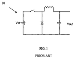
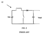
コスト低減は、DC−DC電力コンバータの構成要素を低減すること、例えば、変圧器なしのDC−DCコンバータを提供することによって部分的に達成される。最も一般的な無変圧器dc/dcコンバータのうちの2つは、図1に示すような電圧を下げるためのバックコンバータ10、及び図2に示すような電圧を上げるためのブーストコンバータ12である。
Cost reduction is achieved in part by reducing the components of the DC-DC power converter, for example by providing a DC-DC converter without a transformer. Two of the most common transformerless dc / dc converters are a
入力対出力電圧比が1に近い場合には、これらの回路の両方は、非常に高い変換効率を得ることができるが、これらの効率は、電圧比が高くなった場合は最適とは言えない。効率の損失は、他の作動的問題と共に、ダイオード順電圧の降下、スイッチ及びダイオードの導通損失、スイッチング損失、スイッチのキャパシタンス、誘導子巻線のキャパシタンス、及びリード及びトレースのインダクタンスのような回路効果を含む回路の寄生要素によって引き起こされる。 Both of these circuits can achieve very high conversion efficiencies when the input to output voltage ratio is close to 1, but these efficiencies are not optimal when the voltage ratio increases. . Efficiency losses, along with other operational issues, include circuit effects such as diode forward voltage drop, switch and diode conduction losses, switching losses, switch capacitance, inductor winding capacitance, and lead and trace inductance. Caused by circuit parasitic elements.
更に、特にブーストコンバータは、寄生作用影響を受け易く、高効率の作動が低い昇圧比、例えば、1:2又は1:3を必要とすることは従来技術で公知である。1:10又はそれよりも大きい範囲のような高い昇圧比は、例えば、N.Mohan、T.Undeland、W.Robbins著「電力電子工学:コンバータ、用途、及び設計(Power electronics:converters,applications,and design)」、Wiley、1995年に説明されているように、コスト及び効率の制約条件を踏まえると全く非実用的である。 Furthermore, it is known in the prior art that especially boost converters are susceptible to parasitic effects and high efficiency operation requires a low step-up ratio, eg 1: 2 or 1: 3. A high step-up ratio, such as a range of 1:10 or greater, is, for example, N.I. Mohan, T .; Underland, W.M. As described in Robbins, “Power Electronics: Converters, Applications, and Designs”, Wiley, 1995, totally impractical given cost and efficiency constraints Is.
B.Buti、P.Bartal、I.Nagy著「共振周波数よりも上で作動する共振ブーストコンバータ(Resonant boost converter operating above its resonant frequency)」、EPE、ドレスデン、2005年は、共振DC−DC電力コンバータの例であり、共振タンクがその共振周波数で励起され、変圧器を用いずに高い昇圧/降圧変換比が得られる。Hブリッジベースの共振DC−DC電力コンバータは、(D.Jovcic著「MWサイズ用途のための昇圧MWdc−dcコンバータ(Step−up MW dc−dc converter for MW size applications)」、Institute of Engineering Technology、論文IET−2009−407)によって提案されており、かつ拡張モジュール性に向けてA.Abbas及びP.Lehnによって修正されている(A.Abbas、P.Lehn著「dcからdcへの高電圧コンバータのための電力電子回路(Power electronic circuits for high voltage dc to dc converters)」、トロント大学、発明開示RIS#10001913、2009−03−31)。 B. Buti, P.A. Bartal, I.D. Nagy, “Resonant boost converter operating resonant frequency”, EPE, Dresden, 2005, is an example of a resonant DC-DC power converter. Excited at a frequency, a high step-up / step-down conversion ratio can be obtained without using a transformer. H-bridge based resonant DC-DC power converters are described by D. Jovic, “Step-up MW dc-dc converter for MW size applications,” Institute of Engineering, MW size applications. The paper IET-2009-407) and A. Abbas and P.A. Modified by Lehn (A. Abbas, P. Lehn, "Power electronic circuits for high voltage converter dc to dc converters", University of Toronto, invention disclosure RIS # 10001913, 2009-03-31).
これらの従来技術のトポロジーにはいくつかの欠点がある。 These prior art topologies have several drawbacks.
B.Buti、P.Bartal、I.Nagy著「共振周波数よりも上で作動する共振ブーストコンバータ(Resonant boost converter operating above its resonant frequency)」、EPE、ドレスデン、2005年に開示されているコンバータは、正しく機能するのに、各々が半分の時間しか利用しない2つの完全又はほぼ完全に整合する誘導子を必要とする。完全な整合は、多くの用途において実施不能である。更に、誘導子が半分の時間しか利用しないということにより、回路の誘導要件が実質的に2倍になる。一般的に誘導子は、電力回路内で飛び抜けて最も高価な構成要素であるので、これは望ましくない。更に、B.Buti、P.Bartal、I.Nagy著「共振周波数よりも上で作動する共振ブーストコンバータ(Resonant boost converter operating above its resonant frequency)」、EPE、ドレスデン、2005年は、正と負の両方の入力供給を必要とする。多くの場合にこの入力供給は利用不能である。 B. Buti, P.A. Bartal, I.D. Nagy's "Resonant boost converter operating resonant frequency" converters disclosed in EPE, Dresden, 2005 are each half functioning correctly. Requires two fully or nearly perfectly matched inductors that only use time. Perfect alignment is not feasible in many applications. In addition, the fact that the inductors only use half the time substantially doubles the circuit's inductive requirements. This is undesirable because the inductor is typically the most expensive component by far in the power circuit. Furthermore, B.I. Buti, P.A. Bartal, I.D. Nagy "Resonant boost converter operating resonant frequency", EPE, Dresden, 2005, requires both positive and negative input supplies. In many cases this input supply is not available.
D.Jovcic著「MWサイズ用途のための昇圧MWdc−dcコンバータ(Step−up MW dc−dc converter for MW size applications)」、Institute of Engineering Technology、論文IET−2009−407、及びA.Abbas、P.Lehn著「dcからdcへの高電圧コンバータのための電力電子回路(Power electronic circuits for high voltage dc to dc converters)」、トロント大学、発明開示RIS#10001913、2009−03−31に開示されているコンバータは、4つの高電圧逆阻止スイッチングデバイスを使用する。中程度の周波数の用途(約20kHz〜100kHz)では、そのようなデバイスは容易に利用可能ではなく、従って、これらのデバイスは、絶縁ゲートバイポーラトランジスタ(IGBT)とダイオード、又はMOSFETとダイオードの直列組合せから作成する必要がある。それによってシステムコストが更に増大するだけでなく、コンバータのデバイス導通損失もほぼ2倍になる。 D. Jovic, “Step-up MW dc-dc converter for MW size applications”, Institute of Engineering Technology, Paper IET. Abbas, P.A. Lehn, “Power electronic circuits for high voltage dc to dc converters”, University of Toronto, invention disclosure RIS # 10001913, 2009-03-31. The converter uses four high voltage reverse blocking switching devices. For medium frequency applications (approximately 20-100 kHz), such devices are not readily available and therefore these devices are insulated gate bipolar transistors (IGBTs) and diodes or MOSFETs and diodes in series. Need to create from. This not only further increases system cost, but also nearly doubles the device conduction loss of the converter.
一態様では、本発明は、高い昇圧比のための共振dc−dcコンバータであり、高い昇圧比のための共振dc−dcコンバータは、低電圧フルブリッジ又はハーフブリッジdc−acコンバータと、共振タンクと、高電圧ac−dc整流器と、スイッチの両端の高電圧を維持することによって共振タンク内の電流を中断させるように作動可能である共振タンク内の高電圧制御可能スイッチとを含むことを特徴とする。 In one aspect, the present invention is a resonant dc-dc converter for a high boost ratio, the resonant dc-dc converter for a high boost ratio comprising a low voltage full bridge or half bridge dc-ac converter and a resonant tank. And a high voltage ac-dc rectifier and a high voltage controllable switch in the resonant tank operable to interrupt the current in the resonant tank by maintaining a high voltage across the switch. And
別の態様では、本発明は、高い昇圧比のための共振dc−dcコンバータであり、高い昇圧比のための共振dc−dcコンバータは、低電圧dc−acコンバータと、共振タンクと、高電圧ac−dcコンバータと、以下のもの、すなわち、変圧器を用いない入力及び出力上の共通接地、及び共振タンク内の単一の高電圧制御可能スイッチのうちの1つ又はそれよりも多くとを含むことを特徴とする。 In another aspect, the invention is a resonant dc-dc converter for a high boost ratio, the resonant dc-dc converter for a high boost ratio comprising a low voltage dc-ac converter, a resonant tank, a high voltage an ac-dc converter and one or more of the following: common ground on the input and output without the transformer, and a single high voltage controllable switch in the resonant tank It is characterized by including.
更に別の態様では、本発明は、高い昇圧比のための共振dc−dcコンバータであり、高い昇圧比のための共振dc−dcコンバータは、低電圧dc−acコンバータと、共振タンクと、高電圧ac−dcコンバータと、共振タンク回路内の高電圧制御可能スイッチとを含むことを特徴とし、高い昇圧比のための共振dc−dcコンバータは、以下のもの、すなわち、(i)入力及び出力に対する共通接地平面、及び(ii)入力及び出力間の変圧器のうちの1つ又はそれよりも多くを提供するように作動可能である。 In yet another aspect, the invention is a resonant dc-dc converter for a high boost ratio, the resonant dc-dc converter for a high boost ratio comprising a low voltage dc-ac converter, a resonant tank, A resonant dc-dc converter for high step-up ratio is characterized in that it includes a voltage ac-dc converter and a high voltage controllable switch in a resonant tank circuit: (i) input and output And (ii) is operable to provide one or more of the transformer between the input and output.
更に別の態様では、本発明は、高い昇圧比のための共振dc−dcコンバータであり、高い昇圧比のための共振dc−dcコンバータは、低電圧dc−acコンバータと、共振タンクと、高電圧ac−dcコンバータと、共振タンクの回路内の高電圧制御可能スイッチと、変圧器の使用を必要としない入力及び出力に対する共通接地平面とを含むことを特徴とする。 In yet another aspect, the invention is a resonant dc-dc converter for a high boost ratio, the resonant dc-dc converter for a high boost ratio comprising a low voltage dc-ac converter, a resonant tank, It includes a voltage ac-dc converter, a high voltage controllable switch in the circuit of the resonant tank, and a common ground plane for inputs and outputs that does not require the use of a transformer.
別の態様では、本発明は、共振DC−DCコンバータであり、共振DC−DCコンバータは、高い入力対出力電圧変換を提供するように作動可能である無変圧器DC−DCコンバータ回路を含むことを特徴とし、無変圧器DC−DCコンバータ回路は、低電圧側のフルブリッジコンバータと、高電圧側の半波整流器と、入力及び出力の両方に対して共通である接地とを含む。 In another aspect, the present invention is a resonant DC-DC converter, the resonant DC-DC converter including a transformerless DC-DC converter circuit operable to provide high input to output voltage conversion. The transformerless DC-DC converter circuit includes a low-voltage side full-bridge converter, a high-voltage side half-wave rectifier, and a ground that is common to both input and output.
更に別の態様では、本発明は、変圧器を有するDC−DCコンバータであり、変圧器を有するDC−DCコンバータは、共振タンクと、逆阻止なしの高電圧スイッチの両端の高電圧スイッチを維持することによって共振の高電圧阻止を実施するように変圧器を有するDC−DCコンバータの回路と共に作動可能である高電圧スイッチと、低電圧側のフルブリッジコンバータと、高電圧側の出力整流器とを含むことを特徴とする。 In yet another aspect, the invention is a DC-DC converter having a transformer that maintains a resonant tank and a high voltage switch across the high voltage switch without reverse blocking. A high voltage switch operable with a circuit of a DC-DC converter having a transformer to implement high voltage blocking of resonance, a full bridge converter on the low voltage side, and an output rectifier on the high voltage side. It is characterized by including.
別の態様では、本発明は、バイポーラ出力を供給する変圧器を有する共振DC−DC昇圧コンバータであり、DC−DC昇圧コンバータは、変圧器上の高電圧巻線と、以下のもの、すなわち、電流を正の出力電圧端子に供給するように作動可能な第1の半波整流器及び負の出力電圧端子から電流を引き出すように作動可能な第2の半波整流器を含む2つの半波整流器とを含むことを特徴とする。 In another aspect, the present invention is a resonant DC-DC boost converter having a transformer providing a bipolar output, the DC-DC boost converter comprising a high voltage winding on the transformer and the following: Two half-wave rectifiers including a first half-wave rectifier operable to supply current to the positive output voltage terminal and a second half-wave rectifier operable to draw current from the negative output voltage terminal; It is characterized by including.
更に別の態様では、本発明は、(a)低電圧dc−acコンバータと、(b)共振タンクと、(c)高電圧ac−dcコンバータと、(d)共振タンク内の単一の高電圧制御可能スイッチとを含む高昇圧比に対して備えられた共振dc−dcコンバータである。本発明の実施形態では、単一の高電圧電圧制御可能スイッチは、同調して作動する2つの並列MOSFET又は直列MOSFETとすることができる。 In yet another aspect, the present invention provides (a) a low voltage dc-ac converter, (b) a resonant tank, (c) a high voltage ac-dc converter, and (d) a single high voltage in the resonant tank. A resonant dc-dc converter provided for a high step-up ratio including a voltage controllable switch. In embodiments of the present invention, a single high voltage voltage controllable switch may be two parallel MOSFETs or series MOSFETs that operate in tune.
コンバータ回路は、変圧器を用いずに実施することができる。変圧器は、望ましい場合に及び/又はシステム要件に従って含めることができる。例えば、電気絶縁の必要性は、変圧器の使用によって対処することができると考えられる。 The converter circuit can be implemented without using a transformer. A transformer may be included if desired and / or according to system requirements. For example, the need for electrical insulation could be addressed through the use of transformers.
別の態様では、本発明は、(a)低電圧側のフルブリッジdc−acコンバータと、(b)高電圧側のハーフブリッジac−dcコンバータと、(c)入力及び出力の両方に共通である接地とを含む変圧器なしのDC−DCコンバータ回路を含む共振DC−DCコンバータであり、コンバータ回路は、高い入力対出力電圧変換を提供するように作動可能である。 In another aspect, the invention is common to both (a) a low-voltage side full-bridge dc-ac converter, (b) a high-voltage side half-bridge ac-dc converter, and (c) both input and output. A resonant DC-DC converter including a transformerless DC-DC converter circuit including some ground, the converter circuit being operable to provide high input-to-output voltage conversion.
本発明の更に別の態様では、(a)低電圧側のフルブリッジ又はハーフブリッジdc−acコンバータと、(b)高電圧側のac−dc整流器と、(c)共振タンクと、(d)主共振タンク電流を中断させる高電圧スイッチとを含む変圧器を有するDC−DCコンバータ回路を含む共振DC−DCコンバータ回路を提供し、コンバータ回路は、高電圧スイッチが、逆阻止スイッチを用いて又は用いずに高電圧スイッチの両端で高電圧を維持することによって高電圧阻止を実施することを可能にするように作動可能である。 In yet another aspect of the invention, (a) a low-voltage side full-bridge or half-bridge dc-ac converter, (b) a high-voltage side ac-dc rectifier, (c) a resonant tank, (d) A resonant DC-DC converter circuit is provided that includes a DC-DC converter circuit having a transformer that includes a high voltage switch that interrupts the main resonant tank current, the converter circuit using a reverse blocking switch or It is operable to allow high voltage blocking to be implemented by maintaining a high voltage across the high voltage switch without using it.
この点に関して、本発明の少なくとも1つの実施形態を詳細に説明する前に、本発明は、その用途において以下に続く説明に開示するか又は図面に例示する構成の詳細及び構成要素の配列に限定されないことは理解されるものとする。本発明は、他の実施形態が可能であり、かつ様々な方法で実施及び実行することができる。また、本明細書に使用する表現及び用語は説明目的のものであり、限定的なものと見なすべきではないことは理解されるものとする。 In this regard, before describing at least one embodiment of the invention in detail, the invention is limited in its application to the details of construction and the arrangement of components disclosed in the following description or illustrated in the drawings. It will be understood that this is not done. The invention is capable of other embodiments and of being practiced and carried out in various ways. It is also to be understood that the expressions and terms used herein are for illustrative purposes and should not be considered limiting.
以下に続く本発明の詳細説明を吟味することにより、本発明は、より明快に理解され、本発明の目的が明らかになるであろう。そのような説明は、添付図面を参照する。 By examining the detailed description of the invention that follows, the invention will be understood more clearly and the objects of the invention will become apparent. Such description refers to the accompanying drawings.
図面には本発明の実施形態を一例として示している。本明細書及び図面は、例示目的のもの及び理解を助けるものでしかなく、本発明の制限の定義を意図したものではないことは明確に理解されるものとする。 The drawings show an embodiment of the present invention as an example. It should be clearly understood that the specification and drawings are for illustrative purposes only and aid in understanding and are not intended to define the limitations of the invention.
本発明は、高い入力対出力電圧変換を提供するように作動可能な共振コンバータ回路設計である。特に、本発明は、高い入力対出力電圧変換を可能にし、高い効率の作動を提供する一連のコンバータ回路トポロジーを含むことができる。コンバータ回路トポロジーは、共振タンクと、タンク電流を中断させて、電力伝達量に対する制御を提供しながらゼロ電流及び/又はゼロ電圧スイッチングが提供されるほぼゼロ損失の「保持」状態をもたらすための手段とを含むことができる。特に、これらのコンバータ回路トポロジーは、ほぼゼロ損失の「保持」の持続時間を制御することによってエネルギ伝達を制御することができる。このエネルギ電力伝達制御は、単一の高電圧制御可能スイッチを用いて達成することができる。 The present invention is a resonant converter circuit design operable to provide high input to output voltage conversion. In particular, the present invention can include a series of converter circuit topologies that allow high input to output voltage conversion and provide high efficiency operation. The converter circuit topology interrupts the tank current and provides a means to provide a "hold" state with near zero loss where zero current and / or zero voltage switching is provided while providing control over power transfer Can be included. In particular, these converter circuit topologies can control energy transfer by controlling the duration of “hold” with approximately zero loss. This energy power transfer control can be achieved using a single high voltage controllable switch.
本発明は、低電力作動中の不要な循環電流を回避することができ、それによってタンク構成要素及び低電圧DC/ACコンバータ内の損失を低減し、更に低電圧DC/ACコンバータのゼロ電圧スイッチング及び低電圧DC/ACコンバータのゼロ電流スイッチングに基づいてスイッチング損失を低減する。また、タンク内の高電圧制御可能スイッチのゼロ電流スイッチングを提供することができ、それによってこのスイッチ自体のスイッチング損失を低く保つことができる。 The present invention can avoid unnecessary circulating current during low power operation, thereby reducing losses in the tank components and the low voltage DC / AC converter, and further zero voltage switching of the low voltage DC / AC converter. And reducing switching losses based on zero current switching of low voltage DC / AC converters. Also, zero current switching of the high voltage controllable switch in the tank can be provided, thereby keeping the switching loss of the switch itself low.
本明細書に説明するように、本発明は、高い入力対出力電圧変換を可能にし、高い効率の作動を提供するコンバータ回路トポロジーを呈示するいくつかの実施形態を有することができる。本明細書では、これらの実施形態の例を開示するが、当業者は、これらの例が本発明の範囲を限定することはなく、本発明の他の実施形態も可能であることを認識するであろう。 As described herein, the present invention can have several embodiments that present converter circuit topologies that enable high input-to-output voltage conversion and provide high efficiency operation. Although examples of these embodiments are disclosed herein, those skilled in the art will recognize that these examples do not limit the scope of the invention and that other embodiments of the invention are possible. Will.
明瞭化のために、本発明の開示では「低電圧」という用語を入力定格電圧と同等の定格電圧を有する成分を指すために用い、「高電圧」という用語を共振タンクコンデンサーの両端に見られるピーク電圧レベルと同等又はそれよりも大きい定格電圧を有する成分を指すために使用する。 For clarity, the present disclosure uses the term “low voltage” to refer to a component having a rated voltage equivalent to the input rated voltage, and the term “high voltage” is found across the resonant tank capacitor. Used to refer to a component having a rated voltage equal to or greater than the peak voltage level.
本発明の実施形態では、ほぼゼロ損失の保持状態の適切な実施は、ゼロ電圧スイッチング又はゼロ電流スイッチングを回路内の全ての制御可能なスイッチに対して達成させることができる。 In embodiments of the present invention, proper implementation of the near zero loss hold state can achieve zero voltage switching or zero current switching for all controllable switches in the circuit.
本発明の実施形態は、高い入力対出力電圧変換比のコンバータに対して低い損失のコンバータ回路を提供することができる。 Embodiments of the present invention can provide a low loss converter circuit for high input to output voltage conversion ratio converters.
本発明の回路設計は、様々な要素を含むことができる。一実施形態では、これらの要素は、(1)入力DC/ACコンバータ、(2)共振タンク、(3)タンク中断手段(本明細書に説明するスイッチ等)、及び(4)出力整流器を含むことができる。出力整流器は、例えば、出力ダイオード内の電流増大率を制限するフィルタ誘導子を含むことができる。入力DC/ACに関しては、当業者は、例えば、ハーフブリッジ型又はフルブリッジ型のインバータのようないくつかの異なる種類のインバータを適切なものとすることができることを認識するであろう。更に、当業者は、出力整流器が、例えば、ハーフブリッジ整流器又はフルブリッジ整流器のようないずれかの出力整流器段を含むことができることを認識するであろう。本発明の一部の実施形態では、回路内で出力整流段の前に変圧器を含めることができる。 The circuit design of the present invention can include various elements. In one embodiment, these elements include (1) an input DC / AC converter, (2) a resonant tank, (3) a tank interrupting means (such as a switch described herein), and (4) an output rectifier. be able to. The output rectifier can include, for example, a filter inductor that limits the rate of current increase in the output diode. With respect to input DC / AC, those skilled in the art will recognize that several different types of inverters may be appropriate, such as, for example, half-bridge or full-bridge inverters. Furthermore, those skilled in the art will recognize that the output rectifier can include any output rectifier stage, such as, for example, a half-bridge rectifier or a full-bridge rectifier. In some embodiments of the invention, a transformer may be included in the circuit before the output rectification stage.
本発明の一実施形態では、回路設計は、(1)フルブリッジDC/ACコンバータ、(2)2つのL構成要素及び1つのC構成要素から構成される共振タンク、(3)タンク中断スイッチ、及び(4)出力整流器段(フルブリッジ又はハーフブリッジ)を含む回路とすることができ、入力電圧と出力電圧の両方に対して共通である接地を設けることができる。回路は、変圧器を含んでも含まなくてもよい。フルブリッジ出力整流器が利用される本発明の実施形態では、変圧器を必要とする場合もある。変圧器を含む本発明の実施形態では、共振L構成要素を変圧器設計の中に統合することができる。そのような回路設計を含む本発明の可能な実施形態を図5aから図5dに示している。 In one embodiment of the present invention, the circuit design comprises (1) a full bridge DC / AC converter, (2) a resonant tank composed of two L components and one C component, (3) a tank break switch, And (4) a circuit including an output rectifier stage (full bridge or half bridge), and a ground that is common to both the input voltage and the output voltage can be provided. The circuit may or may not include a transformer. In embodiments of the invention where a full bridge output rectifier is utilized, a transformer may be required. In embodiments of the invention that include a transformer, the resonant L component can be integrated into the transformer design. A possible embodiment of the present invention including such a circuit design is shown in FIGS. 5a to 5d.
本明細書に説明するように、当業者は、本発明の実施形態が変圧器を含むことができ、又は無変圧器のものとすることができることを認識するであろう。本発明の実施形態内に変圧器を含めるという選択は、本発明の実施形態の回路仕様、又は他の優先度又は考察に基づくとすることができる。本明細書は、変圧器要素を含む本発明の実施形態と、変圧器要素を含まない、従って、無変圧器のものである本発明の実施形態との両方の一部の例を開示して説明する。 As described herein, one of ordinary skill in the art will recognize that embodiments of the present invention can include a transformer or can be transformerless. The choice of including a transformer within an embodiment of the present invention may be based on the circuit specifications of the embodiments of the present invention, or other priorities or considerations. This specification discloses some examples of both embodiments of the present invention that include a transformer element and embodiments of the present invention that do not include a transformer element and therefore are transformerless. explain.
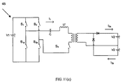
図11a、図11b、及び図11cは、付加的な巻線が主誘導子の磁気コアに追加され、従って、スイッチSxに対する電圧ストレスを低下させる代替的な実施を含む回路42、44、及び46それぞれである本発明の実施形態を示している。巻線の追加は、誘導子Lを絶縁された変圧器に変換することができ、それによって付加的な回路実施の選択肢が与えられる。図11cに示す本発明の実施形態は、バイポーラ出力を供給することができ、それによって電圧をレベルV2の接地に維持しながら2×V2の差動出力を得ることが可能になる。
FIGS. 11a, 11b, and 11c show that
図12に示すように、回路48は、図11cに示す回路の1つの実際的な実施とすることができる。変圧器の励磁分岐は、主共振タンクインダクタンス「L」を与えることができる。適切な変圧器設計により、フィルタインダクタンス「Lf」を変圧器内に統合することができる。この統合は、変圧器を値「Lf」の漏れインダクタンスを有するように設計することによって行うことができる。図12に示すように、全てのスイッチは、MOSFETを用いて実施することができる。導通期間の終了時点における高電圧MOSFETの両端の過渡電圧を制限するために、スナバ回路を使用することができる。電圧V2が高電圧MOSFETの定格電圧よりも低い場合には、スナバは、MOSFETのドレインから正の出力V2への単一のダイオードで構成することができる。それによって通常スナバ回路内で失われるエネルギを出力に伝達することを可能にすることができ、それによってほぼ無損失のスナバがもたらされる。それによって全体的なコンバータ効率を改善することができる。
As shown in FIG. 12,
図13に示すように、本発明の実施形態は、図12のコンバータに対するゲート信号を重要な電圧及び電流の波形と共に含む特定の結果50を生成することができる。以下は、可能なスイッチングサイクル方法の説明である。
1.時間0.900msにおいて、スイッチS1、S2p、及びSxの導通によってサイクルを始めることができる。その後に、正の電圧Vin及び正のタンク入力電流I1によって見られるように、エネルギを共振タンク内に伝達することができる。
2.タンク電流I1がゼロに達すると、スイッチS及びS2pを遮断することができ、その殆ど直後にスイッチS2及びS1pを導通させることができる。それによって電流が負になると同時に入力電圧の極性を負にすることができる。
3.S1及びS20と同時にスイッチSxを遮断することができるが、MOSFET寄生ダイオードは、負の電流の導通を可能にすることができる。MOSFET導通チャンネル内の損失が寄生ダイオードの導通損失よりも低いと計算される場合には、導通損失を低減するためにMOSFETを負の電流パルスの持続時間にわたって導通状態に保たなければならない。
4.電流がゼロに達すると、スイッチSxを遮断すべきである。それによってタンク電流を中断させることができ、回路が、コンバータ作動が休止されてほぼ無損失状態に保持されるほぼゼロ損失の「保持状態」に入ることを可能にすることができる。
5.入力から出力への平均電力伝達量を制御するために、保持状態の持続時間を変更することができる。保持状態に続いて、別の類似の作動サイクルを続けることができる。
As shown in FIG. 13, embodiments of the present invention can produce a
1. At time 0.900 ms, the cycle can begin with the conduction of switches S1, S2p and Sx. Subsequently, energy can be transferred into the resonant tank as seen by the positive voltage Vin and the positive tank input current I1.
2. When the tank current I1 reaches zero, the switches S and S2p can be cut off, and the switches S2 and S1p can be turned on almost immediately thereafter. Thereby, the polarity of the input voltage can be made negative at the same time as the current becomes negative.
3. Although the switch Sx can be shut off simultaneously with S1 and S20, the MOSFET parasitic diode can allow conduction of negative current. If the loss in the MOSFET conduction channel is calculated to be lower than the conduction loss of the parasitic diode, the MOSFET must be kept conducting for the duration of the negative current pulse to reduce conduction loss.
4). When the current reaches zero, switch Sx should be cut off. The tank current can thereby be interrupted and the circuit can be allowed to enter a “zero hold” “holding state” where converter operation is paused and held in a nearly lossless state.
5. In order to control the average power transfer from input to output, the duration of the hold state can be changed. Following the hold state, another similar operating cycle can continue.
共振タンクから出力への電力伝達は、正のdc出力に対して一度、負のdc出力に対して一度、期間毎に2度発生させることができる。正の出力に対する電力伝達は、スイッチS1及びS2pの導通の直後に発生させることができる。負の出力に対する電力伝達は、スイッチS1及びS1pの導通の直後に発生させることができる。 Power transfer from the resonant tank to the output can occur twice per period once for the positive dc output and once for the negative dc output. Power transfer for the positive output can occur immediately after the conduction of switches S1 and S2p. Power transfer to the negative output can occur immediately after conduction of switches S1 and S1p.
本発明の一実施形態では、DC−ACコンバータに回路に単一の制御可能高電圧スイッチを有する(並列)共振タンクが続き、それにAC−DCコンバータが続く構成の回路を提供することができる。 In one embodiment of the present invention, a circuit can be provided that is configured with a DC-AC converter followed by a (parallel) resonant tank with a single controllable high voltage switch followed by an AC-DC converter.
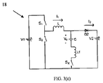
提案する「ハーフブリッジ浮遊タンク」共振DC−DCコンバータ構成を含む本発明の実施形態を図3a、図3b、及び図3cに3つの特定の代表的な実施に示している。図3aに示す本発明の実施形態は、出力フィルタ誘導子を含まない回路14とすることができる。図3aは、本発明の基本的な回路設計の概念を示しており、本発明によるハーフブリッジ浮遊タンクコンバータを提供している。図3bに示す本発明の実施形態は、出力フィルタ誘導子を含む回路16とすることができる。本発明の殆どの実施では、フィルタ誘導子を含むことは実際的な要件である。一般的には、フィルタ誘導子を追加するのに好ましい2つの場所が存在する。第1のものを図3bに例示している。第2のものを図3cに示しており、この図は、タンク内に統合されたフィルタ誘導子を含む回路18とすることができる本発明の実施形態を示している。
Embodiments of the present invention including the proposed “half-bridge floating tank” resonant DC-DC converter configuration are shown in three specific exemplary implementations in FIGS. 3a, 3b, and 3c. The embodiment of the invention shown in FIG. 3a may be a
図4に示すように、本発明の一実施形態では、回路20は、図3a、図3b、及び図3cに示す回路設計の「フルブリッジ浮遊タンク」構成とすることができる。図4は、図3a、図3b、及び図3cに示すコンバータの拡張とすることができる。当業者は、図4に示す回路20が、図5a、図5b、図5c、及び図5dにそれぞれ示す回路22、24、及び26と比較して、例えば、入力及び出力上の共通接地を欠く可能性があり、従って、多くの無変圧器用途に対して望ましくないものである可能性があることを認識するであろう。本発明の実施形態では、入力及び出力の両方の電圧供給源の接地を可能にするために、コンデンサーとダイオード整流器の間に絶縁変圧器を追加することができる。
As shown in FIG. 4, in one embodiment of the present invention,
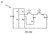
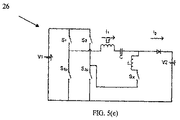
図5a、図5b、図5c、及び図5dに示す本発明の実施形態は、本発明のフルブリッジ共振DC−DCコンバータの変形を表すとすることができ、単一の高電圧スイッチ、及び入力及び出力上の共通接地を含むことができる。より具体的には、図5aに示す本発明の実施形態は、誘導子電流を単一の高電圧スイッチ(Sx)によって切り換えることができる回路22とすることができ、図5bに示す本発明の実施形態は、コンデンサー電流を単一の高電圧スイッチ(Sx)によって切り換えることができる回路24とすることができ、図5cに示す本発明の実施形態は、図5aに示す回路22と類似の回路26とすることができ、図5cに示す回路26は、Sxによって切り換えることができる誘導子電流を含むことができ、かつフィルタ誘導子をタンク内に統合することができ、図5dに示す本発明の実施形態は、図5bに示す回路24と類似の回路28とすることができ、図5dに示す回路28は、Sxによって切り換えることができるコンデンサー電流を含むことができ、かつフィルタ誘導子をタンク内に統合することができる。
The embodiments of the present invention shown in FIGS. 5a, 5b, 5c, and 5d may represent a variation of the full bridge resonant DC-DC converter of the present invention, with a single high voltage switch and input And a common ground on the output. More specifically, the embodiment of the present invention shown in FIG. 5a may be a
図5a、図5b、図5c、及び図5dに示す本発明のDC−DCコンバータは、ハーフブリッジ回路の従来技術のフルブリッジ拡張と比較して、有意な非対称度を示す場合があることを理解すべきである。特に、この非対称性は、接地が非対称であること、入力スイッチ構成が非対称であること、及び出力段が非対称であることにおいて示される場合がある。 It is understood that the DC-DC converter of the present invention shown in FIGS. 5a, 5b, 5c, and 5d may exhibit significant asymmetry compared to the prior art full bridge extension of a half bridge circuit. Should. In particular, this asymmetry may be shown in that the ground is asymmetric, the input switch configuration is asymmetric, and the output stage is asymmetric.
当業者は、本発明の他の変形及び実施形態が可能であることを認識するであろう。例えば、本発明の実施形態は、最先端の逆阻止IGBTデバイスを使用することができ、この場合はSxを排除することができるが、S1及びS2の各々は、高電圧逆阻止IGBTで構成する必要がある場合がある。本発明のそのような実施形態は、タンク内と出力回路内とで厳密に同じ電圧波形及び電流波形をもたらすことができる。多くの他の変形が可能である。 Those skilled in the art will recognize that other variations and embodiments of the present invention are possible. For example, embodiments of the present invention can use state-of-the-art reverse blocking IGBT devices, in which case Sx can be eliminated, but each of S1 and S2 comprises a high voltage reverse blocking IGBT There may be a need. Such an embodiment of the present invention can provide exactly the same voltage and current waveforms in the tank and in the output circuit. Many other variations are possible.
本発明の実施形態では、回路設計は、高電圧スイッチが逆阻止のものである必要はなく、従って、例えば、サイリスタ(スイッチング周波数を過度に低い値に制限する)又はMOSFET−ダイオードの直列組合せ/IGBT−ダイオードの直列組合せの代わりに、MOSFET又はIGBTを使用することができるようなものとすることができる。 In an embodiment of the invention, the circuit design does not require that the high voltage switch be reverse-blocking, and thus, for example, a thyristor (which limits the switching frequency to an excessively low value) or a MOSFET-diode series combination / Instead of a series combination of IGBT-diodes, a MOSFET or IGBT can be used.
また、本発明の実施形態では、以下により詳しく説明するように、回路設計は、電気浮遊タンクを使用することができる。 Also, in embodiments of the present invention, the circuit design can use an electric floating tank, as will be described in more detail below.
以下に本発明のある一定の態様をより詳細に説明するが、これらの詳細内容は、本発明の範囲を何らかの形に限定するものとしてではなく、本発明の実施形態の例として読解すべきである。 Certain aspects of the invention are described in more detail below, but these details should not be construed as limiting the scope of the invention in any way, but as examples of embodiments of the invention. is there.
ハーフブリッジ浮遊タンクコンバータ
本発明の実施形態には、ハーフブリッジ浮遊タンクコンバータを含めることができる。本発明のそのような実施形態では、使用されるスイッチの種類及びタンク回路内での高電圧スイッチ(Sx)の場所/向きに基づいて、スイッチング処理を若干変更することができる。本明細書では、本発明の実施形態に対して使用すべき可能なスイッチング処理の説明は、図6に示すようにS1及びS2がMOSFETを用いて実施され、Sxが高電圧IGBTを用いて実施されるトポロジー30を参照して提供する。
Half Bridge Floating Tank Converter Embodiments of the present invention can include a half bridge floating tank converter. In such embodiments of the present invention, the switching process can be modified slightly based on the type of switch used and the location / orientation of the high voltage switch (Sx) in the tank circuit. In this specification, a description of the possible switching process to be used for an embodiment of the present invention is illustrated in FIG. 6 where S1 and S2 are implemented using MOSFETs, and Sx is implemented using high voltage IGBTs. Provided with reference to the
本発明の一実施形態では、図7に示すように、この実施形態の使用波形結果32は、ハーフブリッジ浮遊タンクコンバータに付随する特定の電圧波形及び電流波形を示す場合がある。例えば、コンバータは、誘導子電流が連続的に振動するのではなく、単一の高電圧スイッチSxによって各期間に一度中断されるモードで作動させることができる。
In one embodiment of the present invention, as shown in FIG. 7, the
回路の作動の例は、以下の通りとすることができる。
1.S1及びSxをLC共振振動の1つのサイクルを開始するように始動することができる。IGBT(Sx)の所定の向きに対して、コンデンサー電圧に対する初期条件を約−V2とすることができる。
2.サイクルの半分に対して電流I1を正とすることができ、入力電圧Vinを正とすることができ、エネルギが回路内に伝達される。
3.VcgがV2に達すると、出力ダイオードは導通し、I1を出力に伝達することができ、出力電力伝達が完了する(出力電流の急激な増大率は、出力ダイオード又はタンクコンデンサーのいずれかと直列で配置される付加的な電流変化率制限誘導子の導入によって低減することができる)。
4.入力電流のゼロ交差においてS1を遮断し、S2を導通させることができる。この時点で出力ダイオードを遮断することができ、IGBT逆導通ダイオードを導通させることができる。それによってタンクの振動を継続することが可能になり、それによって次のサイクルへの準備としてコンデンサーが−V2まで再充電される。
5.電流I1が再度正になることを試行する時に、IGBTは、「オフ」状態にすることができ、従って、電流のゼロ交差においてタンクの振動が中断される。
6.次に、新しいエネルギパルスを必要とするまで、回路を「保持状態」にすることができる。
An example of circuit operation may be as follows.
1. S1 and Sx can be started to initiate one cycle of LC resonant oscillation. For a given orientation of IGBT (Sx), the initial condition for the capacitor voltage can be about -V2.
2. The current I1 can be positive for half the cycle, the input voltage Vin can be positive, and energy is transferred into the circuit.
3. When Vcg reaches V2, the output diode becomes conductive and can transmit I1 to the output, completing the output power transfer (the rapid increase in output current is placed in series with either the output diode or the tank capacitor) Can be reduced by the introduction of additional current change rate limiting inductors).
4). S1 can be interrupted and S2 can be conducted at the zero crossing of the input current. At this point, the output diode can be shut off and the IGBT reverse conducting diode can be conducted. This allows the tank to continue to vibrate, thereby recharging the capacitor to -V2 in preparation for the next cycle.
5. When attempting to make the current I1 positive again, the IGBT can be put into an “off” state, so that the tank oscillation is interrupted at the zero crossing of the current.
6). The circuit can then be "held" until a new energy pulse is needed.
共通接地を有するフルブリッジ浮遊タンクコンバータ
本発明の実施形態は、共通接地を有するフルブリッジ浮遊タンクコンバータを含むことができる。本発明のそのような実施形態では、使用されるスイッチの種類及びタンク回路内での高電圧スイッチ(Sx)の場所/向きに基づいて、スイッチング処理を若干変更することができる。共通接地を有するフルブリッジ浮遊タンクコンバータを含む本発明の一実施形態は、図8に示すように、4つのスイッチS1、S1p、S2、及びS2pがMOSFETを用いて実施され、Sxが高電圧IGBTを用いて実施されるトポロジー34を含むことができる。共通接地を有するフルブリッジ浮遊タンクコンバータを含む本発明の実施形態では、導通期間の終了時点における高電圧MOSFETの両端の過渡電圧を制限するために、スナバ回路を使用することができる。スナバは、IGBTのコレクターから出力への単一のダイオードで構成することができる。それによって通常スナバ回路内で失われるエネルギを出力に伝達することを可能にすることができ、それによってほぼ無損失のスナバがもたらされる。本発明のそのような実施形態は、全体的なコンバータ効率を改善することができる。
Full Bridge Floating Tank Converter with Common Ground Embodiments of the present invention can include a full bridge floating tank converter with a common ground. In such embodiments of the present invention, the switching process can be modified slightly based on the type of switch used and the location / orientation of the high voltage switch (Sx) in the tank circuit. One embodiment of the present invention including a full bridge floating tank converter with a common ground is shown in FIG. 8, where four switches S1, S1p, S2 and S2p are implemented using MOSFETs, and Sx is a high voltage IGBT. The
本発明の一実施形態では、図9に示すように、実施形態の使用波形結果36は、共通接地を有するこのフルブリッジ浮遊タンクコンバータに付随する特定の電圧波形及び電流波形を示す場合がある。コンバータは、誘導子電流が連続的に振動するのではなく、単一の高電圧スイッチSxによって各期間に一度中断されるモードで作動させることができる。
In one embodiment of the invention, as shown in FIG. 9, the
回路の作動の例は、以下の通りとすることができる。
1.IGBT(Sx)の所定の向きに対して、S1、S2p、及びSxをLC共振振動の1つのサイクルを開始するように始動することができる。
2.サイクルの半分に対して電流I1を正とすることができ、入力電圧Vinを正とすることができ、エネルギが回路内に伝達される。
3.I1がゼロを交差すると、S1、S2pを遮断することができ、S2及びS1pを導通させることができる。負のI1の間のいずれかの時点でスイッチSxを無損失で遮断することができ、これは、電流が逆並列ダイオード内を流れていることによる。
4.VcgがV2に達すると、電力を出力に伝達し始めることができる。この伝達は、電流12がゼロに減衰するまで継続させることができる。
5.次に、新しいエネルギパルスを必要とするまで、コンデンサー電圧を「保持状態」にすることができる。
An example of circuit operation may be as follows.
1. For a given orientation of IGBT (Sx), S1, S2p, and Sx can be started to initiate one cycle of LC resonant oscillation.
2. The current I1 can be positive for half the cycle, the input voltage Vin can be positive, and energy is transferred into the circuit.
3. When I1 crosses zero, S1 and S2p can be cut off, and S2 and S1p can be made conductive. At any point during the negative I1, the switch Sx can be losslessly shut off because current is flowing in the anti-parallel diode.
4). When Vcg reaches V2, power can begin to be transferred to the output. This transmission can continue until the current 12 decays to zero.
5. The capacitor voltage can then be “held” until a new energy pulse is needed.
共通接地及びシリコンカーバイドデバイスを有するフルブリッジコンバータ
本発明の実施形態は、多くの用途において必要とされるように入力及び出力上の共通接地を維持しながら、変圧器を使用することなく、タンク電流の正と負の両方の半サイクル中にエネルギを伝達するように作動可能である共通接地を有するフルブリッジ浮遊タンクコンバータを含むことができる。この回路内のSxの目的は、ゼロ電流/ゼロ電圧スイッチングを提供しながら、依然として電力伝達量に対する制御を与えることとすることができる。従って、電力伝達量に対する制御を与えると同時に、ほぼゼロのスイッチング損失を得ることができる。
Full Bridge Converter with Common Ground and Silicon Carbide Device Embodiments of the present invention provide tank current without the use of a transformer while maintaining a common ground on the input and output as required in many applications. A full-bridge floating tank converter with a common ground that is operable to transfer energy during both positive and negative half cycles of the power supply can be included. The purpose of Sx in this circuit may be to still provide control over power transfer while providing zero current / zero voltage switching. Therefore, it is possible to obtain almost zero switching loss while giving control to the power transfer amount.
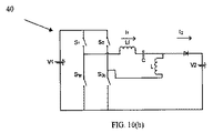
シリコンカーバイドスイッチングデバイスはより費用効果的になるので、最終的にはSxを排除することを価値のあることとすることができる。それにも関わらず、タンク電流の正と負の両方の半サイクル中にエネルギを伝達することができる共通接地構成は、依然として望ましい場合がある。図10a及び図10bの電流トポロジー38及び40は、これを提供するものである。これらのトポロジーは、図5a及び図5cに示す回路設計に関連する場合がある。シリコンカーバイドデバイスは、非常に低いスイッチング損失(特に、ダイオード逆回復電流の除去)をもたらすことができるので、効率に悪影響を及ぼすことなく、ゼロ電流/ゼロ電圧スイッチングを維持する段階を犠牲にすることができる。この場合、電力伝達は、他の共振コンバータにおいて一般的であるように、周波数制御によって達成することができ、R.Erickson、D.Maksimovic著「電力電子工学の基礎(Fundamentals of Power Electronics)」、Kluwer Academic Publishers、2001年を参照されたい。
Since silicon carbide switching devices become more cost effective, it can ultimately be worth eliminating Sx. Nevertheless, a common ground configuration that can transfer energy during both positive and negative half cycles of the tank current may still be desirable. The
R.Erickson、D.Maksimovic著「電力電子工学の基礎(Fundamentals of Power Electronics)」、Kluwer Academic Publishers、2001年に概説されているように、共通接地を有するフルブリッジコンバータは、従来の共振コンバータと比較して重要な利点をもたらすことができる。特に、共通接地を有するフルブリッジコンバータを含む本発明の実施形態のトポロジーは、高い昇圧比と共に入力及び出力における共通接地をもたらすことができ、タンク電流の正と負の両方の半サイクルの間のタンク内への電力伝達をもたらすことができる。 R. Erickson, D.M. As outlined by Maksimovic, “Fundamentals of Power Electronics”, Kluwer Academic Publishers, 2001, a full-bridge converter with a common ground is an important advantage over conventional resonant converters. Can bring. In particular, the topology of an embodiment of the present invention that includes a full bridge converter with a common ground can provide a common ground at the input and output with a high boost ratio, between both positive and negative half cycles of tank current. It can provide power transfer into the tank.
本発明の実施形態の例及びこれらの実施形態がもたらす従来技術に優る利点として、2つの主要な回路配列(ハーフブリッジ浮遊タンクコンバータ、及び共通接地を有するフルブリッジ浮遊タンクコンバータ)の特定の特徴の従来技術に優る利点を以下に説明する。当業者は、以下に解説する特徴及び利点が、一例として提供しているものに過ぎず、他の実施形態及び利点も同様に可能であることを認識するであろう。 Examples of embodiments of the present invention and advantages over the prior art that these embodiments provide include certain features of the two main circuit arrangements (half-bridge floating tank converter and full-bridge floating tank converter with common ground). Advantages over the prior art will be described below. Those skilled in the art will recognize that the features and advantages described below are provided by way of example only, and that other embodiments and advantages are possible as well.
ハーフブリッジ浮遊タンクコンバータ
ハーフブリッジ浮遊タンクコンバータを含む本発明の実施形態は、従来技術に優る特定の利点をもたらすことができる。これらの利点のうちの一部は、以下のものを含む。
1.A.Abbas、P.Lehn著「dcからdcへの高電圧コンバータのための電力電子回路(Power electronic circuits for high voltage dc to dc converters)」、トロント大学、発明開示RIS#10001913、2009−03−31の回路、又はD.Jovcic著「MWサイズ用途のための昇圧MWdc−dcコンバータ(Step−up MW dc−dc converter for MW size applications)」、Institute of Engineering Technology、論文IET−2009−407の回路と比較して、本発明のハーフブリッジ回路は、Sxとラベル付けしている1つの高電圧デバイスしか用いないとすることができる。更に、Sxは、逆阻止デバイスとする必要はない場合がある。
2.本発明の実施形態では、単一の高電圧スイッチは、コンバータの共振作動を中断するように作動可能にすることができ、それによってエネルギ伝達が制御される。
3.本発明の実施形態では、低電圧構成要素のみを用いてS1及びS2を実施することができ、損失が低減する。
4.B.Buti、P.Bartal、I.Nagy著「共振周波数よりも上で作動する共振ブーストコンバータ(Resonant boost converter operating above its resonant frequency)」、EPE、ドレスデン、2005年と比較すると、本発明の実施形態は、単一の電力源及び単一のタンク誘導子しか必要としないとすることができる。
5.本発明の実施形態は、入力AC/DCコンバータのゼロ電流ゼロ電圧スイッチングを可能にすることができる。
Half-Bridge Floating Tank Converter Embodiments of the present invention that include a half-bridge floating tank converter can provide certain advantages over the prior art. Some of these advantages include:
1. A. Abbas, P.A. Lehn "Power electronic circuits for high voltage converter dc to dc converters", University of Toronto, Invention Disclosure RIS # 10001913, 2009-03-31, or D . Jovic, "Step-up MW dc-dc converter for MW size applications", Institute of Engineering Technology, paper IET-200 The half-bridge circuit may use only one high-voltage device labeled Sx. Furthermore, Sx may not need to be a reverse blocking device.
2. In an embodiment of the present invention, a single high voltage switch can be enabled to interrupt the resonant operation of the converter, thereby controlling energy transfer.
3. In embodiments of the present invention, S1 and S2 can be implemented using only low voltage components, reducing losses.
4). B. Buti, P.A. Bartal, I.D. Compared to Nagy “Resonant boost converter operating resonant frequency,” EPE, Dresden, 2005, an embodiment of the present invention is a single power source and a single power source. Only one tank inductor may be required.
5. Embodiments of the present invention can allow zero current zero voltage switching of an input AC / DC converter.
共通接地を有するフルブリッジ浮遊タンクコンバータ
共通接地を有するフルブリッジ浮遊タンクコンバータを含む本発明の実施形態は、従来技術に優る特定の利点をもたらすことができる。これらの利点のうちの一部は、以下のものを含む。
1.A.Abbas、P.Lehn著「dcからdcへの高電圧コンバータのための電力電子回路(Power electronic circuits for high voltage dc to dc converters)」、トロント大学、発明開示RIS#10001913、2009−03−31の回路、又はD.Jovcic著「MWサイズ用途のための昇圧MWdc−dcコンバータ(Step−up MW dc−dc converter for MW size applications)」、Institute of Engineering Technology、論文IET−2009−407の回路と比較して、本発明の実施形態の回路は、図3a、図3b、図3c、及び図3dに示すようにSxとラベル付けしている1つの高電圧デバイスのみを用いて作動させることができる。更に、Sxは、逆阻止デバイスとする必要はない場合がある。
2.P.Lehn著「高い入力対出力電圧変換比のための低スイッチ全数の共振dcdコンバータ(A low switch−count resonant dc/d converter circuit for high input−to−output voltage conversion ratios)」、トロント大学、発明開示RIS#10001968、2009−08−13の回路、又は本発明のハーフブリッジ回路と比較すると、本発明の実施形態のフルブリッジDC−DCコンバータは、タンク電流の正と負の両方の半サイクル中に電力源からタンクにエネルギを伝達することができるので、ほぼ2倍の電力伝達を可能にすることができる。
3.本発明の実施形態は、入力ac/dcコンバータのゼロ電流/ゼロ電圧スイッチングを可能にすることができる。
4.本発明の実施形態では、入力電圧供給源と出力電圧供給源の間に共通接地を設けることができる。
5.本発明の実施形態では、単一の高電圧スイッチは、コンバータの共振作動を中断するように作動可能にすることができ、それによってエネルギ伝達が制御される。
Full Bridge Floating Tank Converter with Common Ground Embodiments of the present invention that include a full bridge floating tank converter with a common ground can provide certain advantages over the prior art. Some of these advantages include:
1. A. Abbas, P.A. Lehn "Power electronic circuits for high voltage converter dc to dc converters", University of Toronto, Invention Disclosure RIS # 10001913, 2009-03-31, or D . Jovic, "Step-up MW dc-dc converter for MW size applications", Institute of Engineering Technology, paper IET-200 The circuit of this embodiment can be operated with only one high voltage device labeled Sx as shown in FIGS. 3a, 3b, 3c, and 3d. Furthermore, Sx may not need to be a reverse blocking device.
2. P. Lehn, “Low switch-count resonant dc / d converter circuit for high input-to-output voltage conversion”, University of Toronto Compared to the circuit of RIS # 10001968, 2009-08-13, or the half-bridge circuit of the present invention, the full-bridge DC-DC converter of the embodiment of the present invention is used during both positive and negative half cycles of the tank current. Since energy can be transferred from the power source to the tank, it is possible to transfer power almost twice as much.
3. Embodiments of the present invention can allow zero current / zero voltage switching of the input ac / dc converter.
4). In an embodiment of the present invention, a common ground can be provided between the input voltage supply source and the output voltage supply source.
5. In an embodiment of the present invention, a single high voltage switch can be enabled to interrupt the resonant operation of the converter, thereby controlling energy transfer.
当業者は、本発明の技術の多くの実施が可能であることを認識するであろう。本発明の実施形態の回路設計は、モジュール構造を提供することができ、従って、上述のような設計の機能を可能にしながら、構成要素を追加又は削除することができる。例えば、本発明のDC−DCコンバータの特定的な実施形態は、無変圧器のものとすることができる。本発明の他の実施形態では、図4に示す回路のような回路内に変圧器を含むことを望ましいとすることができる。例えば、図4に示す回路内の共振タンク誘導子とダイオード整流器の間、又は共振タンクコンデンサーとダイオード整流器の間のいずれかに変圧器を含めることができる。また、本発明の一部の実施形態においてSxの使用を説明したが、この構成要素は、例えば、最先端の逆阻止IGBTデバイスを使用することによって排除することができ、この場合、S1及びS2の各々は、高電圧逆阻止IGBTで構成することが必要になる。 Those skilled in the art will recognize that many implementations of the techniques of the present invention are possible. The circuit design of embodiments of the present invention can provide a modular structure, and thus components can be added or removed while allowing the functionality of the design as described above. For example, a particular embodiment of the DC-DC converter of the present invention can be of a transformerless type. In other embodiments of the present invention, it may be desirable to include a transformer in a circuit such as the circuit shown in FIG. For example, a transformer can be included either between the resonant tank inductor and the diode rectifier in the circuit shown in FIG. 4 or between the resonant tank capacitor and the diode rectifier. Also, although the use of Sx has been described in some embodiments of the present invention, this component can be eliminated, for example, by using a state-of-the-art reverse blocking IGBT device, where S1 and S2 Each of which needs to be composed of a high voltage reverse blocking IGBT.
当業者は、本発明の実施形態において本明細書に説明して図示したトポロジーの特定的な態様は、これらのトポロジーの本質、本質的な要素、及び本質的な機能から逸脱することなく修正することができることを認識するであろう。例えば、図11(b)に示す回路設計42では、LfとCが、いずれの中点も伴わずに直列にある場合に、LfとCを交換することを可能にすることができる。同様に、変圧器との併用時には、同じ目的を実現するために、幾つもの公知の出力巻線及び整流器の構成を適用することができる。
Those skilled in the art will appreciate that the specific aspects of the topologies described and illustrated herein in the embodiments of the present invention can be modified without departing from the nature, essential elements, and essential functions of these topologies. You will recognize that you can. For example, the
本発明の一実施形態では、例えば、図10(b)に示すようなスイッチング要素は、シリコンカーバイドデバイスを使用することができる。スイッチングは、タンク回路への+V1と−V1の間の矩形波電圧スイッチングを可能にするように実施することができる。矩形波電圧を供給するように実施されるスイッチングは、タンク回路への+V1と0の間(又は0と−V1の間)のスイッチングとすることができる。タンク入力電圧スイッチングは、定格電力の近くで作動する時にかつ低電力下で+V1と0の間(又は0と−V1の間)で作動する時に、+V1と−V1の間で発生させることができる。代替的に、この段落に説明している要素は、誘導子Lfが出力経路に移動される(図10aに示すように)トポロジーに対して使用することができる。 In one embodiment of the present invention, for example, a silicon carbide device can be used for the switching element as shown in FIG. The switching can be implemented to allow square wave voltage switching between + V1 and -V1 to the tank circuit. The switching implemented to provide a square wave voltage can be a switching between + V1 and 0 (or between 0 and -V1) to the tank circuit. Tank input voltage switching can occur between + V1 and -V1 when operating near rated power and when operating between + V1 and 0 (or between 0 and -V1) under low power. . Alternatively, the elements described in this paragraph can be used for topologies where the inductor Lf is moved to the output path (as shown in FIG. 10a).
本明細書に説明する実施形態の他の変形を本発明の範囲から逸脱することなく実施することができることは、当業者によって認められるであろう。従って、他の修正も可能である。当業者は、説明したDC−DCコンバータ技術に対して多くの用途が存在することを認識するであろう。本発明のDC−DCコンバータは、高い入力対出力電圧変換を提供する多くの構成要素に対する効率的で廉価な代替を提供することができる。更に、本発明の実施形態である高い増幅比を有するDC−DCコンバータは、再生可能/代替エネルギ用途において固定電圧のDCバスを作成するのに使用することができる。 It will be appreciated by those skilled in the art that other variations of the embodiments described herein can be practiced without departing from the scope of the present invention. Accordingly, other modifications are possible. Those skilled in the art will recognize that there are many applications for the DC-DC converter technology described. The DC-DC converter of the present invention can provide an efficient and inexpensive alternative to many components that provide high input-to-output voltage conversion. Furthermore, DC-DC converters with high amplification ratios that are embodiments of the present invention can be used to create a fixed voltage DC bus in renewable / alternative energy applications.
10 バックコンバータ 10 Buck converter
Claims (19)
(a)低電圧フルブリッジ又はハーフブリッジdc−acコンバータ、
(b)共振タンク、
(c)高電圧ac−dc整流器、及び
(d)スイッチの両端の高電圧を維持することによって前記共振タンク内の電流を中断させるように作動可能である該共振タンク内の高電圧制御可能スイッチ、
を含むことを特徴とする共振dc−dcコンバータ。 A resonant dc-dc converter for high step-up ratio,
(A) Low voltage full bridge or half bridge dc-ac converter,
(B) a resonant tank;
(C) a high voltage ac-dc rectifier, and (d) a high voltage controllable switch in the resonant tank operable to interrupt the current in the resonant tank by maintaining a high voltage across the switch. ,
A resonant dc-dc converter comprising:
(a)高電圧MOSFETである前記高電圧スイッチのドレイン、
(b)IGBTである前記高電圧スイッチのコレクター、又は
(c)サイリスタである前記高電圧スイッチのアノード、
のいずれかからダイオードを高昇圧比のための共振dc−dcコンバータの出力端子に接続することにより、高い昇圧比のための共振dc−dcコンバータに導入されることを特徴とする請求項2に記載の高い昇圧比のための共振dc−dcコンバータ。 Lossless snubber circuit
(A) the drain of the high voltage switch which is a high voltage MOSFET;
(B) a collector of the high voltage switch that is an IGBT; or (c) an anode of the high voltage switch that is a thyristor;
The diode is connected to an output terminal of a resonant dc-dc converter for a high boost ratio from any of the above, and is introduced into a resonant dc-dc converter for a high boost ratio. Resonant dc-dc converter for the described high step-up ratio.
(a)低電圧dc−acコンバータ、
(b)共振タンク、
(c)高電圧ac−dcコンバータ、及び
(d)(i)変圧器を用いない入力及び出力上の共通接地、及び
(ii)前記共振タンク内の単一の高電圧制御可能スイッチ、
のうちの1つ又はそれよりも多く、
を含むことを特徴とする共振dc−dcコンバータ。 A resonant dc-dc converter for high step-up ratio,
(A) a low voltage dc-ac converter;
(B) a resonant tank;
(C) a high voltage ac-dc converter, and (d) (i) a common ground on the input and output without the transformer, and (ii) a single high voltage controllable switch in the resonant tank;
One or more of
A resonant dc-dc converter comprising:
(a)低電圧dc−acコンバータ、
(b)共振タンク、
(c)高電圧ac−dcコンバータ、及び
(d)前記共振タンクの回路内の高電圧制御可能スイッチ、
を含み、
高い昇圧比のための共振dc−dcコンバータが、(i)入力及び出力のための共通接地平面、及び(ii)入力及び出力間の変圧器のうちの1つ又はそれよりも多くを提供するように作動可能である、
ことを特徴とする共振dc−dcコンバータ。 A resonant dc-dc converter for high step-up ratio,
(A) a low voltage dc-ac converter;
(B) a resonant tank;
(C) a high voltage ac-dc converter, and (d) a high voltage controllable switch in the circuit of the resonant tank,
Including
A resonant dc-dc converter for high step-up ratio provides one or more of (i) a common ground plane for input and output, and (ii) a transformer between input and output. Is operable as
A resonant dc-dc converter characterized by the above.
(a)低電圧dc−acコンバータ、
(b)共振タンク、
(c)高電圧ac−dcコンバータ、
(d)前記共振タンクの回路内の高電圧制御可能スイッチ、及び
(e)変圧器の使用を必要としない入力及び出力のための共通接地平面、
を含むことを特徴とする共振dc−dcコンバータ。 A resonant dc-dc converter for high step-up ratio,
(A) a low voltage dc-ac converter;
(B) a resonant tank;
(C) a high voltage ac-dc converter;
(D) a high voltage controllable switch in the circuit of the resonant tank; and (e) a common ground plane for inputs and outputs that does not require the use of a transformer;
A resonant dc-dc converter comprising:
(i)低電圧側のフルブリッジコンバータ、
(ii)高電圧側の半波整流器、及び
(iii)入力及び出力の両方に共通である接地、
を含む無変圧器DC−DCコンバータ回路、
を含むことを特徴とする共振DC−DCコンバータ。 (A) operable to provide high input to output voltage conversion;
(I) a low-voltage side full-bridge converter,
(Ii) a half-wave rectifier on the high voltage side; and (iii) ground common to both input and output;
A transformerless DC-DC converter circuit, including
A resonant DC-DC converter.
(a)共振タンク、
(b)逆阻止なしの高電圧スイッチにわたる高電圧スイッチを維持することによって共振の高電圧阻止を実施するために変圧器を有するDC−DCコンバータの回路と共に作動可能である高電圧スイッチ、
(c)低電圧側のフルブリッジコンバータ、及び
(d)高電圧側の出力整流器、
を含むことを特徴とするDC−DCコンバータ。 A DC-DC converter having a transformer,
(A) a resonant tank;
(B) a high voltage switch operable with a circuit of a DC-DC converter having a transformer to implement high voltage blocking of resonance by maintaining a high voltage switch across the high voltage switch without reverse blocking;
(C) a low voltage side full bridge converter, and (d) a high voltage side output rectifier,
DC-DC converter characterized by including.
(a)変圧器上の高電圧巻線と、
(b)(i)電流を正の出力電圧端子に供給するように作動可能な第1の半波整流器、及び
(ii)負の出力電圧端子から電流を引き出すように作動可能な第2の半波整流器、
を含む2つの半波整流器と、
を含むことを特徴とする共振DC−DC昇圧コンバータ。 A resonant DC-DC boost converter having a transformer for providing a bipolar output,
(A) a high voltage winding on the transformer;
(B) (i) a first half-wave rectifier operable to supply current to the positive output voltage terminal; and (ii) a second half operable to draw current from the negative output voltage terminal. Wave rectifier,
Two half-wave rectifiers including:
A resonant DC-DC boost converter.
Applications Claiming Priority (3)
| Application Number | Priority Date | Filing Date | Title |
|---|---|---|---|
| US30559010P | 2010-02-18 | 2010-02-18 | |
| US61/305,590 | 2010-02-18 | ||
| PCT/CA2011/000185 WO2011100827A1 (en) | 2010-02-18 | 2011-02-18 | Dc-dc converter circuit for high input-to-output voltage conversion |
Publications (1)
| Publication Number | Publication Date |
|---|---|
| JP2013520148A true JP2013520148A (en) | 2013-05-30 |
Family
ID=44482425
Family Applications (1)
| Application Number | Title | Priority Date | Filing Date |
|---|---|---|---|
| JP2012553160A Withdrawn JP2013520148A (en) | 2010-02-18 | 2011-02-18 | DC-DC converter circuit for high input-to-output voltage conversion |
Country Status (11)
| Country | Link |
|---|---|
| US (1) | US9318968B2 (en) |
| EP (1) | EP2537241A1 (en) |
| JP (1) | JP2013520148A (en) |
| KR (1) | KR20130043612A (en) |
| CN (1) | CN102859855B (en) |
| AU (1) | AU2011217688A1 (en) |
| BR (1) | BR112012020845A2 (en) |
| CA (1) | CA2768517C (en) |
| MA (1) | MA34080B1 (en) |
| RU (1) | RU2012140675A (en) |
| WO (1) | WO2011100827A1 (en) |
Cited By (2)
| Publication number | Priority date | Publication date | Assignee | Title |
|---|---|---|---|---|
| WO2017002845A1 (en) * | 2015-06-30 | 2017-01-05 | ダイハツ工業株式会社 | Plasma reactor power supply device |
| JP2017017995A (en) * | 2016-10-12 | 2017-01-19 | ローム株式会社 | Wireless power supply device having high-speed switching operation circuit, and ac/dc power supply circuit |
Families Citing this family (20)
| Publication number | Priority date | Publication date | Assignee | Title |
|---|---|---|---|---|
| US9059636B2 (en) | 2010-02-18 | 2015-06-16 | Peter Waldemar Lehn | DC-DC converter circuit using LLC circuit in the region of voltage gain above unity |
| MA34080B1 (en) | 2010-02-18 | 2013-03-05 | Peter Waldemar Lehn | Constant current transformer Continuous to convert high-pressure inlet and outlet |
| WO2013166579A1 (en) * | 2012-05-10 | 2013-11-14 | Arda Power Inc. | Dc-dc converter circuit using an llc circuit in the region of voltage gain above unity |
| US8648643B2 (en) * | 2012-02-24 | 2014-02-11 | Transphorm Inc. | Semiconductor power modules and devices |
| WO2014032156A1 (en) * | 2012-08-27 | 2014-03-06 | Bombardier Transportation Gmbh | Adaptive soft switching control for power converter |
| JP2015095988A (en) * | 2013-11-13 | 2015-05-18 | 株式会社東芝 | Dc-dc converter |
| WO2015105795A1 (en) * | 2014-01-07 | 2015-07-16 | Arizona Board Of Regents On Behalf Of Arizona State University | Zero-voltage transition in power converters with an auxiliary circuit |
| MX357520B (en) * | 2014-02-27 | 2018-07-12 | Univ Danmarks Tekniske | On and off controlled resonant dc-dc power converter. |
| US9461547B2 (en) * | 2014-03-07 | 2016-10-04 | Cree, Inc. | Converter circuitry |
| US9401708B2 (en) * | 2014-05-20 | 2016-07-26 | General Electric Company | Gate drive unit and method for controlling a gate drive unit |
| US9559602B2 (en) * | 2015-02-26 | 2017-01-31 | Infineon Technologies Austria Ag | Magnetizing current based control of resonant converters |
| CN105634447B (en) * | 2016-01-11 | 2018-10-19 | 天津工业大学 | Generate the energy-saving control circuit in a variety of magnetic fields |
| US10686378B2 (en) * | 2016-12-16 | 2020-06-16 | Futurewei Technologies, Inc. | High-efficiency regulated buck-boost converter |
| US10277140B2 (en) | 2017-08-31 | 2019-04-30 | Google Llc | High-bandwith resonant power converters |
| US10298138B2 (en) | 2017-08-31 | 2019-05-21 | Google Llc | Programmable power adapter |
| CN113890332A (en) * | 2017-09-05 | 2022-01-04 | 莱恩半导体股份有限公司 | Circuit for hybrid switched capacitor converter |
| WO2020000091A1 (en) * | 2018-06-25 | 2020-01-02 | The Governing Council Of The University Of Toronto | Modular multi-level dc/dc converter with current-shaping |
| CN110391747B (en) * | 2019-07-24 | 2020-09-18 | 山东大学 | High step-up ratio isolation DC-DC converter topology and control method thereof |
| CN111682757B (en) * | 2020-05-21 | 2021-11-19 | 西安交通大学 | Non-isolated high-voltage-reduction-gain DC-DC converter |
| CN115985941B (en) * | 2023-03-21 | 2023-06-23 | 上海埃积半导体有限公司 | Longitudinal RC-IGBT structure and preparation method thereof |
Family Cites Families (27)
| Publication number | Priority date | Publication date | Assignee | Title |
|---|---|---|---|---|
| US5027263A (en) * | 1988-09-16 | 1991-06-25 | Kyushu University | Switching power source means |
| JP3164838B2 (en) * | 1991-06-19 | 2001-05-14 | 株式会社日立製作所 | Switching circuit, conversion device using the same, and power factor improving power supply device |
| US5530638A (en) | 1993-09-24 | 1996-06-25 | At&T Corp. | Multi-resonant electronic power converter with a wide dynamic range |
| US5486752A (en) * | 1994-06-17 | 1996-01-23 | Center For Innovative Technology** | Zero-current transition PWM converters |
| JP2730506B2 (en) * | 1995-02-27 | 1998-03-25 | 日本電気株式会社 | DC / DC converter using piezoelectric transformer |
| US5875103A (en) * | 1995-12-22 | 1999-02-23 | Electronic Measurements, Inc. | Full range soft-switching DC-DC converter |
| US5640082A (en) * | 1996-01-31 | 1997-06-17 | Hughes Electronics | Duty cycle controlled switch variable capacitor circuit |
| US5774351A (en) * | 1996-05-21 | 1998-06-30 | National Science Council | Series resonant DC-to-AC inverter system |
| US6016257A (en) | 1996-12-23 | 2000-01-18 | Philips Electronics North America Corporation | Voltage regulated power supply utilizing phase shift control |
| FR2790150B1 (en) * | 1999-02-19 | 2001-06-08 | Ge Medical Syst Sa | METHOD FOR REGULATING A DOUBLE RESONANCE GENERATOR |
| US6370050B1 (en) * | 1999-09-20 | 2002-04-09 | Ut-Batelle, Llc | Isolated and soft-switched power converter |
| US6304461B1 (en) * | 2000-06-15 | 2001-10-16 | Supertex, Inc. | DC power converter having bipolar output and bi-directional reactive current transfer |
| US6344979B1 (en) | 2001-02-09 | 2002-02-05 | Delta Electronics, Inc. | LLC series resonant DC-to-DC converter |
| JP4017490B2 (en) * | 2002-10-02 | 2007-12-05 | 株式会社デンソー | DC / DC converter |
| US6989997B2 (en) * | 2003-06-25 | 2006-01-24 | Virginia Tech Intellectual Properties, Inc. | Quasi-resonant DC-DC converters with reduced body diode loss |
| US6906931B1 (en) * | 2004-01-30 | 2005-06-14 | Astec International Limited | Zero-voltage switching half-bridge DC-DC converter topology by utilizing the transformer leakage inductance trapped energy |
| WO2006119362A2 (en) * | 2005-05-03 | 2006-11-09 | Massachusetts Institute Of Technology | Methods and apparatus for resistance compression networks |
| US20080089103A1 (en) * | 2005-06-13 | 2008-04-17 | Cheng-Chia Hsu | High efficiency dc to ac power converter |
| US20070047275A1 (en) * | 2005-08-30 | 2007-03-01 | Hesterman Bryce L | Bipolar power supply with lossless snubber |
| TW200733523A (en) * | 2005-10-25 | 2007-09-01 | Koninkl Philips Electronics Nv | Power converter |
| US7548435B2 (en) * | 2006-03-31 | 2009-06-16 | Astec International Limited | Zero-voltage-switching DC-DC converters with synchronous rectifiers |
| US7286373B1 (en) * | 2006-04-07 | 2007-10-23 | Li Shin International Enterprise Corporation | Full-resonant power circuit device for receiving a variable input voltage |
| TWI340528B (en) | 2007-04-03 | 2011-04-11 | Delta Electronics Inc | Resonant converter system and controlling method thereof having relatively better efficiency |
| US20090034298A1 (en) * | 2007-07-30 | 2009-02-05 | Champion Microelectronic Corporation | Control Method And Apparatus Of Resonant Type DC/DC Converter With Low Power Loss At Light Load And Standby |
| TWI346440B (en) * | 2008-01-31 | 2011-08-01 | Lite On Technology Corp | Controller for use in resonant direct current/direct current converter |
| ATE545194T1 (en) * | 2008-03-06 | 2012-02-15 | Koninkl Philips Electronics Nv | CONTROL UNIT FOR A DC-AC CONVERTER OF A RESONANT POWER CONVERSION CIRCUIT, IN PARTICULAR FOR A DC-AC CONVERTER FOR USE IN A HIGH VOLTAGE GENERATOR CIRCUIT OF A MODERN COMPUTER TOMOGRAPHY APPARATUS OR AN X-RAY SYSTEM |
| MA34080B1 (en) | 2010-02-18 | 2013-03-05 | Peter Waldemar Lehn | Constant current transformer Continuous to convert high-pressure inlet and outlet |
-
2011
- 2011-02-18 MA MA35236A patent/MA34080B1/en unknown
- 2011-02-18 US US13/384,294 patent/US9318968B2/en active Active
- 2011-02-18 EP EP11744219A patent/EP2537241A1/en not_active Withdrawn
- 2011-02-18 KR KR1020127024170A patent/KR20130043612A/en not_active Application Discontinuation
- 2011-02-18 AU AU2011217688A patent/AU2011217688A1/en not_active Abandoned
- 2011-02-18 CN CN201180017205.5A patent/CN102859855B/en not_active Expired - Fee Related
- 2011-02-18 WO PCT/CA2011/000185 patent/WO2011100827A1/en active Application Filing
- 2011-02-18 CA CA2768517A patent/CA2768517C/en active Active
- 2011-02-18 JP JP2012553160A patent/JP2013520148A/en not_active Withdrawn
- 2011-02-18 RU RU2012140675/07A patent/RU2012140675A/en not_active Application Discontinuation
- 2011-02-18 BR BR112012020845A patent/BR112012020845A2/en not_active IP Right Cessation
Cited By (3)
| Publication number | Priority date | Publication date | Assignee | Title |
|---|---|---|---|---|
| WO2017002845A1 (en) * | 2015-06-30 | 2017-01-05 | ダイハツ工業株式会社 | Plasma reactor power supply device |
| JP2017017851A (en) * | 2015-06-30 | 2017-01-19 | ダイハツ工業株式会社 | Power supply unit for plasma reactor |
| JP2017017995A (en) * | 2016-10-12 | 2017-01-19 | ローム株式会社 | Wireless power supply device having high-speed switching operation circuit, and ac/dc power supply circuit |
Also Published As
| Publication number | Publication date |
|---|---|
| MA34080B1 (en) | 2013-03-05 |
| CA2768517A1 (en) | 2011-08-25 |
| AU2011217688A1 (en) | 2012-10-11 |
| US20120195074A1 (en) | 2012-08-02 |
| US9318968B2 (en) | 2016-04-19 |
| WO2011100827A1 (en) | 2011-08-25 |
| KR20130043612A (en) | 2013-04-30 |
| RU2012140675A (en) | 2014-03-27 |
| CN102859855A (en) | 2013-01-02 |
| BR112012020845A2 (en) | 2016-07-19 |
| CN102859855B (en) | 2016-03-09 |
| EP2537241A1 (en) | 2012-12-26 |
| CA2768517C (en) | 2017-06-20 |
Similar Documents
| Publication | Publication Date | Title |
|---|---|---|
| JP2013520148A (en) | DC-DC converter circuit for high input-to-output voltage conversion | |
| Lei et al. | Nonisolated high step-up soft-switching DC–DC converter with interleaving and Dickson switched-capacitor techniques | |
| EP3058648B1 (en) | Gate drive apparatus for resonant converters | |
| US9065349B2 (en) | Control method for bidirectional DC-DC converters | |
| US8432709B2 (en) | DC-to-AC power inverting apparatus for photovoltaic modules | |
| Gui et al. | A high voltage-gain LLC micro-converter with high efficiency in wide input range for PV applications | |
| EP2571154A2 (en) | PV inverter with input parallel output series connected flyback converters feeding a fullbridge grid converter | |
| CN110176812B (en) | Hybrid control apparatus and method | |
| CN105144561A (en) | DC-DC converter | |
| Wu et al. | Interleaved phase-shift full-bridge converter with transformer winding series–parallel autoregulated (SPAR) current doubler rectifier | |
| Zhang et al. | A ZCS full-bridge converter without voltage overstress on the switches | |
| Zhao et al. | Efficiency improvement of an adaptive-energy-storage full-bridge converter by modifying turns ratio of a coupled inductor | |
| Yin et al. | A ZCS-PWM voltage-driven three-level converter with a secondary-side simple soft-switching snubber | |
| KR100911541B1 (en) | Bi-Directional Tri-State PWM DC To DC Converter For Fuel Cell Vehicle | |
| Shimada et al. | Two novel control methods expanding input-output operating range for a bi-directional isolated DC-DC converter with active clamp circuit | |
| CN114825663A (en) | SP type double-output independently adjustable wireless power transmission system and control method thereof | |
| Yisheng et al. | A parallel front-end LCL resonant push-pull converter with a coupled inductor for automotive applications | |
| He et al. | High step-up active-clamp converter with an input current doubler and a symmetrical switched-capacitor circuit | |
| JP3934654B2 (en) | DC-DC converter | |
| Moradisizkoohi et al. | Ultra-high step-up DC/DC converter based on dual-coupled-inductors with low voltage stress and input current ripple for renewable energy applications | |
| Shimada et al. | A novel scheme for a bi-directional isolated DC-DC converter with a DC-link diode using reverse recovery current | |
| CN114747113A (en) | Charging device and method for operating a charging device | |
| Blinov et al. | Improved modulation method for full-bridge AC-DC HF-link converter | |
| KR100428422B1 (en) | Zero Voltage Switching Fullbridge Converter | |
| KR20160101808A (en) | Full-Bridge DC-DC Converter |
Legal Events
| Date | Code | Title | Description |
|---|---|---|---|
| A300 | Application deemed to be withdrawn because no request for examination was validly filed |
Free format text: JAPANESE INTERMEDIATE CODE: A300 Effective date: 20140513 |