JP2013510376A - Control performance state by tracking probe activity levels - Google Patents
Control performance state by tracking probe activity levels Download PDFInfo
- Publication number
- JP2013510376A JP2013510376A JP2012538025A JP2012538025A JP2013510376A JP 2013510376 A JP2013510376 A JP 2013510376A JP 2012538025 A JP2012538025 A JP 2012538025A JP 2012538025 A JP2012538025 A JP 2012538025A JP 2013510376 A JP2013510376 A JP 2013510376A
- Authority
- JP
- Japan
- Prior art keywords
- probe
- performance state
- probe activity
- activity level
- threshold
- Prior art date
- Legal status (The legal status is an assumption and is not a legal conclusion. Google has not performed a legal analysis and makes no representation as to the accuracy of the status listed.)
- Pending
Links
Images


Classifications
-
- G—PHYSICS
- G06—COMPUTING; CALCULATING OR COUNTING
- G06F—ELECTRIC DIGITAL DATA PROCESSING
- G06F12/00—Accessing, addressing or allocating within memory systems or architectures
- G06F12/02—Addressing or allocation; Relocation
- G06F12/08—Addressing or allocation; Relocation in hierarchically structured memory systems, e.g. virtual memory systems
- G06F12/0802—Addressing of a memory level in which the access to the desired data or data block requires associative addressing means, e.g. caches
- G06F12/0806—Multiuser, multiprocessor or multiprocessing cache systems
- G06F12/0808—Multiuser, multiprocessor or multiprocessing cache systems with cache invalidating means
-
- G—PHYSICS
- G06—COMPUTING; CALCULATING OR COUNTING
- G06F—ELECTRIC DIGITAL DATA PROCESSING
- G06F1/00—Details not covered by groups G06F3/00 - G06F13/00 and G06F21/00
- G06F1/26—Power supply means, e.g. regulation thereof
- G06F1/32—Means for saving power
-
- G—PHYSICS
- G06—COMPUTING; CALCULATING OR COUNTING
- G06F—ELECTRIC DIGITAL DATA PROCESSING
- G06F1/00—Details not covered by groups G06F3/00 - G06F13/00 and G06F21/00
- G06F1/26—Power supply means, e.g. regulation thereof
- G06F1/32—Means for saving power
- G06F1/3203—Power management, i.e. event-based initiation of a power-saving mode
-
- G—PHYSICS
- G06—COMPUTING; CALCULATING OR COUNTING
- G06F—ELECTRIC DIGITAL DATA PROCESSING
- G06F12/00—Accessing, addressing or allocating within memory systems or architectures
- G06F12/02—Addressing or allocation; Relocation
- G06F12/08—Addressing or allocation; Relocation in hierarchically structured memory systems, e.g. virtual memory systems
- G06F12/0802—Addressing of a memory level in which the access to the desired data or data block requires associative addressing means, e.g. caches
- G06F12/0806—Multiuser, multiprocessor or multiprocessing cache systems
- G06F12/0815—Cache consistency protocols
- G06F12/0831—Cache consistency protocols using a bus scheme, e.g. with bus monitoring or watching means
-
- G—PHYSICS
- G06—COMPUTING; CALCULATING OR COUNTING
- G06F—ELECTRIC DIGITAL DATA PROCESSING
- G06F2212/00—Indexing scheme relating to accessing, addressing or allocation within memory systems or architectures
- G06F2212/10—Providing a specific technical effect
- G06F2212/1028—Power efficiency
-
- Y—GENERAL TAGGING OF NEW TECHNOLOGICAL DEVELOPMENTS; GENERAL TAGGING OF CROSS-SECTIONAL TECHNOLOGIES SPANNING OVER SEVERAL SECTIONS OF THE IPC; TECHNICAL SUBJECTS COVERED BY FORMER USPC CROSS-REFERENCE ART COLLECTIONS [XRACs] AND DIGESTS
- Y02—TECHNOLOGIES OR APPLICATIONS FOR MITIGATION OR ADAPTATION AGAINST CLIMATE CHANGE
- Y02D—CLIMATE CHANGE MITIGATION TECHNOLOGIES IN INFORMATION AND COMMUNICATION TECHNOLOGIES [ICT], I.E. INFORMATION AND COMMUNICATION TECHNOLOGIES AIMING AT THE REDUCTION OF THEIR OWN ENERGY USE
- Y02D10/00—Energy efficient computing, e.g. low power processors, power management or thermal management
Landscapes
- Engineering & Computer Science (AREA)
- Theoretical Computer Science (AREA)
- Physics & Mathematics (AREA)
- General Engineering & Computer Science (AREA)
- General Physics & Mathematics (AREA)
- Power Sources (AREA)
- Memory System Of A Hierarchy Structure (AREA)
Abstract
【解決手段】
処理ノードは、その内部キャシング又はメモリシステムに関連するプローブアクティビティレベルを追跡する。プローブアクティビティレベルがスレッショルドプローブアクティビティレベルを超えると、処理ノードの性能状態がその当座の性能状態よりも高くされて、高められた性能能力をプローブ要求に応答して提供する。プローブアクティビティレベルがスレッショルドプローブアクティビティレベルを超えたことに応答してより高い性能状態にエンターした後に、処理ノードは、プローブアクティビティの低下に応答してより低い性能状態に戻る。多重スレッショルドプローブアクティビティレベル及び関連する性能状態があってよい。
【選択図】図1[Solution]
The processing node tracks the probe activity level associated with its internal caching or memory system. When the probe activity level exceeds the threshold probe activity level, the performance state of the processing node is raised above its current performance state to provide increased performance capability in response to the probe request. After entering the higher performance state in response to the probe activity level exceeding the threshold probe activity level, the processing node returns to the lower performance state in response to the decrease in probe activity. There may be multiple threshold probe activity levels and associated performance states.
[Selection] Figure 1
Description
本発明はコンピュータシステムの性能に関し、より特定的にはキャッシュプローブ(cache probes)に関連する性能に関する。 The present invention relates to computer system performance, and more particularly to performance related to cache probes.
コンピュータシステムにおける処理ノードは、多重の性能状態(又は動作状態)Pnのいずれかにあることがあり、ここで特定の性能状態(又はP状態)は、関連する電圧又は周波数によって特徴付けられる。ノードの適切な性能状態を決定するための1つの因子は、その使用率(utilization)である。使用率は、アクティブ(実行)状態にある処理ノードによって費やされる時間の、実行時間が追跡され又は測定された全時間インターバルに対する比である。例えば、全時間インターバルが10ミリ秒(ms)であり且つ処理ノードがアクティブ(C0)状態において6msを費やした場合、プロセッサノードの使用率は6/10=60%である。プロセッサノードは、コード実行がサスペンドされるアイドル(非C0)状態で残りの4msを費やす。より高いノード使用率は、より良好なアドレス性能/ワット要求に対して、より高い電圧及び/又は周波数を有するより高い性能状態Pの選択をトリガーする。複数の性能状態の間で処理ノードを移行させる決定は、通常、オペレーティングシステム(OS)、高レベルなソフトウエア、ドライバ、又は何らかのハードウエア制御器のいずれかによってなされる。例えば、より長いコード実行時間を結果としてもたらす低い性能状態で処理ノードが動作している場合、システムはより高い使用率の必要性を認識し、そしてソフトウエア又はハードウエアをトリガーして、処理ノードがコード実行をより速く完了し得ると共にアイドル状態でより多くの時間を費やすことができるより高い性能に処理ノードを移行させる。それにより、ワットあたりでの全体のより良好な性能から電力節約の増大を図ることができる。 A processing node in a computer system may be in any of multiple performance states (or operating states) Pn, where a particular performance state (or P state) is characterized by an associated voltage or frequency. One factor for determining the appropriate performance state of a node is its utilization. Utilization is the ratio of time spent by processing nodes in the active (execution) state to the total time interval in which execution time is tracked or measured. For example, if the total time interval is 10 milliseconds (ms) and the processing node spends 6 ms in the active (C0) state, the processor node utilization is 6/10 = 60%. The processor node spends the remaining 4ms in an idle (non-C0) state where code execution is suspended. Higher node utilization triggers the selection of a higher performance state P with higher voltage and / or frequency for better address performance / watt requirements. The decision to move a processing node between performance states is typically made either by an operating system (OS), high level software, drivers, or some hardware controller. For example, if the processing node is operating in a low performance state that results in longer code execution time, the system recognizes the need for higher utilization and triggers software or hardware to Shifts processing nodes to higher performance that can complete code execution faster and can spend more time in idle state. Thereby, the power savings can be increased from the overall better performance per watt.
使用率をトリガーとして用いることにより、幾つかの状況ではワットあたりの性能が増大し得る一方で、ワットあたりのより良好な性能に伴う問題又はその低下を防止することに対処することができない。 Using utilization as a trigger may increase performance per watt in some situations, but cannot address the problems associated with better performance per watt, or preventing its degradation.
そこで、1つの実施形態においては、処理ノードにおけるプローブアクティビティレベルを追跡することを含む方法が提供される。プローブアクティビティレベルはスレッショルドプローブアクティビティレベルと比較される。ある実施形態においては、プローブアクティビティレベルがスレッショルドプローブアクティビティレベルを超えている場合、処理ノードの性能状態は、その当座の性能レベル(current performance level)よりも高くされる。ある実施形態においては、プローブアクティビティレベルが第1のスレッショルドプローブアクティビティレベルスレッショルドを超えており且つ処理ノードの予測されるアイドル期間がアイドルスレッショルドよりも大きい場合、処理ノード内のキャッシュメモリがフラッシュされる(flushed)。ある実施形態においては、プローブアクティビティレベルがスレッショルドプローブアクティビティレベルを超えていることに応答して第1の性能状態をエンターした後に、処理ノードは、それがプローブアクティビティにおける十分な低下に応答して開始した、より低い性能状態に戻る。ある実施形態においては、十分な低下は、ヒステリシス因子を差し引いた第1のスレッショルドであるレベルまでのものである。実施形態においては、多重スレッショルドプローブアクティビティレベル及び関連する複数の性能状態があってよい。 Thus, in one embodiment, a method is provided that includes tracking probe activity levels at a processing node. The probe activity level is compared to the threshold probe activity level. In some embodiments, if the probe activity level exceeds the threshold probe activity level, the performance state of the processing node is raised above its current performance level. In one embodiment, if the probe activity level exceeds the first threshold probe activity level threshold and the expected idle period of the processing node is greater than the idle threshold, the cache memory in the processing node is flushed ( flushed). In some embodiments, after entering the first performance state in response to the probe activity level exceeding the threshold probe activity level, the processing node initiates in response to a sufficient decrease in probe activity. Returned to a lower performance state. In some embodiments, the sufficient drop is to a level that is the first threshold minus the hysteresis factor. In embodiments, there may be multiple threshold probe activity levels and associated performance states.
別の実施形態においては、装置は、処理ノードにおけるプローブアクティビティレベルを追跡するプローブ追跡器を含む。装置は、プローブアクティビティレベルが第1のスレッショルドプローブアクティビティレベルを超えて増大することに応答して、処理ノードの性能状態を当座の性能状態から第1の性能状態に上げる。ある実施形態においては、装置は、第1のスレッショルドプローブアクティビティレベルより低い予め定められたレベルまでプローブアクティビティレベルが下がることに応答して、第1の性能状態よりも低い第2の性能状態に処理ノードをエンターさせる。 In another embodiment, the apparatus includes a probe tracker that tracks probe activity levels at the processing node. In response to the probe activity level increasing beyond the first threshold probe activity level, the apparatus increases the performance state of the processing node from the current performance state to the first performance state. In some embodiments, the apparatus processes a second performance state lower than the first performance state in response to the probe activity level falling to a predetermined level that is lower than the first threshold probe activity level. Enter the node.
ある実施形態においては、プローブ追跡器はキューを含み、プローブ要求はキュー内にエンターされ、データ移動及び応答の少なくとも一方を伴うプローブ要求に処理ノードが応答した後に、キュー内のプローブ要求はキューからリタイヤさせられる(retired)。別の実施形態においては、プローブ追跡器は、プローブアクティビティレベルを表すカウント値を有するカウンタを含む。カウンタは、プローブアクティビティに応答して予め定められた量でカウント値をインクリメントし、また予め定められた時間の経過に応答して別の予め定められた量でカウント値をデクリメントする。 In some embodiments, the probe tracker includes a queue, the probe request is entered into the queue, and after the processing node responds to the probe request with data movement and / or response, the probe request in the queue is removed from the queue. Retired. In another embodiment, the probe tracker includes a counter having a count value representing the probe activity level. The counter increments the count value by a predetermined amount in response to the probe activity, and decrements the count value by another predetermined amount in response to the elapse of a predetermined time.
添付の図面を参照することによって、当業者にとって、本発明はより良く理解されるであろうし、またその種々の目的、特徴、及び利点が明らかになるであろう。 The present invention will be better understood and its various objects, features and advantages will become apparent to those skilled in the art by reference to the accompanying drawings.
尚、異なる図面における同じ参照符号の使用は類似の又は同一の事項を表す。 It should be noted that the use of the same reference symbols in different drawings represents similar or identical items.
図1を参照すると、高レベルなブロック図が多重コアプロセッサ実施形態を示しており、ここでは各コア又はノードは、キャッシュメモリ102及びプローブ制御103を含み、以下に更に説明される。図1のキャッシングシステムにおいては、処理ノードが低性能状態又はアイドル状態にある場合であっても、システム内の各処理ノードは、他のノード又は入力/出力(I/O)ドメインからのプローブ要求に応答すること(キャシュからのダーティデータを提供すること、キャッシュライン無効化、等)によって、メモリ内のコヒーレンシを維持する必要がある。従って、メモリロケーションのローカルコピーが種々のキャッシュ内で維持されているであろうにもかかわらず、メモリシステムにおいてコヒーレンシは維持される。しかし、プローブ動作の要求ノードの性能状態が、使用率(utilization)を評価することによって効果的に制御され得る一方で、その手法は、応答ノードの性能状態Pを直接的には高めない。要求ノードに適用可能な使用率ベースの性能制御は、応答ノードがボトルネックである場合に、全体的なシステム性能を脆弱なままにしてしまう。
Referring to FIG. 1, a high level block diagram illustrates a multi-core processor embodiment, where each core or node includes a
応答ノードにおけるコヒーレントアクティビティは、ノードがアイドル状態にあるにもかかわらずプローブ要求に応答し得るままであるという理由で、ノードそれ自身の使用率の増大(ノードの実行ストリームに基づく)には貢献しない。加えて、ノードの実行ストリームはプローブ応答とは完全に無関係であり得るので、応答ノードにおけるコヒーレントアクティビティは、通常は性能状態の高まりをトリガーする更に高い実行使用率をもたらさない。応答ノードが低性能状態にあり且つ多数の要求ノードによってプローブされる場合、応答ノードのクロック周波数に依存するプローブ応答能力(プローブ帯域幅)が性能ボトルネックとなって、要求処理ノード上で実行中のアプリケーションスレッドに関する性能低下の原因になり始めることがある。従って、応答処理ノードのプローブ帯域幅が不十分であるシナリオを識別し、また応答ノードのより高い性能状態への迅速で且つ制御可能な移行によって帯域幅の不足に対処することが有益である。一旦プローブアクティビティのバースト(burst of proving activity)が終了し、そして追加の帯域幅がもはや必要でなくなると、応答ノードは、その実行使用率によって指定される先行する性能状態に戻されてよい。 Coherent activity at the responding node does not contribute to increased usage of the node itself (based on the node's execution stream) because it remains responsive to probe requests even though the node is idle. . In addition, since the node's execution stream can be completely independent of the probe response, coherent activity at the response node usually does not result in higher execution utilization that triggers an increase in performance state. When the responding node is in a low performance state and is probed by a large number of request nodes, the probe response capability (probe bandwidth) depending on the response node clock frequency becomes a performance bottleneck and running on the request processing node May begin to cause performance degradation for some application threads. It is therefore beneficial to identify scenarios where the response processing node's probe bandwidth is insufficient and to address the lack of bandwidth by a quick and controllable transition to a higher performance state of the response node. Once the burst of proving activity has ended and additional bandwidth is no longer needed, the responding node may be returned to the previous performance state specified by its running utilization.
潜在的なプローブ応答ボトルネックに対処する1つの手法は、オペレーティングシステム(OS)又はシステムデバイスの高レベルなソフトウエア操作がプロセッサP状態を適切に調節し得るシステムにおけるソフトウエアベースの解決法である。1つのソフトウエアベースの解決法は、OS又は高レベルなソフトウエアがプロセッサP状態をより頻繁に再評価することを必要とし(アクティビティのバーストに適切に応答するために)、従ってこの再評価のためにプロセッサを任意のアプリケーションと共により頻繁にウェイクアップさせる。この手法は、そのような頻繁な再評価が不要なアプリケーションに対しても、電力消費の増大をもたらしかねない。OS又は高レベルな挙動をより洗練されたものにし且つアプリケーション不変(application-invariant)でなくすることは、アイドルハンドラ又はルーチン(P状態再評価が通常は生じる)における追加的なオーバヘッドをもたらし、これに伴い電力消費の増大をもたらす。概して、ソフトウエアベースの解決法の細かさは、ハードウエアベースの手法に匹敵せず、プローブアクティビティの開始及びプローブアクティビティの終了の両方を迅速に識別することはできない。プロセッサは、追加的な時間に対してより高い性能状態に置かれると余分な電力消費をもたらし性能/ワットを低下させるという理由で、そのような状態に置かれるべきではないので、後者(プローブアクティビティの終了)は、電力節約のために識別することが等しく重要である。 One approach to addressing potential probe response bottlenecks is a software-based solution in systems where high-level software operations of the operating system (OS) or system device can appropriately adjust the processor P state. . One software-based solution requires the OS or high-level software to re-evaluate the processor P state more frequently (to respond appropriately to bursts of activity) and thus this re-evaluation. To wake up the processor more frequently with any application. This approach can lead to increased power consumption even for applications that do not require such frequent re-evaluation. Making the OS or high-level behavior more sophisticated and not application-invariant results in additional overhead in idle handlers or routines (where P-state reevaluation usually occurs) This leads to an increase in power consumption. In general, the granularity of software-based solutions is not comparable to hardware-based approaches and cannot quickly identify both the start of probe activity and the end of probe activity. The latter (probe activity) because the processor should not be placed in such a state because it puts it in a higher performance state for additional time and results in extra power consumption and reduced performance / watt. Equally important to identify for power savings.
別の解決法は、全ての要求ノード及び応答ノードに対して共有される電圧/クロック水準を提供するハードウエアベースの解決法である。そのようなハードウエア構成は、要求ノード(コア)がその周波数を高くする場合に応答ノード(コア)の周波数を高める。応答ノードの遅い応答は、要求ノード(コア)の使用率の増大の原因になる。従って、要求ノードの性能状態を制御しているソフトウエアは、要求ノードの性能状態を高めることになり、また応答ノード性能状態も高められることになり(共有されている周波数及び電圧水準に起因して)、応答コアのプローブ帯域が最終的に増大する。しかし、この手法は、携帯電話又はウルトラモバイルの市場区分における最も典型的な種類のワークロードである単一の又は少数のノード(コア)上でのみアプリケーションが実行中である状況においても、多重コアプロセッサで余分な電力を消費する。更に、ソフトウエアは通常、要求ノード(コア)の使用率増大に起因する更に高いクロック周波数に対する必要性に、典型的には数百マイクロ秒から数ミリ秒の範囲にある時間インターバルでは即座には応答せず、このインターバルでの性能低下をもたらす可能性がある。 Another solution is a hardware based solution that provides a shared voltage / clock level for all request and response nodes. Such a hardware configuration increases the frequency of the response node (core) when the requesting node (core) increases its frequency. The slow response of the response node causes an increase in the usage rate of the request node (core). Therefore, software that controls the performance state of the request node will increase the performance state of the request node and the response node performance state (due to the shared frequency and voltage level). The probe band of the response core eventually increases. However, this approach can be applied to multiple cores even in situations where the application is running only on a single or few nodes (cores), which is the most typical type of workload in the mobile phone or ultra mobile market segment. The processor consumes extra power. In addition, software usually meets the need for higher clock frequencies due to increased utilization of requesting nodes (cores), typically immediately in time intervals ranging from hundreds of microseconds to milliseconds. It may not respond and may cause performance degradation during this interval.
そこで、本発明の実施形態においては、各処理ノードがそのプローブアクティビティを追跡する。プローブアクティビティのレベルがスレッショルドを超えると、処理ノードの性能状態は、最低性能フロア、即ち最低P状態限界(MinPstateLimit)に移行させられて、プローブアクティビティ帯域に対して増大された要求に対処する。関連するヒステリシスを差し引かれたスレッショルドをプローブアクティビティが下回った後に、処理ノードは、その先行するP状態が最低P状態限界よりも低い(性能の観点から)状況において、その先行する性能状態(P状態)に戻る。尚、幾つかの実施形態においては、ヒステリシス値はゼロであってよく、また他の実施形態においては、一定値又はプログラム可能な値であってよい。 Thus, in an embodiment of the present invention, each processing node tracks its probe activity. When the level of probe activity exceeds the threshold, the processing node's performance state is moved to the lowest performance floor, ie, the lowest P-state limit (MinPstateLimit), to address the increased demand for probe activity bandwidth. After the probe activity falls below the associated hysteresis subtracted threshold, the processing node will have its predecessor performance state (P state) in a situation where its predecessor P state is below the minimum P state limit (in terms of performance). Return to). It should be noted that in some embodiments the hysteresis value may be zero, and in other embodiments it may be a constant value or a programmable value.
図2のフローチャートは、本発明の実施形態に従いプローブ制御論理103(図1参照)において動作し得る例示的な決定処理を示している。ステップ201では、処理ユニットが最低P状態限界よりも低い性能状態にあるかどうかをノードが決定する。処理ユニットが最低P状態限界よりも低い状態にない場合には、当座の性能状態はプローブアクティビティを取り扱うのに十分であり、フローはステップ201内にとどまる。当座の性能状態が最低P状態限界よりも低い場合には、ステップ203においてノードはプローブアクティビティを追跡する。ステップ205においてプローブアクティビティがスレッショルドよりも大きい場合には、ノードはステップ207において性能状態を最低P状態限界に移行させ、そしてステップ208においてプローブアクティビティの追跡を継続する。尚、性能状態を調節する制御論理は、図示の簡素化を目的として、プローブ制御論理103の一部であることが仮定されている。幾つかの実施形態においては、性能状態を調節する制御論理は、プローブ制御論理とは別であってよい。電圧及び周波数を用いて処理ノードの性能状態を制御することは、当該分野においてよく知られており、ここでは詳細には説明しない。ヒステリシス因子を差し引いたスレッショルドをプローブアクティビティがまだ超えている場合には、ノードは最低P状態限界にとどまりプローブアクティビティに対処する。しかし、ステップ209において、ヒステリシス因子を差し引いたスレッショルドを下回るレベルにプローブアクティビティが戻った場合には、ノードは、ステップ211において、先行する性能状態(ステップ201及び203における)が最低P状態限界よりも低かったかどうかを決定する。そうである場合には、ステップ213においてノードは先行するより低い性能状態に移行し、次いでステップ201に戻って、スレッショルドレベルを上回るプローブアクティビティ増大に対処するのに当座の性能状態が適切であるかどうかを決定する。尚、処理ノード使用率因子に基づくソフトウエア(又はハードウエア)によって管理される通常フローによって処理ノードの当座の性能状態が最低P状態限界以上に高められてしまっている場合には、ステップ211において、より低い性能状態への移行は生じない。
The flowchart of FIG. 2 illustrates an exemplary decision process that may operate in probe control logic 103 (see FIG. 1) in accordance with an embodiment of the present invention. In
図2に示される実施形態は、最低P状態限界の性能状態によって対処される1つのプローブ性能スレッショルドのみを含む。最悪の場合のプローブ帯域幅要求を満たすために、最低P状態限界よりも高い任意の性能状態(P状態)が想定される。しかし、他の実施形態は、プローブ帯域幅に関連する2つ以上のスレッショルドを有することができる。より大きなプローブ帯域幅の要求は、プローブ帯域幅限定に対処するためにより高い動作P状態を必要とする。表1はプローブ帯域幅に対する異なる要求に対応する3つの性能状態(P状態)を有する実施形態を示している。 The embodiment shown in FIG. 2 includes only one probe performance threshold that is addressed by the performance state with the lowest P-state limit. In order to meet the worst case probe bandwidth requirement, any performance state (P state) higher than the lowest P state limit is assumed. However, other embodiments can have more than one threshold associated with the probe bandwidth. Larger probe bandwidth requirements require higher operational P states to address probe bandwidth limitations. Table 1 shows an embodiment with three performance states (P states) corresponding to different requirements for probe bandwidth.

P状態に対して、Pm>Pn>Pkである。性能の観点からは、PrbActM>PrbActN>PrbActKである。ヒステリシス値HystM、HystN、及びHystKは同一であってよく、あるいは各スレッショルドに対して異なっていてよい。ヒステリシス値はスレッショルドと共に設定可能であってよい。 For the P state, Pm> Pn> Pk. From the viewpoint of performance, PrbActM> PrbActN> PrbActK. The hysteresis values HystM, HystN, and HystK may be the same or different for each threshold. The hysteresis value may be set together with the threshold.
プローブアクティビティが(PrbActM−HystM)を上回り続けている限り、処理ノードはP状態Pmにとどまる。一旦プローブアクティビティが(PrbActM−HystM)を下回り且つ先の性能状態(プローブアクティビティの増大の前)がPmよりも低い場合には、処理ノードはより低い性能状態に移行する。尚、処理ノード使用率因子に基づくソフトウエア(又はハードウエア)によって管理される通常フローによって処理ノードの当座の性能状態がPm以上に高められてしまっている場合には、より低い性能状態への移行は生じない。 As long as the probe activity continues to exceed (PrbActM-HystM), the processing node remains in the P state Pm. Once the probe activity is below (PrbActM-HystM) and the previous performance state (before increasing probe activity) is lower than Pm, the processing node transitions to a lower performance state. If the current performance state of the processing node is increased to Pm or higher by the normal flow managed by the software (or hardware) based on the processing node usage factor, a lower performance state is achieved. There will be no transition.
図3A及び3Bは2つ以上のプローブ性能スレッショルドを伴う実施形態に対する状態間移行を表しており、各性能スレッショルドは異なるレベルのプローブアクティビティに対応している。状態移行はプローブ制御論理103(図1)内に実装されていてよい。一旦プローブアクティビティがスレッショルドの1つを超えると、応答ノードは、プローブアクティビティのレベルに対応するP状態に移行させられる。それにより、アイドル状態にある応答ノードが、より高い性能状態(P状態)が必要とされる増大されたプローブアクティビティの期間を除いてずっと最低性能状態(又はより適切には保持(retention)状態)に確実にあるようにすることが支援される。図3Aを参照すると、周波数の観点からは、Pm(301)>Pn(303)>Pk(305)>当座のP状態(307)であると仮定している。そして、P状態307にある間にプローブアクティビティにおける高いプローブアクティビティ(Prob_Act)レベルへの増大が生じると、ノードは、以下に説明されるプローブアクティビティのレベルに応じてP状態Pk、Pm、又はPnの1つにエンターしてよい。以下は、ノードが現在は低電力状態307にあると仮定した場合における処理ノードの移行上昇(transition-up)を説明している。
(Prob_Act>PrbActM)であれば、P状態=Pm
それ以外の場合において、(Prob_Act>PrbActN)であれば、P状態=Pn
それ以外の場合において、(Prob_Act>PrbActK)であれば、P状態=Pk
3A and 3B represent transitions between states for embodiments with more than one probe performance threshold, with each performance threshold corresponding to a different level of probe activity. State transitions may be implemented in probe control logic 103 (FIG. 1). Once the probe activity exceeds one of the thresholds, the response node is transitioned to a P state that corresponds to the level of probe activity. Thereby, a responding node that is idle is in a lowest performance state (or more appropriately a retention state), except during periods of increased probe activity where a higher performance state (P state) is required. To help ensure that there is Referring to FIG. 3A, from a frequency perspective, it is assumed that Pm (301)> Pn (303)> Pk (305)> immediate P state (307). Then, if the probe activity increases to a high probe activity (Prob_Act) level while in the
If (Prob_Act> PrbActM), P state = Pm
Otherwise, if (Prob_Act> PrbActN), P state = Pn
Otherwise, if (Prob_Act> PrbActK), P state = Pk
また、ある実施形態においては、図3Bに示されるように、ノードは、P状態Pn303又はPk305にある場合、次のより高いレベルのP状態まで移行してよい。P状態Pn303にある間にノードがプローブアクティビティの増大を検出すると(Prob_Act>PrbActM)、ノードは306を介してP状態Pm301に移行する。P状態Pk305にある間にノードがプローブアクティビティの増大を検出すると(PrbActM>Prob_Act>PrbActN)、ノードは移行308を介してP状態Pn303に移行する。P状態Pk305にある間にノードがプローブアクティビティの増大を検出すると(Prob_Act>PrbActM)、ノードは移行310を介してP状態Pm301に移行する。
Also, in some embodiments, as shown in FIG. 3B, a node may transition to the next higher level P state when in a
ある実施形態における追加的な態様は、プローブアクティビティがスレッショルドを下回る場合にアイドルノードのP状態を最低P状態に下げることである。処理ノードのP状態を使用率ベースで設定するように動作するソフトウエア又はハードウエアが、準最適に高いP状態(最低P状態限界よりも高い)に残ってしまっている場合、それでもなおノードが電力を節約しながら非バーストの(non-bursty)又はより低いレベルのプローブアクティビティに応答することができるように、プローブ中のP状態制御機能は、ノードP状態をPmin(最低動作P状態)又はより適切には保持電力状態に下げることができる。プローブアクティビティ(Prob_Act)のレベルの低下に基づく図3Aに示される移行下降(transitioning down)が以下に説明される。
(Prob_Act<(PrbActM−HystM)且つProb_ACT>PrbActN且つ当座のP状態<Pm)であれば、P状態=Pn
それ以外の場合において、(Prob_Act<(PrbActN−HystN)且つProb_ACT>PrbActK且つ当座のP状態<Pn)であれば、P状態=Pk
それ以外の場合において、(Prob_Act<(PrbActK−HystK)且つ当座のP状態<Pk)であれば、P状態=当座のP状態
An additional aspect in an embodiment is to lower the idle node's P state to the lowest P state if the probe activity falls below the threshold. If software or hardware that operates to set the processing node's P state on a utilization basis remains in a suboptimally high P state (higher than the minimum P state limit), the node still In order to be able to respond to non-bursty or lower levels of probe activity while conserving power, the P-state control function during probing will change the node P-state to Pmin (minimum operating P-state) or More appropriately, it can be lowered to the holding power state. The transitioning down shown in FIG. 3A based on a decrease in the level of probe activity (Prob_Act) is described below.
If (Prob_Act <(PrbActM−HystM) and Prob_ACT> PrbActN and the current P state <Pm), then P state = Pn
Otherwise, if (Prob_Act <(PrbActN−HystN) and Prob_ACT> PrbActK and the current P state <Pn), then P state = Pk
In other cases, if (Prob_Act <(PrbActK−HystK) and the current P state <Pk), then P state = current P state
同様に、図3Bに示されるように、ある実施形態においては、ノードは、1つのP状態303又は305からプローブアクティビティにおける低下を反映する適切なP状態に移行下降してよい。例えばP状態Pn303にあるノードは、プローブアクティビティに応じてP状態Pk305又は当座のP状態307のいずれかに移行してよい。(Prob_Act<PrbActN−HystN且つProb_ACT>PrbActK)になるようにプローブアクティビティが低下する場合には、ノードはP状態Pk305に移行する。P状態Pn303にあるプローブアクティビティがProb_Act<PrbActK−HystKになるように低下する場合には、ノードは当座のP状態307に移行する。同様に、P状態Pk305にあるプローブアクティビティがProb_Act<PrbActK−HystKになるように低下する場合には、ノードは当座のP状態307に移行する。
Similarly, as shown in FIG. 3B, in some embodiments, a node may transition down from one
このように、制御論理は、当座のプローブアクティビティに基づいて上げるか下げるかして電力状態を移行させて、当座の電力状態をプローブアクティビティニーズに適合させるよう試行することになる。それにより、利用可能な電力の節約を達成するよう努めるながら応答ノードにおけるボトルネックを回避することが支援される。 In this way, the control logic will attempt to adapt the current power state to the probe activity needs by raising or lowering based on the current probe activity to transition the power state. This assists in avoiding bottlenecks in the responding node while trying to achieve a saving of available power.
別の実施形態においては、ノードがアイドルであり且つそのプローブアクティビティがスレッショルドを超えている場合、プローブアクティビティは、ノードのキャッシュシステムのフラッシュ(flushing)(書き戻し失効化及び無効化(write-back invalidate and disabling))をトリガーすることができる。この手法は、多重ノードシステムに対して又は比較的短いキャッシュフラッシュ時間を伴うノードに対して有用であろう。フラッシュすることの決定は、スレッショルドを超えるプローブアクティビティ(プローブしているキャッシュ上で応答ノードによって消費される電力が、キャッシュシステムをフラッシュすることに付随する電力よりも大きくなることを意味する)等の因子に基づいていてよく、そしてノードは十分な時間アイドルであり続けると予測される。アイドルネス(idleness)を予測するする手法は、内部追跡器(internal trackers)又は典型的にはノースブリッジ内にある(又はより一般的には、プロセッサコアではなく、典型的にはメモリ制御器及び電力管理、等の機能を含むプロセッサ集積回路(アンコア(Uncore))の部品内にある)アクティビティ追跡器に基づいて予測を行うことを含む。加えて、I/Oサブシステムアクティビティ予測、例えば割り込み、入ってくる又は出てゆく転送、及びタイマーチック(timer-ticks)もまた、アイドルネスの予測において利用されてよく、また別の集積回路(例えばサウスブリッジ)に基づいて利用されてもよい。 In another embodiment, if a node is idle and its probe activity exceeds a threshold, the probe activity is flushed (write-back invalidate and write-back invalidate) of the node's cache system. and disabling)). This approach may be useful for multi-node systems or for nodes with relatively short cache flush times. The decision to flush, such as probe activity above the threshold (meaning that the power consumed by the responding node on the probing cache is greater than the power associated with flushing the cache system), etc. It may be based on a factor and the node is expected to remain idle for a sufficient amount of time. Techniques for predicting idleness are in internal trackers or typically in the North Bridge (or more generally not the processor core, but typically the memory controller and Including making predictions based on a processor integrated circuit (in the Uncore component) activity tracker that includes functions such as power management. In addition, I / O subsystem activity predictions, such as interrupts, incoming or outgoing transfers, and timer-ticks may also be utilized in idleness prediction and other integrated circuits ( For example, it may be used based on the South Bridge.
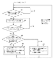
図4はプローブアクティビティ及びノードアイドルネス予測に基づいてキャッシュフラッシュするための実施形態の例示的なフロー図を示している。ステップ401において処理ノードがアイドル状態にある場合には、処理ノードはステップ402においてプローブアクティビティを追跡し、そしてステップ403において、プローブスレッショルドよりも大きいプローブアクティビティをノードがチェックする。次いでステップ405においては、処理ノードアイドルネスがアイドルスレッショルドよりも大きいと予測されるかどうかをフローがチェックする。予測される場合には、ステップ407において処理ノードは、そのキャッシュをフラッシュし、そのキャッシュシステムを無効化し、保持電圧又は他の適切な電力節約電圧を印加し、そしてシステムはノードをプローブすることを停止する。一方、ノードアイドルネスの予測された期間がスレッショルドを下回る場合、キャッシュフラッシュすることは、電力を節約せず又は十分な電力を節約しないのでそれほど魅力的ではなく、P状態制御アルゴリズム(上述した)がステップ409で適用されてよく、そしてノードはプローブアクティビティの追跡を継続し、必要であればプローブアクティビティのレベルに従ってP状態を調節する。
FIG. 4 shows an exemplary flow diagram of an embodiment for cache flushing based on probe activity and node idleness prediction. If the processing node is idle in
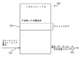
プローブアクティビティを追跡するための1つの実施形態は、ここではインフライトキュー(IFQ)と称される図5に示されるキュー構造を利用する。IFQ構造500は、プローブアクティビティのレベルを論理的に反映する多重エントリアレイである。任意のトランザクション(コヒーレント又は非コヒーレント)501は、IFQの利用可能なエントリ内へと置かれ、そして退去時点(eviction point)までそこにある。トランザクションは、応答ノードによる応答の後に、503で示されるようにIFQから割り当てを解除される(de-allocated)(退去させられる)。応答は、データ移動を含むトランザクションのためのデータフェーズ(即ち処理ノードから共有メモリへの又は共有メモリから処理ノードへのデータ移動)、又はデータ移動を伴わないトランザクションのための応答後フェーズ(即ちローカルキャッシュ内又は処理ノードのメモリ内のキャッシュを失効化するための要求)のいずれかであってよい。IFQ構造は、複数の処理ノード間で共有されてよく、又は処理ノード毎に例示化されて(instantiated)いてよい。プローブアクティビティのレベルは、アクティブなIFQエントリ(完了保留中の未決のコヒーレント要求が入っているエントリ)の数によって表される。
One embodiment for tracking probe activity utilizes the queue structure shown in FIG. 5, referred to herein as the in-flight queue (IFQ). The
1つの実施形態においては、ノード(又は制御機能があるどこでも)は、アクティブなIFQエントリの数を単一のスレッショルド502と比較する。尚、制御機能はノードの内部又は外部にあってよい。ノードの外部である場合には、上述したようなダイのアンコア部分内の同じダイ上にあってよい。エントリの数がスレッショルドを超える場合には、より高いP状態(最低P状態限界)への移行が生じる。ヒステリシスを差し引かれたスレッショルドよりも低いレベルにアクティブIFQエントリの数が落ちた後に、最低P状態限界性能フロアはキャンセルされ、そして処理ノードは、より低い電力で動作しながらより小さいプローブ帯域幅が対処され得る当座のP状態へと戻される。
In one embodiment, the node (or wherever there is a control function) compares the number of active IFQ entries with a
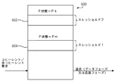
他の実施形態は図6に示される多重レベルIFQベースの手法を利用してよく、ここでは、各レベルは、異なるプローブ帯域幅に付随する関連する最低性能レベル(P状態スレッショルド)を有する。例えば16エントリIFQ構造600は、プローブ帯域幅における増大したニーズを表すP状態Pm及びPkにそれぞれ対応する2つのスレッショルド602及び604を有していてよい。状態間移行は、図3A及び3Bに示されるように達成されてよい。
Other embodiments may utilize the multi-level IFQ-based approach shown in FIG. 6, where each level has an associated minimum performance level (P-state threshold) associated with a different probe bandwidth. For example, the 16-
他の実施形態においては、プローブアクティビティを追跡するのに異なる手法が用いられてよい。例えば、プローブ要求に対して隠された、利用可能でない、又は追跡困難な完了フェーズを有するシステムにおいては、追跡手法は、異なるインクリメント速度及びデクリメント速度を伴うプローブカウントメカニズムに基づいていてよい。例えば図7を参照すると、新たなプローブ要求703が処理ノードに送られるたびに(CNT=CNT+w_inc)でインクリメントされるカウンタ701が示されている。カウント値は、処理ノードの特定のP状態に関連するプローブ速度(帯域幅)に合致する設定可能な時間インターバル(許容可能なインターバル(IntervalTolerated))毎に(CNT=CNT−w_dec)でデクリメントされる。ある実施形態においては、設定可能な時間インターバルは、特定のP状態に関連する最大プローブ帯域幅に合致する。このように、実際の応答(データ移動、データ移動を伴わないトランザクションのための応答フェーズ)が追跡されない場合であっても、プローブ要求が特定の速度でサービスされているものと仮定される。
In other embodiments, different approaches may be used to track probe activity. For example, in a system that has a completion phase that is hidden, unavailable, or difficult to track for probe requests, the tracking approach may be based on a probe count mechanism with different increment and decrement rates. For example, referring to FIG. 7, a
任意の新たなプローブ要求はカウンタを(CNT=CNT+w_inc)でインクリメントし、ここでw_incはカウンタの現在値に加えられる設定可能な重みである。幾つかの実施形態においては、インクリメント/デクリメント値は設定可能であってよく、またそれらの設定は、顧客、又はより高いレベルのソフトウエアの選択(性能バイアスされた、バランスされた、又は電力バイアスされた)に依存していてよい。性能バイアスされた設定に対しては、w_inc(インクリメント重み)はより大きな値に設定され、またw_dec(デクリメント重み)はより小さい値に設定される。電力節約バイアスされた設定に対しては、これらのパラメータは逆のやり方で設定されてよい。また、許容可能なインターバル(IntervalTolerated)値は、顧客又は高レベルソフトウエアの性能/電力の選択に依存して設定されてよい。カウンタ値は、プローブアクティビティのレベルを表し、そしてプローブアクティビティスレッショルドと比較されて最適P状態を導き出す。より大きなカウンタ値は、当座のP状態が満たすことのできない増大されたプローブ帯域幅に合致するために、より高い動作P状態を必要とする。 Any new probe request increments the counter by (CNT = CNT + w_inc), where w_inc is a configurable weight that is added to the current value of the counter. In some embodiments, the increment / decrement values may be configurable, and those settings may be selected by the customer, or higher level software (performance biased, balanced, or power bias). May be) dependent on. For performance biased settings, w_inc (increment weight) is set to a larger value and w_dec (decrement weight) is set to a smaller value. For power saving biased settings, these parameters may be set in the opposite manner. Also, an acceptable IntervalTolerated value may be set depending on the customer / high-level software performance / power selection. The counter value represents the level of probe activity and is compared to the probe activity threshold to derive the optimal P state. A larger counter value requires a higher operating P-state to match the increased probe bandwidth that the current P-state cannot meet.
ワークロード均一性を適切には表さず且つカウンタの過インクリメント及び性能/ワットの観点からは準最適であろう性能状態(P状態)の選択をもたらすプローブアクティビティのバーストを除去する(filter out)ために、ローパスフィルタ(LPF)705が用いられてよい。特定の実施形態によると、設定可能な数(1〜N)のプローブ要求が、設定可能なインターバルTの間に追跡される。プローブ要求の過カウンティングを、それらの出現が時間インターバルの間の何らかの設定可能な限界を超える場合に回避するために、ローパスフィルタは種々の方法で設定されてよい。例えばローパスフィルタは、インターバルTの間のn(1≦n≦N)個以下のプローブイベントを追跡するように実装されてよい。従って、プローブイベントの数がnより大きい場合には、カウンタはnだけをカウントする。ローパスフィルタは、フィルタリングされたプローブ要求をカウンタに供給する。 Filter out bursts of probe activity that do not adequately represent workload uniformity and result in selection of performance states (P states) that would be sub-optimal in terms of counter over-increment and performance / watts Therefore, a low-pass filter (LPF) 705 may be used. According to a particular embodiment, a configurable number (1-N) of probe requests are tracked during a configurable interval T. In order to avoid over-counting of probe requests if their occurrence exceeds some configurable limit during the time interval, the low pass filter may be set in various ways. For example, a low pass filter may be implemented to track n (1 ≦ n ≦ N) or less probe events during interval T. Thus, if the number of probe events is greater than n, the counter counts only n. The low pass filter supplies the filtered probe request to the counter.
代替的には、ローパスフィルタ705は、多重インターバルTにわたるプローブイベントの数を平均化するように実装されてよく、その結果、特定のインターバルTが高バーストのアクティビティを有してしまったとしても、その高バーストは、多重インターバルにわたる平均化によって制限される。平均化は例えば移動平均として実装されてよい。1つの実施形態においては、プローブ要求は、移動平均よりも高速度ではカウンタに供給されない。
Alternatively, the
言うまでもなく、ローパスフィルタの実装は、重みw_incがどのように決定されるかに影響するであろう。従って、例えば多数の時間インターバルにわたる平均化が用いられる場合には、重みは時間インターバルを反映するようにスケーリングされてよい。他の実施形態においては、フィルタリングせずにプローブ要求が直接カウンタに供給されてよい。 Needless to say, the implementation of the low-pass filter will affect how the weight w_inc is determined. Thus, for example, if averaging over multiple time intervals is used, the weights may be scaled to reflect the time interval. In other embodiments, probe requests may be provided directly to the counter without filtering.
ここでの実施形態の態様は、図1に示されるプロセッサに関連する揮発性又は不揮発性のメモリに記憶されるソフトウエアにおいて部分的に実装されてよい。ソフトウエアはコンピュータシステムの不揮発性部分に記憶されていてよく、揮発性メモリにロードされてよく、そして実行されてよい。このように、本発明の実施形態は、不揮発性メモリ等の機械可読媒体によって提供される機械実行可能命令内で具現化される特徴又は処理を含んでいてよい。そのような媒体は、マイクロプロセッサ又は更に一般的にはコンピュータシステム等の機械によってアクセス可能な形態にあるデータを記憶する任意のメカニズムを含んでいてよい。機械可読媒体は、リードオンリメモリ(ROM)、ランダムアクセスメモリ(RAM)、磁気ディスク記憶媒体、光学的記憶媒体、フラッシュメモリデバイス、テープ、又は他の磁気的、光学的、若しくは電子的な記憶媒体、等の揮発性メモリ及び/又は不揮発性メモリを含んでいてよい。そのような記憶されている命令は、命令がプログラムされる汎用又は専用のプロセッサに本発明の処理を実行させるために用いられ得る。 Aspects of the embodiments herein may be partially implemented in software stored in volatile or non-volatile memory associated with the processor shown in FIG. The software may be stored in a non-volatile part of the computer system, loaded into volatile memory, and executed. Thus, embodiments of the invention may include features or processes embodied in machine-executable instructions provided by a machine-readable medium, such as non-volatile memory. Such a medium may include any mechanism for storing data in a form accessible by a machine such as a microprocessor or more generally a computer system. The machine readable medium is a read only memory (ROM), a random access memory (RAM), a magnetic disk storage medium, an optical storage medium, a flash memory device, a tape, or other magnetic, optical or electronic storage medium. , Etc., and / or non-volatile memory. Such stored instructions can be used to cause a general purpose or special purpose processor in which the instructions are programmed to perform the processing of the present invention.
尚、本発明の幾つかの処理は、プログラムされた命令に応答するハードウエア動作を含んでいてよい。代替的には、本発明の処理は、動作を行う状態マシン等のハードワイヤード論理を含む特定のハードウエアコンポーネントによって、又はプログラムされたデータ処理コンポーネント及びハードウエアコンポーネントの任意の組み合わせによって行われてよい。このように、本発明の実施形態は、ここに説明されるようなソフトウエア、データ処理ハードウエア、システム実装のデータ処理方法、及び種々の処理動作を含んでいてよい。 Note that some processes of the present invention may include hardware operations that respond to programmed instructions. Alternatively, the processing of the present invention may be performed by a specific hardware component that includes hardwired logic, such as a state machine that performs operations, or by any combination of programmed data processing and hardware components. . Thus, embodiments of the present invention may include software, data processing hardware, system-implemented data processing methods, and various processing operations as described herein.
以上のように、種々の実施形態が説明されてきた。尚、ここに記載される本発明の説明は例示的なものであり、以下の特許請求の範囲に記載される本発明の範囲を限定することが意図されるものではない。以下の特許請求の範囲に記載される本発明の範囲から逸脱することなしに、ここに記載される説明に基づいて、ここに説明される実施形態の変形及び修正がなされてよい。 As described above, various embodiments have been described. It should be noted that the description of the invention described herein is exemplary and is not intended to limit the scope of the invention described in the claims below. Variations and modifications of the embodiments described herein may be made based on the description provided herein without departing from the scope of the invention as set forth in the following claims.
Claims (14)
前記プローブアクティビティレベルを第1のスレッショルドプローブアクティビティレベルと比較することと、
前記プローブアクティビティレベルが前記第1のスレッショルドプローブアクティビティレベルを超えている場合に前記処理ノードの性能状態を当座の性能状態よりも高い第1の性能状態に上げることと、を備える方法。 Tracking probe activity levels at processing nodes;
Comparing the probe activity level to a first threshold probe activity level;
Raising the performance state of the processing node to a first performance state that is higher than the current performance state when the probe activity level exceeds the first threshold probe activity level.
前記プローブアクティビティレベルが前記第2のスレッショルドプローブアクティビティレベルを超えて増大することに応答して前記処理ノードの前記性能状態を前記第3の性能状態に上げた後に前記性能状態を下げることと、を更に備える請求項1〜4のいずれかに記載の方法。 In response to the probe activity level increasing beyond a second threshold probe activity level that is higher than the first threshold probe activity level, the performance state of the processing node is higher than the first performance state. To a third performance state,
Lowering the performance state after raising the performance state of the processing node to the third performance state in response to the probe activity level increasing beyond the second threshold probe activity level; The method according to claim 1, further comprising:
各プローブ要求をキュー内にエンターすること並びにデータ移動及び応答の少なくとも一方を伴うプローブ要求に前記処理ノードが応答した後に前記プローブ要求を前記キューからリタイヤさせることと、
前記キュー内のエントリの数を前記第1のスレッショルドプローブアクティビティレベルと比較して前記プローブアクティビティが前記第1のスレッショルドプローブアクティビティレベルを上回っているかどうかを決定することと、を更に備える請求項1〜4のいずれかに記載の方法。 Tracking the probe activity includes
Entering each probe request into a queue and causing the probe request to be retired from the queue after the processing node responds to a probe request with at least one of data movement and response;
Comparing the number of entries in the queue with the first threshold probe activity level to determine whether the probe activity is above the first threshold probe activity level. 5. The method according to any one of 4.
前記装置は前記プローブアクティビティレベルが第1のスレッショルドプローブアクティビティレベルを超えて増大する場合に前記処理ノードの性能状態を当座の性能状態から第1の性能状態に上げるように動作し、
前記装置は前記第1のスレッショルドプローブアクティビティレベルより低い予め定められたレベルまで前記プローブアクティビティレベルが下がることに応答して前記第1の性能状態よりも低い第2の性能状態に前記処理ノードをエンターさせ、
前記第1及び第2の性能状態は電圧及び周波数の少なくとも一方によって定義される装置。 An apparatus comprising a probe tracker that tracks probe activity levels at a processing node,
The apparatus operates to raise the performance state of the processing node from an immediate performance state to a first performance state when the probe activity level increases above a first threshold probe activity level;
The apparatus enters the processing node into a second performance state that is lower than the first performance state in response to the probe activity level falling to a predetermined level that is lower than the first threshold probe activity level. Let
The apparatus wherein the first and second performance states are defined by at least one of voltage and frequency.
前記キュー内にプローブ要求がエンターされ、データ移動及び応答の少なくとも一方を伴うプローブ要求に前記処理ノードが応答した後に前記キュー内の前記プローブ要求は前記キューからリタイヤさせられ、
前記装置は前記キュー内のエントリの数を前記第1のスレッショルドプローブアクティビティレベルと比較して前記プローブアクティビティが第1のスレッショルドプローブアクティビティレベルを上回っているかどうかを決定するように動作可能である請求項10〜12のいずれかに記載の装置。 The probe tracker further comprises a cue;
A probe request is entered in the queue, and the probe request in the queue is retired from the queue after the processing node responds to a probe request with data movement and / or response.
The apparatus is operable to compare the number of entries in the queue with the first threshold probe activity level to determine whether the probe activity is above a first threshold probe activity level. The apparatus in any one of 10-12.
Applications Claiming Priority (5)
| Application Number | Priority Date | Filing Date | Title |
|---|---|---|---|
| US25879809P | 2009-11-06 | 2009-11-06 | |
| US61/258,798 | 2009-11-06 | ||
| US12/623,997 US20110112798A1 (en) | 2009-11-06 | 2009-11-23 | Controlling performance/power by frequency control of the responding node |
| US12/623,997 | 2009-11-23 | ||
| PCT/US2010/055598 WO2011057059A1 (en) | 2009-11-06 | 2010-11-05 | Controlling performance state by tracking probe activity level |
Publications (2)
| Publication Number | Publication Date |
|---|---|
| JP2013510376A true JP2013510376A (en) | 2013-03-21 |
| JP2013510376A5 JP2013510376A5 (en) | 2013-09-26 |
Family
ID=43536579
Family Applications (1)
| Application Number | Title | Priority Date | Filing Date |
|---|---|---|---|
| JP2012538025A Pending JP2013510376A (en) | 2009-11-06 | 2010-11-05 | Control performance state by tracking probe activity levels |
Country Status (6)
| Country | Link |
|---|---|
| US (2) | US20110112798A1 (en) |
| EP (1) | EP2497001A1 (en) |
| JP (1) | JP2013510376A (en) |
| KR (1) | KR20120102629A (en) |
| CN (1) | CN102667665A (en) |
| WO (1) | WO2011057059A1 (en) |
Families Citing this family (24)
| Publication number | Priority date | Publication date | Assignee | Title |
|---|---|---|---|---|
| US8566628B2 (en) * | 2009-05-06 | 2013-10-22 | Advanced Micro Devices, Inc. | North-bridge to south-bridge protocol for placing processor in low power state |
| US20110112798A1 (en) * | 2009-11-06 | 2011-05-12 | Alexander Branover | Controlling performance/power by frequency control of the responding node |
| US8635381B2 (en) * | 2010-08-26 | 2014-01-21 | International Business Machines Corporation | System, method and computer program product for monitoring memory access |
| US8930589B2 (en) * | 2010-08-26 | 2015-01-06 | International Business Machines Corporation | System, method and computer program product for monitoring memory access |
| US8438416B2 (en) * | 2010-10-21 | 2013-05-07 | Advanced Micro Devices, Inc. | Function based dynamic power control |
| US20120166731A1 (en) * | 2010-12-22 | 2012-06-28 | Christian Maciocco | Computing platform power management with adaptive cache flush |
| JP5674613B2 (en) * | 2011-09-22 | 2015-02-25 | 株式会社東芝 | Control system, control method and program |
| US9110671B2 (en) * | 2012-12-21 | 2015-08-18 | Advanced Micro Devices, Inc. | Idle phase exit prediction |
| US9600058B2 (en) * | 2014-06-24 | 2017-03-21 | Intel Corporation | Enhancing power-performance efficiency in a computer system when bursts of activity occurs when operating in low power |
| US20160116954A1 (en) * | 2014-10-28 | 2016-04-28 | Linkedln Corporation | Dynamic adjustment of cpu operating frequency |
| WO2016099567A1 (en) * | 2014-12-19 | 2016-06-23 | Hewlett Packard Enterprise Development Lp | Flushing data content in response to a power loss event to a processor |
| US9785223B2 (en) * | 2014-12-25 | 2017-10-10 | Intel Corporation | Power management in an uncore fabric |
| US9690708B2 (en) | 2015-05-19 | 2017-06-27 | Qualcomm Incorporated | Real-time cache behavior forecast using hypothetical cache |
| CN105068639B (en) * | 2015-07-29 | 2018-06-19 | Tcl移动通信科技(宁波)有限公司 | A kind of method and system of dynamic control processor frequencies |
| US11289133B2 (en) * | 2015-09-16 | 2022-03-29 | Arm Limited | Power state based data retention |
| US10324519B2 (en) * | 2016-06-23 | 2019-06-18 | Intel Corporation | Controlling forced idle state operation in a processor |
| US10120806B2 (en) | 2016-06-27 | 2018-11-06 | Intel Corporation | Multi-level system memory with near memory scrubbing based on predicted far memory idle time |
| US10216256B2 (en) | 2016-10-03 | 2019-02-26 | Microsoft Technology Licensing, Llc | Power conservation of computing components using forced idle state |
| US10180793B2 (en) * | 2017-01-31 | 2019-01-15 | Hewlett Packard Enterprise Development Lp | Performance attributes for memory |
| WO2019004880A1 (en) * | 2017-06-27 | 2019-01-03 | Telefonaktiebolaget Lm Ericsson (Publ) | Power management of an event-based processing system |
| US10725848B2 (en) * | 2018-02-07 | 2020-07-28 | Intel Corporation | Supporting hang detection and data recovery in microprocessor systems |
| US10628321B2 (en) * | 2018-02-28 | 2020-04-21 | Qualcomm Incorporated | Progressive flush of cache memory |
| US10958555B2 (en) | 2019-03-15 | 2021-03-23 | Juniper Networks, Inc. | Real-time application-driven synthetic probing |
| US11960773B2 (en) * | 2020-07-31 | 2024-04-16 | Hewlett Packard Enterprise Development Lp | Modifying virtual persistent volumes based on analysis of performance metrics |
Citations (4)
| Publication number | Priority date | Publication date | Assignee | Title |
|---|---|---|---|---|
| JPH10268963A (en) * | 1997-03-28 | 1998-10-09 | Mitsubishi Electric Corp | Information processor |
| JP2002221958A (en) * | 2001-01-26 | 2002-08-09 | Nec Corp | Power-saving graphics controlling circuit |
| US20080276236A1 (en) * | 2007-05-02 | 2008-11-06 | Advanced Micro Devices, Inc. | Data processing device with low-power cache access mode |
| WO2008152790A1 (en) * | 2007-06-12 | 2008-12-18 | Panasonic Corporation | Multiprocessor control device, multiprocessor control method, and multiprocessor control circuit |
Family Cites Families (83)
| Publication number | Priority date | Publication date | Assignee | Title |
|---|---|---|---|---|
| EP0656579B1 (en) * | 1993-12-01 | 2003-05-21 | Advanced Micro Devices, Inc. | Power management for computer system and method therefor |
| US5541850A (en) * | 1994-05-17 | 1996-07-30 | Vlsi Technology, Inc. | Method and apparatus for forming an integrated circuit including a memory structure |
| AU3313795A (en) * | 1994-10-14 | 1996-04-26 | Compaq Computer Corporation | Circuit for placing a cache memory into low power mode in response to special bus cycles |
| US5530932A (en) * | 1994-12-23 | 1996-06-25 | Intel Corporation | Cache coherent multiprocessing computer system with reduced power operating features |
| US5737615A (en) * | 1995-04-12 | 1998-04-07 | Intel Corporation | Microprocessor power control in a multiprocessor computer system |
| US6282662B1 (en) * | 1995-08-04 | 2001-08-28 | Dell Usa, L.P. | Power management override for portable computers |
| US5740417A (en) * | 1995-12-05 | 1998-04-14 | Motorola, Inc. | Pipelined processor operating in different power mode based on branch prediction state of branch history bit encoded as taken weakly not taken and strongly not taken states |
| US5692202A (en) * | 1995-12-29 | 1997-11-25 | Intel Corporation | System, apparatus, and method for managing power in a computer system |
| US6125450A (en) * | 1996-12-19 | 2000-09-26 | Intel Corporation | Stop clock throttling in a computer processor through disabling bus masters |
| JP3819166B2 (en) * | 1998-11-27 | 2006-09-06 | ヒタチグローバルストレージテクノロジーズネザーランドビーブイ | Energy consumption reduction method |
| US6360337B1 (en) | 1999-01-27 | 2002-03-19 | Sun Microsystems, Inc. | System and method to perform histogrammic counting for performance evaluation |
| US6141283A (en) * | 1999-04-01 | 2000-10-31 | Intel Corporation | Method and apparatus for dynamically placing portions of a memory in a reduced power consumption state |
| US6510525B1 (en) * | 1999-04-26 | 2003-01-21 | Mediaq, Inc. | Method and apparatus to power up an integrated device from a low power state |
| US6711691B1 (en) * | 1999-05-13 | 2004-03-23 | Apple Computer, Inc. | Power management for computer systems |
| US6480965B1 (en) * | 1999-10-07 | 2002-11-12 | Intel Corporation | Power management method for a computer system having a hub interface architecture |
| US6496895B1 (en) * | 1999-11-01 | 2002-12-17 | Intel Corporation | Method and apparatus for intializing a hub interface |
| US6760852B1 (en) * | 2000-08-31 | 2004-07-06 | Advanced Micro Devices, Inc. | System and method for monitoring and controlling a power-manageable resource based upon activities of a plurality of devices |
| US6988214B1 (en) * | 2000-11-06 | 2006-01-17 | Dell Products L.P. | Processor power state transistions using separate logic control |
| US6493801B2 (en) * | 2001-01-26 | 2002-12-10 | Compaq Computer Corporation | Adaptive dirty-block purging |
| US7051218B1 (en) * | 2001-07-18 | 2006-05-23 | Advanced Micro Devices, Inc. | Message based power management |
| US7174467B1 (en) * | 2001-07-18 | 2007-02-06 | Advanced Micro Devices, Inc. | Message based power management in a multi-processor system |
| US7200544B1 (en) * | 2001-10-26 | 2007-04-03 | National Semiconductor Corporation | Systems for selectively disabling timing violations in hardware description language models of integrated circuits and methods of operating the same |
| US6976181B2 (en) * | 2001-12-20 | 2005-12-13 | Intel Corporation | Method and apparatus for enabling a low power mode for a processor |
| US6954864B2 (en) * | 2002-03-29 | 2005-10-11 | Intel Corporation | Method and apparatus for remotely placing a computing device into a low power state |
| US6920574B2 (en) * | 2002-04-29 | 2005-07-19 | Apple Computer, Inc. | Conserving power by reducing voltage supplied to an instruction-processing portion of a processor |
| US7028200B2 (en) * | 2002-05-15 | 2006-04-11 | Broadcom Corporation | Method and apparatus for adaptive power management of memory subsystem |
| US7152169B2 (en) * | 2002-11-29 | 2006-12-19 | Intel Corporation | Method for providing power management on multi-threaded processor by using SMM mode to place a physical processor into lower power state |
| US6971033B2 (en) * | 2003-01-10 | 2005-11-29 | Broadcom Corporation | Method and apparatus for improving bus master performance |
| US7162404B2 (en) * | 2003-04-28 | 2007-01-09 | International Business Machines Corporation | Method, system and program product for configuring a simulation model of a digital design |
| US7299370B2 (en) * | 2003-06-10 | 2007-11-20 | Intel Corporation | Method and apparatus for improved reliability and reduced power in a processor by automatic voltage control during processor idle states |
| US7356713B2 (en) * | 2003-07-31 | 2008-04-08 | International Business Machines Corporation | Method and apparatus for managing the power consumption of a data processing system |
| TWI307008B (en) * | 2003-08-14 | 2009-03-01 | Via Tech Inc | Computer system with power management and the method thereof |
| US7200762B2 (en) * | 2003-09-30 | 2007-04-03 | Intel Corporation | Providing a low-power state processor voltage in accordance with a detected processor type |
| US7178045B2 (en) * | 2003-12-30 | 2007-02-13 | Intel Corporation | Optimizing exit latency from an active power management state |
| US7159766B2 (en) * | 2004-01-20 | 2007-01-09 | Standard Microsystems Corporation | Peripheral device feature allowing processors to enter a low power state |
| TWI264634B (en) * | 2004-04-13 | 2006-10-21 | Acer Inc | Method for monitoring power state of computer system and apparatus therefor |
| US7315952B2 (en) * | 2004-06-02 | 2008-01-01 | Intel Corporation | Power state coordination between devices sharing power-managed resources |
| US7272741B2 (en) * | 2004-06-02 | 2007-09-18 | Intel Corporation | Hardware coordination of power management activities |
| KR20050120565A (en) | 2004-06-17 | 2005-12-22 | 인텔 코오퍼레이션 | Power state coordination between devices sharing power-managed resources |
| TWI259354B (en) * | 2004-06-25 | 2006-08-01 | Via Tech Inc | System and method of real-time power management |
| US7451333B2 (en) * | 2004-09-03 | 2008-11-11 | Intel Corporation | Coordinating idle state transitions in multi-core processors |
| US7360106B2 (en) * | 2004-08-05 | 2008-04-15 | Matsushita Electric Industrial Co., Ltd. | Power-saving processing unit, power-saving processing method and program record medium |
| US7711966B2 (en) * | 2004-08-31 | 2010-05-04 | Qualcomm Incorporated | Dynamic clock frequency adjustment based on processor load |
| US20080141265A1 (en) * | 2004-12-08 | 2008-06-12 | Electronics And Telecommunications Research Instit | Power Management Method for Platform and that Platform |
| US7694080B2 (en) * | 2004-12-29 | 2010-04-06 | Intel Corporation | Method and apparatus for providing a low power mode for a processor while maintaining snoop throughput |
| US7610497B2 (en) * | 2005-02-01 | 2009-10-27 | Via Technologies, Inc. | Power management system with a bridge logic having analyzers for monitoring data quantity to modify operating clock and voltage of the processor and main memory |
| TWI268424B (en) * | 2005-03-15 | 2006-12-11 | Uli Electronics Inc | Signal transmission method between computer system and peripherals adopting PCI express bus characterizing in saving power of transmitting signals |
| US7444526B2 (en) * | 2005-06-16 | 2008-10-28 | International Business Machines Corporation | Performance conserving method for reducing power consumption in a server system |
| US7454632B2 (en) * | 2005-06-16 | 2008-11-18 | Intel Corporation | Reducing computing system power through idle synchronization |
| US7373534B2 (en) * | 2005-06-23 | 2008-05-13 | Intel Corporation | Reducing storage data transfer interference with processor power management |
| US7475262B2 (en) * | 2005-06-29 | 2009-01-06 | Intel Corporation | Processor power management associated with workloads |
| US7562234B2 (en) * | 2005-08-25 | 2009-07-14 | Apple Inc. | Methods and apparatuses for dynamic power control |
| TWI286705B (en) * | 2005-09-06 | 2007-09-11 | Via Tech Inc | Power management method of central processing unit |
| US7472299B2 (en) * | 2005-09-30 | 2008-12-30 | Intel Corporation | Low power arbiters in interconnection routers |
| US7750912B2 (en) * | 2005-11-23 | 2010-07-06 | Advanced Micro Devices, Inc. | Integrating display controller into low power processor |
| US7487371B2 (en) * | 2005-12-16 | 2009-02-03 | Nvidia Corporation | Data path controller with integrated power management to manage power consumption of a computing device and its components |
| US7516342B2 (en) * | 2005-12-30 | 2009-04-07 | Intel Corporation | Method, apparatus and system to dynamically choose an optimum power state |
| US7861068B2 (en) * | 2006-03-07 | 2010-12-28 | Intel Corporation | Method and apparatus for using dynamic workload characteristics to control CPU frequency and voltage scaling |
| JP2009543172A (en) | 2006-06-27 | 2009-12-03 | コーニンクレッカ フィリップス エレクトロニクス エヌ ヴィ | Apparatus and method for managing power consumption of multiple data processing units |
| US7644293B2 (en) * | 2006-06-29 | 2010-01-05 | Intel Corporation | Method and apparatus for dynamically controlling power management in a distributed system |
| US7930564B2 (en) * | 2006-07-31 | 2011-04-19 | Intel Corporation | System and method for controlling processor low power states |
| US7752474B2 (en) * | 2006-09-22 | 2010-07-06 | Apple Inc. | L1 cache flush when processor is entering low power mode |
| FR2906624A1 (en) * | 2006-10-03 | 2008-04-04 | Bull S A S Soc Par Actions Sim | Generated data storing system, has management module utilizing calculation result for managing priorities in accessing time by system for copying data of new volumes of virtual bookshop to virtual volumes of physical bookshop |
| US7949887B2 (en) * | 2006-11-01 | 2011-05-24 | Intel Corporation | Independent power control of processing cores |
| US20090150696A1 (en) * | 2007-12-10 | 2009-06-11 | Justin Song | Transitioning a processor package to a low power state |
| US7966506B2 (en) * | 2007-12-12 | 2011-06-21 | Intel Corporation | Saving power in a computer system |
| GB2455744B (en) * | 2007-12-19 | 2012-03-14 | Advanced Risc Mach Ltd | Hardware driven processor state storage prior to entering a low power mode |
| US8156362B2 (en) * | 2008-03-11 | 2012-04-10 | Globalfoundries Inc. | Hardware monitoring and decision making for transitioning in and out of low-power state |
| US8448002B2 (en) * | 2008-04-10 | 2013-05-21 | Nvidia Corporation | Clock-gated series-coupled data processing modules |
| US8131948B2 (en) * | 2008-08-29 | 2012-03-06 | Freescale Semiconductor, Inc. | Snoop request arbitration in a data processing system |
| US8112651B2 (en) * | 2008-09-25 | 2012-02-07 | Intel Corporation | Conserving power in a computer system |
| US8209559B2 (en) * | 2008-12-24 | 2012-06-26 | Intel Corporation | Low power polling techniques |
| US8195887B2 (en) * | 2009-01-21 | 2012-06-05 | Globalfoundries Inc. | Processor power management and method |
| US8725953B2 (en) * | 2009-01-21 | 2014-05-13 | Arm Limited | Local cache power control within a multiprocessor system |
| US8566628B2 (en) * | 2009-05-06 | 2013-10-22 | Advanced Micro Devices, Inc. | North-bridge to south-bridge protocol for placing processor in low power state |
| US8190939B2 (en) * | 2009-06-26 | 2012-05-29 | Microsoft Corporation | Reducing power consumption of computing devices by forecasting computing performance needs |
| US8443209B2 (en) * | 2009-07-24 | 2013-05-14 | Advanced Micro Devices, Inc. | Throttling computational units according to performance sensitivity |
| US8291249B2 (en) * | 2009-09-25 | 2012-10-16 | Advanced Micro Devices, Inc. | Method and apparatus for transitioning devices between power states based on activity request frequency |
| US20110112798A1 (en) * | 2009-11-06 | 2011-05-12 | Alexander Branover | Controlling performance/power by frequency control of the responding node |
| US8780121B2 (en) * | 2009-12-22 | 2014-07-15 | Intel Corporation | Graphics render clock throttling and gating mechanism for power saving |
| US8656198B2 (en) * | 2010-04-26 | 2014-02-18 | Advanced Micro Devices | Method and apparatus for memory power management |
| US8782456B2 (en) * | 2010-06-01 | 2014-07-15 | Intel Corporation | Dynamic and idle power reduction sequence using recombinant clock and power gating |
| US8352685B2 (en) * | 2010-08-20 | 2013-01-08 | Apple Inc. | Combining write buffer with dynamically adjustable flush metrics |
-
2009
- 2009-11-23 US US12/623,997 patent/US20110112798A1/en not_active Abandoned
-
2010
- 2010-02-08 US US12/702,085 patent/US9021209B2/en active Active
- 2010-11-05 KR KR1020127011940A patent/KR20120102629A/en not_active Application Discontinuation
- 2010-11-05 CN CN201080048873XA patent/CN102667665A/en active Pending
- 2010-11-05 EP EP10784608A patent/EP2497001A1/en not_active Withdrawn
- 2010-11-05 WO PCT/US2010/055598 patent/WO2011057059A1/en active Application Filing
- 2010-11-05 JP JP2012538025A patent/JP2013510376A/en active Pending
Patent Citations (5)
| Publication number | Priority date | Publication date | Assignee | Title |
|---|---|---|---|---|
| JPH10268963A (en) * | 1997-03-28 | 1998-10-09 | Mitsubishi Electric Corp | Information processor |
| JP2002221958A (en) * | 2001-01-26 | 2002-08-09 | Nec Corp | Power-saving graphics controlling circuit |
| US20080276236A1 (en) * | 2007-05-02 | 2008-11-06 | Advanced Micro Devices, Inc. | Data processing device with low-power cache access mode |
| JP2010526374A (en) * | 2007-05-02 | 2010-07-29 | アドバンスト・マイクロ・ディバイシズ・インコーポレイテッド | Data processing device with low power cache access mode |
| WO2008152790A1 (en) * | 2007-06-12 | 2008-12-18 | Panasonic Corporation | Multiprocessor control device, multiprocessor control method, and multiprocessor control circuit |
Also Published As
| Publication number | Publication date |
|---|---|
| WO2011057059A1 (en) | 2011-05-12 |
| US20110113202A1 (en) | 2011-05-12 |
| US9021209B2 (en) | 2015-04-28 |
| CN102667665A (en) | 2012-09-12 |
| EP2497001A1 (en) | 2012-09-12 |
| US20110112798A1 (en) | 2011-05-12 |
| KR20120102629A (en) | 2012-09-18 |
Similar Documents
| Publication | Publication Date | Title |
|---|---|---|
| JP2013510376A (en) | Control performance state by tracking probe activity levels | |
| US10564699B2 (en) | Dynamically controlling cache size to maximize energy efficiency | |
| US9618997B2 (en) | Controlling a turbo mode frequency of a processor | |
| US9372524B2 (en) | Dynamically modifying a power/performance tradeoff based on processor utilization | |
| US9074947B2 (en) | Estimating temperature of a processor core in a low power state without thermal sensor information | |
| US20050125702A1 (en) | Method and system for power management including device controller-based device use evaluation and power-state control | |
| US10204056B2 (en) | Dynamic cache enlarging by counting evictions | |
| CN107153455B (en) | Cache power management | |
| US9075609B2 (en) | Power controller, processor and method of power management | |
| US9965023B2 (en) | Apparatus and method for flushing dirty cache lines based on cache activity levels | |
| TW202414188A (en) | Computing system and method of a computing system for performing partial cache deactivation | |
| EP4339789A1 (en) | Dynamic cache resource allocation for quality of service and system power reduction | |
| CN117707997A (en) | Computing system and method for partial cache deactivation of computing system | |
| CN117707996A (en) | Computing system and method for sharing cache allocation by same | |
| EP4314988A1 (en) | Systems and methods for processing asynchronous reset events while maintaining persistent memory state | |
| KR101024073B1 (en) | An Shared L2 Leakage Energy Management Method and Apparatus | |
| CN111177023A (en) | Method and device for distributing storage intervals in embedded equipment |
Legal Events
| Date | Code | Title | Description |
|---|---|---|---|
| A521 | Written amendment |
Free format text: JAPANESE INTERMEDIATE CODE: A523 Effective date: 20130808 |
|
| A621 | Written request for application examination |
Free format text: JAPANESE INTERMEDIATE CODE: A621 Effective date: 20130808 |
|
| A977 | Report on retrieval |
Free format text: JAPANESE INTERMEDIATE CODE: A971007 Effective date: 20140528 |
|
| A131 | Notification of reasons for refusal |
Free format text: JAPANESE INTERMEDIATE CODE: A131 Effective date: 20140625 |
|
| A02 | Decision of refusal |
Free format text: JAPANESE INTERMEDIATE CODE: A02 Effective date: 20150106 |