JP2013504188A - Conversion means body, optoelectronic semiconductor chip, and method of manufacturing optoelectronic semiconductor chip - Google Patents
Conversion means body, optoelectronic semiconductor chip, and method of manufacturing optoelectronic semiconductor chip Download PDFInfo
- Publication number
- JP2013504188A JP2013504188A JP2012527269A JP2012527269A JP2013504188A JP 2013504188 A JP2013504188 A JP 2013504188A JP 2012527269 A JP2012527269 A JP 2012527269A JP 2012527269 A JP2012527269 A JP 2012527269A JP 2013504188 A JP2013504188 A JP 2013504188A
- Authority
- JP
- Japan
- Prior art keywords
- conversion means
- means body
- semiconductor chip
- shore
- matrix material
- Prior art date
- Legal status (The legal status is an assumption and is not a legal conclusion. Google has not performed a legal analysis and makes no representation as to the accuracy of the status listed.)
- Pending
Links
Images


Classifications
-
- H—ELECTRICITY
- H01—ELECTRIC ELEMENTS
- H01L—SEMICONDUCTOR DEVICES NOT COVERED BY CLASS H10
- H01L33/00—Semiconductor devices with at least one potential-jump barrier or surface barrier specially adapted for light emission; Processes or apparatus specially adapted for the manufacture or treatment thereof or of parts thereof; Details thereof
- H01L33/48—Semiconductor devices with at least one potential-jump barrier or surface barrier specially adapted for light emission; Processes or apparatus specially adapted for the manufacture or treatment thereof or of parts thereof; Details thereof characterised by the semiconductor body packages
- H01L33/50—Wavelength conversion elements
- H01L33/501—Wavelength conversion elements characterised by the materials, e.g. binder
-
- C—CHEMISTRY; METALLURGY
- C09—DYES; PAINTS; POLISHES; NATURAL RESINS; ADHESIVES; COMPOSITIONS NOT OTHERWISE PROVIDED FOR; APPLICATIONS OF MATERIALS NOT OTHERWISE PROVIDED FOR
- C09K—MATERIALS FOR MISCELLANEOUS APPLICATIONS, NOT PROVIDED FOR ELSEWHERE
- C09K11/00—Luminescent, e.g. electroluminescent, chemiluminescent materials
- C09K11/08—Luminescent, e.g. electroluminescent, chemiluminescent materials containing inorganic luminescent materials
-
- H—ELECTRICITY
- H01—ELECTRIC ELEMENTS
- H01L—SEMICONDUCTOR DEVICES NOT COVERED BY CLASS H10
- H01L24/00—Arrangements for connecting or disconnecting semiconductor or solid-state bodies; Methods or apparatus related thereto
- H01L24/01—Means for bonding being attached to, or being formed on, the surface to be connected, e.g. chip-to-package, die-attach, "first-level" interconnects; Manufacturing methods related thereto
- H01L24/18—High density interconnect [HDI] connectors; Manufacturing methods related thereto
- H01L24/23—Structure, shape, material or disposition of the high density interconnect connectors after the connecting process
- H01L24/24—Structure, shape, material or disposition of the high density interconnect connectors after the connecting process of an individual high density interconnect connector
-
- H—ELECTRICITY
- H01—ELECTRIC ELEMENTS
- H01L—SEMICONDUCTOR DEVICES NOT COVERED BY CLASS H10
- H01L33/00—Semiconductor devices with at least one potential-jump barrier or surface barrier specially adapted for light emission; Processes or apparatus specially adapted for the manufacture or treatment thereof or of parts thereof; Details thereof
- H01L33/48—Semiconductor devices with at least one potential-jump barrier or surface barrier specially adapted for light emission; Processes or apparatus specially adapted for the manufacture or treatment thereof or of parts thereof; Details thereof characterised by the semiconductor body packages
- H01L33/50—Wavelength conversion elements
- H01L33/508—Wavelength conversion elements having a non-uniform spatial arrangement or non-uniform concentration, e.g. patterned wavelength conversion layer, wavelength conversion layer with a concentration gradient of the wavelength conversion material
-
- H—ELECTRICITY
- H05—ELECTRIC TECHNIQUES NOT OTHERWISE PROVIDED FOR
- H05B—ELECTRIC HEATING; ELECTRIC LIGHT SOURCES NOT OTHERWISE PROVIDED FOR; CIRCUIT ARRANGEMENTS FOR ELECTRIC LIGHT SOURCES, IN GENERAL
- H05B33/00—Electroluminescent light sources
- H05B33/10—Apparatus or processes specially adapted to the manufacture of electroluminescent light sources
-
- H—ELECTRICITY
- H05—ELECTRIC TECHNIQUES NOT OTHERWISE PROVIDED FOR
- H05B—ELECTRIC HEATING; ELECTRIC LIGHT SOURCES NOT OTHERWISE PROVIDED FOR; CIRCUIT ARRANGEMENTS FOR ELECTRIC LIGHT SOURCES, IN GENERAL
- H05B33/00—Electroluminescent light sources
- H05B33/12—Light sources with substantially two-dimensional radiating surfaces
- H05B33/14—Light sources with substantially two-dimensional radiating surfaces characterised by the chemical or physical composition or the arrangement of the electroluminescent material, or by the simultaneous addition of the electroluminescent material in or onto the light source
- H05B33/145—Arrangements of the electroluminescent material
-
- H—ELECTRICITY
- H01—ELECTRIC ELEMENTS
- H01L—SEMICONDUCTOR DEVICES NOT COVERED BY CLASS H10
- H01L2224/00—Indexing scheme for arrangements for connecting or disconnecting semiconductor or solid-state bodies and methods related thereto as covered by H01L24/00
- H01L2224/01—Means for bonding being attached to, or being formed on, the surface to be connected, e.g. chip-to-package, die-attach, "first-level" interconnects; Manufacturing methods related thereto
- H01L2224/42—Wire connectors; Manufacturing methods related thereto
- H01L2224/47—Structure, shape, material or disposition of the wire connectors after the connecting process
- H01L2224/48—Structure, shape, material or disposition of the wire connectors after the connecting process of an individual wire connector
- H01L2224/4805—Shape
- H01L2224/4809—Loop shape
- H01L2224/48091—Arched
-
- H—ELECTRICITY
- H01—ELECTRIC ELEMENTS
- H01L—SEMICONDUCTOR DEVICES NOT COVERED BY CLASS H10
- H01L2224/00—Indexing scheme for arrangements for connecting or disconnecting semiconductor or solid-state bodies and methods related thereto as covered by H01L24/00
- H01L2224/01—Means for bonding being attached to, or being formed on, the surface to be connected, e.g. chip-to-package, die-attach, "first-level" interconnects; Manufacturing methods related thereto
- H01L2224/42—Wire connectors; Manufacturing methods related thereto
- H01L2224/47—Structure, shape, material or disposition of the wire connectors after the connecting process
- H01L2224/48—Structure, shape, material or disposition of the wire connectors after the connecting process of an individual wire connector
- H01L2224/481—Disposition
- H01L2224/48151—Connecting between a semiconductor or solid-state body and an item not being a semiconductor or solid-state body, e.g. chip-to-substrate, chip-to-passive
- H01L2224/48221—Connecting between a semiconductor or solid-state body and an item not being a semiconductor or solid-state body, e.g. chip-to-substrate, chip-to-passive the body and the item being stacked
- H01L2224/48225—Connecting between a semiconductor or solid-state body and an item not being a semiconductor or solid-state body, e.g. chip-to-substrate, chip-to-passive the body and the item being stacked the item being non-metallic, e.g. insulating substrate with or without metallisation
- H01L2224/48227—Connecting between a semiconductor or solid-state body and an item not being a semiconductor or solid-state body, e.g. chip-to-substrate, chip-to-passive the body and the item being stacked the item being non-metallic, e.g. insulating substrate with or without metallisation connecting the wire to a bond pad of the item
-
- H—ELECTRICITY
- H01—ELECTRIC ELEMENTS
- H01L—SEMICONDUCTOR DEVICES NOT COVERED BY CLASS H10
- H01L2924/00—Indexing scheme for arrangements or methods for connecting or disconnecting semiconductor or solid-state bodies as covered by H01L24/00
- H01L2924/10—Details of semiconductor or other solid state devices to be connected
- H01L2924/11—Device type
- H01L2924/12—Passive devices, e.g. 2 terminal devices
- H01L2924/1204—Optical Diode
- H01L2924/12041—LED
-
- H—ELECTRICITY
- H01—ELECTRIC ELEMENTS
- H01L—SEMICONDUCTOR DEVICES NOT COVERED BY CLASS H10
- H01L2924/00—Indexing scheme for arrangements or methods for connecting or disconnecting semiconductor or solid-state bodies as covered by H01L24/00
- H01L2924/10—Details of semiconductor or other solid state devices to be connected
- H01L2924/11—Device type
- H01L2924/12—Passive devices, e.g. 2 terminal devices
- H01L2924/1204—Optical Diode
- H01L2924/12043—Photo diode
-
- H—ELECTRICITY
- H01—ELECTRIC ELEMENTS
- H01L—SEMICONDUCTOR DEVICES NOT COVERED BY CLASS H10
- H01L2924/00—Indexing scheme for arrangements or methods for connecting or disconnecting semiconductor or solid-state bodies as covered by H01L24/00
- H01L2924/30—Technical effects
- H01L2924/35—Mechanical effects
- H01L2924/351—Thermal stress
-
- H—ELECTRICITY
- H01—ELECTRIC ELEMENTS
- H01L—SEMICONDUCTOR DEVICES NOT COVERED BY CLASS H10
- H01L2933/00—Details relating to devices covered by the group H01L33/00 but not provided for in its subgroups
- H01L2933/0008—Processes
- H01L2933/0033—Processes relating to semiconductor body packages
- H01L2933/0041—Processes relating to semiconductor body packages relating to wavelength conversion elements
-
- Y—GENERAL TAGGING OF NEW TECHNOLOGICAL DEVELOPMENTS; GENERAL TAGGING OF CROSS-SECTIONAL TECHNOLOGIES SPANNING OVER SEVERAL SECTIONS OF THE IPC; TECHNICAL SUBJECTS COVERED BY FORMER USPC CROSS-REFERENCE ART COLLECTIONS [XRACs] AND DIGESTS
- Y10—TECHNICAL SUBJECTS COVERED BY FORMER USPC
- Y10T—TECHNICAL SUBJECTS COVERED BY FORMER US CLASSIFICATION
- Y10T428/00—Stock material or miscellaneous articles
- Y10T428/31504—Composite [nonstructural laminate]
- Y10T428/31652—Of asbestos
- Y10T428/31663—As siloxane, silicone or silane
Landscapes
- Engineering & Computer Science (AREA)
- Microelectronics & Electronic Packaging (AREA)
- Computer Hardware Design (AREA)
- Power Engineering (AREA)
- Manufacturing & Machinery (AREA)
- Chemical & Material Sciences (AREA)
- Inorganic Chemistry (AREA)
- Materials Engineering (AREA)
- Organic Chemistry (AREA)
- Led Device Packages (AREA)
- Electroluminescent Light Sources (AREA)
Abstract
本発明は、オプトエレクトロニクス半導体チップの製造方法に関する。この製造方法の少なくとも一つの実施の形態においては、方法が、少なくとも一つの活性層を備えている半導体積層体(3)を準備するステップと、変換手段粒子(55)が埋め込まれているマトリクス材料(50)を有しているワンピースの変換手段体(5)を準備するステップであって、マトリクス材料は不完全に架橋されており、及び/又は、硬化されており、且つ、変換手段体は室温においてショアA0を上回り且つショアA35以下の硬度、及び/又は、10Pa・s以上150Pa・s以下の粘度を有するステップと、半導体積層体の上に変換手段体を取り付け、半導体積層体と変換手段体とを相互に直接的に接触させるステップと、変換手段体を硬化させるステップであって、硬化後に変換手段体の硬度は少なくともショアA30且つ最大でショアD80であるステップとを備えている。 The present invention relates to a method for manufacturing an optoelectronic semiconductor chip. In at least one embodiment of this manufacturing method, the method comprises the steps of providing a semiconductor stack (3) comprising at least one active layer, and a matrix material in which the conversion means particles (55) are embedded. Providing a one-piece conversion means body (5) having (50), wherein the matrix material is incompletely crosslinked and / or cured and the conversion means body is A step having a hardness exceeding Shore A0 at room temperature and having a hardness of Shore A35 or less and / or a viscosity of 10 Pa · s or more and 150 Pa · s or less; A step of bringing the body into direct contact with each other and a step of curing the conversion means body, the hardness of the conversion means body after curing being at least Shore A 0 and a maximum and a step is Shore D80.
Description
本発明は、変換手段体並びにその種の変換手段体を備えたオプトエレクトロニクス半導体チップに関する。更には、オプトエレクトロニクス半導体チップの製造方法が提供される。 The present invention relates to a conversion means body and an optoelectronic semiconductor chip provided with such a conversion means body. Furthermore, a method for manufacturing an optoelectronic semiconductor chip is provided.
本発明の解決すべき課題は、半導体積層体における高い固着性を有する変換手段体を提供することである。本発明の解決すべき別の課題は、その種の変換手段体を備えたオプトエレクトロニクス半導体チップを提供することである。本発明の解決すべき更に別の課題は、その種のオプトエレクトロニクス半導体チップの製造方法を提供することである。 The problem to be solved by the present invention is to provide a conversion means body having high adhesion in a semiconductor laminate. Another problem to be solved by the present invention is to provide an optoelectronic semiconductor chip comprising such a conversion means body. Yet another problem to be solved by the present invention is to provide a method of manufacturing such an optoelectronic semiconductor chip.
変換手段体の少なくとも一つの実施の形態によれば、この変換手段体は、オプトエレクトロニクス半導体チップに被着されるために設けられている。半導体チップとしてフォトダイオード、レーザダイオード、又は、有利には発光ダイオードが考えられる。特に、変換手段体は、半導体チップの寸法と同等の幾何学的な寸法を有している。例えば、半導体チップ及び/又は変換手段体の横方向の平均寸法は0.3mm以上10.0mm以下、特に0.5mm以上3.0mm以下である。 According to at least one embodiment of the conversion means body, this conversion means body is provided for attachment to an optoelectronic semiconductor chip. As a semiconductor chip, a photodiode, a laser diode, or preferably a light emitting diode can be considered. In particular, the conversion means body has a geometric dimension equivalent to that of the semiconductor chip. For example, the average lateral dimension of the semiconductor chip and / or the conversion means body is 0.3 mm or more and 10.0 mm or less, particularly 0.5 mm or more and 3.0 mm or less.
変換手段体の少なくとも一つの実施の形態によれば、この変換手段体はマトリクス材料と、このマトリクス材料内に埋め込まれている変換手段粒子とを有している。一種類の変換手段粒子又は複数の異なる種類の変換手段粒子を使用することができる。 According to at least one embodiment of the conversion means body, the conversion means body comprises a matrix material and conversion means particles embedded in the matrix material. One type of conversion means particles or a plurality of different types of conversion means particles can be used.
変換手段体の少なくとも一つの実施の形態によれば、マトリクス材料は不完全に硬化されている、及び/又は、不完全に架橋されている。換言すれば、マトリクス材料の硬度及び/又はヤング率を、別の硬化プロセス又は架橋プロセスによって高めることができる。 According to at least one embodiment of the conversion means body, the matrix material is incompletely cured and / or incompletely crosslinked. In other words, the hardness and / or Young's modulus of the matrix material can be increased by another curing or crosslinking process.
変換手段体の少なくとも一つの実施の形態によれば、この変換手段体は室温において、ショアA0を上回る硬度且つショアA35以下の硬度、又は、ショアA2以上ショアA15以下の硬度、及び/又は、10.0Pa・s以上150Pa・s以下の粘度、又は、15.0Pa・s以上70Pa・s以下の粘度を有している。室温とは特に約293Kの温度を意味している。即ち、不完全に硬化及び/又は架橋されたマトリクス材料を有している変換手段体は比較的柔らかい。 According to at least one embodiment of the conversion means body, this conversion means body has a hardness above Shore A0 and a hardness below Shore A35, or a hardness above Shore A2 and below Shore A15 and / or 10 at room temperature. It has a viscosity of 0.0 Pa · s to 150 Pa · s, or a viscosity of 15.0 Pa · s to 70 Pa · s. Room temperature means in particular a temperature of about 293K. That is, the conversion means having a matrix material that is incompletely cured and / or cross-linked is relatively soft.
オプトエレクトロニクス半導体チップのために設けられている変換手段体の少なくとも一つの実施の形態においては、この変換手段体はマトリクス材料と、このマトリクス材料内に埋め込まれている変換手段粒子とを有している。マトリクス材料は不完全に硬化されている、及び/又は、不完全に架橋されている。また、変換手段体は室温においてショアA10以上ショアA35以下の硬度、及び/又は、10Pa・s以上70Pa・s以下の粘度を示す。 In at least one embodiment of the conversion means provided for the optoelectronic semiconductor chip, the conversion means comprises a matrix material and conversion means particles embedded in the matrix material. Yes. The matrix material is incompletely cured and / or incompletely crosslinked. The conversion means body exhibits a hardness of Shore A10 to Shore A35 and / or a viscosity of 10 Pa · s to 70 Pa · s at room temperature.
変換手段体は不完全に硬化及び/又は架橋された状態で、形状結合(形状による束縛;formschluessig)により、半導体積層体に被着可能である。変換手段体の後続の硬化によって、変換手段体と半導体積層体との間の特に固い機械的な結合を達成することができる。これによって、半導体チップの寿命を延長することができる。 The conversion means body can be applied to the semiconductor stack by form bonding (formschluessig) in an incompletely cured and / or crosslinked state. By subsequent curing of the conversion means body, a particularly hard mechanical bond between the conversion means body and the semiconductor stack can be achieved. Thereby, the lifetime of the semiconductor chip can be extended.
変換手段体の少なくとも一つの実施の形態によれば、マトリクス材料はシリコーンを含有しているか、又は、その種の材料から構成されている。同様に、マトリクス材料はエポキシド又はシリコーン−エポキシドハイブリッド材料を含有することができるか、又は、その種の材料から構成されている。 According to at least one embodiment of the conversion means body, the matrix material contains silicone or is composed of such a material. Similarly, the matrix material can contain an epoxide or a silicone-epoxide hybrid material or is composed of such a material.
変換手段体の少なくとも一つの実施の形態によれば、この変換手段体はチキソトロピー剤を含有していない。特に、シリコーン用の長鎖基本材料の使用によって、及び/又は、マトリクス材料用の高粘度出発材料の使用によって、硬化していないマトリクス材料における変換手段粒子の分離及び/又は沈降を阻止できることが分かった。これによって、特に粒子として、とりわけナノ粒子として存在するチキソトロピー剤を省略することができる。 According to at least one embodiment of the conversion means body, the conversion means body does not contain a thixotropic agent. In particular, it has been found that the separation and / or settling of the conversion means particles in the uncured matrix material can be prevented by the use of a long chain base material for silicone and / or by the use of a high viscosity starting material for the matrix material. It was. This makes it possible to dispense with thixotropic agents which are present in particular as particles, in particular as nanoparticles.
変換手段体の少なくとも一つの実施の形態によれば、変換手段粒子の重量割合は20%以上75%以下、有利には55%以上70%以下である。換言すれば、変換手段体の重量割合の大部分は変換手段粒子によるものである。 According to at least one embodiment of the conversion means body, the weight proportion of the conversion means particles is not less than 20% and not more than 75%, preferably not less than 55% and not more than 70%. In other words, most of the weight ratio of the conversion means body is due to the conversion means particles.
変換手段体の少なくとも一つの実施の形態によれば、この変換手段体はワンピースで形成されている。即ち、変換手段体は一体的に形成されている。即ち、マトリクス材料は、変換手段粒子が埋め込まれている、繋がった中断の無い集合体を形成する。特に、この場合、変換手段体は複数の変換手段粒子を含有している部分領域を有していない。それらの変換粒子手段は、例えば、相境界によって相互に隔てられている、及び/又は、平均材料組成及び/又は物理的な特性が相互に異なっている。 According to at least one embodiment of the conversion means body, the conversion means body is formed in one piece. That is, the conversion means body is integrally formed. That is, the matrix material forms a connected uninterrupted assembly in which the conversion means particles are embedded. In particular, in this case, the conversion means body does not have a partial region containing a plurality of conversion means particles. These conversion particle means are separated from one another by, for example, phase boundaries and / or differ in average material composition and / or physical properties.
更には、例えば上述の実施形態の内の一つ又は複数の実施形態による変換手段体を有しているオプトエレクトロニクス半導体チップが提供される。従って、変換手段体の特徴は本発明によるオプトエレクトロニクス半導体チップに対しても開示されており、またその逆についても当てはまる。 Furthermore, for example, an optoelectronic semiconductor chip having a conversion means body according to one or more of the embodiments described above is provided. Therefore, the features of the conversion means are also disclosed for the optoelectronic semiconductor chip according to the invention and vice versa.
オプトエレクトロニクス半導体チップの少なくとも一つの実施の形態においては、このオプトエレクトロニクス半導体チップは、少なくとも一つの活性層を備えている半導体積層体を有している。更に半導体チップは、変換手段粒子が埋め込まれているマトリクス材料を有しているワンピースの変換手段体を含んでいる。変換手段体は、半導体積層体と直接的に接触しており、また更には、結合手段を介することなく半導体積層体上に取り付けられている。変換手段体の硬度は、少なくともショアA30且つ最大でショアD80、有利には少なくともショアA60且つ最大でショアD80、特に少なくともショアD30且つ最大でショアD75である。 In at least one embodiment of the optoelectronic semiconductor chip, the optoelectronic semiconductor chip comprises a semiconductor stack comprising at least one active layer. The semiconductor chip further includes a one-piece conversion means body having a matrix material in which the conversion means particles are embedded. The conversion means body is in direct contact with the semiconductor laminate, and is further mounted on the semiconductor laminate without any coupling means. The hardness of the conversion body is at least Shore A30 and at most Shore D80, preferably at least Shore A60 and at most Shore D80, in particular at least Shore D30 and at most Shore D75.
結合材料を介さないとは、半導体積層体と変換手段体との間に接着剤、接着フィルム又ははんだのような結合手段が存在しないことを意味している。半導体積層体及び変換手段体は少なくとも部分的に相互に直接的に接触しているということは、マトリクス材料が少なくとも部分的に半導体積層体の半導体材料と物理的に接触していることを意味している。 By not using a bonding material, it means that there is no bonding means such as an adhesive, an adhesive film or solder between the semiconductor laminate and the conversion means body. The fact that the semiconductor stack and the conversion means are at least partly in direct contact with each other means that the matrix material is at least partly in physical contact with the semiconductor material of the semiconductor stack. ing.
コンタクト構造が直接的に固定的で永続的に半導体材料と結合されている、及び/又は、半導体材料に一体的に結合されている場合、例えば半導体積層体の半導体材料上に直接的に取り付けられている電気的なコンタクト構造を半導体積層体に属するものと見なすことができる。即ち、半導体積層体と直接的に接触しているとは、変換手段体が、例えば金属又は透明導電性酸化物によって形成されている電気的なコンタクト構造上に直接的に取り付けられていることを意味している。 If the contact structure is directly fixed and permanently bonded to the semiconductor material and / or integrally bonded to the semiconductor material, it is mounted directly on the semiconductor material of the semiconductor stack, for example The electrical contact structure can be regarded as belonging to the semiconductor stack. That is, being in direct contact with the semiconductor stack means that the conversion means body is directly attached on an electrical contact structure formed of, for example, a metal or a transparent conductive oxide. I mean.
オプトエレクトロニクス半導体チップの少なくとも一つの実施の形態によれば、半導体積層体の放射通過面及び側面がそれぞれ少なくとも90%変換手段体によって覆われている。被覆度合いは特に、半導体積層体のそれぞれの側面に対して垂直な方向において決定することができる。 According to at least one embodiment of the optoelectronic semiconductor chip, the radiation passing surface and the side surface of the semiconductor stack are each covered by at least 90% conversion means. In particular, the degree of coverage can be determined in a direction perpendicular to the respective side surface of the semiconductor stack.
オプトエレクトロニクス半導体チップの少なくとも一つの実施の形態によれば、変換手段体が半導体積層体の少なくとも一つの境界面に形状結合により接触している。このことは、特に微視的なスケールにおいて、変換手段体及び境界面が相互に密着していることを意味している。特に、半導体積層体の粗面部を境界面における変換手段体によって模造することができる。これによって、特に微視的なスケールで、半導体積層体と変換手段体との間に噛合部を生じさせることができ、従って、変換手段体と半導体積層体との間の特に高い固着を達成することができる。同様に、半導体積層体と変換手段体との間のコンタクト面が拡大するので、付着力を介する固着性も増加する。変換手段体における半導体基体の境界面側とは反対側の面を平滑又は平坦に構成することができるので、例えばこの面においては粗面部は形成されていない。 According to at least one embodiment of the optoelectronic semiconductor chip, the conversion means body is in contact with at least one interface of the semiconductor stack by shape bonding. This means that the conversion means body and the boundary surface are in close contact with each other, particularly on a microscopic scale. In particular, the rough surface portion of the semiconductor laminate can be imitated by the conversion means body at the boundary surface. This makes it possible to produce a meshing part between the semiconductor stack and the conversion means body, in particular on a microscopic scale, and thus achieve a particularly high adhesion between the conversion means body and the semiconductor stack. be able to. Similarly, since the contact surface between the semiconductor stacked body and the conversion means body is enlarged, the fixing property via the adhesion force is also increased. Since the surface opposite to the boundary surface side of the semiconductor substrate in the conversion means body can be configured to be smooth or flat, for example, no rough surface portion is formed on this surface.
少なくとも一つの実施の形態によれば、半導体チップの側面、即ち、特に半導体チップの成長方向に並行な横方向の境界面は、最大で15%又は最大で5%まで変換手段体によって、側面に垂直な方向において覆われている。特に、側面は変換手段体によって覆われていない。 According to at least one embodiment, the side surface of the semiconductor chip, i.e. the lateral boundary, in particular parallel to the growth direction of the semiconductor chip, is applied to the side surface by the conversion means up to 15% or up to 5%. Covered in the vertical direction. In particular, the side surfaces are not covered by the conversion means body.
更には、オプトエレクトロニクス半導体チップの製造方法が提供される。半導体チップは、例えば、上述の実施形態の内の一つ又は複数に従い構成されている。従って、変換手段体並びにオプトエレクトロニクス半導体チップの特徴は本発明による方法に対しても開示されており、またその逆についても当てはまる。 Furthermore, a method for manufacturing an optoelectronic semiconductor chip is provided. The semiconductor chip is configured according to one or more of the above-described embodiments, for example. Thus, the features of the conversion means body as well as the optoelectronic semiconductor chip are disclosed for the method according to the invention and vice versa.
本方法の少なくとも一つの実施の形態においては、本方法が以下のステップを備えている:
−少なくとも一つの活性層を備えている半導体積層体を準備するステップ、
−変換手段粒子が埋め込まれているマトリクス材料を有しているワンピースの変換手段体を準備するステップ、但し、マトリクス材料は不完全に架橋されており、及び/又は、硬化されており、変換手段体は室温においてショアA0を上回り且つショアA35以下の硬度及び/又は10Pa・s以上150Pa・s以下の粘度を有する、
−半導体積層体の上に変換手段体を取り付け、半導体積層体と変換手段体とを相互に直接的に接触させるステップ、
−変換手段体を硬化させるステップ、但し、硬化後に変換手段体の硬度は少なくともショアA30且つ最大でショアD80である、
−オプトエレクトロニクス半導体チップを完成させるステップ。
In at least one embodiment of the method, the method comprises the following steps:
Providing a semiconductor stack comprising at least one active layer;
Providing a one-piece converter body having a matrix material in which the converter particles are embedded, provided that the matrix material is incompletely cross-linked and / or cured; The body has a hardness of more than Shore A0 and a Shore A of 35 or less and / or a viscosity of 10 Pa · s or more and 150 Pa · s or less at room temperature,
Attaching the conversion means body on the semiconductor stack and bringing the semiconductor stack and the conversion means body into direct contact with each other;
Curing the conversion means body, provided that the hardness of the conversion means body is at least Shore A30 and at most Shore D80 after curing,
-Completing the optoelectronic semiconductor chip;
本方法の少なくとも一つの実施の形態によれば、変換手段体が支持体フィルム上に取り付けられており、且つ、カバーフィルムによって覆われている。換言すれば、変換手段体は支持体フィルムとカバーフィルムとの間に設けられている。少なくともカバーフィルムを変換手段体から損傷無く除去することができ、特に、変換手段体のマトリクス材料が完全に硬化されていない限りにおいて損傷無く除去することができる。 According to at least one embodiment of the method, the conversion means body is mounted on a support film and is covered by a cover film. In other words, the conversion means body is provided between the support film and the cover film. At least the cover film can be removed from the conversion means body without damage, and in particular as long as the matrix material of the conversion means body is not completely cured.
本方法の少なくとも一つの実施の形態によれば、支持体フィルムもカバーフィルムも、マトリクス材料が完全には硬化していない限りは、それら二つのフィルムを損傷させること無く、変換手段体から除去することができる。 According to at least one embodiment of the method, both the support film and the cover film are removed from the conversion means body without damaging the two films, unless the matrix material is completely cured. be able to.
本方法の少なくとも一つの実施の形態によれば、支持体フィルム及び/又はカバーフィルムが紫外線スペクトル領域及び/又は青色スペクトル領域において少なくとも部分的に放射を透過させる。これによって、例えば支持体フィルムを介して、マトリクス材料を光化学的に架橋及び/又は硬化させることができる。 According to at least one embodiment of the method, the support film and / or the cover film are at least partially transparent for radiation in the ultraviolet spectral region and / or in the blue spectral region. This allows the matrix material to be photochemically crosslinked and / or cured, for example via a support film.
本方法の少なくとも一つの実施の形態によれば、変換手段体が特に最大で25%又は最大で5%の公差でもって半導体チップの横方向の拡張部及び/又は成形部を有するように変換手段体が準備される。即ち、変換手段体を、半導体チップ上に取り付ける前に既に、半導体チップの放射通過面と同様に、又は、半導体チップの放射通過面とほぼ同様に、形成及び/又は切断することができる。即ち、変換手段体は特に放射通過面と合同で例えば支持体フィルム上に形成されており、また半導体チップ上に取り付けられている。 According to at least one embodiment of the method, the conversion means body has in particular a lateral extension and / or shaping of the semiconductor chip with a tolerance of at most 25% or at most 5%. The body is prepared. That is, the conversion means body can already be formed and / or cut in the same way as the radiation passage surface of the semiconductor chip or almost the same as the radiation passage surface of the semiconductor chip before being mounted on the semiconductor chip. That is, the conversion means body is formed on a support film, for example, congruently with the radiation passage surface, and is mounted on a semiconductor chip.
以下、本発明による構成素子並びに本発明による方法を実施例に基づき図面を参照しながら詳細に説明する。個々の図面において、同一の構成要素には同一の参照符号並びに参照番号を付している。しかしながら、縮尺通りの関係性が図示されているのではなく、むしろより良い理解のために個々の構成要素が過度に拡大図示されている場合もある。 In the following, the components according to the invention and the method according to the invention will be described in detail based on examples with reference to the drawings. In the individual drawings, the same components are denoted by the same reference numerals and reference numerals. However, the relationship to scale is not illustrated, but rather the individual components may be excessively enlarged for better understanding.
図1には、オプトエレクトロニクス半導体チップ1の実施例が示されている。半導体チップ1は半導体積層体3を有しており、この半導体積層体3は少なくとも一つの活性層を含んでいる。例えば、半導体積層体3は、動作時に特に紫外線放射及び/又は青色光放射を放出する発光ダイオードを表す。半導体積層体3の放射通過面32には粗面部が形成されている。粗面部を介して、放射通過面32における半導体積層体3からの光出力が高められる。側面34は半導体積層体3の横方向の境界面を表す。
FIG. 1 shows an embodiment of an
更に半導体チップ1は変換手段体5を有している。変換手段体5は変換手段粒子55を含んでおり、それらの変換粒子手段55はマトリクス材料50内に埋め込まれている。変換手段粒子55は静的に及び/又は均一にマトリクス材料50内に分散している。変換手段粒子55を介して、動作時に半導体積層体3によって生成された放射が部分的に、又は完全に、別の波長を有する放射に変換される。変換手段体5は有利には、半導体積層体3から放出される放射及び動作時に生じる熱負荷に対して光化学的に安定している。
Furthermore, the
変換粒子手段55の平均直径は例えば1nm以上100nm以下である。これに代替的又は付加的に、変換粒子手段55又は別の変換手段粒子の直径が1μm以上20μm以下であることも同様に考えられる。後続の図面においては、マトリクス材料50及び変換手段粒子55はそれぞれ図示されていない。
The average diameter of the conversion particle means 55 is, for example, not less than 1 nm and not more than 100 nm. Alternatively or additionally, it is conceivable that the diameter of the conversion particle means 55 or another conversion means particle is not less than 1 μm and not more than 20 μm. In the subsequent figures, the
ワンピースの変換手段体5は、半導体積層体3の放射通過面32における粗面部に形状結合により密着している。これによって放射通過面32の粗面部とマトリクス材料50との間には微視的なスケールにおいて噛合部が生じ、その結果、半導体積層体3と変換手段体5との間の非常に安定した固着を実現することができる。
The one-piece conversion means
変換手段体5は横方向において半導体積層体3の側面34と面一に終端している。変換手段体5及び/又は半導体積層体3の横方向の寸法は、有利には300μm以上3mm以下、特に500μm以上2mm以下である。変換手段体の厚さは有利には20μm以上125μm以下、特に30μm以上70μm以下である。半導体積層体3の厚さは有利には最大で200μm、特に最大で12μmである。
The conversion means
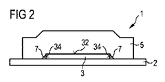
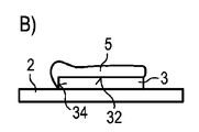
図2による実施例においては、変換手段体5が横方向において半導体積層体3から突出している。この実施例では、半導体積層体3が支持体2上に取り付けられている。半導体積層体3は、支持体2と、変換手段体5と、半導体積層体3との電気的な接触接続のための、図2には図示していない電気的なコンタクト構造とによって完全に包囲されている。半導体積層体3の側面34に中空部7を形成することができる。
In the embodiment according to FIG. 2, the conversion means
変換手段体5の支持体2側とは反対側の境界面は、放射通過面32の上方の領域において、レンズ状の成形部を有している。換言すれば、支持体2を基準にした変換手段体5の高さは横方向における拡張部全体にわたり一定ではない。
The boundary surface of the conversion means
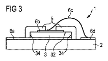
図3による実施例においては、電気的なコンタクト構造6aから6dが示されている。ボンディングワイヤとして形成されているコンタクト構造6cは、半導体積層体3の主延在方向に直交する方向において、ワンピースの変換手段体5を完全に貫通している。
In the embodiment according to FIG. 3,
ここでは、変換手段体5がそれぞれ放射通過面32及び側面34の少なくとも90%を覆っている。電気的なコンタクト構造6bは例えば、半導体積層体3の半導体材料の上に蒸着されている。
Here, the conversion means
図4による実施例においては、コンタクト構造6bが、半導体積層体3上に直接的に取り付けられているワンピースの変換手段体5を完全に貫通している。コンタクト構造6bは例えば蒸着及び/又はフォトリソグラフィプロセスを介して形成されている。コンタクト構造6bも変換手段体5も電気的な絶縁層11によって完全に覆われている。絶縁層5の材料は有利には、変換手段体5のマトリクス材料とは異なる。
In the embodiment according to FIG. 4, the
変換手段体5の硬度はショアD45以上ショアD80以下である。この高い硬度によって、半導体積層体3を変換手段体5によって機械的に保護することができる。更には、高い硬度は特に効率的な噛合部、従って、放射通過面32の構造化部又は粗面部とマトリクス材料50との間の高い固着性を実現する。
The hardness of the conversion means
図5には、半導体積層体3における変換手段体、例えば図1から図4のいずれかによる変換手段体の時間tに依存する剪断力Fが示されている。1000時間の全体の期間にわたり、温度は185℃にある。例えば図1から図4のいずれかによる半導体積層体3からの変換手段体5の層剥離が行なわれる剪断力はそれぞれ少なくとも50Nである。
FIG. 5 shows a shear force F depending on the time t of the conversion means body in the
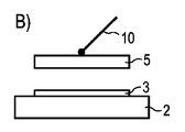
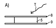
図6には、半導体チップ1に関する製造方法が示されている。図6Aによれば、例えばエチレン−テトラフルオロエチレンフィルムである支持体フィルム8の上に、特にシルクスクリーン法によって、変換手段体5が被着される。続いて、4分間にわたる約150℃の温度での温度作用Tによって、マトリクス材料及び変換手段粒子を有する変換手段体5が硬化される。マトリクス材料は例えば、Shin-Etsu社のLPS−AF500Yである。硬化によって変換手段体はショアA10以上ショアA35以下の硬度を有するので、変換手段体を実装機械(英語Pick and Place Machine)10によって半導体積層体上に取り付けることができる(図6Bを参照されたい)。
FIG. 6 shows a manufacturing method related to the
支持体フィルム8上に形成された変換手段体5を、図6には図示していない任意の別のステップにおいて平滑化して、変換手段体5の非常に均等な厚さを生じさせることができる、及び/又は、変換手段体5を横方向の寸法で切断することができる。この場合には図6Aに示されている実施例とは異なり、支持体フィルム8を横方向において半導体基体5と面一に終端させることも可能である。
The conversion means
続く図6Cにおいては、温度作用Tを介してマトリクス材料が完全に硬化される、及び/又は、架橋されることが示されている。硬化時間は有利には少なくとも10分である。例えば、硬化は150℃の温度で1時間にわたり行なわれる。選択的に、変換手段体5の熱硬化を行なっている時間の全体又は一部にわたり、圧力作用pを介して、変換手段体5を半導体積層体3に押し付けることができる、及び/又は、圧着することができる。
In the subsequent FIG. 6C, it is shown that the matrix material is fully cured and / or cross-linked via temperature action T. The curing time is advantageously at least 10 minutes. For example, curing is performed at a temperature of 150 ° C. for 1 hour. Optionally, the conversion means
図7による方法においては、支持体フィルム8とカバーフィルム9との間に変換手段体5が設けられている(図7Aを参照されたい)。変換手段体5の硬化は、例えば、温度作用Tを介して、及び/又は、支持体フィルム8を通過する紫外線放射又は青色光放射を介して行なわれる。硬化後に、変換手段体5は低い硬度しか有していない、及び/又は、10Pa・s以上70Pa・s以下の比較的低い粘度しか有していない。変換手段体5は例えば圧延によって成形され、また任意に、後続の個別化及び/又は切断が行なわれる。特に変換手段体5がレンズ状に形成される場合には、スタンピング又は圧縮成型も可能である。
In the method according to FIG. 7, a conversion means
図7Bによれば、硬化後にカバーフィルム9が変換手段体5から除去される。変換手段体5は支持体フィルム8上に残存している。
According to FIG. 7B, the
図7Cには、支持体フィルム8を介して変換手段体5が半導体積層体3に被着されることが示されている。ワンピースの変換手段体5の温度作用Tを介する硬化又は光化学的な硬化は、有利に、それと同時に圧力作用pも介して行なわれる。支持体フィルム8を硬化の際に依然として変換手段体5の上に残存させることができるか、又は、図7Cに示されている実施例とは異なり、完全な硬化及び/又は架橋の前に、例えば、半導体積層体3における変換手段体5の位置決め前又は位置決め直後に、支持体フィルム8を既に変換手段体5から除去することができる。
FIG. 7C shows that the conversion means
支持体フィルム8が硬化の前に既に除去されていなかった場合には、支持体フィルム8は完全な硬化後に変換手段体5から取り外される(図7Dを参照されたい)。
If the
図8には、同様に変換手段体5を有している、従来の半導体構成素子が示されている。図8Aによれば、特にシリコーンを含有している変換手段体5が結合手段4を介して半導体積層体3に被着されている。結合手段4は例えば低粘度のシリコーン接着剤である。変換手段体5とは異なり、結合手段4は、動作時に半導体積層体3が放射を生成するスペクトル領域においては透過性であるか透明である。
FIG. 8 shows a conventional semiconductor component having a conversion means
結合手段4が取り付けの際に低い粘度しか有していないことによって、変換手段体5を取り付けた際に、横方向においては、結合手段4が半導体積層体3の側面34、また場合によっては支持体2も部分的に湿潤させる可能性がある。その種の湿潤は、支持体2乃至半導体積層体3の特別な設計、並びに、支持体2の特別な洗浄ステップによって回避することができる。もっともその種の措置によって製造コストは高まる。例えば図1から図4に従い、変換手段体5が結合手段を介さずに取り付けられることによって、結合手段4による例えば支持体2の汚染の危険は存在せず、また、支持体2及び/又は半導体積層体3の煩雑な設計を省略することができる。
Since the coupling means 4 has only a low viscosity at the time of attachment, when the conversion means
図8Bによれば、変換手段体5がシルクスクリーン法によって半導体積層体3上に直接的に被着されている。その種の方法は高い精度を要求し、また比較的コストが掛かる。変換手段体5を半導体積層体3上に直接的に被着させるために、出発材料、また特に完成した変換手段体5は、比較的低い硬度、特にショアA80又はショアA60を下回る硬度しか有していない。
According to FIG. 8B, the conversion means
半導体積層体3上に直接的にシルクスクリーン法を実施する際の硬度に関する材料制限の他に、変換手段体5の厚さも図1から図4による変換手段体5に比べて不均一に構成されるので、これによって、波長変換された放射の色度座標の局所的な変動が生じる可能性がある。結合手段4を使用する場合と同様に、半導体積層体3上に変換手段体5を直接的に印刷する場合には、変換手段体5の材料によって側面34又は支持体2の汚染が生じる危険が存在する。
In addition to the material restrictions relating to the hardness when the silk screen method is performed directly on the
上記において説明した本発明は、実施例に基づいた上記の説明によって限定されるものではない。むしろ本発明はあらゆる新規の特徴並びにそれらの特徴のあらゆる組み合わせを含むものであり、これには殊に特許請求の範囲に記載した特徴の組み合わせ各々が含まれ、このことはそのような組み合わせ自体が特許請求の範囲あるいは実施例に明示的には記載されていないにしても当てはまる。 The present invention described above is not limited by the above description based on the embodiments. Rather, the invention includes all novel features and combinations of those features, particularly including each of the combinations of features recited in the claims, as such a combination itself. This applies even if not explicitly stated in the claims or the examples.
本願は、ドイツ連邦共和国特許出願第10 2009 040 148.2号の優先権を主張するものであり、その開示内容は参照により本願に含まれるものとする。 This application claims the priority of German Patent Application No. 10 2009 040 148.2, the disclosure of which is hereby incorporated by reference.
Claims (12)
マトリクス材料(50)と、
前記マトリクス材料(50)内に埋め込まれている変換手段粒子(55)とを有しており、
前記マトリクス材料(50)は不完全に硬化及び/又は架橋されており、且つ、
前記変換手段体(5)は室温においてショアA0を上回り且つショアA35以下の硬度、及び/又は、10Pa・s以上150Pa・s以下の粘度を有していることを特徴とする、変換手段体(5)。 In the conversion means body (5) for the optoelectronic semiconductor chip (1),
A matrix material (50);
Conversion means particles (55) embedded in the matrix material (50),
The matrix material (50) is incompletely cured and / or crosslinked, and
The conversion means body (5) has a hardness that is higher than Shore A0 and has a hardness of Shore A35 or less and / or a viscosity of 10 Pa · s to 150 Pa · s at room temperature. 5).
少なくとも一つの活性層を備えている半導体積層体(3)と、
変換手段粒子(55)が埋め込まれているマトリクス材料(50)を含むワンピースの変換手段体(5)とを有しており、
前記変換手段体(5)は前記半導体積層体(3)と直接的に接触しており、結合手段を介することなく前記半導体積層体(3)上に被着されており、
前記変換手段体(5)の硬度は少なくともショアA30且つ最大でショアD80であることを特徴とする、オプトエレクトロニクス半導体チップ(1)。 In the optoelectronic semiconductor chip (1),
A semiconductor stack (3) comprising at least one active layer;
A one-piece conversion means body (5) comprising a matrix material (50) in which the conversion means particles (55) are embedded,
The conversion means body (5) is in direct contact with the semiconductor stacked body (3), and is deposited on the semiconductor stacked body (3) without a coupling means;
The optoelectronic semiconductor chip (1), characterized in that the hardness of the conversion means body (5) is at least Shore A30 and at most Shore D80.
前記変換手段(5)の厚さは20μm以上125μm以下である、請求項6に記載のオプトエレクトロニクス半導体チップ(1)。 The horizontal dimension of the conversion means body (5) is 300 μm or more and 3 mm or less,
The optoelectronic semiconductor chip (1) according to claim 6, wherein the thickness of the conversion means (5) is not less than 20 µm and not more than 125 µm.
少なくとも一つの活性層を備えている半導体積層体(3)を準備するステップと、
変換手段粒子(55)が埋め込まれているマトリクス材料(50)を有しているワンピースの変換手段体(5)を準備するステップであって、前記マトリクス材料(50)は不完全に架橋されており、及び/又は、硬化されており、且つ、前記変換手段体(5)は室温においてショアA0を上回り且つショアA35以下の硬度、及び/又は、10Pa・s以上150Pa・s以下の粘度を有するステップと、
前記半導体積層体(3)の上に前記変換手段体(5)を取り付け、前記半導体積層体(3)と前記変換手段体(5)とを相互に直接的に接触させるステップと、
前記変換手段体(5)を硬化させるステップであって、前記硬化後に前記変換手段体(5)の前記硬度は少なくともショアA30且つ最大でショアD80であるステップとを備えていることを特徴とする、オプトエレクトロニクス半導体チップ(1)の製造方法。 In the manufacturing method of the optoelectronic semiconductor chip (1),
Providing a semiconductor stack (3) comprising at least one active layer;
Providing a one-piece conversion means body (5) having a matrix material (50) in which conversion means particles (55) are embedded, said matrix material (50) being incompletely cross-linked And / or cured, and the conversion means body (5) has a hardness of more than Shore A0 and less than or equal to Shore A35 and / or a viscosity of 10 Pa · s to 150 Pa · s at room temperature. Steps,
Attaching the conversion means body (5) on the semiconductor laminate (3) and bringing the semiconductor laminate (3) and the conversion means body (5) into direct contact with each other;
Curing the converting means body (5), wherein the hardness of the converting means body (5) is at least Shore A30 and at most Shore D80 after the curing. The manufacturing method of an optoelectronic semiconductor chip (1).
少なくとも前記支持体フィルム(8)は紫外線スペクトル領域及び青色スペクトル領域において少なくとも部分的に放射を透過させる、請求項11に記載の方法。 The conversion means body (5) is mounted on a support film (8) and covered with a cover film (9),
12. The method according to claim 11, wherein at least the support film (8) is at least partially transparent for radiation in the ultraviolet spectral region and the blue spectral region.
Applications Claiming Priority (3)
| Application Number | Priority Date | Filing Date | Title |
|---|---|---|---|
| DE102009040148A DE102009040148A1 (en) | 2009-09-04 | 2009-09-04 | Conversion medium body, optoelectronic semiconductor chip and method for producing an optoelectronic semiconductor chip |
| DE102009040148.2 | 2009-09-04 | ||
| PCT/EP2010/061648 WO2011026716A1 (en) | 2009-09-04 | 2010-08-10 | Conversion agent body, optoelectronic semiconductor chip, and method for producing an optoelectronic semiconductor chip |
Publications (2)
| Publication Number | Publication Date |
|---|---|
| JP2013504188A true JP2013504188A (en) | 2013-02-04 |
| JP2013504188A5 JP2013504188A5 (en) | 2013-05-30 |
Family
ID=42983504
Family Applications (1)
| Application Number | Title | Priority Date | Filing Date |
|---|---|---|---|
| JP2012527269A Pending JP2013504188A (en) | 2009-09-04 | 2010-08-10 | Conversion means body, optoelectronic semiconductor chip, and method of manufacturing optoelectronic semiconductor chip |
Country Status (8)
| Country | Link |
|---|---|
| US (1) | US9055655B2 (en) |
| EP (1) | EP2474203B1 (en) |
| JP (1) | JP2013504188A (en) |
| KR (1) | KR20120062725A (en) |
| CN (1) | CN102498751B (en) |
| DE (1) | DE102009040148A1 (en) |
| TW (1) | TWI470839B (en) |
| WO (1) | WO2011026716A1 (en) |
Families Citing this family (8)
| Publication number | Priority date | Publication date | Assignee | Title |
|---|---|---|---|---|
| US20110284866A1 (en) * | 2005-01-11 | 2011-11-24 | Tran Chuong A | Light-emitting diode (led) structure having a wavelength-converting layer and method of producing |
| WO2011105858A2 (en) * | 2010-02-25 | 2011-09-01 | (주)라이타이저코리아 | Light emitting diode and method for manufacturing same |
| DE102010049312B4 (en) | 2010-10-22 | 2023-08-03 | OSRAM Opto Semiconductors Gesellschaft mit beschränkter Haftung | Process for producing a conversion plate and conversion plate |
| EP2980836A1 (en) * | 2013-03-28 | 2016-02-03 | Nitto Denko Corporation | Method for manufacturing optical semiconductor device, system, manufacturing conditions determination device, and manufacturing management device |
| DE102014107473A1 (en) * | 2014-05-27 | 2015-12-03 | Osram Opto Semiconductors Gmbh | Converter element for converting a wavelength, optoelectronic component with converter element and method for producing a converter element |
| US10497838B2 (en) * | 2018-04-12 | 2019-12-03 | Osram Opto Semiconductors Gmbh | Method for producing an optic device, optic device and assembly comprising such an optic device |
| DE102021124691A1 (en) | 2021-09-23 | 2023-03-23 | OSRAM Opto Semiconductors Gesellschaft mit beschränkter Haftung | METHOD FOR MANUFACTURING OPTICAL ELEMENTS, METHOD FOR MANUFACTURING SEMICONDUCTOR RADIATION EMITTING DEVICES, OPTICAL ELEMENT AND SEMICONDUCTOR RADIATION EMITTING DEVICE |
| DE102022122981A1 (en) * | 2022-09-09 | 2024-03-14 | Ams-Osram International Gmbh | Method for producing an optoelectronic component and optoelectronic component |
Citations (8)
| Publication number | Priority date | Publication date | Assignee | Title |
|---|---|---|---|---|
| JP2003142737A (en) * | 2001-08-22 | 2003-05-16 | Nichia Chem Ind Ltd | Light emitting device |
| JP2007019096A (en) * | 2005-07-05 | 2007-01-25 | Toyoda Gosei Co Ltd | Light-emitting device and its manufacturing method |
| JP2007146008A (en) * | 2005-11-28 | 2007-06-14 | Kyocera Corp | Fluorophor and wavelength converter and light-emitting device |
| WO2008104936A2 (en) * | 2007-02-26 | 2008-09-04 | Koninklijke Philips Electronics N.V. | Led with phosphor tile and overmolded phosphor in lens |
| WO2009069671A1 (en) * | 2007-11-29 | 2009-06-04 | Nichia Corporation | Light-emitting device and its manufacturing method |
| JP2009188207A (en) * | 2008-02-06 | 2009-08-20 | Nitto Denko Corp | Resin sheet for sealing optical semiconductor element and optical semiconductor device |
| JP2009530437A (en) * | 2006-03-15 | 2009-08-27 | エルジー イノテック カンパニー リミテッド | Phosphorescent sheet |
| JP2009235368A (en) * | 2007-04-10 | 2009-10-15 | Shin Etsu Chem Co Ltd | Production methods of phosphor-containing adhesive silicone composition, composition sheet composed of the composition and light-emitting apparatus using the sheet |
Family Cites Families (9)
| Publication number | Priority date | Publication date | Assignee | Title |
|---|---|---|---|---|
| US7285913B2 (en) | 2003-08-29 | 2007-10-23 | Matsushita Electric Industrial Co., Ltd. | Plasma display device having blue phosphor layers with alkaline earth metal aluminate containing molybdenum or tungsten |
| US20050211991A1 (en) * | 2004-03-26 | 2005-09-29 | Kyocera Corporation | Light-emitting apparatus and illuminating apparatus |
| CN102800786B (en) | 2006-04-24 | 2015-09-16 | 克利公司 | Light-emitting diode and display element |
| US7923928B2 (en) * | 2006-06-27 | 2011-04-12 | Mitsubishi Chemical Corporation | Illuminating device |
| CN1976069A (en) * | 2006-12-05 | 2007-06-06 | 上海纳晶科技有限公司 | Method for producing white light LED with thermal insulation packaging structure |
| JP5080881B2 (en) * | 2007-06-27 | 2012-11-21 | ナミックス株式会社 | Method for manufacturing sealed body of light emitting diode chip |
| DE102007054800A1 (en) * | 2007-09-28 | 2009-04-02 | Osram Opto Semiconductors Gmbh | Luminescence conversion film for e.g. luminescence diode chip, has luminescence conversion material with fluorescent substance that is in form of organic particles, where film exhibits specific transparency to visible wavelength range |
| WO2009119038A2 (en) | 2008-03-28 | 2009-10-01 | Panasonic Corporation | Molded resin product, semiconductor light-emitting source, lighting device, and method for manufacturing molded resin product |
| CN101333422A (en) | 2008-07-11 | 2008-12-31 | 包书林 | Adhesive for LED chip |
-
2009
- 2009-09-04 DE DE102009040148A patent/DE102009040148A1/en not_active Withdrawn
-
2010
- 2010-08-10 CN CN201080030130.XA patent/CN102498751B/en not_active Expired - Fee Related
- 2010-08-10 KR KR20127004528A patent/KR20120062725A/en not_active Application Discontinuation
- 2010-08-10 EP EP10740673.8A patent/EP2474203B1/en not_active Not-in-force
- 2010-08-10 US US13/377,593 patent/US9055655B2/en not_active Expired - Fee Related
- 2010-08-10 JP JP2012527269A patent/JP2013504188A/en active Pending
- 2010-08-10 WO PCT/EP2010/061648 patent/WO2011026716A1/en active Application Filing
- 2010-09-03 TW TW99129814A patent/TWI470839B/en not_active IP Right Cessation
Patent Citations (8)
| Publication number | Priority date | Publication date | Assignee | Title |
|---|---|---|---|---|
| JP2003142737A (en) * | 2001-08-22 | 2003-05-16 | Nichia Chem Ind Ltd | Light emitting device |
| JP2007019096A (en) * | 2005-07-05 | 2007-01-25 | Toyoda Gosei Co Ltd | Light-emitting device and its manufacturing method |
| JP2007146008A (en) * | 2005-11-28 | 2007-06-14 | Kyocera Corp | Fluorophor and wavelength converter and light-emitting device |
| JP2009530437A (en) * | 2006-03-15 | 2009-08-27 | エルジー イノテック カンパニー リミテッド | Phosphorescent sheet |
| WO2008104936A2 (en) * | 2007-02-26 | 2008-09-04 | Koninklijke Philips Electronics N.V. | Led with phosphor tile and overmolded phosphor in lens |
| JP2009235368A (en) * | 2007-04-10 | 2009-10-15 | Shin Etsu Chem Co Ltd | Production methods of phosphor-containing adhesive silicone composition, composition sheet composed of the composition and light-emitting apparatus using the sheet |
| WO2009069671A1 (en) * | 2007-11-29 | 2009-06-04 | Nichia Corporation | Light-emitting device and its manufacturing method |
| JP2009188207A (en) * | 2008-02-06 | 2009-08-20 | Nitto Denko Corp | Resin sheet for sealing optical semiconductor element and optical semiconductor device |
Also Published As
| Publication number | Publication date |
|---|---|
| TW201117432A (en) | 2011-05-16 |
| KR20120062725A (en) | 2012-06-14 |
| EP2474203A1 (en) | 2012-07-11 |
| EP2474203B1 (en) | 2017-08-02 |
| CN102498751A (en) | 2012-06-13 |
| WO2011026716A1 (en) | 2011-03-10 |
| CN102498751B (en) | 2016-05-18 |
| DE102009040148A1 (en) | 2011-03-10 |
| TWI470839B (en) | 2015-01-21 |
| US9055655B2 (en) | 2015-06-09 |
| US20120146076A1 (en) | 2012-06-14 |
Similar Documents
| Publication | Publication Date | Title |
|---|---|---|
| JP2013504188A (en) | Conversion means body, optoelectronic semiconductor chip, and method of manufacturing optoelectronic semiconductor chip | |
| JP5721823B2 (en) | Device and device manufacturing method | |
| US10205067B2 (en) | LED with ceramic green phosphor and protected red phosphor layer | |
| JP3685018B2 (en) | Light emitting device and manufacturing method thereof | |
| TWI316747B (en) | Surface mountable optoelectronic component and its production method | |
| JP6129322B2 (en) | Semiconductor light emitting device and optical film | |
| TWI544662B (en) | Semiconductor device and production method therefor | |
| TWI422069B (en) | Semiconductor device and production method therefor | |
| JP6668608B2 (en) | Light emitting device manufacturing method | |
| WO2013137356A1 (en) | Semiconductor light emitting device and method for manufacturing same | |
| US20100171215A1 (en) | Method of Producing Optoelectronic Components and Optoelectronic Component | |
| TW201635594A (en) | Light emitting device and its manufacturing method | |
| TW200541110A (en) | Semiconductor light emitting devices including flexible film having therein an optical element, and methods of assembling same | |
| JP2009537970A (en) | Electrically conductive connection using an insulating connection medium | |
| US20180033925A1 (en) | Method of producing a light-emitting device, and light-emitting device | |
| JP6447018B2 (en) | LIGHT EMITTING DEVICE AND LIGHT EMITTING DEVICE MANUFACTURING METHOD | |
| JP5896214B2 (en) | Manufacturing method of semiconductor device | |
| JP5882910B2 (en) | Package and manufacturing method thereof | |
| TW200822353A (en) | Light emitting diode assembly and method of fabrication | |
| JP6760356B2 (en) | Light emitting device and manufacturing method of light emitting device | |
| JP5721894B2 (en) | Optical semiconductor device | |
| JP2018120947A (en) | Method for manufacturing optical semiconductor element with functional layer-coating layer | |
| KR101450216B1 (en) | Method of manufacutruing semiconductor device structure | |
| JP4367299B2 (en) | LIGHT EMITTING DEVICE AND LIGHT EMITTING DEVICE DEVICE MANUFACTURING METHOD | |
| KR102051478B1 (en) | Semiconductor light emitting device and method of manufacturing the same |
Legal Events
| Date | Code | Title | Description |
|---|---|---|---|
| A521 | Request for written amendment filed |
Free format text: JAPANESE INTERMEDIATE CODE: A523 Effective date: 20130415 |
|
| A621 | Written request for application examination |
Free format text: JAPANESE INTERMEDIATE CODE: A621 Effective date: 20130415 |
|
| A977 | Report on retrieval |
Free format text: JAPANESE INTERMEDIATE CODE: A971007 Effective date: 20140124 |
|
| A131 | Notification of reasons for refusal |
Free format text: JAPANESE INTERMEDIATE CODE: A131 Effective date: 20140203 |
|
| A601 | Written request for extension of time |
Free format text: JAPANESE INTERMEDIATE CODE: A601 Effective date: 20140418 |
|
| A602 | Written permission of extension of time |
Free format text: JAPANESE INTERMEDIATE CODE: A602 Effective date: 20140425 |
|
| A521 | Request for written amendment filed |
Free format text: JAPANESE INTERMEDIATE CODE: A523 Effective date: 20140725 |
|
| A02 | Decision of refusal |
Free format text: JAPANESE INTERMEDIATE CODE: A02 Effective date: 20141215 |