JP2013503259A - Ion plasma electron emitter for melting furnace - Google Patents
Ion plasma electron emitter for melting furnace Download PDFInfo
- Publication number
- JP2013503259A JP2013503259A JP2012526811A JP2012526811A JP2013503259A JP 2013503259 A JP2013503259 A JP 2013503259A JP 2012526811 A JP2012526811 A JP 2012526811A JP 2012526811 A JP2012526811 A JP 2012526811A JP 2013503259 A JP2013503259 A JP 2013503259A
- Authority
- JP
- Japan
- Prior art keywords
- electron
- field
- cathode
- ion plasma
- melting
- Prior art date
- Legal status (The legal status is an assumption and is not a legal conclusion. Google has not performed a legal analysis and makes no representation as to the accuracy of the status listed.)
- Pending
Links
Images


Classifications
-
- B—PERFORMING OPERATIONS; TRANSPORTING
- B22—CASTING; POWDER METALLURGY
- B22D—CASTING OF METALS; CASTING OF OTHER SUBSTANCES BY THE SAME PROCESSES OR DEVICES
- B22D11/00—Continuous casting of metals, i.e. casting in indefinite lengths
- B22D11/10—Supplying or treating molten metal
- B22D11/11—Treating the molten metal
-
- C—CHEMISTRY; METALLURGY
- C22—METALLURGY; FERROUS OR NON-FERROUS ALLOYS; TREATMENT OF ALLOYS OR NON-FERROUS METALS
- C22B—PRODUCTION AND REFINING OF METALS; PRETREATMENT OF RAW MATERIALS
- C22B4/00—Electrothermal treatment of ores or metallurgical products for obtaining metals or alloys
- C22B4/005—Electrothermal treatment of ores or metallurgical products for obtaining metals or alloys using plasma jets
-
- H—ELECTRICITY
- H01—ELECTRIC ELEMENTS
- H01J—ELECTRIC DISCHARGE TUBES OR DISCHARGE LAMPS
- H01J37/00—Discharge tubes with provision for introducing objects or material to be exposed to the discharge, e.g. for the purpose of examination or processing thereof
- H01J37/30—Electron-beam or ion-beam tubes for localised treatment of objects
- H01J37/305—Electron-beam or ion-beam tubes for localised treatment of objects for casting, melting, evaporating or etching
-
- C—CHEMISTRY; METALLURGY
- C22—METALLURGY; FERROUS OR NON-FERROUS ALLOYS; TREATMENT OF ALLOYS OR NON-FERROUS METALS
- C22B—PRODUCTION AND REFINING OF METALS; PRETREATMENT OF RAW MATERIALS
- C22B9/00—General processes of refining or remelting of metals; Apparatus for electroslag or arc remelting of metals
- C22B9/04—Refining by applying a vacuum
-
- C—CHEMISTRY; METALLURGY
- C22—METALLURGY; FERROUS OR NON-FERROUS ALLOYS; TREATMENT OF ALLOYS OR NON-FERROUS METALS
- C22B—PRODUCTION AND REFINING OF METALS; PRETREATMENT OF RAW MATERIALS
- C22B9/00—General processes of refining or remelting of metals; Apparatus for electroslag or arc remelting of metals
- C22B9/16—Remelting metals
- C22B9/22—Remelting metals with heating by wave energy or particle radiation
- C22B9/228—Remelting metals with heating by wave energy or particle radiation by particle radiation, e.g. electron beams
-
- F—MECHANICAL ENGINEERING; LIGHTING; HEATING; WEAPONS; BLASTING
- F27—FURNACES; KILNS; OVENS; RETORTS
- F27B—FURNACES, KILNS, OVENS, OR RETORTS IN GENERAL; OPEN SINTERING OR LIKE APPARATUS
- F27B3/00—Hearth-type furnaces, e.g. of reverberatory type; Tank furnaces
- F27B3/08—Hearth-type furnaces, e.g. of reverberatory type; Tank furnaces heated electrically, with or without any other source of heat
-
- F—MECHANICAL ENGINEERING; LIGHTING; HEATING; WEAPONS; BLASTING
- F27—FURNACES; KILNS; OVENS; RETORTS
- F27B—FURNACES, KILNS, OVENS, OR RETORTS IN GENERAL; OPEN SINTERING OR LIKE APPARATUS
- F27B3/00—Hearth-type furnaces, e.g. of reverberatory type; Tank furnaces
- F27B3/10—Details, accessories, or equipment peculiar to hearth-type furnaces
- F27B3/20—Arrangements of heating devices
-
- F—MECHANICAL ENGINEERING; LIGHTING; HEATING; WEAPONS; BLASTING
- F27—FURNACES; KILNS; OVENS; RETORTS
- F27B—FURNACES, KILNS, OVENS, OR RETORTS IN GENERAL; OPEN SINTERING OR LIKE APPARATUS
- F27B5/00—Muffle furnaces; Retort furnaces; Other furnaces in which the charge is held completely isolated
- F27B5/04—Muffle furnaces; Retort furnaces; Other furnaces in which the charge is held completely isolated adapted for treating the charge in vacuum or special atmosphere
-
- F—MECHANICAL ENGINEERING; LIGHTING; HEATING; WEAPONS; BLASTING
- F27—FURNACES; KILNS; OVENS; RETORTS
- F27D—DETAILS OR ACCESSORIES OF FURNACES, KILNS, OVENS, OR RETORTS, IN SO FAR AS THEY ARE OF KINDS OCCURRING IN MORE THAN ONE KIND OF FURNACE
- F27D99/00—Subject matter not provided for in other groups of this subclass
- F27D99/0001—Heating elements or systems
- F27D99/0006—Electric heating elements or system
-
- H—ELECTRICITY
- H01—ELECTRIC ELEMENTS
- H01J—ELECTRIC DISCHARGE TUBES OR DISCHARGE LAMPS
- H01J37/00—Discharge tubes with provision for introducing objects or material to be exposed to the discharge, e.g. for the purpose of examination or processing thereof
- H01J37/02—Details
- H01J37/04—Arrangements of electrodes and associated parts for generating or controlling the discharge, e.g. electron-optical arrangement, ion-optical arrangement
- H01J37/06—Electron sources; Electron guns
- H01J37/077—Electron guns using discharge in gases or vapours as electron sources
-
- C—CHEMISTRY; METALLURGY
- C22—METALLURGY; FERROUS OR NON-FERROUS ALLOYS; TREATMENT OF ALLOYS OR NON-FERROUS METALS
- C22B—PRODUCTION AND REFINING OF METALS; PRETREATMENT OF RAW MATERIALS
- C22B9/00—General processes of refining or remelting of metals; Apparatus for electroslag or arc remelting of metals
- C22B9/16—Remelting metals
- C22B9/22—Remelting metals with heating by wave energy or particle radiation
- C22B9/226—Remelting metals with heating by wave energy or particle radiation by electric discharge, e.g. plasma
-
- H—ELECTRICITY
- H01—ELECTRIC ELEMENTS
- H01J—ELECTRIC DISCHARGE TUBES OR DISCHARGE LAMPS
- H01J2237/00—Discharge tubes exposing object to beam, e.g. for analysis treatment, etching, imaging
- H01J2237/15—Means for deflecting or directing discharge
-
- H—ELECTRICITY
- H01—ELECTRIC ELEMENTS
- H01J—ELECTRIC DISCHARGE TUBES OR DISCHARGE LAMPS
- H01J2237/00—Discharge tubes exposing object to beam, e.g. for analysis treatment, etching, imaging
- H01J2237/30—Electron or ion beam tubes for processing objects
- H01J2237/31—Processing objects on a macro-scale
- H01J2237/3128—Melting
Landscapes
- Engineering & Computer Science (AREA)
- Chemical & Material Sciences (AREA)
- Mechanical Engineering (AREA)
- General Engineering & Computer Science (AREA)
- Physics & Mathematics (AREA)
- Plasma & Fusion (AREA)
- Materials Engineering (AREA)
- Manufacturing & Machinery (AREA)
- Metallurgy (AREA)
- Organic Chemistry (AREA)
- Analytical Chemistry (AREA)
- Health & Medical Sciences (AREA)
- Toxicology (AREA)
- Life Sciences & Earth Sciences (AREA)
- Environmental & Geological Engineering (AREA)
- General Life Sciences & Earth Sciences (AREA)
- Geochemistry & Mineralogy (AREA)
- Geology (AREA)
- Manufacture And Refinement Of Metals (AREA)
- Furnace Details (AREA)
- Discharge Heating (AREA)
- Continuous Casting (AREA)
Abstract
導電性の金属材料を溶融させる装置は、第一の形状を有する断面外形を含む収束した電子フィールドを作り出す構成とされた補助イオンプラズマ電子エミッタを備えている。該装置は、収束した電子フィールドを導電性の金属材料の少なくとも一部分に衝突させ、導電性の金属材料の任意の凝固部分、導電性の金属材料中の任意の固体の凝縮体及び/又は凝固するインゴットの領域の溶融又は加熱の少なくとも1つを行う構成とされたステアリングシステムを備えている。
【選択図】図1An apparatus for melting a conductive metallic material includes an auxiliary ion plasma electron emitter configured to create a focused electron field including a cross-sectional profile having a first shape. The apparatus impinges the focused electron field on at least a portion of the conductive metal material to solidify any solidified portion of the conductive metal material, any solid condensate and / or solidify in the conductive metal material. A steering system is provided that is configured to perform at least one of melting or heating the region of the ingot.
[Selection] Figure 1
Description
[0001] 本出願は、米国法35U.S.C第120に基づく優先権を主張し、且つ2007年3月30日付けで出願した米国仮特許出願第第60/909,118号に対して米国法35U.S.C第119に基づく優先権を主張する、2008年3月26日付けで出願した、米国特許出願第12/055,415号の一部継続出願である。上記の先の出願の双方は、その内容の全体を参考として引用し本明細書に含めてある。 [0001] This application is subject to United States Act 35U. S. US Provisional Patent Application No. 60 / 909,118 claiming priority under C.120 and filed on March 30, 2007 is subject to US law 35U. S. This is a continuation-in-part of US patent application Ser. No. 12 / 055,415, filed Mar. 26, 2008, claiming priority under C-119. Both of the aforementioned earlier applications are incorporated herein by reference in their entirety.
[0002] 本発明は、金属及び金属合金(以下、「合金」という)を溶融させる装置及び技術に関する。本発明は、より特定的には、電子を利用して、合金を及び(又は)溶融した合金中に形成された凝縮物を溶融させ又は加熱する装置及び技術に関するものである。 The present invention relates to an apparatus and a technique for melting a metal and a metal alloy (hereinafter referred to as “alloy”). More particularly, the present invention relates to an apparatus and technique for utilizing an electron to melt or heat an alloy and / or condensate formed in a molten alloy.
[0003] 合金の溶融方法は、適当な材料の装入物を製造し、次に、その装入物を溶融させる工程を含む。次に、その溶融した装入物、すなわち「溶融体」を精製し、且つ(又は)処理して、溶融体の化学的性質を改質し、溶融体から望ましくない成分を除去し、且つ(又は)溶融体から鋳造した物品の微細構造に影響を与えることができる。溶融炉は電気又は化石燃料の燃焼の何れかによって運転し、また、適当な装置の選択は、製造される材料の型式のみならず、相対的なコスト及び適用される環境上の規制によって大きく左右される。今日、多様な溶融技術及び装置が利用可能である。一般的な型式の溶融技術は、例えば、誘導溶融(真空誘導溶融を含む)、アーク溶融(真空アークスカル溶融を含む)、るつぼ溶融、及び電子ビーム溶融を含む。 [0003] A method for melting an alloy includes the steps of producing a charge of a suitable material and then melting the charge. The molten charge, or “melt”, is then purified and / or processed to modify the chemistry of the melt, remove unwanted components from the melt, and ( Or) it can affect the microstructure of articles cast from the melt. The melting furnace is operated either by electricity or fossil fuel combustion, and the selection of the appropriate equipment depends largely on the relative cost and applicable environmental regulations as well as the type of material being produced. Is done. Today, a variety of melting techniques and equipment are available. Common types of melting techniques include, for example, induction melting (including vacuum induction melting), arc melting (including vacuum arc skull melting), crucible melting, and electron beam melting.
[0004] 電子ビーム溶融法は、通常、熱イオン電子ビーム銃を利用して、高エネルギの実質的に線形の電子流れを発生させ、この電子流れを使用して標的の材料を加熱する。熱イオン電子ビーム銃は、電流をフィラメントまで流することにより作動し、これによりフィラメントを高温度まで加熱し、電子を「沸騰」させてフィラメントから分離させる。次に、フィラメントから発生された電子を収束させ、且つ極めて狭小な、実質的に線形の電子ビームの形態にて標的に向けて加速させる。1つの型式のイオンプラズマ電子ビーム銃は合金溶融体を製造するためにも使用されている。特定的には、1994年の電子ビーム溶融に関する国際会議(ネバダ州、レノ)、259−267ページにおけるV.A.シェルノフ(Chernov)による「強力な高電圧グロー放電電子銃及びその基部のパワーユニット(Powerful High−Voltage Glow Discharge Electron Gun and Power Unit on its Base)、に記載された「グロー放電(glow discharge)」電子ビーム銃は、ウクライナ、キエフのアンタレス(Antares)から入手可能な特定の溶融炉に組み込まれている。かかる装置は、カチオンを含む冷間プラズマを作り出すことにより作動し、そのカチオンは、カソードにぶつかり、電子を作り出し、この電子を収束させて、実質的に線形の電子ビームを形成する。 [0004] Electron beam melting typically utilizes a thermionic electron beam gun to generate a high energy, substantially linear electron flow that is used to heat the target material. A thermionic electron beam gun operates by passing a current through the filament, which heats the filament to a high temperature, causing the electrons to “boil” and separate from the filament. The electrons generated from the filament are then focused and accelerated towards the target in the form of a very narrow, substantially linear electron beam. One type of ion plasma electron beam gun has also been used to produce alloy melts. Specifically, the 1994 International Conference on Electron Beam Melting (Reno, NV), pages 259-267. A. “Glow discharge (glow beam)” described in “Powerful High-Voltage Glow Discharge Electron Gun and Power Units on it Base” by Chernov. The gun is incorporated into a specific melting furnace available from Antares, Kiev, Ukraine. Such an apparatus operates by creating a cold plasma containing cations that strike the cathode, create electrons, and focus the electrons to form a substantially linear electron beam.
[0005] 上記型式の電子ビーム銃によって作り出された実質的に線形の電子ビームは、電子ビーム溶融炉の真空溶融室内に向けられ、且つ溶融すべき且つ溶融状態に維持すべき材料に衝突させる。電子を導電性材料を通して伝導することはその材料を急速に、特定の溶融温度以上の温度まで加熱することになる。例えば、約100kW/cm2となる実質的に線形の電子ビームの高エネルギを考えるならば、線形の電子ビーム銃は、極めて高温度の熱源であり、実質的に線形のビームが衝突する材料の溶融温度、また、場合によっては、その気化温度を容易に上回る可能性がある。磁気偏向又は類似の方向決め手段を使用すれば、実質的に線形の電子ビームを溶融室内にて標的の材料を渡って高周波数にてラスター走査し、ビームを広い面積を渡り、且つ多数の複雑な形状を有する標的を渡って向けることが可能である。 [0005] A substantially linear electron beam produced by an electron beam gun of the above type is directed into a vacuum melting chamber of an electron beam melting furnace and impinges on a material to be melted and maintained in a molten state. Conducting electrons through a conductive material rapidly heats the material to a temperature above a certain melting temperature. For example, considering the high energy of a substantially linear electron beam, which is about 100 kW / cm 2 , the linear electron beam gun is a very high temperature heat source, and the material of the material that the substantially linear beam collides with. It can easily exceed the melting temperature and, in some cases, its vaporization temperature. Using magnetic deflection or similar directing means, a substantially linear electron beam can be raster scanned at high frequencies across the target material in the melt chamber, the beam spans a large area, and many complex It is possible to aim across a target having a different shape.
[0006] 電子ビーム溶融法は表面加熱法であるため、この方法は、通常、浅い溶融プールしか作り出さず、このことは、鋳造したインゴットの多孔質巣及び偏析を少なくする点にて有益である。電子ビームにより作り出された過熱した金属プールは、炉の溶融室の高い真空環境内に配置されるため、この技術は、溶融材料のガス抜きをする傾向となる点にても有益である。また、相対的に高い蒸気圧力を有する合金内の望ましくない金属及び非金属組成物は、溶融室内にて選択的に気化させ、これにより合金の純度を向上させることができる。他方、高度に収束させた実質的に線形の電子ビームにより作り出された望ましい組成物の気化について考慮しなければならない。望ましくない気化は製造時のファクタとしなければならず、また、電子ビーム溶融炉を使用するとき、合金の製造を著しく複雑にするであろう。 [0006] Since the electron beam melting method is a surface heating method, this method typically produces only a shallow molten pool, which is beneficial in reducing the porosity and segregation of the cast ingot. . This technique is also beneficial in that it tends to vent the molten material because the superheated metal pool created by the electron beam is placed in the high vacuum environment of the furnace melting chamber. Also, undesirable metal and non-metal compositions within the alloy having relatively high vapor pressure can be selectively vaporized in the melting chamber, thereby improving the purity of the alloy. On the other hand, the vaporization of the desired composition produced by a highly focused, substantially linear electron beam must be considered. Undesirable vaporization must be a manufacturing factor and will significantly complicate alloy production when using an electron beam melting furnace.
[0007] 色々な溶融及び精製方法は、熱イオン電子銃を使用して供給材料を電子ビームにて溶融させる工程を含む。滴下(Drip)溶融法は、例えば、タンタル及びニオブのような耐火性金属を加工するため熱イオン電子ビーム銃溶融炉にて使用される古典的方法である。通常、バーの形態をした原材料は、炉室内に供給され、且つバーにて収束させた線形の電子ビームは、材料を直接、固定鋳型及び又は引抜き鋳型に滴下溶融させる。引抜き鋳型内にて鋳造するとき、インゴットの底部を引抜くことにより、成長するインゴットの頂部に液体プールレベルが維持される。上述したガス抜き及び選択的な気化現象の結果、供給材料は精製される。 [0007] Various melting and purification methods include the step of melting the feed with an electron beam using a thermionic electron gun. The drop melting method is a classic method used in hot ion electron beam gun melting furnaces to process refractory metals such as tantalum and niobium, for example. Usually, a raw material in the form of a bar is fed into the furnace chamber and a linear electron beam focused in the bar drops the material directly into a fixed mold and / or a drawing mold. When casting in a drawing mold, the liquid pool level is maintained at the top of the growing ingot by drawing the bottom of the ingot. As a result of the degassing and selective vaporization described above, the feedstock is purified.
[0008] 電子ビーム冷間炉床溶融技術(electron beam coldhearth melting technique)は、一般に反応性金属及び合金の加工及び再利用工程にて使用される。供給材料は、実質的に線形の電子ビームを供給材料バーの一端に衝突させることにより、滴下溶融させる。溶融した供給材料は、水冷式銅炉床の一端領域内に滴下し、保護スカルを形成する。溶融材料が炉床内に集まると、この材料は溢れ出て、且つ重力によって引抜き鋳型又はその他の鋳造装置内に落下する。炉床内での溶融材料の休止時間中、実質的に線形の電子ビームは、急速に、材料の表面を渡ってラスター走査され、その材料を溶融形態に保持する。このことは、また、高い蒸気圧力の成分の気化を通じて溶融材料をガス抜きし且つ精製する効果を有する。また、炉床は、高密度及び低密度の固体介入物の重力による分離を促進する寸法とすることもでき、その場合、酸化物及びその他の相対的に低密度の介入物は、解離を許容するのに十分な時間溶融金属内に止まる一方、高密度の粒子は底部に沈着し、且つスカル内に取り込まれる。 [0008] Electron beam cold heart melting technique is commonly used in processing and recycling processes for reactive metals and alloys. The feed material is dripped and melted by impinging a substantially linear electron beam on one end of the feed material bar. The molten feed material is dropped into one end region of the water-cooled copper hearth to form a protective skull. As the molten material collects in the hearth, it overflows and falls into the drawing mold or other casting apparatus by gravity. During the downtime of the molten material in the hearth, the substantially linear electron beam is rapidly rastered across the surface of the material to hold the material in the molten form. This also has the effect of degassing and purifying the molten material through vaporization of high vapor pressure components. The hearth can also be dimensioned to facilitate gravity separation of high density and low density solid inclusions, in which case oxides and other relatively low density inclusions are allowed to dissociate. While remaining in the molten metal for a time sufficient to do so, the dense particles are deposited at the bottom and entrained in the skull.
[0009] 従来の電子ビーム溶融技術の色々な利点を考えるならば、この技術を更に改良することは更に有益であろう。 [0000] Considering the various advantages of conventional electron beam melting techniques, it would be further beneficial to further improve this technique.
[0010] 本発明の1つの非限定的な特徴に従い、導電性の金属材料を溶融させる装置が記載されている。該装置は、真空室と、真空室内に配置された炉床と、真空室内に又は真空室に隣接して配置され、且つ第一の断面積を有する第一の電子フィールドを真空室内に向けるよう位置決めされた少なくとも1つのイオンプラズ電子エミッタとを備えている。第一の電子フィールドは、導電性の金属材料をその溶融温度まで加熱するのに十分なエネルギを有している。該装置は、少なくとも1つの鋳型と、炉床から導電性の金属材料を受け取るよう位置決めされた噴霧装置と、真空室内に又は真空室内に隣接して配置され、且つ、第二の断面積を有する第二の電子フィールドを真空室内に向けるよう位置決めされた補助イオンプラズマ電子エミッタとを更に備えている。第二の電子フィールドは、導電性の金属材料の加熱部分をその溶融温度まで加熱し、導電性の金属材料中の任意の固体の凝縮物を溶融させ、且つ形成するインゴットの領域に熱を提供する小鳥少なくとも1つを行うのに十分なエネルギを有している。第一の電子フィールドの第一の断面積は、第二の電子フィールドの第二の断面積と相違している。補助イオンプラズマ電子エミッタにより放出された第二の電子フィールドはステア可能である。 [0010] In accordance with one non-limiting feature of the present invention, an apparatus for melting a conductive metallic material is described. The apparatus directs a vacuum chamber, a hearth disposed in the vacuum chamber, and a first electronic field disposed in or adjacent to the vacuum chamber and having a first cross-sectional area into the vacuum chamber. And at least one ion-plasma electron emitter positioned. The first electronic field has sufficient energy to heat the conductive metal material to its melting temperature. The apparatus includes at least one mold, a spray apparatus positioned to receive conductive metal material from the hearth, and is disposed in or adjacent to the vacuum chamber and has a second cross-sectional area. An auxiliary ion plasma electron emitter positioned to direct the second electron field into the vacuum chamber. The second electronic field heats the heated portion of the conductive metal material to its melting temperature, melts any solid condensate in the conductive metal material, and provides heat to the area of the ingot that forms Have enough energy to do at least one small bird. The first cross-sectional area of the first electron field is different from the second cross-sectional area of the second electron field. The second electron field emitted by the auxiliary ion plasma electron emitter can be steered.
[0011] 本発明の別の非限定的な実施の形態に従い、導電性の金属材料を溶融させる装置が記載されている。該装置は、真空室と、真空室内に配置された炉床と、導電性の金属材料を溶融させる構成とされた溶融装置とを備えている。該装置は、少なくとも1つの鋳型と、炉床から溶融した導電性の金属材料を受け取るよう位置決めされた噴霧装置と、真空室内に又は真空室に隣接して配置され、且つある断面積を有する収束した電子フィールドを真空室内に向けるよう位置決めされた補助イオンプラズマ電子エミッタとを更に備えている。収束した電子フィールドは、導電性の金属材料の一部分を溶融させ、導電性の金属材料中の固体の凝縮物を溶融させ、且つ凝固するインゴットの領域を加熱することの少なくとも1つを行うのに十分なエネルギを有している。収束した電子フィールドをステアして、収束した電子フィールドを導電性の金属材料、固体の凝縮物、及び凝固するインゴットの少なくとも一部分に向けることができる。 [0011] In accordance with another non-limiting embodiment of the present invention, an apparatus for melting a conductive metallic material is described. The apparatus includes a vacuum chamber, a hearth disposed in the vacuum chamber, and a melting device configured to melt a conductive metal material. The apparatus includes at least one mold, a spray device positioned to receive molten conductive metallic material from the hearth, and a convergence disposed in or adjacent to the vacuum chamber and having a cross-sectional area. And an auxiliary ion plasma electron emitter positioned to direct the electron field into the vacuum chamber. The focused electron field is used to melt at least one of melting a portion of the conductive metal material, melting a solid condensate in the conductive metal material, and heating the solidified ingot region. It has enough energy. The focused electron field can be steered to direct the focused electron field to at least a portion of the conductive metallic material, the solid condensate, and the solidifying ingot.
[0012] 本発明の更に別の非限定的な特徴に従い、導電性の金属材料を溶融させる装置が記載されている。該装置は、第一の形状を有する断面外形を含む収束した電子フィールドを作り出す構成とされた補助イオンプラズマ電子エミッタを備えている。該装置は、収束した電子ビームを向けて導電性の金属材料の少なくとも一部分上にて収束した電子フィールドに衝突し、導電性の金属材料の任意の凝固部分を溶融させ、導電性の金属材料中の任意の固体の凝縮物を溶融させ、及び形成するインゴットの領域を加熱することの少なくとも1つを行なう構成とされたステアリングシステムを更に備えている。 [0012] In accordance with yet another non-limiting feature of the present invention, an apparatus for melting a conductive metal material is described. The apparatus includes an auxiliary ion plasma electron emitter configured to produce a focused electron field including a cross-sectional profile having a first shape. The apparatus directs a focused electron beam to impinge on a focused electron field on at least a portion of the conductive metallic material, melting any solidified portion of the conductive metallic material, and in the conductive metallic material. A steering system configured to perform at least one of melting any solid condensate and heating a region of the ingot to form.
[0013] 本発明の更なる特徴に従い、ある材料を加工する方法が提供される。該方法は、金属及び金属合金の少なくとも一方を含む材料を雰囲気圧力に対して低圧力に維持された炉室内に導入するステップと、少なくとも第一のイオンプラズマ電子エミッタを使用して第一の断面積を有する第一の電子フィールドを発生させるステップとを備えている。該方法は、炉室内の材料に対し第一の電子フィールドを作用させ、材料を該材料の溶融温度よりも高い温度まで加熱するステップと、第二のイオンプラズマ電子エミッタを使用して、第二の断面積を有する第二の電子フィールドを発生させるステップとを更に備えている。該方法は、材料中の任意の固体の凝縮物、材料の任意の凝固部分、及び凝固するインゴットの領域の少なくとも一方に対し、ステアシステムを使用して第二の電子フィールドを作用させ、固体の凝縮物、凝固部分及び凝固するインゴットの領域の少なくとも1つを溶融させ又は加熱するステップを更に備えている。第一の電子フィールドの第一の断面積は、第二の電子フィールドの第二の断面積と相違する。 [0013] According to a further feature of the present invention, a method of processing a material is provided. The method includes introducing a material including at least one of a metal and a metal alloy into a furnace chamber maintained at a low pressure relative to an atmospheric pressure, and using a first ion plasma electron emitter for a first disconnection. Generating a first electronic field having an area. The method includes applying a first electron field to the material in the furnace chamber, heating the material to a temperature above the melting temperature of the material, and using a second ion plasma electron emitter, Generating a second electron field having a cross-sectional area of The method uses a steer system to act on a second electronic field on at least one of any solid condensate in the material, any solidified portion of the material, and a region of the ingot to solidify, and the solid The method further comprises melting or heating at least one of the condensate, the solidified portion and the region of the ingot to solidify. The first cross-sectional area of the first electron field is different from the second cross-sectional area of the second electron field.
[0014] 本発明の更なる特徴に従い、ある材料を加工する方法が提供される。該方法は、金属及び金属合金の少なくとも一方を含む材料を雰囲気圧力に対して低い圧力に維持された炉室内に導入するステップと、炉室内の材料に対し、材料をその材料の溶融温度よりも高い温度まで加熱する構成とされた溶融装置を作用させるステップとを備えている。該方法は、補助イオンプラズマ電子エミッタを使用して収束した電子フィールドを発生させるステップと、材料中の任意の固体の凝縮物、材料の任意の凝固部分、及び凝固するインゴットの領域の少なくとも1つに対し、ステアリングシステムを使用して収束した電子フィールドを作用させ、固体の凝縮物、凝固部分、及び凝固するインゴットの領域の少なくとも1つを溶融させ又は加熱するステップとを更に備えている。 [0014] In accordance with a further feature of the present invention, a method of processing a material is provided. The method includes the step of introducing a material containing at least one of a metal and a metal alloy into a furnace chamber maintained at a pressure lower than the atmospheric pressure, and for the material in the furnace chamber, the material is lower than the melting temperature of the material. And a step of operating a melting device configured to heat to a high temperature. The method includes generating a focused electron field using an auxiliary ion plasma electron emitter and at least one of any solid condensate in the material, any solidified portion of the material, and a region of the ingot to solidify. In contrast, the method further includes the step of applying a focused electronic field using the steering system to melt or heat at least one of the solid condensate, the solidified portion, and the solidified ingot region.
[0015] 本発明の更なる特徴に従い、ある材料を加工する方法が提供される。該方法は、補助イオンプラズマ電子エミッタを使用して第一の形状を有する断面外形を含む収束した電子フィールドを発生させるステップと、収束した電子フィールドをステアして、収束した電子フィールドを材料に衝突させ、材料中の任意の固体の凝縮物、材料の任意の凝固部分、及び凝固するインゴットの領域の少なくとも1つを溶融させ又は加熱するステップとを備えている。 [0015] In accordance with a further feature of the present invention, a method of processing a material is provided. The method uses an auxiliary ion plasma electron emitter to generate a focused electron field that includes a cross-sectional profile having a first shape, and steers the focused electron field so that the focused electron field collides with a material. Melting or heating at least one of any solid condensate in the material, any solidified portion of the material, and a region of the ingot to solidify.
[0016] 本発明の更なる特徴に従い、溶融炉内の導電性材料を溶融させる電子フィールドを発生させる方法が提供される。該方法は、第一の非線形の形状を有するアノードを提供するステップと、アノードに電圧を印加するステップと、アノードにて正カチオンを保持するプラズマを発生させるステップとを備えている。該方法は、第二の形状を有するカソードを提供するステップと、カソードをアノードに対して位置決めするステップと、カソードに対し電圧を印加するステップとを更に備えている。電圧は、カソードを負に帯電させる設定される。該方法は、正カチオンをカソードに向けて加速して自由な二次的電子を発生させるステップと、該自由な二次的電子を使用して電子フィールドを形成するステップとを更に備えている。該電子フィールドは、第三の形状を有する断面外形を備えている。該第三の形状は、アノードの第一の非線形の形状に相応する。 [0016] According to a further feature of the present invention, a method is provided for generating an electronic field that melts a conductive material in a melting furnace. The method includes providing an anode having a first non-linear shape, applying a voltage to the anode, and generating a plasma that retains positive cations at the anode. The method further comprises providing a cathode having a second shape, positioning the cathode relative to the anode, and applying a voltage to the cathode. The voltage is set to negatively charge the cathode. The method further comprises accelerating positive cations toward the cathode to generate free secondary electrons and using the free secondary electrons to form an electron field. The electronic field has a cross-sectional profile having a third shape. The third shape corresponds to the first non-linear shape of the anode.
[0017] 本明細書に記載した装置及び方法の特徴及び有利な効果は、以下の添付図面を参照することにより、一層良く理解することができる。
[0033] 読者は、本発明による装置及び方法の特定の非限定的な実施の形態に関する以下の詳細な説明を読むことにより、その他の事項のみならず、上記の詳細が理解されよう。また、読者は、本明細書に記載した装置及び方法を実施し又は使用したとき、かかる追加的な詳細の特定のものを理解することができるであろう。 [0033] The reader will understand the above details as well as others by reading the following detailed description of specific non-limiting embodiments of the apparatus and method according to the present invention. The reader will also be able to understand certain of these additional details when implementing or using the apparatus and methods described herein.
[0034] 非限定的な実施の形態の本説明において、作用例以外のもの又は別段の記載が少ない限り、要素及び製品の数量及び特徴、加工条件等を表わす全ての数値は、全ての場合にて、「約」という語にて修正されるものであることを理解すべきである。従って、反対の記載がない限り、以下の説明に掲げた全ての数値パラメータは、本発明の装置及び方法にて得ようとする所望の特性に依存して変更可能である近似値である。少なくとも、また、等価物の理論を請求項の範囲に限定することを意図するものではなく、数値パラメータの各々は、記載した有意義な数値に鑑み且つ通常の丸め技術を応用することにより少なくとも解釈されるべきである。 [0034] In the present description of the non-limiting embodiment, all numerical values representing the quantities and features of elements and products, processing conditions, etc. are used in all cases unless otherwise stated or otherwise described. It should be understood that the term “about” is to be modified. Thus, unless stated to the contrary, all numerical parameters listed in the following description are approximations that can be varied depending on the desired characteristics to be obtained with the apparatus and method of the present invention. At least, and not intended to limit the theory of equivalents to the scope of the claims, each of the numerical parameters is at least interpreted in view of the meaningful numerical values described and by applying conventional rounding techniques. Should be.
[0035] 参考として引用し本明細書に含めたとされる全ての特許、出版物、又はその他の開示資料は、その全体又は一部分を問わずその組み込んだ資料が既存の定義、明言又は本明細書に含めたその他の開示資料と矛盾しない限りにて、本明細書の一部とするものである。従って、また、必要な限度にて、本明細書に掲げた開示内容は、参考として引用し本明細書に含めた矛盾する資料に優先するものである。参考として引用し、本明細書に含めたとされ、且つ既存の定義、明言、又は本明細書に記載したその他の開示資料と矛盾するする全ての資料、又はその一部分は、その一部とした資料と既存の開示資料とが全く矛盾しない程度にてのみ本明細書の一部とするものである。 [0035] All patents, publications, or other disclosure materials cited and included in this specification for reference are incorporated in their entirety or in part by their existing definitions, statements, or specifications. To the extent that it is consistent with the other disclosure materials included in this document. Accordingly, to the extent necessary, the disclosure contained herein supersedes any conflicting material cited and incorporated by reference. All materials, or parts thereof, cited as a reference and included in this specification and inconsistent with existing definitions, statements, or other disclosure material described herein, are part of it. And part of the present specification only to the extent that there is no contradiction between existing disclosure materials and existing disclosure materials.
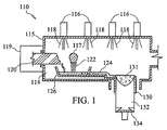
[0036] 本発明は、一部分、金属及び金属合金を溶融させ、且つ(又は)金属鋳造品又は粉体の製造時に使用される材料を溶融状態に維持する電子ビーム炉の改良された設計に関するものである。従来の熱イオン電子ビーム銃溶融炉は、図1に概略図で示されている。炉110は、室の壁115により取り囲まれた真空室114を含む。多数の熱イオン電子ビーム銃116は、室114の外側にて、且つ室114と隣接して配置され、また、別個の線形電子ビーム118を室114内に向ける。金属バー1120及び合金用粉体122の形態をした供給材料が従来のバー供給装置119及び従来の粒子又は粒体供給装置117によりそれぞれ室114内に導入される。電子ビーム銃116の1つの線形電子ビーム118は、バー112の一端に衝突し、且つその一端を溶融させ、その形成される溶融合金124は、室114内の水冷式銅精製炉床126(「冷間炉床」)内に落下する。熱イオン電子ビーム銃116は、従来型式の設計であり、適当なフィラメント材料を加熱することによって電子を発生させる。銃116は、その発生された電子を1点に収束させ、また、電子は、緊密に収束し、実質的に線形ビームの形態にて銃116から投射される。このため、銃116から投射された電子は、基本的に点源として標的に衝突する。この電子の点源による標的の加熱は、カソード光線テレビ受像管の蛍光スクリーンを渡った電子をラスター走査するのと類似した方法にて線形電子ビーム118を標的の少なくとも一部分をラスター走査することにより、促進される。熱イオン電子ビーム銃116の実質的に線形のビーム118をバー120の端部領域を渡ってラスター走査することは、例えば、バー120ーを溶融させることになる。
[0036] The present invention relates to an improved design of an electron beam furnace that partially melts metals and metal alloys and / or maintains the materials used in the manufacture of metal castings or powders in a molten state. It is. A conventional thermionic electron beam gun melting furnace is shown schematically in FIG. The
[0037] 図1を更に参照すると、炉床126内に沈着した溶融合金124は、実質的に線形の電子ビーム118の特定のものを所定の、且つ計画したパターンにて溶融合金124の表面を渡ってラスター走査することにより、溶融状態に維持される。供給装置117により溶融合金124内に導入された粉体又は粒体合金材料は、溶融材料中に組み込まれる。溶融合金124は、炉床126を渡って前進し、且つ、重力によって炉床から銅の引抜き鋳型130内に落下する。引抜き鋳型130は、成長するインゴット132の長さを受容し得るよう並進可能な基部134を含んでいる。溶融合金124は、最初、引抜き鋳型130内に溶融プール131として貯まり、漸進的に、凝固してインゴット132になる。2つ以上の実質的に線形の電子ビーム118をプールの表面を渡ってラスター走査することにより電子が溶融プール131に衝突することは、プール131の領域、特にプールの端縁を溶融状態に維持する点にて有益である。
[0037] With further reference to FIG. 1, the
[0038] 従来の熱イオン電子ビーム銃溶融炉のような、炉室内にて材料を加熱するため2つ以上の実質的に線形の電子ビームを利用する炉において、揮発性成分、すなわち、炉の溶融温度にて相対的に高い蒸気圧力を有する元素は、溶融プールから沸騰し、且つ炉室の相対的に低温の室に凝縮する傾向となる(一般に、電子ビームの溶融により実現される温度にて相対的に高い蒸気圧力を有する一般的な合金成分は、例えば、アルミニウム及びクロムを含む)。実質的に線形の電子ビーム溶融技術は、特に、気化を生じ易く、このことは、少なくとも2つの理由のため、精製又は純化と異なり、合金化するとき、従来の電子ビーム炉の著しく不利益な点である。第一に、合金の全体的な又は局所的な化学的組成は、高揮発性成分が溶融プールから不可避的に失われるため、溶融中、制御が困難となることである。第二に、気化した元素の凝縮物が時間と共に、炉壁に蓄積し勝ちとなり、また、溶融体中に落下し、これにより、溶融を介入物にて汚染し、且つ溶融体の化学的性質に局所的な変化を生じさせることである。 [0038] In a furnace that utilizes two or more substantially linear electron beams to heat material in a furnace chamber, such as a conventional thermionic electron beam gun melting furnace, the volatile components, ie, Elements having a relatively high vapor pressure at the melting temperature tend to boil from the molten pool and condense in a relatively cool chamber of the furnace chamber (typically at a temperature realized by melting of the electron beam). Common alloy components having relatively high vapor pressures include, for example, aluminum and chromium). Substantially linear electron beam melting techniques are particularly prone to vaporization, which differs from refining or purification for at least two reasons, which is a significant disadvantage of conventional electron beam furnaces when alloying. Is a point. First, the overall or local chemical composition of the alloy is difficult to control during melting because highly volatile components are inevitably lost from the molten pool. Second, the vaporized elemental condensate tends to accumulate on the furnace wall over time and also falls into the melt, thereby contaminating the melt with the intervention and the chemical nature of the melt. To cause local changes.
[0039] 何らかの特定の理論に拘束されることを意図せずに、本発明者らは、従来の電子ビーム溶融炉の上記の不利益な点は、電子ビーム炉にて加工された材料に対する従来の実質的に線形の電子ビームの作用に起因するものであると考える。図1の説明に関して上記に言及したように、従来の電子ビーム冷間炉床溶融技術は、実質的に線形の電子ビームを利用して、炉内に導入された原材料を溶融させ、且つ溶融材料が冷間炉床に沿って、且つその上を流れて鋳造鋳型に入るとき、その溶融材料の温度を維持する。かかる炉は、典型的に、多数の電子ビーム源を含んでおり、そのビーム源の各々は、基本的に点源である実質的に線形の電子ビームを作り出す。強力な電子濃度のこれらの「点」は、加熱すべき領域上を迅速にラスター走査し、材料を溶融させ、且つその溶融した材料が十分に流れるのを許容する平均温度がその標的領域の全体を通じて実現されるようにしなければならない。しかし、線形の電子ビームの点源の性質のため、電子ビームが合金に衝突する点は極端な高温度まで加熱される。この局所的に強力な加熱現象は、電子ビームが炉内の固体の又は溶融合金に衝突する特定の点から放出された可視白光線として観察することができる。これらの点にて生ずる強力な過熱効果は、炉室内にて維持された高い真空圧と共に、合金内の相対的に揮発性の元素を容易に気化させ、揮発性成分は過剰に気化し、且つこれと同時に、室の壁に凝縮する結果となる。上述したように、かかる凝縮は、凝縮した材料が溶融合金内に落下するとき、その浴を汚染させ、また、その結果、例えば、鋳造したインゴットにて顕著な組成の不均一性を生じさせる危険性がある。 [0039] Without intending to be bound by any particular theory, the inventors have found that the above disadvantages of conventional electron beam melting furnaces are that of conventional materials processed in electron beam furnaces. This is considered to be caused by the action of the substantially linear electron beam. As noted above with respect to the description of FIG. 1, the conventional electron beam cold hearth melting technique utilizes a substantially linear electron beam to melt the raw material introduced into the furnace and the molten material. Maintains the temperature of the molten material as it flows along and over the cold hearth and enters the casting mold. Such furnaces typically include a number of electron beam sources, each of which produces a substantially linear electron beam that is essentially a point source. These “points” of strong electron concentration are quickly raster scanned over the area to be heated, the average temperature allowing the material to melt, and allowing the molten material to flow sufficiently. Must be realized through. However, due to the nature of the linear electron beam point source, the point where the electron beam strikes the alloy is heated to an extremely high temperature. This locally intense heating phenomenon can be observed as visible white light emitted from a specific point where the electron beam impinges on a solid or molten alloy in the furnace. The strong overheating effect that occurs at these points, along with the high vacuum pressure maintained in the furnace chamber, easily vaporizes relatively volatile elements in the alloy, volatile components are excessively vaporized, and At the same time, this results in condensation on the walls of the chamber. As noted above, such condensation can contaminate the bath when the condensed material falls into the molten alloy and, as a result, can create significant compositional non-uniformities in, for example, cast ingots. There is sex.
[0040] 本明細書にて説明した改良された電子ビーム溶融炉の設計は、例えば、かかる炉内の電子源の少なくとも一部として、ワイヤー放電イオンプラズマ電子エミッタのような、2つ以上のイオンプラズマ電子エミッタを利用する。ワイヤー放電イオンプラズマ電子エミッタは、本明細書にて、一例としてのイオンプラズマエミッタとして開示されているが、以下に更に詳細に説明するように、本発明と共に、その他の適当なイオンプラズマ電子エミッタ(例えば、非ワイヤー放電イオンプラズマ電子エミッタ)を使用することが可能であることを理解すべきである。本明細書にて使用するように、「イオンプラズマ電子エミッタ」及び「ワイヤー放電イオンプラズマ電子エミッタ」という語は、正に帯電したイオンをカソードに衝突させ、これにより二次的な電子フィールドをカソードから解放することにより、相対的に幅の広い非線形の電子フィールドを作り出す装置を意味する。イオンプラズマ電子エミッタにより作り出された電子ビームは、線形ビームではなく、三次元的な電子フィールドすなわち電子の「フラッド(flood)」であり、これらの電子は、標的に衝突したとき、実質的に線形の電子ビームを標的に衝突させることにより包含される小さい点と比べて極めて大きい二次元的領域を包含する。従って、イオンプラズマ電子エミッタにより作り出された電子フィールドは、電子ビーム溶融炉にて使用される従来の電子銃により作り出された遥に小さい接触点に比して本明細書にて「広い面積の」電子フィールドと称する。ワイヤー放電イオンプラズマ電子エミッタは、当該分野にて既知であり(関連しない用途にて使用するため)、且つ例えば、「ワイヤーイオンプラズマ(WIP)電子」銃又はエミッタ、「WIP電子」銃又はエミッタ、また、多少、混乱気味に、「線形電子ビームエミッタ(装置の特定の実施の形態にてプラズマを作り出すワイヤー電極の線形の性質のものを指す)のように、色々な名称にて呼ばれている。 [0040] The improved electron beam melting furnace design described herein includes two or more ions, such as, for example, a wire discharge ion plasma electron emitter, as at least a portion of an electron source in such a furnace. A plasma electron emitter is used. The wire discharge ion plasma electron emitter is disclosed herein as an example ion plasma emitter, but as described in more detail below, in conjunction with the present invention, other suitable ion plasma electron emitters ( It should be understood that, for example, non-wire discharge ion plasma electron emitters can be used. As used herein, the terms “ion plasma electron emitter” and “wire discharge ion plasma electron emitter” are used to cause positively charged ions to collide with the cathode, thereby causing a secondary electron field to be applied to the cathode. Means a device that creates a relatively wide non-linear electronic field. The electron beam produced by the ion plasma electron emitter is not a linear beam, but a three-dimensional electron field or “flood” of electrons, which are substantially linear when they strike the target. It includes a two-dimensional region that is very large compared to the small points that are involved by impinging the target electron beam on the target. Thus, the electron field created by the ion plasma electron emitter is referred to herein as a “wide area” compared to the much smaller contact point created by a conventional electron gun used in an electron beam melting furnace. This is called an electronic field. Wire discharge ion plasma electron emitters are known in the art (for use in unrelated applications) and include, for example, “wire ion plasma (WIP) electron” guns or emitters, “WIP electron” guns or emitters, Also, somewhat confusingly, it is called by various names, such as “linear electron beam emitter (which refers to the linear nature of the wire electrode that produces the plasma in a particular embodiment of the device). .
[0041] ワイヤー放電イオンプラズマ電子エミッタは、多様な設計にて利用可能であるが、かかるエミッタの全ては、特定の基本的な設計上の特徴を共通にする。かかるエミッタの各々は、カチオンを含むプラズマを作り出す細長いワイヤーアノードの形態をした陽イオン源と、ワイヤーにより発生された陽イオンを捕捉するため隔て、且つ位置決めされたカソードとを含むプラズマ又はイオン化領域を含む。大きい負電圧がカソードに印加されて、ワイヤー陽イオン源により発生されたプラズマ内の陽イオンの一部分は、カソード表面に向けて加速され、且つそのカソード表面と衝突し、カソードから二次的電子が放出される(「一次的」電子は陽イオンと共に、プラズマ内に存在する)。カソード面から作り出された二次的電子は、カソードにぶつかる、陽イオンプラズマの三次元的形状を通常有する非線形の電子フィールドを形成する。次に、その二次的電子は、カソードの付近からアノードに向けて加速され、エミッタ内の低圧の気体を通過する過程にてほとんど衝突を経験しない。ワイヤー放電イオンプラズマ電子エミッタの色々な構成要素を適正に設計し、且つ配置することにより、活発な二次的電子の広いフィールドをカソードにて形成し、且つエミッタから標的に向けて加速することができる。図2は、ワイヤー放電プラズマイオン電子エミッタの構成要素の概略図であり、電流が細いワイヤーアノード12に印加されて、プラズマ14を発生させる。プラズマ14内の陽イオン16は、負に帯電したカソード18に向けて加速され、且つそのカソードと衝突して、広い面積の二次的電子クラウド20を解放し、この電子クラウドは、電極間の且つ標的に向けた電界の動作によりアノード12の方向に加速される。
[0041] Although wire discharge ion plasma electron emitters are available in a variety of designs, all such emitters share certain basic design features. Each such emitter has a plasma or ionization region that includes a cation source in the form of an elongated wire anode that creates a plasma containing cations and a cathode positioned spaced and positioned to capture the cations generated by the wire. Including. When a large negative voltage is applied to the cathode, a portion of the cations in the plasma generated by the wire cation source is accelerated towards and collides with the cathode surface, and secondary electrons are emitted from the cathode. Emitted ("primary" electrons are present in the plasma along with positive ions). The secondary electrons created from the cathode surface form a non-linear electron field that typically has the three-dimensional shape of a cation plasma that strikes the cathode. The secondary electrons are then accelerated from near the cathode toward the anode and experience little collision in the process of passing through the low pressure gas in the emitter. By properly designing and arranging the various components of the wire discharge ion plasma electron emitter, a wide field of active secondary electrons can be formed at the cathode and accelerated from the emitter toward the target. it can. FIG. 2 is a schematic diagram of the components of a wire discharge plasma ion electron emitter, in which a current is applied to a
[0042] 本発明の1つの非限定的な実施の形態に従い、電子ビーム溶融炉の形態にて導電性の金属材料を溶融させる装置は、真空室(溶融室)と、該真空室内に配置され、且つ溶融材料を保持し得るようにされた炉床とを含む。少なくとも1つのワイヤー放電イオンプラズマエミッタが真空室内に又は真空室に隣接して配置されており、また、エミッタにより発生された非線形の広い面積の電子フィールドを室内に向けるよう位置き決めされている。ワイヤー放電イオンプラズマ電子エミッタは、導電性の金属材料をその溶融温度まで加熱するのに十分なエネルギを有する非線形の電子フィールドを作り出す。鋳型又はその他の鋳造又は噴霧装置が室と連通状態に配置され、また、炉床から材料を受け取るように位置決めされている。例えば、チタン、チタン合金、タングステン、ニオブ、タンタル、白金、パラジウム、ジルコニウム、イリジウム、ニッケル、ニッケル系合金、鉄、鉄系合金、コバルト、及びコバルト系合金のような、従来の電子ビーム溶融炉を使用して溶融させることのできる任意の材料を炉床を使用して溶融させることができる。 [0042] According to one non-limiting embodiment of the present invention, an apparatus for melting a conductive metal material in the form of an electron beam melting furnace is disposed in a vacuum chamber (melting chamber) and the vacuum chamber. And a hearth adapted to hold molten material. At least one wire discharge ion plasma emitter is disposed in or adjacent to the vacuum chamber and is positioned to direct a non-linear, large area electron field generated by the emitter into the chamber. A wire discharge ion plasma electron emitter creates a non-linear electron field having sufficient energy to heat a conductive metal material to its melting temperature. A mold or other casting or spraying device is placed in communication with the chamber and is positioned to receive material from the hearth. For example, conventional electron beam melting furnaces such as titanium, titanium alloys, tungsten, niobium, tantalum, platinum, palladium, zirconium, iridium, nickel, nickel alloys, iron, iron alloys, cobalt, and cobalt alloys. Any material that can be used and melted can be melted using the hearth.
[0043] 本発明に従った電子ビーム溶融炉の実施の形態は、導電性材料又はその他の合金添加物を真空室内に導入し得るようにされた2つ以上の材料供給装置を含むことができる。好ましくは、供給装置は、材料を炉床の少なくとも1つの領域の上方の位置にて真空室内に導入し、固体又は溶融形態の材料が重力にて下方の炉床内に落下するのを許容するようにする。供給装置の型式は、例えば、バー供給装置及びワイヤー供給装置とし、選ばれる供給装置の型式は、炉の特定の設計上の条件に依存するものとなるであろう。本発明による炉の特定の実施の形態において、材料の供給装置、及び炉の2つ以上のワイヤー放電イオンプラズマ電子エミッタの少なくとも1つは、ワイヤー放電イオンプラズマ電子エミッタにより放出された電子フィールドが少なくとも部分的に、供給装置により室内部に導入された材料に衝突するよう配置されている。供給装置により真空室内に導入された材料が導電性である場合、電子フィールドは、十分な強度があるならば、その材料を加熱し、且つ溶融させるであろう。 [0043] Embodiments of an electron beam melting furnace in accordance with the present invention may include two or more material supply devices adapted to introduce conductive materials or other alloy additives into the vacuum chamber. . Preferably, the feeder device introduces material into the vacuum chamber at a location above at least one region of the hearth and allows the solid or molten form of material to fall into the lower hearth under gravity. Like that. Feeder types may be, for example, bar feeders and wire feeders, and the type of feeder chosen will depend on the specific design requirements of the furnace. In a particular embodiment of the furnace according to the invention, at least one of the material supply device and the two or more wire discharge ion plasma electron emitters of the furnace has at least an electron field emitted by the wire discharge ion plasma electron emitter. In part, it is arranged to collide with the material introduced into the room by the supply device. If the material introduced into the vacuum chamber by the feeder is conductive, the electronic field will heat and melt the material if it is strong enough.
[0044] 本発明に従った溶融炉の実施の形態に組み込んだ炉床は、当該分野にて既知の色々な型式の炉床から選ぶことができる。例えば、炉は、冷間炉床、又はより特定的には、例えば、水冷式銅冷間炉床を真空室内に組み込むことにより、電子ビーム冷間炉床溶融炉の性質のものとすることができる。当業者に既知であるように、冷間炉床は、炉床内の溶融材料を炉床の表面に凍結させ、保護層を形成するための冷却手段を含んでいる。別の例として、炉床は、炉内にて溶融される合金にてめっきし又はその合金にて製作した炉床である、「自原的(autogenous)」炉床とすることができ、その場合、炉床の底面は、焼付きを防止するよう水冷式とすることができる。 [0044] The hearth incorporated into the embodiment of the melting furnace according to the present invention can be selected from various types of hearths known in the art. For example, the furnace may be of the nature of an electron beam cold hearth melting furnace by incorporating a cold hearth, or more specifically, a water-cooled copper cold hearth, for example, in a vacuum chamber. it can. As known to those skilled in the art, the cold hearth includes cooling means for freezing the molten material in the hearth to the surface of the hearth and forming a protective layer. As another example, the hearth can be an “autogenous” hearth, which is a hearth plated with or made from an alloy that is melted in the furnace, In that case, the bottom of the hearth can be water-cooled to prevent seizure.
[0045] 真空室内に含めた特定の炉床は、溶融材料の保持領域を含むことができ、その場合、溶融材料は、特定の休止時間の間、その保持領域に止まり、その後、真空室と流体的に接続された鋳造又は噴霧装置に流れる。本発明に従った炉の特定の実施の形態において、炉床、及び少なくとも1つの炉の2つ以上ワイヤー放電イオンプラズマ電子エミッタは、ワイヤー放電イオンプラズマ電子エミッタにより放出された電子フィールドが溶融材料の保持領域に少なくとも部分的に衝突するように配置されている。このようにして、電子フィールドは、溶融材料の保持領域内の材料を溶融状態に維持すべく印加することができ、また、電子フィールドの加熱作用が溶融材料をガス抜きし、且つ精製する働きをするようにすることができる。 [0045] A particular hearth included in the vacuum chamber may include a holding area for the molten material, in which case the molten material will remain in that holding area for a specific downtime, after which the vacuum chamber and Flow to a fluidly connected casting or spraying device. In a particular embodiment of the furnace according to the invention, the hearth and at least one furnace of two or more wire discharge ion plasma electron emitters of the furnace are such that the electron field emitted by the wire discharge ion plasma electron emitter is of molten material. It is arranged to at least partially collide with the holding area. In this way, the electron field can be applied to maintain the material in the molten material holding region in a molten state, and the heating action of the electron field serves to degas and purify the molten material. To be able to.
[0046] 本発明に従った炉の特定の非限定的な実施の形態は、溶融材料を鋳造する鋳型を含む。該鋳型は、例えば、静止鋳型、引抜き鋳型又は連続鋳造鋳型のような、当該分野にて既知の任意の適当な鋳型でよい。これと代替的に、炉は、例えば、溶融材料から粉体材料を製造する噴霧装置を含み、又は該噴霧装置と関係したものとしてもよい。 [0046] Certain non-limiting embodiments of furnaces according to the present invention include a mold for casting molten material. The mold may be any suitable mold known in the art such as, for example, a stationary mold, a drawn mold or a continuous casting mold. Alternatively, the furnace may include or be associated with, for example, a spraying device that produces powdered material from a molten material.
[0047] 本発明に従った電子ビーム溶融炉の1つの特定の非限定的な例は、真空室と、該真空室内に配置された炉床とを含み、該炉床は、溶融材料の保持領域を含む。該炉は、真空室内に又は真空室に隣接して配置された2つ以上のワイヤー放電イオンプラズマ電子エミッタを更に含む。炉床及び少なくとも1つのワイヤー放電イオンプラズマ電子エミッタは、エミッタにより作り出された電子フィールドが溶融材料の保持領域に少なくとも部分的に衝突するよう配置されている。引抜き鋳型は、真空室と連通しており、且つ、炉床から溶融材料を受け取るよう位置決めされている。少なくとも1つの供給装置が炉の内部に含まれており、且つ炉床の少なくとも1つの領域の上方にて材料を真空室内に導入し得るようにされている。 [0047] One specific, non-limiting example of an electron beam melting furnace according to the present invention includes a vacuum chamber and a hearth disposed in the vacuum chamber, the hearth holding molten material. Includes area. The furnace further includes two or more wire discharge ion plasma electron emitters disposed in or adjacent to the vacuum chamber. The hearth and at least one wire discharge ion plasma electron emitter are arranged such that the electron field created by the emitter at least partially impinges on the holding area of the molten material. The drawing mold is in communication with the vacuum chamber and is positioned to receive molten material from the hearth. At least one supply device is included within the furnace and is adapted to introduce material into the vacuum chamber above at least one region of the hearth.
[0048] 本発明に従った装置と関係して任意の適当なワイヤー放電イオンプラズマ電子エミッタを使用することができる。ワイヤー放電イオンプラズマ電子エミッタの適当な実施の形態は、例えば、その開示内容の全体を参考として引用し、本明細書に含めた米国特許第4,025,818号明細書、米国特許第4,642,522号明細書、米国特許第4,694,222号明細書、米国特許第4,755,722号明細書及び米国特許第4,786,844号明細書に開示されている。適当なエミッタは、炉の真空室内に向けることができ、また、炉室内に配置された導電性の供給材料を所望の温度まで加熱する非線形の広い面積の電子フィールドを作り出すことができるものを含む。 [0048] Any suitable wire discharge ion plasma electron emitter can be used in connection with the apparatus according to the present invention. Suitable embodiments of wire discharge ion plasma electron emitters are described, for example, in U.S. Pat. No. 4,025,818, U.S. Pat. No. 642,522, U.S. Pat. No. 4,694,222, U.S. Pat. No. 4,755,722 and U.S. Pat. No. 4,786,844. Suitable emitters include those that can be directed into the vacuum chamber of the furnace and can create a non-linear, large area electron field that heats the conductive feed disposed in the furnace chamber to a desired temperature. .
[0049] ワイヤー放電イオンプラズマ電子エミッタの1つの実施の形態において、エミッタは、プラズマ領域と、カソード領域とを含んでいる。該プラズマ領域は、陽イオンを含むプラズマを作り出し得るようにされた少なくとも1つの細長いワイヤーアノードを含む。カソード領域は、カソードを負に帯電させ得るようにした高電圧電源と電気的に接続されたカソードを含む。ワイヤー放電イオンプラズマ電子エミッタにおいて、プラズマを作り出すべく使用される電極は、プラズマ領域の長さに沿って位置決めされた1本のワイヤー又は多数のワイヤーとすることができる。陽イオンがぶつかるカソードの少なくとも一部分は、電子を発生させるのに適した材料にて出来たものとする。エミッタのカソード領域内に配置されたカソードの特定の非限定的な実施の形態は、また、例えば、高い溶融温度及び低い作用機能を有し、電子の発生を促進するモリブデン挿入体のような、挿入体を含むこともできる。カソード及びアノードは、ワイヤーアノードにより発生されたプラズマ中の陽イオンが電極間の電界の影響の下、カソードに向けて加速され、且つカソードに衝突し、二次的電子の広い面積のフィールドをカソードから解放するように互いに位置決めされている。 [0049] In one embodiment of a wire discharge ion plasma electron emitter, the emitter includes a plasma region and a cathode region. The plasma region includes at least one elongated wire anode adapted to create a plasma containing positive ions. The cathode region includes a cathode that is electrically connected to a high voltage power supply that is capable of negatively charging the cathode. In a wire discharge ion plasma electron emitter, the electrode used to create the plasma can be a single wire or multiple wires positioned along the length of the plasma region. It is assumed that at least a part of the cathode where the cation collides is made of a material suitable for generating electrons. Certain non-limiting embodiments of the cathode disposed within the cathode region of the emitter can also have, for example, a molybdenum insert that has a high melting temperature and a low working function and promotes the generation of electrons, such as Inserts can also be included. In the cathode and anode, positive ions in the plasma generated by the wire anode are accelerated toward the cathode under the influence of the electric field between the electrodes, and collide with the cathode, so that a large area field of secondary electrons is cathoded. Are positioned relative to each other so as to release.
[0050] ワイヤー放電イオンプラズマ電子エミッタの特定の非限定的な実施の形態は、薄い電子透過性チタン又はアルミニウムフォイルのような、少なくとも1つの適当な電子透過性窓部を含み、この窓部は、炉の真空室の壁に開口する。電子透過性窓部を形成するための代替的な材料は、例えば、BN、ダイヤモンド、及び原子番号の小さい元素から成る特定のその他の材料を含む。本明細書にて説明したように、ワイヤー放電イオンプラズマ電子エミッタのその他の実施の形態は、電子透過性窓を含まず、この場合、エミッタのプラズマ領域は、溶融材料を保持する真空室と流体的に連通している。その何れの場合でも、得られた広い面積の電子フィールドは、炉室に入り、且つ室内の材料に衝突することができる。電子透過性窓が電子エミッタの内部を真空室から分離しない場合(本明細書にて更に説明するように)、電子フィールドは、電子エミッタから真空室内に投射されるとき、窓を通って流れる。ワイヤー放電イオンプラズマ電子エミッタの特定の非限定的な実施の形態において、カソードと電気的に連結された高電圧電源は、カソードを20,000ボルト以上の負電圧に給電する。この負電圧は、プラズマ内の陽イオンをカソードに向け、その後、二次的電子フィールドをカソードから且つアノードに向けて反発させる。 [0050] Certain non-limiting embodiments of wire discharge ion plasma electron emitters include at least one suitable electron permeable window, such as a thin electron permeable titanium or aluminum foil, Open into the vacuum chamber wall of the furnace. Alternative materials for forming the electron transmissive window include, for example, BN, diamond, and certain other materials consisting of elements with a low atomic number. As described herein, other embodiments of wire discharge ion plasma electron emitters do not include an electron transmissive window, in which case the plasma region of the emitter includes a vacuum chamber and a fluid holding molten material. Are communicating. In either case, the resulting large area electron field can enter the furnace chamber and collide with the material in the chamber. If the electron transmissive window does not separate the interior of the electron emitter from the vacuum chamber (as will be further described herein), the electron field flows through the window when projected from the electron emitter into the vacuum chamber. In a specific, non-limiting embodiment of a wire discharge ion plasma electron emitter, a high voltage power source electrically connected to the cathode supplies the cathode to a negative voltage of 20,000 volts or more. This negative voltage directs the cations in the plasma toward the cathode and then repels the secondary electron field from the cathode toward the anode.
[0051] ワイヤー放電イオンプラズマ電子エミッタ内の圧力が炉室内の圧力と実質的に相違する場合、フォイル窓部は、圧力の異なる2つの隣接する領域を隔離する働きをする。熱イオン電子ビーム銃のような、気体を保持しない電子エミッタに比して、ワイヤー放電イオンプラズマ電子エミッタの1つの有利な点は、ワイヤー放電イオンプラズマ電子エミッタは、プラズマ源として作用するようプラズマ領域内に気体を含まなければならない点である。ワイヤー放電イオンプラズマ電子エミッタは、極めて低い気体圧力にて作動可能であるが、かかる装置は、また、比較的高い気体圧力にても作動可能である。これに反して、従来の電子ビーム溶融炉は、一般に、超低圧の真空状態にて作動し、この場合、ワイヤー放電イオンプラズマ電子エミッタ内の気体雰囲気を炉室内の近真空環境から分離するため、電子透過性窓部が必要であろう。しかし、炉室内の気体圧力を従来の線形(熱イオンエミッタ)電子ビーム溶融炉内の超低圧のレベル以上に増大させることにより、炉室内での揮発性成分の気化を少なくすることができると考えられる。これらの従来の圧力レベルは、通常、10−3から7.5μ(10−3から1Pa)内にあり、15μ(2Pa)を超えることはない。炉室内の圧力が従来のレベル、すなわち、40μ(5.3Pa)を超え、又はより好ましくは、300μ(40Pa)を超えるまで上昇させると、炉内の溶融材料の表面の圧力が上昇し、これにより、望ましくない気化を生じさせる推進力を減少させる。例えば、「真空金属加工における気化の理論的及び実験的アプローチ(Theoretical and Experimental Approach of the Volatilization in Vacuum Metallurgy)」にてH.デュバル(Duval)らにより報告されたデータは、クロムの蒸気の輸送量は4.27Pa(35ミリトル)アルゴンに比して、66.7Pa(500ミリトル)アルゴンにて実質的に減少することを示唆している。ワイヤー放電イオンプラズマ電子エミッタは、既に、部分気体圧力の環境(典型的に、ヘリウム)が作用可能であることを要求しているため、本発明者らは、ワイヤー放電イオンプラズマ電子エミッタ及び炉室の双方を実質的の同一の圧力にて作動させることが可能であり、その圧力は、電子エミッタが作動するのを許容するのに十分高圧であり、且つ従来の電子ビーム炉内の圧力よりも高く、これにより炉室内での望ましくない気化を減少させることが可能であると考える。かかる場合、電子透過性窓部を省略し、エミッタ及び炉室内の気体環境は実質的に同一であるようにすることができる。これと代替的に、ワイヤー放電イオンプラズマ電子エミッタの別の実施の形態において、該エミッタにより発生された電子は、電子透過性の気体不透過性窓部を通過し、該エミッタ内のイオン化可能な気体の圧力は、電子エミッタが作動するのに適しており、炉室は、電子ビーム炉内の圧力よりも高い圧力にて作動し、且つ望ましくない気化を最小にし又は減少させるのに適している。望ましくない元素の気化の減少は、強力な加熱点を作り出さない2つ以上のワイヤー放電イオンプラズマ電子エミッタを利用することと、電子ビーム炉内にて従来よりも高い炉室の圧力とすることとの双方により、最適化することができることが理解されよう。 [0051] If the pressure in the wire discharge ion plasma electron emitter is substantially different from the pressure in the furnace chamber, the foil window serves to isolate two adjacent regions of different pressure. One advantage of a wire discharge ion plasma electron emitter over an electron emitter that does not hold a gas, such as a thermionic electron beam gun, is that the wire discharge ion plasma electron emitter acts as a plasma source so that it acts as a plasma source. It is a point that must contain gas. While wire discharge ion plasma electron emitters can operate at very low gas pressures, such devices can also operate at relatively high gas pressures. On the other hand, conventional electron beam melting furnaces generally operate in ultra-low pressure vacuum conditions, in which case the gas atmosphere in the wire discharge ion plasma electron emitter is separated from the near vacuum environment in the furnace chamber, An electron transmissive window would be necessary. However, by increasing the gas pressure in the furnace chamber beyond the ultra-low pressure level in the conventional linear (thermal ion emitter) electron beam melting furnace, the vaporization of volatile components in the furnace chamber can be reduced. It is done. These conventional pressure levels are usually in the range of 10 −3 to 7.5 μ (10 −3 to 1 Pa) and do not exceed 15 μ (2 Pa). Increasing the pressure in the furnace chamber to a conventional level, that is, exceeding 40 μ (5.3 Pa), or more preferably exceeding 300 μ (40 Pa), increases the pressure on the surface of the molten material in the furnace. Reduces the driving force that causes undesirable vaporization. See, for example, “Theoretical and Experimental Approach to The Volatilization in Vacuum Metallurgy” in H.V. Data reported by Duval et al. Suggests that chromium vapor transport is substantially reduced at 66.7 Pa (500 mTorr) argon compared to 35 mTorr argon. doing. Since wire discharge ion plasma electron emitters already require that a partial gas pressure environment (typically helium) be able to operate, we have wire discharge ion plasma electron emitters and furnace chambers. Can be operated at substantially the same pressure, which is sufficiently high to allow the electron emitter to operate and higher than that in a conventional electron beam furnace. It is believed that this can reduce undesirable vaporization in the furnace chamber. In such a case, the electron permeable window may be omitted, and the gas environment in the emitter and the furnace chamber may be substantially the same. Alternatively, in another embodiment of a wire discharge ion plasma electron emitter, electrons generated by the emitter pass through an electron permeable gas impermeable window and can be ionized within the emitter. The pressure of the gas is suitable for operating the electron emitter, the furnace chamber is operated at a pressure higher than that in the electron beam furnace, and is suitable for minimizing or reducing undesirable vaporization. . Undesirable element vaporization is reduced by utilizing two or more wire discharge ion plasma electron emitters that do not create a strong heating point, and by using a higher chamber pressure in the electron beam furnace. It will be appreciated that both can be optimized.
[0052] 本発明に従った炉に関連して有用な電子ビーム溶融炉の可能な実施の形態及びワイヤー放電イオンプラズマ電子エミッタの可能な実施の形態の更なる説明について、以下に記載する。 [0052] Further descriptions of possible embodiments of electron beam melting furnaces useful in connection with furnaces according to the present invention and possible embodiments of wire discharge ion plasma electron emitters are described below.
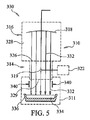
[0053] 図3には、本発明に従った改良されたビーム溶融炉の1つの可能な非限定的な実施の形態が概略図にて示されている。炉210は、室の壁215により少なくとも部分的に規定された真空室214を含んでいる。ワイヤー放電イオンプラズマ電子エミッタ216は、室214の外側にて、且つ室124に隣接して位置決めされている。ワイヤー放電イオンプラズマ電子エミッタ216は、広い面積の電子フィールド218を室214の内部に投射する。図1に示した従来の炉110に類似して、合金バー220は、バー供給装置219により室214内に導入される。溶融合金226は、少なくとも1つのワイヤー放電イオンプラズマ電子エミッタ216の広い面積の電子フィールド218をバー220に衝突させることにより製造される。バー220から溶融させた溶融合金226は、水冷式銅炉床224内に落下し、且つ特定の休止時間、炉床224内に止まり、その炉床にて、合金は、エミッタ216により作り出された広い面積の2つ以上の電子フィールド218により加熱、ガス抜きされ、且つ精製される。溶融合金226は、最終的に、炉床224から銅鋳型230内に落下し、溶融したプール231を形成する。溶融したプール231は、最終的に、且つ漸進的に、鋳型230内にて凝固し、インゴット232を形成する。広い面積の電子フィールド218の少なくとも1つは、形成するインゴット232の凝固率を制御するのと同様の仕方にてプール231内の溶融合金を加熱することが好ましい。
[0053] FIG. 3 schematically illustrates one possible non-limiting embodiment of an improved beam melting furnace according to the present invention. The
[0054] 上述したように、炉210のワイヤー放電イオンプラズマ電子エミッタ216は、従来の電子ビーム炉内にて使用される電子ビーム銃により作り出された実質的に線形ビームの点の包含範囲に比して、広い面積を包含する活発な電子フィールド又は「フラッド」を発生させる設計とされている。電子フィールドエミッタ216は、電子を広い面積にてまき拡げ、且つ材料に衝突し溶融させ、且つ(又は)炉210内にて溶融状態に維持される。エミッタが作り出す電子フィールドは、炉の室内にて広い面積を包含するから、ワイヤー放電イオンプラズマ電子エミッタは、従来の電子ビーム炉に比して、電子ビーム溶融炉内にて一層均一な温度を維持し、また、高度に収束した電子の点をラスター走査することを不要にする。しかし、本発明に従った電子ビーム炉の特定の実施の形態は、所望に応じて、2つ以上のワイヤー放電イオンプラズマ電子エミッタにより発生された電子フィールドをステアするため、電界を発生させる構成要素又はその他の適当な構成要素を含むことができる。例えば、炉210内にて、ワイヤー放電イオンプラズマ電子エミッタ216により作り出された広いフィールドを側方向にラスター走査して、炉床224の端縁に対し追加的な熱を提供することが望ましいであろう。比較的広い面積をわたって電子の点源をラスター走査するのではなくて、活発な電子フィールドにてその広い面積をフラッドさせることにより、従来の電子ビーム溶融炉を使用するとき生ずる実質的に線形の電子ビームと関係した局所的に強力な加熱効果(例えば、単位面積当たりの電力)は、実質的に減少する。このことは、比較的極めて高温度の点が形成されないことを理由として、比較的揮発性の合金成分の望ましくなく気化の程度を少なくとも実質的に減少させることになる。このことは、一方、従来の電子ビーム炉の設計に本来的な組成物の制御及び汚染の問題点を部分的に又は全体的に解消することになる。
[0054] As mentioned above, the wire discharge ion
[0055] 上述したように、ワイヤー放電イオンプラズマ電子エミッタの色々な実施の形態は、全体として、陽イオンプラズマを作り出すアノードを有する2つ以上の細長いワイヤーアノードを含み、プラズマは、カソードに衝突して、二次的電子のフィールドを発生させ、この電子フィールドは、加速して加熱すべき標的に衝突するようにすることができる。その他の関連しない用途にて以前から使用されている1つの既知の設計のワイヤー放電イオンプラズマ電子エミッタの概略図が図4に示されている。このエミッタ310は、その内部にて陽イオンプラズマが作り出されるイオン化領域又はプラズマ領域314と、カソード318を包含するカソード領域316とを含んでいる。プラズマ領域314は、イオン化可能な気体が低圧にて充填されており、また、その気体は、プラズマ領域内にてイオン化され、カチオンを保持するプラズマを作り出す。例えば、イオン化領域314は、例えば、約20ミリトルのヘリウムガスにて充填することができる。小径の細長いワイヤーアノード319は、長いプラズマ領域314を通って流れる。正電圧が電源322によりワイヤーアノード319に印加され、このことは、ヘリウムガスをイオン化してヘリウムカチオン及び自由電子(「一次的電子」)から成るプラズマにする工程を開始する。ヘリウムガスのイオン化が開始されると、プラズマは、細いワイヤーアノード319に電圧を印加することにより支えられる。プラズマ内の正に帯電したヘリウムイオンは、高い負の電位に維持された引出し格子326を通じてイオン化室314から引き出され、且つ高い電圧空隙を通ってカソード領域316内に加速され、このカソード領域内にて、プラズマ中のカチオンは、高い負電圧のカソード318にぶつかる。カソード318は、例えば、被覆し又は非被覆の金属又は合金とすることができる。ヘリウムイオンがカソード318に衝突すると、カソード318から二次的電子が解放される。高電圧の空隙328は、引出し格子326を通ってプラズマ領域314内に、次に、電子に対して比較的透過性の材料にて出来た薄い金属フォイル窓部329を通して、ヘリウムカチオンが移動する方向と反対の方向に向けて二次的電子を加速する。上述したように、電子エミッタ及び炉室内の相対的な気体圧力に依存して、フォイル窓部329を省略することが可能であり、この場合、エミッタにより作り出された電子は炉室に直接、入るであろう。
[0055] As described above, various embodiments of a wire discharge ion plasma electron emitter generally include two or more elongated wire anodes having an anode that creates a positive ion plasma, the plasma impinging on the cathode. Thus, a field of secondary electrons can be generated that can be accelerated to impinge on the target to be heated. A schematic diagram of one known design wire discharge ion plasma electron emitter previously used in other unrelated applications is shown in FIG. The
[0056] ワイヤー電極319及びカソード318は、正に帯電したヘリウムイオンのカソード318への移動を一層促進する設計及び配置とすることができる。また、カソード318及び引出し格子326は、格子326を通る二次的電子の透過を最大にし、且つフォイル窓部329(存在するならば)への侵入に適したビーム外形を有する設計及び配置とさすることができる。エミッタ310から出る広い面積の活発な電子フィールドは、フォイル窓部329と対向する位置にて、且つ溶融炉の真空室内に位置決めされた標的に衝突するよう向けることができる。また、窓部329は、エミッタ310からの電子の透過を最大にし得るよう可能な限り薄い寸法とすることができる。エミッタ310内にて僅かな真空環境を維持しつつ、十分な電子の透過を許容する厚さを有するアルミニウム型式又はチタン型式のフォイルを必要であるならば、フォイル窓部329として使用することができる。装置の窓として(存在するならば)使用することのできるその他の適当に丈夫で且つ許容可能な電子透過性材料は当業者に既知であろう。本明細書にて全体的に説明したように、窓部329は、エミッタ310内部の圧力と標的を保持する真空室内との圧力差が大きくないならば、省略することができる。
[0056] The
[0057] 本発明に従って、実質的に線形の電子ビームを作り出す電子ビーム銃の代替品として、例えば、エミッタ310のような、2つ以上のワイヤー放電イオンプラズマ電子エミッタを、電子ビームの溶融炉内の真空室内に活発な電子を供給するため提供することができる。図5に示したように、本発明に従った電子ビーム溶融炉330の1つの非限定的な実施の形態は、真空室311に隣接して位置決めされた2つ以上のワイヤー放電イオンプラズマ電子エミッタ310を含んでいる。広い面積の電子フィールド332は、フィルム窓部329を通ってエミッタ310から出て、且つ炉床336内にて溶融合金334の表面の少なくとも1つの領域にてフラッドして、これにより合金を加熱して、合金を溶融状態に維持する。炉床336内にて合金に衝突する電子は、比較的広い面積にわたってまき拡げられるから、任意の特定の局所的領域内にて溶融材料上に収束されたエネルギは、合金からの元素の気化レベルが問題となる程、十分に大きくはなく、これにより、従来の電子ビーム溶融炉の使用に本来的な合金の汚染及び不均一性という問題点を減少させ又は解消する。上述したように、エミッタ310と真空室311との作用圧力差が大きくない場合、フィルム窓部329を省略することができる。また、上述したように、真空室311は、従来の圧力よりも高い圧力にて作動し、望ましくない元素の気化を更に減少させ又は解消することが好ましく、かかる場合、電子エミッタを炉室から仕切るフィルム窓部の必要性は、この場合にも、設計に本来的な特定の圧力差に依存するものとなるであろう。選択的に、真空室311内の溶融過程を更に良く制御するため、広い面積の電子フィールドを磁気的にステアする構成要素を提供することができる。
[0057] In accordance with the present invention, as an alternative to an electron beam gun that produces a substantially linear electron beam, two or more wire discharge ion plasma electron emitters, such as
[0058] 図5は、単一の電子エミッタを含む、本発明に従ったワイヤー放電イオンプラズマ電子溶融炉の1つの実施の形態の簡略化した図を示すが、当業者には、かかる装置の実際の又は代替的な実施の形態は、多数のワイヤー放電イオンプラズマ電子エミッタを有することができることが明らかであろう。また、2つ以上のワイヤー放電イオンプラズマ電子エミッタをかかる装置に組み込んで、次のことを行うこと、すなわち、(1)例えば、合金バー又はワイヤーの形態にて炉内に導入された原材料を溶融させること、(2)炉の炉床内に滞在する溶融合金を合金の溶融温度以上の温度に維持すること(また、可能であれば、溶融合金のガス抜き及び(又は)精製を行うこと)、(3)増分的に前進する鋳造したインゴットの表面上における溶融プールの所望の領域を溶融状態に維持し、これによりインゴットの凝固率に所望の仕方にて影響を与えることができることが明らかであろう。また、特定の実施の形態において、従来の実質的に線形の電子ビームを作り出す2つ以上の電子ビーム銃と共に、2つ以上のワイヤー放電イオンプラズマ電子エミッタを使用することができる。 [0058] FIG. 5 shows a simplified diagram of one embodiment of a wire discharge ion plasma electron melting furnace according to the present invention comprising a single electron emitter, although those skilled in the art will be familiar with such an apparatus. It will be apparent that actual or alternative embodiments can have multiple wire discharge ion plasma electron emitters. Also, incorporate two or more wire discharge ion plasma electron emitters into such an apparatus to do the following: (1) Melt the raw material introduced into the furnace, for example in the form of an alloy bar or wire (2) Maintain the molten alloy staying in the hearth of the furnace at a temperature equal to or higher than the melting temperature of the alloy (and, if possible, degas and / or purify the molten alloy). (3) It is clear that the desired region of the molten pool on the surface of the incrementally advanced cast ingot can be maintained in a molten state, thereby affecting the solidification rate of the ingot in a desired manner. I will. Also, in certain embodiments, two or more wire discharge ion plasma electron emitters can be used with two or more electron beam guns that produce a conventional substantially linear electron beam.
[0059] 図6及び図7は、本発明に従った電子ビーム溶融炉内の1つの実施の形態にて活発な電子の供給源として使用し得るようにすることのできるワイヤー放電イオンプラズマ電子エミッタ510の1つの実施の形態に関係した更なる詳細を提供する。図6は、ワイヤー放電イオンプラズマ電子エミッタの実施の形態510の一部分断面図とした斜視図である。図7は、エミッタ510の作用を簡略化した仕方にて示す概略図である。エミッタ510は、カソード領域511と、イオン化領域すなわちプラズマ領域514と、電子透過性フォイル窓部515とを含む電気接地した囲い物513を含んでいる。細長いワイヤー電極516が長いイオン化領域514を通って伸びている。フォイル窓部515は、室513と電気的に連結され、これにより、アノードを形成し、このアノードは室513内の電子を加速して、室513から矢印「A」の方向に出るようにする。室513は、1−10ミリトルのような、低圧のヘリウムガスが充填されており、また、該室513には、気体供給源517により気体が供給される。気体供給源517は、弁521を通る導管519により囲い物513と接続されている。導管524により室513と接続されたポンプ523により室513内にて僅かな真空環境が維持されている。
[0059] FIGS. 6 and 7 illustrate a wire discharge ion plasma electron emitter that can be used as a source of active electrons in one embodiment in an electron beam melting furnace according to the present invention. Further details relating to one embodiment of 510 are provided. FIG. 6 is a perspective view with a partial cross-sectional view of a wire discharge ion plasma
[0060] カソード領域511は、カソード518を含む一方、該カソードは、その下面に取り付けた挿入体520を含んでいる。挿入体520は、例えば、モリブデンから成るものとすることができるが、適度に大きい二次的電子の透過率を有する任意の材料から成るものとすることができる。カソード518は、パッシェン(Paschen)破壊を防止するため、囲い物513の壁から適度に均一に隔てられている。カソード518は、絶縁体526を通って抵抗器528内に伸びるケーブル525により高電圧の電源522に連結されている。電源522は、例えば、200−300KVのような高い負電位をカソード518に供給する。カソード518及び挿入体520は、例えば、導管527を通って循環する油又は別の適当な冷却流体等によって適当に冷却することができる。
[0060] The
[0061] イオン化領域514は、電気的に且つ機械的に連結された複数の薄い金属リブ530を含んでいる。リブ530の各々は、ワイヤー電極516がイオン化室514を貫通して伸びるのを許容する中央の切欠き領域を含んでいる。カソード518に面するリブ530の側部は、引出し格子534を形成する。リブ530の全部分又は一分の反対側部は、電子透過性フォイル窓部515に対する支持格子536を提供する。冷却流体をリブ530内にて且つその近くにて循環させ、イオン化領域514から熱を除去するため冷却通路540を設けることができる。例えば、アルミニウム又はチタンフォイルにて出来た電子透過性フォイル窓515は、格子536にて支持され、且つ囲い物513内にて高圧の真空ヘリウム気体環境を維持するのに十分なO−リング又はその他の構造体により囲い物に対して密封されている。エミッタ510の特定の実施の形態において、加圧した窒素等によってフォイル窓部515を冷却すべく気体マニホルドが設けられている。本明細書にて全体として説明したように、エミッタ510の室513の内部と電子フィールドの標的を保持する室との間の圧力差が大きくない場合、窓部515は省略することができる。
[0061] The
[0062] 電気制御装置548は、コネクタ549を介してワイヤー電極516と接続されている。制御装置548を作動させると、ワイヤー電極516は、高い正電位に励起され、また、イオン化領域514内のヘリウムは、イオン化されてヘリウムカチオンを含むプラズマを作り出す。プラズマがイオン化領域514内にて生成されたとき、電源522によりカソード518が励起される。イオン化領域514内のヘリウムカチオンは、カソード518からプラズマ領域514内に伸びる電界によってカソード518に電気的に吸引される。ヘリウムカチオンは、フィールド線に沿って引出し格子534を通って移動しカソード領域511に入る。カソード領域511内にて、ヘリウムカチオンは、励起したカソード518により発生された電界の全電位を渡って加速され、且つカチオンの平行化ビームとしてカソード518に強制的に衝突する。ぶつかるカチオンは、二次的電子を挿入体520から自由にする。挿入体520により作り出された二次的電子フィールドは、ヘリウムカチオンの移動方向と反対の方向に、ワイヤー電極516に向けて、且つフォイル窓部515(存在するならば)を通って加速される。
[0062] The
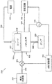
[0063] 圧力の変化はヘリウムイオンプラズマの密度に影響を与える一方、カソード518にて発生された二次的電子フィールドの密度に影響を与えるため、室513内の実際の気体圧力を監視する手段を設けることができる。弁521を適切に調節することにより、囲い物513内にて初期圧力を設定することができる。カチオンを保持するプラズマがプラズマ領域514内にて生成されたとき、室513内の瞬間的な静圧力を間接的に監視するため電圧モニター装置550を設けることができる。電圧の上昇は室の圧力が低いことを示す。電圧モニター装置550の出力信号を使用して、弁コントローラ552を通じて弁521を制御する。制御装置548によりワイヤー電極516に供給される電流は、また、電圧モニター装置550の信号により制御される。気体供給弁521及び制御装置548を制御すべく電圧モニター装置550によって発生された信号を利用することは、エミッタ510からの電子フィールドの出力を安定化させることを可能にする。
[0063] Means for monitoring the actual gas pressure in the
[0064] エミッタ510により発生された電流は、カソード518にぶつかるカチオンの密度により測定することができる。カソード518にぶつかるカチオンの密度は、制御装置548を通してワイヤー電極516の電圧を調節することにより制御することができる。カソード518から放出される電子のエネルギは、電源522を通してカソード518の電圧を調節することにより制御することができる。放出された電子の電流及びエネルギの双方は、独立的に制御し、これらのパラメータと印加された電圧との間の関係は線形であり、エミッタ510の制御を効率的で、且つ効果的なものにする。これに反して、従来の熱イオン電子ビーム銃は、ビームのパラメータを調節するとき、相応する線形の仕方にて制御することはできない。
[0064] The current generated by the
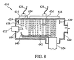
[0065] 図8は、本発明に従った電子ビーム溶融炉の1つの実施の形態の概略図であり、炉610は、全体として、図6及び図7に示し、且つこれの図面に関して上述したような設計を有する2つのワイヤー放電イオンプラズマ電子エミッタ614、616を組み込んでいる。炉610は、真空室620と、材料の供給装置622と、鋳造装置又は噴霧装置624とを含んでいる。上述したように、エミッタ614、616が作動するのに必要な電流は、電力線626によりエミッタに供給され、エミッタ614、616と真空室620との間の相互接続部は電子透過性フォイル窓部634、636を有しており、該窓部は、エミッタ614、616により発生された電子フィールド538が真空室620に入るのを許容する。エミッタ614、616内の作動圧力及び真空室内の作動圧力が同一又は実質的に相違しない場合、フォイル窓部634、636を省略することができる。電子フィールド638を磁気的にステアする手段639を真空室620内に含め、更なる工程の制御を行うことができる。例えば、冷間炉とすることのできる炉床640が真空室620内に配置されている。作動時、ワイヤー放電イオンプラズマ電子エミッタ614、616は励起され、且つ電子フィールド618を発生させる。導電性の供給材料644が供給装置622により真空室620内に導入され、エミッタ614から放出された電子フィールド638によって溶融されて炉床640に落下する。エミッタ616により発生された広い面積の電子フィールド638は、炉床640内に滞在する間、溶融材料642を加熱し、ガス抜きし、且つ精製する。溶融材料642は、炉床640に沿って前進し、且つ鋳造装置又は噴霧装置624内に落下し、所望の形態に加工される。
[0065] FIG. 8 is a schematic diagram of one embodiment of an electron beam melting furnace in accordance with the present invention, the
[0066] 例えば、本発明の上述したワイヤー放電イオンプラズマ電子エミッタのような、イオンプラズマ電子エミッタの色々な非限定的な実施の形態は、従来の熱イオン電子ビーム銃よりも高い真空圧力にて作動することができる。溶融炉をこれらの高い圧力にて作動させることは、上記に更に詳細に説明したように、溶融する材料内の揮発性成分の気化を減少させることができる。しかし、これらの揮発性成分の任意のものが溶融炉内にて高い蒸気圧力状態下にてさえ、溶融材料から沸騰し、溶融炉の比較的冷間の室の壁に凝縮する場合、形成された凝縮物は、室の壁から剥がれ、溶融体中に落下する。溶融体中に落下する凝縮物は、溶融体を介入物にて汚染させ、且つ(又は)溶融体の化学的性質に局所的変化を生じさせる。当該発明者は、イオンプラズマ電子エミッタ溶融炉及びその他の型式の溶融炉内にてかかる凝縮物の形成を防止し又は阻止する装置及び方法を開発することが有益であろうことを知った。 [0066] Various non-limiting embodiments of ion plasma electron emitters, such as, for example, the wire discharge ion plasma electron emitter of the present invention described above, are at higher vacuum pressures than conventional thermionic electron beam guns. Can be operated. Operating the melting furnace at these high pressures can reduce the evaporation of volatile components in the material to be melted, as described in more detail above. However, any of these volatile components are formed if they boil from the molten material and condense on the relatively cold chamber walls of the melting furnace, even under high steam pressure conditions in the melting furnace. The condensate that peels off the chamber walls and falls into the melt. Condensate falling into the melt can contaminate the melt with the intervention and / or cause local changes in the chemistry of the melt. The inventor has realized that it would be beneficial to develop an apparatus and method for preventing or preventing the formation of such condensates in ion plasma electron emitter melting furnaces and other types of melting furnaces.
[0067] 従って、本発明は、一部分、イオンプラズマ電子エミッタの形態とされた少なくとも1つの補助電子エミッタを含む装置に関するものであり、これは、例えば、導電性の金属材料を溶融させるため、ワイヤー放電イオンプラズマ電子エミッタのような、2つ以上のイオンプラズマ電子エミッタを備える溶融炉と共に使用する構成とされたワイヤー放電イオンプラズマ電子エミッタのようなものである。本発明に従った別の非限定的な実施の形態は、例えば、2つ以上の熱イオン電子ビーム銃及び(又は)その他の溶融装置を備える溶融炉と共に使用する構成とされた補助ワイヤー放電イオンプラズマ電子エミッタのような、イオンプラズマエミッタの形態をした少なくとも1つの補助電子エミッタを含む装置に関する。本発明に従った補助電子エミッタは、電子源としてイオンプラズマ電子エミッタを備えているため、これは、本明細書にて補助イオンプラズマ電子エミッタ、補助電子エミッタとして、又は一例としての実施の形態にて補助ワイヤー放電イオンプラズマ電子エミッタと称する。当業者は、本明細書を検討したとき、本明細書にてワイヤー放電イオンプラズマ電子エミッタ及び補助ワイヤー放電イオンプラズマ電子エミッタについて詳細に説明したが、任意のその他の適当なイオンプラズマ電子エミッタ又は補助イオンプラズマ電子エミッタを使用することができ、且つこれは、本発明の範囲に属するものであることが認識されよう。その他の適当なイオンプラズマ電子エミッタ及びその他の適当な補助イオンプラズマ電子エミッタの例については、以下に更に詳細に説明する。更に、以下に説明するように、ワイヤー放電イオンプラズマ電子エミッタ及び補助ワイヤー放電イオンプラズマ電子エミッタの「ワイヤー」は、例えば、円形、線形、四角形、矩形、長円形、楕円形、又は三角形の形状のような任意の適当な形状に形成し、色々な形状の断面積又は外形を有する電子フィールドを形成することができる。 [0067] Accordingly, the present invention relates to an apparatus that includes at least one auxiliary electron emitter, partially in the form of an ion plasma electron emitter, which includes, for example, a wire to melt a conductive metal material. Such as a wire discharge ion plasma electron emitter configured for use with a melting furnace comprising two or more ion plasma electron emitters, such as a discharge ion plasma electron emitter. Another non-limiting embodiment according to the present invention is for example auxiliary wire discharge ions configured for use with a melting furnace comprising two or more thermionic electron beam guns and / or other melting devices. The invention relates to a device comprising at least one auxiliary electron emitter in the form of an ion plasma emitter, such as a plasma electron emitter. Since the auxiliary electron emitter according to the invention comprises an ion plasma electron emitter as an electron source, this is referred to herein as an auxiliary ion plasma electron emitter, as an auxiliary electron emitter, or in an exemplary embodiment. This is called an auxiliary wire discharge ion plasma electron emitter. While those skilled in the art have discussed in detail herein wire discharge ion plasma electron emitters and auxiliary wire discharge ion plasma electron emitters when reviewing this specification, any other suitable ion plasma electron emitter or auxiliary It will be appreciated that ion plasma electron emitters can be used and are within the scope of the present invention. Examples of other suitable ion plasma electron emitters and other suitable auxiliary ion plasma electron emitters are described in further detail below. Further, as described below, the “wire” of the wire discharge ion plasma electron emitter and the auxiliary wire discharge ion plasma electron emitter can be, for example, circular, linear, square, rectangular, oval, elliptical, or triangular in shape. In any suitable shape, an electronic field having various shapes of cross-sectional areas or outer shapes can be formed.
[0068] 特定の非限定的な実施の形態において、本発明に従った補助電子ビームエミッタは、上述した色々なワイヤー放電イオンプラズマ電子エミッタと同一又は類似の仕方にて構成され、且つ機能するワイヤー放電イオンプラズマ電子エミッタを備えることができる。例えば、補助ワイヤー放電イオンプラズマ電子エミッタは、陽イオンを含むプラズマを作り出す構成とされた細長いワイヤーアノードと、カソードを負にて帯電させる構成とされた高電圧の電源と電気的に接続されたカソードを含むカソード領域とを備えることができる。色々な非限定的な実施の形態において、カソードは、ワイヤー電極に対して位置決めされ、ワイヤー電極により発生された陽イオンがカソードに向けて加速され、且つカソードに衝突し、カソードから電子を解放し、且つ例えば、収束した電子フィールドのような電子フィールドを作り出すことができる。収束した電子フィールドは、例えば、電磁石を使用することにより電磁的に「収束させ」且つ(又は)溶融室の適当な領域に向けることができる。本明細書の目的上、「収束した電子フィールド」という語は、少なくとも電磁的に収束された後、上述した色々なイオンプラズマ電子エミッタにより放出された電子フィールドの断面積(以下、「広い面積の電子フィールド」と呼ぶ)よりも小さい断面積を有するフィールドを意味する。電子フィールドの収束は、例えば、単位面積当たりより大きい電子密度を提供することにより、電子フィールドをより高電力にて作動させることができる。本明細書にて電子フィールドの「断面積」又は「断面外形」に言及するとき、断面積は、時間の特定の時点にて色々な電子フィールドの移動路に対し実質的に垂直な方向をとることを理解すべきである。 [0068] In certain non-limiting embodiments, the auxiliary electron beam emitter according to the present invention is configured and functions in the same or similar manner as the various wire discharge ion plasma electron emitters described above. A discharge ion plasma electron emitter can be provided. For example, an auxiliary wire discharge ion plasma electron emitter is an elongated wire anode configured to create a plasma containing positive ions, and a cathode electrically connected to a high voltage power source configured to negatively charge the cathode. And a cathode region containing. In various non-limiting embodiments, the cathode is positioned relative to the wire electrode, and the cations generated by the wire electrode are accelerated towards the cathode and collide with the cathode, releasing electrons from the cathode. And, for example, an electronic field such as a converged electronic field can be created. The converged electron field can be “converged” electromagnetically and / or directed to an appropriate region of the melting chamber, for example, by using an electromagnet. For the purposes of this specification, the term “focused electron field” refers to the cross-sectional area (hereinafter “wide area”) of the electron field emitted by the various ion plasma electron emitters described above after being at least electromagnetically focused. This means a field having a smaller cross-sectional area than that of an electronic field. Convergence of the electron field can operate the electron field at higher power, for example, by providing a higher electron density per unit area. As used herein, when referring to the “cross-sectional area” or “cross-sectional outline” of an electronic field, the cross-sectional area takes a direction that is substantially perpendicular to the path of movement of the various electronic fields at a particular point in time. You should understand that.
[0069] 特定の非限定的な実施の形態において、補助ワイヤー放電イオンプラズマ電子エミッタは、上述した、色々なワイヤー放電イオンプラズマ電子エミッタにより発生された低電力、低密度及び非収束の電子フィールドと比較したとき、上述した色々なワイヤー放電イオンプラズマ電子エミッタよりも高電力にて作動し、高電力、高い電子密度、及び(又は)収束した電子フィールドを提供することができる。一例としての実施の形態において、カソードがより高い負電圧に帯電され、次に、電子フィールドの電子エネルギは、カソードから出る自由電子の電子エネルギが大きいため、一層大きくなるであろう。更に、アノードにより高い電圧が印加された場合、アノードにて作り出されるイオンが多量であるから、電子フィールドの電子密度は一層大きくなるであろう。別の一例としての実施の形態において、アノード及びカソード(負の電圧)の双方に高い電圧を印加し、より大きいエネルギで且つ高密度の電子フィールドを作り出すことができる。次に、この電子フィールドは、電磁的に収束させ且つ(又は)溶融体の一部分に向けることができる。従って、かかる実施の形態の収束した電子フィールドを使用して凝縮物、溶融体中の凝縮物、溶融体中の凝固部分、及び(又は)例えば、溶融体中の非溶融部分を溶融させることができる。収束した電子フィールドを使用して、真空室の色々な領域にて溶融炉の真空室内の溶融材料を適当な温度に維持することができる。凝縮物、凝固部分、及び(又は)溶融体中の非溶融部分が真空室の領域内に滞在する時間が短いため、より高エネルギ、高密度、及び(又は)より収束した電子フィールドを使用することができる。従って、凝縮物、凝固部分、及び(又は)非溶融部分を真空室の別の領域内に移動する前、溶融させることが望ましい。補助ワイヤー放電イオンプラズマ電子エミッタは、ステア可能にし、補助電子エミッタにより発生された収束した電子フィールドの方向は、例えば、溶融炉の真空室内の任意のその他の適当な領域に動かし、且つ(又は)向けることができ、その収束した電子フィールドが形成し又は凝固するインゴットの1つの領域に衝突するようにすることができる。1つの非限定的な実施の形態において、収束した電子フィールドは、形成し又は凝固するインゴットの領域に衝突し、溶融プール231の凝固動力学に、従って、例えば、固体インゴット232の特徴に有益な影響を与えることができる。
[0069] In certain non-limiting embodiments, the auxiliary wire discharge ion plasma electron emitter includes the low power, low density and unfocused electron fields generated by the various wire discharge ion plasma electron emitters described above. When compared, it can operate at a higher power than the various wire discharge ion plasma electron emitters described above, providing a higher power, higher electron density, and / or a converged electron field. In an exemplary embodiment, the cathode is charged to a higher negative voltage, and then the electron energy of the electron field will be higher due to the higher free electron energy from the cathode. In addition, when a higher voltage is applied to the anode, the electron density in the electron field will be higher because of the greater amount of ions created at the anode. In another exemplary embodiment, a higher voltage can be applied to both the anode and cathode (negative voltage) to create a higher energy and higher density electronic field. This electronic field can then be electromagnetically focused and / or directed to a portion of the melt. Accordingly, the converged electron field of such embodiments may be used to melt the condensate, the condensate in the melt, the solidified portion in the melt, and / or, for example, the non-molten portion in the melt. it can. Using the converged electron field, the molten material in the vacuum chamber of the melting furnace can be maintained at an appropriate temperature in various regions of the vacuum chamber. Use higher energy, higher density, and / or a more focused electron field due to the short time that condensate, solidified part, and / or non-molten part in the melt stay in the region of the vacuum chamber be able to. Therefore, it is desirable to melt the condensate, the solidified part, and / or the non-molten part before moving it into another area of the vacuum chamber. The auxiliary wire discharge ion plasma electron emitter is steerable and the direction of the focused electron field generated by the auxiliary electron emitter is moved to, for example, any other suitable region within the vacuum chamber of the melting furnace, and / or Can be directed so that its converged electron field impacts one region of the ingot that forms or solidifies. In one non-limiting embodiment, the converged electron field impacts the region of the ingot that forms or solidifies, which is beneficial to the solidification kinetics of the
[0070] 当業者は、本発明の補助ワイヤー放電イオンプラズマ電子エミッタは、例えば、上述した色々なワイヤー放電イオンプラズマ電子エミッタの適当な特徴を備えることができることが認識されよう。従って、また、簡略化のため、これらの特徴は、補助ワイヤー放電イオンプラズマ電子エミッタに関してこの部分にて特定的に言及はしない。上述した図1−8の任意の構成要素、要素及び(又は)部分と同一の番号を付した図9−15の任意の構成要素、要素及び(又は)部分は、同一の又は類似のものとし、且つ同一の又は類似の構成及び(又は)機能を有することができる。また、図1−8に示した色々な一例としての実施の形態に関して上述した任意の構成要素、要素及び(又は)部分は、図9−15にて説明した色々な一例としての実施の形態と共に使用することができる。 [0070] Those skilled in the art will recognize that the auxiliary wire discharge ion plasma electron emitter of the present invention can include suitable features of, for example, the various wire discharge ion plasma electron emitters described above. Therefore, also for simplicity, these features are not specifically mentioned in this part with respect to the auxiliary wire discharge ion plasma electron emitter. Any of the components, elements and / or portions of FIGS. 9-15 labeled with the same numbers as any of the components, elements and / or portions of FIGS. 1-8 described above shall be the same or similar. And having the same or similar configuration and / or function. Also, any of the components, elements and / or portions described above with respect to the various exemplary embodiments shown in FIGS. 1-8 may be combined with the various exemplary embodiments described in FIGS. 9-15. Can be used.
[0071] 1つの非限定的な実施の形態において、図9を参照すると、補助ワイヤー放電イオンプラズマ電子エミッタ700は、溶融炉210の真空室214内に又は該真空室に隣接して位置決めすることができる。該補助ワイヤー放電イオンプラズマ電子エミッタ700は、2つ以上のワイヤー放電イオンプラズマ電子エミッタ216と共に又は独立的に使用することができる。1つの非限定的な実施の形態において、2つ以上のワイヤー放電イオンプラズマ電子エミッタ216を使用して、金属材料のバー220を加熱し、且つ溶融させることができ、また、2つ以上のワイヤー放電イオンプラズマ電子エミッタ216を使用して炉床224内の溶融金属材料226を加熱し、且つ精製することができる。特定の非限定的な実施の形態において、補助ワイヤー放電イオンプラズマ電子エミッタ700を使用し、真空室214の壁215上に形成された任意の凝縮物、及び(又は)炉床224内に存在する溶融金属材料中の凝縮物を含む任意の凝固部分を溶融させることができる。その他の非限定的な実施の形態において、補助ワイヤー放電イオンプラズマ電子エミッタを使用して、本明細書にて説明したように、形成し又は凝固するインゴット232の溶融プール231又はその他の領域を加熱することができる。
[0071] In one non-limiting embodiment, referring to FIG. 9, the auxiliary wire discharge ion
[0072] 従って、色々な非限定的な実施の形態において、補助ワイヤー放電イオンプラズマ電子エミッタ700は、室の壁215上に形成された凝縮物を選択的に溶融させ、これにより、固体の凝縮物が室の壁215から剥がれ、且つ溶融した材料226内に落下する可能性を防止し又は少なくし得るようにすることができる。また、色々な非限定的な実施の形態において、補助ワイヤー放電イオンプラズマ電子エミッタ700は、例えば、炉床224に沿った所望の領域を更に加熱し、例えば、溶融材料226中の凝縮物のような、固体を溶融させ、且つ(又は)炉床224に沿った2つ以上の領域にて溶融材料226を溶融状態に維持し得るようにすることができる。更に、色々な非限定的な実施の形態において、補助ワイヤー放電イオンプラズマ電子エミッタ700は、溶融プール231の領域を加熱し、且つ溶融プール231の凝固動力学及びインゴット232の特徴に有益に影響を与え得るようにすることができる。補助ワイヤー放電イオンプラズマ電子エミッタ700により放出された収束した電子フィールドを溶融プール231に印加することは、引き抜く間、インゴット232の表面仕上げを改良し、インゴット232内の金属の引裂きを最小にし、且つ(又は)例えば、インゴット232の形成される微細構造に有益な影響を与えることができる。
[0072] Accordingly, in various non-limiting embodiments, the auxiliary wire discharge ion
[0073] 1つの非限定的な実施の形態において、図9を更に参照すると、該補助ワイヤー放電イオンプラズマ電子エミッタ700は、例えば、収束した電子フィールド702のような、収束した電子フィールドを作り出す構成とされている。この収束した電子フィールド702は,三次元的電子フィールドであり、このため、標的に衝突するとき、従来の熱イオン電子ビーム銃により発生された実質的に線形の電子「ビーム」よりも遥かに大きい領域を包含する。しかし、該収束した電子フィールド702は、例えば、上述したように、ワイヤー放電イオンプラズマ電子エミッタ216により放出された、比較的広い面積の電子フィールド218により包含される領域よりも小さく又は遥かに小さい面積を有する領域を包含することができる。1つの非限定的な実施の形態において、収束した電子フィールド702は、溶融炉の真空室内にて標的に衝突するとき、例えば、3.22cm2(0.5inch2)から322.58cm2(50inch2)、代替的に、6.45cm2(1inch2)から193.54cm2(30inch2)、代替的に、6.45cm2(1inch2)から129.03cm2(20inch2)の面積を有することができる。収束した電子ビームは、特定の実施の形態において、該ビームが凝縮物又は溶融体内のその他の固体部分と衝突することができるようにステア可能又は少なくとも方向決め可能である。当業者は、本発明を検討したとき、収束した電子フィールドは、特定の用途にあった任意の適当な断面積又は外形を有することができることが認識されよう。
[0073] In one non-limiting embodiment, and with further reference to FIG. 9, the auxiliary wire discharge ion
[0074] 1つの非限定的な実施の形態において、収束した電子フィールド702の断面積及び(又は)断面形状は、例えば、補助電子エミッタのアノード及びカソードの寸法及び形状の関数とすることができる。例えば、特定の非限定的な実施の形態において、アノード及びカソードは、比較的大きい寸法のものとし、また、収束した電子フィールド702は、比較的大きい断面積を包含するものとする。しかし、この相対的に大きい断面積は、全体として、広い面積の電子フィールドの断面積よりは小さいが、従来の熱イオン電子エミッタにより放出された実質的に線形の「ビーム」の実質的に「スポット」の包含範囲よりは実質的に大きい。この収束した電子フィールドは、また、例えば、アノードの形状に基づく円形又は四角形のような、色々な断面形状を有するようにしてもよい。1つの非限定的な実施の形態において、カソードと共に、円形の形状を有するアノードを使用し、例えば、円形又は実質的に円形の断面形状を有する収束した電子フィールドを作り出すことができる。
[0074] In one non-limiting embodiment, the cross-sectional area and / or cross-sectional shape of the
[0075] 1つの非限定的な実施の形態において、図9を再度参照すると、ワイヤー放電イオンプラズマ電子エミッタ216は、第一の断面積を有する少なくとも1つの第一の電子フィールド218(すなわち、広い面積のフィールド)を放出することができる。補助ワイヤー放電イオンプラズマ電子エミッタ700は、第二の断面積を有する収束した電子フィールド702のような、第二の電子フィールドを放出することができる。色々な実施の形態において、第一の断面積は、第二の断面積よりも大きくし、同一又はより小さくすることができる。特定の電子フィールドが凝縮物、溶融材料中の固体部分、形成し又は凝固するインゴットの領域、及び(又は)真空室のその他の領域に衝突したとき、電子フィールドが包含する面積を意味するものとする。
[0075] In one non-limiting embodiment, referring again to FIG. 9, the wire discharge ion
[0076] 1つの非限定的な実施の形態において、補助ワイヤー放電イオンプラズマ電子エミッタ700により放出された収束した電子フィールド702は、ワイヤー放電イオンプラズマ電子エミッタ216により放出された広い面積の電子フィールドよりも小さい断面積を有している。当該実施の形態において、収束した電子フィールド702は、ワイヤー放電イオンプラズマ電子エミッタ216により放出された広い面積の電子フィールドよりも収束させ且つ選択的により高電力(例えば、より高い電子密度及び(又は)より高エネルギの電子)であるようにすることができる。収束した電子フィールド702の高い電子密度は、アノードに対しより高電圧を印加して、例えば、アノードにてより多くのイオンを作り出し、このため、カソードから来るより多くの二次的電子を作り出すことにより形成することができる。収束した電子フィールド702の電力は、増大又は減少させて、溶融体の凝縮物又は固体部分を適当に溶融させることができる。かかる1つの実施の形態において、カソードの電子の加速電圧(kV)、及び電子の電流(kW)は、例えば、適当に溶融させるよう変化させることができる。1つの非限定的な実施の形態において、電子の電流(kW)を増大させ、より迅速な溶融を生じさせることができる。その他の非限定的な実施の形態において、収束した電子フィールド702を更に収束させ、収束した電子フィールド702内の電子の密度を増し、これにより、より迅速な溶融を生じさせることもできる。
[0076] In one non-limiting embodiment, the
[0077] 1つの非限定的な実施の形態において、収束した電子フィールド702は、溶融合金226又は溶融プール231内の任意の凝縮物、凝固した部分及び(又は)非溶融部分に向けることができる。更に、特定の実施の形態において、収束した電子フィールド702は、溶融プール231に向け、溶融材料がインゴット232に凝固する状態に影響を与えることができる。また、収束した電子フィールド702は、凝縮物を有する室の壁215の領域に向け、溶融炉210の凝縮物又はその他の領域を溶融させることができる。
[0077] In one non-limiting embodiment, the focused
[0078] 図9を再度、参照すると、収束した電子フィールド702は、例えば、ステアリングシステム704のようなステアリングシステムにより向けることもできる。該ステアリングシステム704は、例えば、2つ以上の電子フィールド及び(又は)磁界を発生させ、且つ操作して収束した電子フィールド702をステアし、その電子フィールドを溶融炉210の真空室214内の所望の領域に又は物に衝突させることができる。例えば、磁気偏向のような、電子フィールドの方向の操作のため、当業者に知られた従来の技術及び装置は、ステアリングシステム704内にて適当に使用し得るようにすることができる。電子フィールドを操作する技術及び装置は、当業者に知られていることを考えて、これらについて本明細書にて詳細には説明しない。また、例えば、ステアリングシステム704は、補助ワイヤー放電イオンプラズマ電子エミッタ700により発生された収束した電子フィールド702を溶融炉210の真空室214内の特定の領域の回りにて選択的にラスター走査する設計とすることができる。電子ビームをラスター走査するため、当業者に知られた色々な従来の技術及び装置は、ステアリングシステム704にて適当に使用し得るようにすることができる。電子フィールドをラスター走査するかかる技術及び装置は当業者に知られていることを考慮して、これらについて本明細書にて詳細には説明しない。1つの非限定的な実施の形態において、収束した電子フィールド702をラスター走査することは、フィールドを室の壁215上の凝縮材料の領域上にて迅速に動かし、炉床224内にて材料の凝固部分又は非溶融部分上にて凝縮体を溶融させ、材料を溶融させ且つ(又は)溶融プール231上にて材料を溶融させ、形成されるインゴット232の凝固に所望通りの影響を与えることができる。また、収束した電子フィールド702のラスター走査を採用して余分な電力又はエネルギが収束した電子フィールド702により凝縮体、凝固部分、及び(又は)収束したフィールド702が衝突する溶融材料に伝送される可能性を無くし、又は少なくとも減少させるのを助けることができる。余分なエネルギ/単位面積及び(又は)電子密度/単位面積を凝縮体、凝固部分、及び(又は)溶融材料に加えることは、凝縮体又は材料中の揮発性成分を気化させ、このことは、室の壁215上への材料の凝縮を悪化させる可能性がある。1つの非限定的な実施の形態において、ステアリングシステム704を使用して収束した電子フィールド702を溶融炉210内の任意の適当な位置に向けることができる。
[0078] Referring again to FIG. 9, the converged
[0079] 1つの非限定的な実施の形態において、収束した電子フィールド702に対するステアリングシステムは、選択的に作動させ、操作者が収束した電子フィールド702を溶融及び(又は)再加熱を必要とする溶融体の特定の部分に特定的に向けることができるようにする。かかる選択的なステアリングシステムは、ステアリング装置704又はその他のステアリング装置を移動させ、これにより収束した電子フィールド702を溶融体中の凝縮物の粒子上のような、真空室内の適当な領域に向けることができる。その他の非限定的な実施の形態において、例えば、電磁石のような色々なステアリング装置を真空室内にて適正に配列し、収束した電子フィールド702を真空室の所定の領域に向けることができ、且つ(又は)操作者によって、例えば、真空室の第一の所定の領域と真空室の第二の所定の領域との間にて選択的に移動させることができる。
[0079] In one non-limiting embodiment, the steering system for the converged
[0080] 図10には、例えば、電子ビーム溶融炉610内に含めたワイヤー放電イオンプラズマ電子エミッタのような、補助イオンプラズマ電子エミッタ700´の別の非限定的な実施の形態が示されている。電子ビーム溶融炉610の色々な要素は、図8に含め且つ上述したように、参照番号により識別されている。補助イオンプラズマ電子エミッタ700´は、収束した電子フィールド700に類似した収束した電子フィールド702´を放出し、この電子フィールドは、炉床640内に配置された溶融材料642及び(又は)溶融材料642中の固体(例えば、室の壁から落下した凝縮物)に衝突するようにすることができる。1つの非限定的な実施の形態において、補助イオンプラズマ電子エミッタ700´は、例えば、上述した構造を有することのできるステアリングシステム704´を含むことができる。
[0080] FIG. 10 illustrates another non-limiting embodiment of an auxiliary ion plasma electron emitter 700 ', such as, for example, a wire discharge ion plasma electron emitter included in an electron
[0081] 図11に概略図で示した1つの非限定的な実施の形態において、一例としてのステアリングシステムは、補助イオンプラズマ電子エミッタ700又は700´(全体的に「700」にて表示)と共に使用し得るようにされている。補助イオンプラズマ電子エミッタ700の収束した電子フィールド702用のステアリングシステムは、第一の磁気及び(又は)電気ステアリング装置706と、第二の磁気及び(又は)電気ステアリング装置708とを備えることができる。第一のステアリング装置706を、収束した電子フィールド702の第一の側部に配置し、第二のステアリング装置708を収束した電子フィールド702の第二の側部に配置することができる。第一及び第二のステアリング装置706、708は、収束した電子フィールド702を所望の方向に向けるよう変換可能な磁界及び(又は)電界をその間にて発生させる構成とすることができる。その結果、第一及び第二のステアリング装置706、708を使用して収束した電子フィールド702を溶融炉の真空室の所望の領域又は位置に向けることができる。ステアリングシステムは、追加的なステアリング装置を含み、収束した電子フィールド702を、真空室内の任意の適当な方向に向けることができる。図11に示した一例としてのステアリングシステムを使用して、収束した電子フィールド702を収束させ又は更に収束させることができる。
[0081] In one non-limiting embodiment, shown schematically in FIG. 11, an exemplary steering system may be used with an auxiliary ion
[0082] 収束した電子フィールド702用のステアリングシステムの別の非限定的な実施の形態が図12に概略図で示されている。かかる1つの実施の形態において、ステアリングシステムは、収束した電子フィールド702(図12に図示しないが、図面に対し全体的に垂直に経路内に突き出している)の回りに位置決めされた2つ以上のステアリング装置710を備えることができる。上記の第一及び第二のステアリング装置706、708と類似して、ステアリング装置710は、収束した電子フィールド702に作用する構成とされた磁界及び(又は)電界を各々発生させることができる。例えば、2つ以上、3つ以上又は4つ以上のステアリング装置710を提供することにより、収束した電子フィールド702は、溶融炉の真空室内の任意の所望の領域又は物に正確に向けることができる。当業者は、電子フィールドをステアリングするためのその他の従来のシステムを本明細書にて上述した補助イオンプラズマ電子エミッタと共に使用して収束した電子フィールド702の方向をステアすることができることが認識されよう。図11の一例としてのステアリングシステムに類似して、図12の一例としてのステアリングシステムを使用して、電子フィールド702を収束し又はその収束した電子フィールドを更に収束することもできる。
[0082] Another non-limiting embodiment of a steering system for a converged
[0083] 1つの非限定的な実施の形態において、導電性の金属材料の溶融装置は、第一の形状を有する断面外形を含む収束した電子フィールドを作り出す構成とされた補助ワイヤー放電イオンプラズマ電子エミッタと、収束した電子フィールドを向けて導電性の金属材料の少なくとも一部分に衝突させ、任意の固体の凝縮体又はその他の固体を溶融させる構成とされたステアリングシステムとを備えることができる。収束した電子フィールドを、ステアリングシステムによって溶融プール、又は形成し又は凝固するインゴットのその他の領域に向け、インゴットの凝固動力学に有益な影響を与えることもできる。かかる非限定的な実施の形態において、該装置は、第二の形状を有するワイヤー電極と、第三の形状を有するカソードとを備えることができる。少なくとも1つの実施の形態において、第一の形状は、第二の形状及び(又は)第三の形状に実質的に類似し又は同一のものとすることができる。電子フィールドの断面外形の第一の形状は、例えば実質的に円形、三角形、矩形、四角形、長円形又は楕円形の形状とし、又は、任意のその他の適当な形状とすることができる。このように、当業者は、収束した電子フィールドの断面外形の第一の形状は、凝縮物の溶融、溶融体中の固体の溶融、溶融体中の金属材料の非溶融部分の溶融、及び(又は)凝固するインゴットの溶融プールを所望の仕方にて加熱するのに適した任意の形状とすることができることが認識されよう。例えば、実質的に三角形の断面外形を有する収束した電子フィールドが所望である場合、補助ワイヤー放電イオンプラズマ電子エミッタは、実質的に三角形のワイヤー電極及び(又は)実質的に三角形のカソードを含むことができる。 [0083] In one non-limiting embodiment, a conductive metal material melting apparatus is configured to produce a focused electron field that includes a cross-sectional profile having a first shape. An emitter and a steering system configured to cause the focused electron field to impinge on at least a portion of the conductive metallic material and to melt any solid condensate or other solids. The focused electronic field can also be directed to a molten pool or other region of the ingot that forms or solidifies by the steering system, which has a beneficial effect on the solidification dynamics of the ingot. In such a non-limiting embodiment, the device can comprise a wire electrode having a second shape and a cathode having a third shape. In at least one embodiment, the first shape can be substantially similar or identical to the second shape and / or the third shape. The first shape of the cross-sectional profile of the electronic field can be, for example, a substantially circular, triangular, rectangular, square, oval or elliptical shape, or any other suitable shape. Thus, those skilled in the art will appreciate that the first shape of the cross-sectional profile of the converged electron field is the melting of the condensate, the melting of the solid in the melt, the melting of the unmelted portion of the metallic material in the melt, and ( It will be appreciated that the molten pool of solidified ingots can be any shape suitable for heating in a desired manner. For example, if a focused electron field having a substantially triangular cross-sectional profile is desired, the auxiliary wire discharge ion plasma electron emitter includes a substantially triangular wire electrode and / or a substantially triangular cathode. Can do.
[0084] 1つの非限定的な実施の形態において、イオンプラズマ電子エミッタ又は補助イオンプラズマ電子エミッタは、ワイヤー状のアノード以外のアノード(又はカチオンを作り出す電極)を備えることができる。かかる1つの実施の形態において、アノードは、カソードから放出された収束した電子フィールドが容易に通過するのを許容する構成とされた導電性の薄い板、シート又はフォイルとすることができる。その他の実施の形態において、アノードは、任意のその他の適当な構成のものとすることができる。導電性の薄い板、シート又はフォイルアノードは、実質的に円形、四角形、矩形、三角形、長円形、楕円形又は任意のその他の適当な形状のような任意の適当な形状を有するものとすることができる。これら色々な形状又はその他の形状にてアノードを提供することにより、断面積の形状又は広い面積の電子フィールド及び(又は)収束した電子フィールドの外形を制御することができる。例えば、円形の断面形状を有する収束した電子フィールドを作り出すため、円形の薄い板、シート又はフォイルアノードを使用することができる。1つの非限定的な実施の形態において、イオンプラズマ電子エミッタ又は補助イオンプラズマ電子エミッタのカソードは、任意の適当な寸法を有する任意の導電性の薄い板、シート又はフォイルから成るものとすることができる。この導電性の薄い板、シート又はカソードのフォイルは、上述した色々なアノードの形状と類似した形状を有することができる。1つの非限定的な実施の形態において、カソードの形状は、アノードの形状と共に作用し、色々な形状の断面積又は外形を有する広い面積の電子フィールド又は収束した電子フィールドを作り出すことができる。広い面積の電子フィールドを作り出すイオンプラズマ電子エミッタは、一例としてのワイヤー放電イオンプラズマ電子エミッタに関して上述したが、当業者は、「ワイヤー無し」又は「非直線状ワイヤ」アノードを有するイオンプラズマ電子エミッタを使用することができ、これは、本発明の範囲に属することが認識されよう。 [0084] In one non-limiting embodiment, an ion plasma electron emitter or an auxiliary ion plasma electron emitter can comprise an anode (or electrode that produces cations) other than a wire-like anode. In one such embodiment, the anode can be a thin conductive plate, sheet or foil that is configured to allow a focused electron field emitted from the cathode to pass easily. In other embodiments, the anode can be of any other suitable configuration. The conductive thin plate, sheet or foil anode shall have any suitable shape, such as a substantially circular, square, rectangular, triangular, oval, elliptical or any other suitable shape. Can do. By providing the anode in these various or other shapes, it is possible to control the cross-sectional shape or large area electron field and / or the outer shape of the converged electron field. For example, a circular thin plate, sheet or foil anode can be used to create a focused electron field having a circular cross-sectional shape. In one non-limiting embodiment, the cathode of an ion plasma electron emitter or an auxiliary ion plasma electron emitter may consist of any conductive thin plate, sheet or foil having any suitable dimensions. it can. The conductive thin plate, sheet or cathode foil may have a shape similar to the various anode shapes described above. In one non-limiting embodiment, the shape of the cathode can work with the shape of the anode to create a large area or convergent electron field with various shapes of cross-sectional areas or profiles. While ion plasma electron emitters that produce large area electron fields have been described above with respect to exemplary wire discharge ion plasma electron emitters, those skilled in the art will recognize ion plasma electron emitters having “no wire” or “non-linear wire” anodes. It will be appreciated that this can be used and is within the scope of the present invention.
[0085] 上述した色々なワイヤー放電イオンプラズマ電子エミッタと類似して補助ワイヤー放電イオンプラズマ電子エミッタの色々な非限定的な実施の形態は、カチオンを保持するプラズマを作り出す構成とされた2つ以上の細長いワイヤーアノードを含むことができ、プラズマカチオンは、カソードに衝突し、二次的電子のフィールド(すなわち、収束した電子フィールド)を発生させ、このフィールドは、例えば、溶融体中の固体の介入物を減少させ得るように溶融させるべき、凝縮体のような、標的に衝突するよう加速させる。細長いワイヤーアノードは、その厚さ寸法よりも実質的に大きい長さ寸法を有することができる。「細長い」として説明したが、細長いワイヤーアノードは、任意の適当な形状に形成することができる。補助ワイヤー放電イオンプラズマ電子エミッタは、色々なワイヤー放電イオンプラズマ電子エミッタに関して上述したものと実質的に同一又は全体として類似した仕方の構造とすることができる。従って、色々なワイヤー放電イオンプラズマ電子エミッタの上記の説明は、補助ワイヤー放電イオンプラズマ電子エミッタの設計に関する本説明の一部とされている。更に、本発明による補助ワイヤー放電イオンプラズマ電子エミッタの特定の非限定的な実施の形態の構造及び作用の仕方について以下に説明する。 [0085] Similar to the various wire discharge ion plasma electron emitters described above, various non-limiting embodiments of auxiliary wire discharge ion plasma electron emitters are configured to produce plasma that retains cations. The plasma cation impinges on the cathode and generates a field of secondary electrons (ie, a focused electron field), which can be, for example, solid intervention in the melt Accelerate to collide with a target, such as a condensate, that should be melted so that things can be reduced. The elongated wire anode can have a length dimension that is substantially greater than its thickness dimension. Although described as “elongated”, the elongated wire anode can be formed into any suitable shape. The auxiliary wire discharge ion plasma electron emitter can be configured in a manner that is substantially the same or generally similar to that described above for the various wire discharge ion plasma electron emitters. Accordingly, the above description of various wire discharge ion plasma electron emitters is part of this description regarding the design of the auxiliary wire discharge ion plasma electron emitter. Furthermore, the structure and manner of operation of a particular non-limiting embodiment of an auxiliary wire discharge ion plasma electron emitter according to the present invention will be described below.
[0086] 上述したように、本発明に従った補助イオンプラズマ電子エミッタは、例えば、実質的に円形、四角形、矩形、三角形、長円形、又は楕円形の断面外形、又は任意のその他の適当な組み合わせた形状の別の断面外形のような、任意の適当な断面外形又は形状を有する収束した電子フィールドを作り出す構成とすることができる。特定の非限定的な実施の形態において、本発明に従った補助ワイヤー放電イオンプラズマ電子エミッタのような、補助イオンプラズマ電子エミッタは、実質的に矩形の形状の断面外形(図13及び図14参照)又は実質的に円形の断面外形(図15参照)を有する電子フィールドを発生させることができる。図13を参照すると、補助イオンプラズマ電子エミッタ802は、カチオンを保持するプラズマを作り出す構成とされたワイヤーアノード又は導電性の薄い板、シート又はフォイルアノード819(共に、819で表示)を含む、図4のプラズマ領域314と類似したイオン化領域又はプラズマ領域と、カソード818を含む、図4のカソード領域316に類似したカソード領域とを含むことができる。カソード818は、任意の適当な形状を有することができる。プラズマ領域は、イオン化可能な気体を低圧にて充填することができ、また、その気体は、プラズマ領域内にてイオン化し、カチオンを保持するプラズマを作り出すことができる。例えば、プラズマ領域は、例えば、約20ミルトルのヘリウム気体を充填することができる。細い直径のワイヤーアノード又は導電性の薄い板、シート又はフォイルアノード819をプラズマ領域内に配置することができる。このアノード819は、図13にて矩形の形状のものが示されているが、任意の適当な形状を有することができる。正の電圧を高電圧の電源822によりアノード819に印加し、ヘリウム気体をヘリウムカチオン及び自由な「一次的」電子を含むプラズマにイオン化することができる。ヘリウム気体のイオン化が開始されたならば、プラズマは、アノード819に電圧を印加することにより支えられる。プラズマ内の正に帯電したヘリウムイオンは、高い負電位に維持された、図4の引出し格子326と類似した引出し格子を通じてプラズマ領域から引き出され、且つ図4の高電圧の空隙328と類似した高い電圧空隙を通じてカソード領域内に加速され、このカソード領域にて、プラズマ内のカチオンは、高い負電圧に維持されたカソード818に衝撃する。カソード818は、例えば、被覆し又は非被覆の金属又は合金とすることができる。1つの非限定的な実施の形態において、カソード818は、高い溶融温度及び低い作用関数を有する挿入体から成るものとすることができる。図6の高電圧の電源522のような、高電圧の電源は、例えば、20,000ボルト以上の負電圧をカソード818に付与する。
[0086] As described above, the auxiliary ion plasma electron emitter according to the present invention can be, for example, a substantially circular, square, rectangular, triangular, oval, or elliptical cross-sectional profile, or any other suitable It can be configured to create a converged electronic field having any suitable cross-sectional profile or shape, such as another cross-sectional profile of the combined shape. In certain non-limiting embodiments, an auxiliary ion plasma electron emitter, such as an auxiliary wire discharge ion plasma electron emitter according to the present invention, has a substantially rectangular cross-sectional profile (see FIGS. 13 and 14). ) Or an electronic field having a substantially circular cross-sectional profile (see FIG. 15). Referring to FIG. 13, auxiliary ion
[0087] ヘリウムカチオンがカソード818に衝突すると、二次的電子はカソード818から解放され、これにより収束した電子フィールドを形成する。高電圧の空隙は、二次的電子をヘリウムカチオンの移動方向と反対の方向に加速し、引出し格子を通って、プラズマ領域(導電性の板、シート又はフォイル(存在するならば))を通り、次に、電子に対し相対的に透過性の材料にて出来た、図4の薄い金属フォイル窓部329に類似した薄い金属フォイル窓部(存在するならば)を通じて加速する。上述したように、補助電子エミッタ及び溶融炉の室内の相対的な気体圧力に依存して、電子透過性窓部を省略することが可能であり、この場合、補助電子エミッタにより作り出された電子は、直接、溶融炉の真空室に入るであろう。
[0087] When the helium cation collides with the
[0088] 図13を更に参照すると、1つの非限定的な実施の形態において、アノード819からの陽イオンを加速してカソード818に衝突させ、矩形又は実質的に矩形の形状の断面外形を有する収束した電子フィールドを作り出すことができる。矩形の形状又は実質的に矩形の形状のアノード819及びカソード818は、正に帯電したヘリウムイオンがカソード818に透過するのを一層促進する設計及び配置とすることができる。また、カソード818及び取出し格子は、二次的電子が取出し格子を透過する量を最大にし、且つ電子透過性窓(存在するならば)(また、導電性の薄い板、シート又はフォイルアノード(存在するならば))を透過するのに適したフィール外形を有するような設計及び配置とすることができる。補助電子エミッタ802から出る活発な電子の収束したフィールドは、溶融炉の真空室内の標的に衝突するよう向けることができる。また、電子透過性窓(存在するならば)は、補助イオンプラズマ電子エミッタからの電子の透過を最大にし得るよう可能な限り薄い寸法とすることができる。電子の十分な透過を許容する厚さを有するアルミニウム型又はチタン型式のフォイルは、補助イオンプラズマ電子エミッタ802内にて僅かな真空環境を維持しつつ、必要であれば、フォイル窓部として使用することができる。装置の窓部(存在するならば)として使用可能なその他の適当に丈夫で且つ許容可能な電子透過性材料は、当業者に知られているであろう。本明細書にて全体として説明したように、補助電子エミッタ802の内部と標的を保持する真空室との間の圧力差が大きくないならば、窓部は省略してもよい。
[0088] Still referring to FIG. 13, in one non-limiting embodiment, cations from the
[0089] 1つの実施の形態において、図14を参照すると、補助イオンプラズマ電子エミッタ902は、補助イオンプラズマ電子エミッタ802の特徴と類似した特定の特徴を含むことができる。しかし、補助電子エミッタ902は、プラズマ領域内に位置決めされた矩形又は実質的に矩形の形状のワイヤーアノード又は導電性の薄い板、シート又はフォイルアノード(共に参照番号919)と、カソード領域内の矩形又は実質的に矩形の形状のカソード918とを含んでいる。アノード919からの陽イオンはカソード918に向けて加速し、矩形又は実質的に矩形の形状とし、且つ溶融体内にて及び(又は)形成又は凝固するインゴットの領域の任意の凝縮体、凝固部分又は材料の非溶融部分に衝突する構成とされた断面外形を有する収束した電子フィールドを作り出すことができる。補助電子エミッタ902は、また、正電圧をアノード919に供給する構成とされた電源を備えることもできる。図示しないが、カソード918はカソード918を高い負電圧に帯電させる構成とされた電源に接続されることが理解されよう。
[0089] In one embodiment, referring to FIG. 14, the auxiliary ion
[0090] 図15に示した1つの実施の形態において、本発明に従った補助電子エミッタ1002は、補助電子エミッタ802、902の特徴に類似した特定の特徴を含むことができる。しかし、補助電子エミッタ1002は、プラズマ領域内に位置決めした円形、又は実質的に円形のワイヤーアノード又は導電性の薄い板、シート又はフォイルアノード(共に参照番号1019)と、カソード領域内に位置決めした円形、又は実質的に円形のカソード1018とを含んでいる。アノード1019からの陽イオンは、カソード1018に向けて加速し、円形又は実質的に円形の形状の断面外形を有し、溶融体中の任意の凝縮体、凝固部分又は非凝固部分に、且つ(又は)形成し、又は凝固するインゴットの領域に衝突する構成とされた収束した電子フィールドを作り出すことができる。補助電子エミッタ1002は、また、アノード1019に正電圧を供給する構成とされた電源を備えることもできる。図示しないが、カソード1018は、カソード1018を高い負電圧に帯電させる構成とされた電源に接続されることが理解されよう。
[0090] In one embodiment shown in FIG. 15, an
[0091] 本発明に従った色々な補助電子エミッタの電力は、アノードにより作り出されたカチオンの密度及びカソードの負電圧に依存する。イオン化の間に作り出されるイオン数は、アノードに印加される電圧に依存し(すなわち、より高電圧は単位時間当たりより多数のイオンを発生させ、且つ作り出される電子フィールドの密度を増大させる)、収束した電子フィールド中の電子エネルギは、カソードの負電圧に依存する。特定の理論に拘束されることを意図するものではないが、本発明者は、真空室内の溶融凝縮は、比較的高電力(例えば、電子密度及び電子エネルギ)を有する収束した電子フィールドを利用することにより促進され、その理由は、任意の凝縮体が溶融体中にて真空室の別の領域内に流動する前、その凝縮体が溶融するため真空室の特定の領域内にて利用可能な滞在時間が限られているからである。同一の又は類似した理論は、溶融体中の凝固部分又は非溶融部分を溶融させる場合にも当てはまる。 [0091] The power of various auxiliary electron emitters according to the present invention depends on the density of cations produced by the anode and the negative voltage of the cathode. The number of ions created during ionization depends on the voltage applied to the anode (ie, the higher voltage generates more ions per unit time and increases the density of the created electron field) and convergence. The electron energy in the electron field depends on the negative voltage of the cathode. While not intending to be bound by any particular theory, the inventor believes that melt condensation in a vacuum chamber utilizes a converged electron field with relatively high power (eg, electron density and electron energy). The reason is that any condensate is available in a specific area of the vacuum chamber because it melts before it flows into another area of the vacuum chamber in the melt. This is because the staying time is limited. The same or similar theory applies to melting solidified or non-molten parts in the melt.
[0092] 1つの非限定的な実施の形態において、導電性の金属材料の溶融装置は、真空室と、該真空室内に配置された炉床と、導電性の金属材料を溶融させる構成とされた溶融装置とを備えている。該装置は、また、少なくとも1つの鋳型と、鋳造装置と、真空室内と連通し、且つ炉床から溶融した導電性の金属材料を受け取るよう位置決めされた噴霧装置とを備えることもできる。該装置は、真空室内に又は真空室に隣接して配置され、且つある断面積を有する収束した電子フィールドを真空室内に向けるよう位置決めされた補助イオンプラズマ電子エミッタを備えることができる。収束した電子フィールドは、導電性の金属材料の一部分を溶融させ、又は再溶融させ、導電性材料中の固体の凝縮物を溶融させ、ステアリング装置又はシステムを使用して導電性材料、固体の凝縮物及び凝固するインゴットの領域に向けられたとき、凝固するインゴットの領域を加熱することの少なくとも1つを行うのに十分なエネルギを有している。1つの非限定的な実施の形態において、溶融装置は、真空室内に又は真空室に隣接して配置され、且つ広い面積の電子フィールドを真空室内に向けるよう位置決めされた少なくとも1つのイオンプラズマ電子エミッタを備えている。広い面積の電子フィールドは、導電性の金属材料をその溶融温度まで加熱するのに十分なエネルギを有している。別の非限定的な実施の形態において、溶融装置は、導電性の金属材料をその溶融温度まで加熱するのに十分なエネルギを有する電子ビームを放出する構成とされた少なくとも1つの熱イオン電子ビーム銃を備えることができる。 [0092] In one non-limiting embodiment, the conductive metal material melting apparatus is configured to melt a vacuum chamber, a hearth disposed in the vacuum chamber, and the conductive metal material. And a melting device. The apparatus may also include at least one mold, a casting apparatus, and a spraying apparatus that communicates with the vacuum chamber and is positioned to receive molten conductive metal material from the hearth. The apparatus can comprise an auxiliary ion plasma electron emitter positioned in or adjacent to the vacuum chamber and positioned to direct a focused electron field having a cross-sectional area into the vacuum chamber. The converged electronic field melts or remelts a portion of the conductive metal material, melts the solid condensate in the conductive material, and uses a steering device or system to condense the conductive material, solid. When directed to the object and the region of the ingot to solidify, it has sufficient energy to do at least one of heating the region of the solidified ingot. In one non-limiting embodiment, the melting apparatus includes at least one ion plasma electron emitter disposed in or adjacent to the vacuum chamber and positioned to direct a large area electron field into the vacuum chamber. It has. The large area electron field has sufficient energy to heat the conductive metal material to its melting temperature. In another non-limiting embodiment, the melting apparatus includes at least one thermionic electron beam configured to emit an electron beam having sufficient energy to heat the conductive metallic material to its melting temperature. A gun can be provided.
[0093] 1つの非限定的な実施の形態において、補助イオンプラズマ電子エミッタは、2つ以上の熱イオン電子ビーム銃を含む溶融炉と共に使用することができる。熱イオン電子ビーム銃を使用する溶融炉は、全体として、イオンプラズマ電子エミッタを使用する溶融炉の圧力(例えば、40μ(5.3Pa)以上の圧力)又は300μ(40Pa)以上の圧力)よりも遥かに低い圧力(例えば、103から7.5μ(103から1Pa)から15μ(2Pa))の圧力を有する真空室を備えことを考えるならば、例えば、図10の電子透過性フォイル705のような電子透過性フォイルは、補助電子エミッタ700´と真空室214との間に位置決めし、例えば、真空室214と補助電子エミッタ700´との間にて別個の圧力を維持することができる。従って、溶融炉の運転圧力に関係なく、2つ以上の熱イオン電子ビーム銃及び(又は)その他の適当な溶融装置を組み込んだ溶融炉と共に、色々な補助電子エミッタを使用することができる。色々な実施の形態において、1つの溶融炉内にて任意の数の補助イオンプラズマ電子エミッタを使用することができる。
[0093] In one non-limiting embodiment, an auxiliary ion plasma electron emitter can be used with a melting furnace that includes two or more thermionic electron beam guns. A melting furnace using a thermionic electron beam gun generally has a pressure higher than that of a melting furnace using an ion plasma electron emitter (for example, a pressure of 40 μ (5.3 Pa) or higher) or a pressure of 300 μ (40 Pa) or higher). If one considers providing a vacuum chamber having a much lower pressure (eg, 10 3 to 7.5 μ (10 3 to 1 Pa) to 15 μ (2 Pa)), for example, the electron-
[0094] 1つの非限定的な実施の形態において、溶融炉内にて導電性材料を溶融させる電子を発生する方法が提供される。該方法は、第一の非線形の形状を有するアノードを提供するステップと、アノードに電圧を印加するステップと、アノードにて正のカチオンを保持するプラズマを作り出すステップとを備えることができる。「非線形の形状」という語は、直線又は実質的に直線以外の形状を意味する。「非線形の形状」という語は、また、例えば、細長いワイヤー電極516のような、上述した色々な電極の形状以外の形状を有することを意味する。該方法は、第二の形状を有するカソードを提供するステップと、カソードをアノードに対して位置決めするステップと、カソードに電圧を印加するステップとを更に備えることができる。電圧は、カソードを負に帯電させる構成とすることができる。該方法は、正のカチオンをカソードに向けて加速し、自由な二次的電子を発生させるステップと、自由な二次的電子を使用して電子フィールドを形成するステップとを更に備えることができる。電子フィールドは、第三の形状を有する断面外形を備えることができる。電子フィールドの第三の形状は、アノードの第一の非線形の形状、及び(又は)カソードの第二の形状に相応するものとすることができる。1つの非限定的な実施の形態において、電子フィールドの第三の形状は、アノードの第一の非線形の形状及び(又は)カソードの第二の形状と実質的に同一とすることができる。色々な実施の形態において、アノードは、導電性の細長いワイヤーアノードと、導電性の薄い板アノードと、導電性の薄いシートアノードと、又は導電性の薄いフォイルアノードとを備えることができる。
[0094] In one non-limiting embodiment, a method is provided for generating electrons that melt a conductive material in a melting furnace. The method can comprise providing an anode having a first non-linear shape, applying a voltage to the anode, and creating a plasma that retains positive cations at the anode. The term “non-linear shape” means a straight line or a shape other than a substantially straight line. The term “non-linear shape” also means having a shape other than the various electrode shapes described above, such as
[0095] 1つの非限定的な実施の形態において、材料の加工方法は、金属及び金属合金の少なくとも一方から成る材料を雰囲気圧力に対して低い圧力に維持された炉室内に導入するステップと、第一のイオンプラズマ電子エミッタを使用して第一の断面積を有する第一の電子フィールドを発生させるステップとを備えることができる。次に、炉室内の材料に対して第一の電子フィールドを作用させ、材料を材料の溶融温度以上の温度まで加熱することができる。該方法は、第二イオンプラズマ電子エミッタを使用して第二の断面積を有する第二の電子フィールドを発生させるステップを備えることができる。材料中の固体の凝縮体、材料の凝固部分、凝固するインゴットの領域の少なくとも1つに対して、ステアリング装置を使用して第二の電子フィールドを作用させ、特定の標的を溶融させ又は加熱する。また、第一の電子フィールドの第一の断面積は、第二の電子フィールドの第二の断面積よりも大きくし又はそれと異なるものとすることができる。第一のイオンプラズマ電子エミッタ及び第二のイオンプラズマ電子エミッタ内の圧力は、炉室から出るとき、同一の又は実質的に同一の圧力に維持することができる。その他の非限定的な実施の形態において、炉室内の圧力は、例えば、第一のイオンプラズマ電子エミッタ及び第二のプラズマ電子エミッタ内の圧力よりも低い圧力に維持することができる。 [0095] In one non-limiting embodiment, a material processing method includes introducing a material comprising at least one of a metal and a metal alloy into a furnace chamber maintained at a low pressure relative to an atmospheric pressure; Generating a first electron field having a first cross-sectional area using a first ion plasma electron emitter. Next, a first electron field can be applied to the material in the furnace chamber to heat the material to a temperature above the melting temperature of the material. The method can comprise generating a second electron field having a second cross-sectional area using a second ion plasma electron emitter. A steering device is used to act a second electronic field on at least one of the solid condensate in the material, the solidified portion of the material, or the region of the ingot to solidify to melt or heat a particular target. . Also, the first cross-sectional area of the first electron field can be greater than or different from the second cross-sectional area of the second electron field. The pressure within the first ion plasma electron emitter and the second ion plasma electron emitter can be maintained at the same or substantially the same pressure as they exit the furnace chamber. In other non-limiting embodiments, the pressure in the furnace chamber can be maintained at a pressure lower than, for example, the pressure in the first ion plasma electron emitter and the second plasma electron emitter.
[0096] 別の非限定的な実施の形態において、材料の加工方法は、金属及び金属合金の少なくとも一方から成る材料を雰囲気に対して低い圧力に維持された炉室内に導入するステップと、炉室内の材料に対して材料を材料の溶融温度以上の温度まで加熱する構成とされた溶融装置を作用させるステップとを備えることができる。該方法は、補助イオンプラズマ電子エミッタを使用して収束した電子フィールドを発生させるステップと、材料中の任意の凝縮物、材料の任意の凝固部分、形成し又は凝固するインゴットの領域の少なくとも一方に対してステアリング装置を使用して収束した電子フィールドを作用させ、凝縮物、凝固部分、及び形成し又は凝固するインゴットの領域の少なくとも1つを溶融させ又は加熱するステップとを備えることもできる。色々な非限定的な実施の形態において、溶融装置は、少なくとも1つの熱イオン電子ビーム銃又は少なくとも1つのイオンプラズマ電子エミッタを備えることができる。 [0096] In another non-limiting embodiment, a material processing method includes introducing a material comprising at least one of a metal and a metal alloy into a furnace chamber maintained at a low pressure relative to an atmosphere; And a step of operating a melting device configured to heat the material to a temperature equal to or higher than the melting temperature of the material. The method includes generating a focused electron field using an auxiliary ion plasma electron emitter, and at least one of any condensate in the material, any solidified portion of the material, or a region of the ingot that forms or solidifies. There may also be the step of applying a focused electronic field using the steering device to melt or heat at least one of the condensate, the solidified portion, and the region of the ingot that forms or solidifies. In various non-limiting embodiments, the melting apparatus can comprise at least one thermionic electron beam gun or at least one ion plasma electron emitter.
[0097] 更にその他の非限定的な実施の形態において、材料の加工方法は、補助イオンプラズマ電子エミッタを使用して第一の形状を有する断面外形を含む収束した電子フィールドを発生させるステップと、収束した電子フィールドをステアして収束した電子フィールドを材料に衝突させ、且つ材料中の任意の固体の凝縮物、材料の任意の凝固部分及び(又は)形成し又は凝固するインゴットの領域の少なくとも1つを溶融させ又は加熱するステップとを備えることができる。また、該方法は、第二の形状を有する電極と、第三の形状を有するカソードとを使用して収束した電子フィールドを発生させるステップを備え、第一の形状は、第二の形状及び(又は)第三の形状と実質的に類似したものとする。1つの非限定的な実施の形態において、補助イオンプラズマ電子エミッタから放出された発生した収束した電子フィールドは、実質的に円形の断面外形と、実質的に矩形の断面外形との一方を有するものとすることができる。かかる収束した電子フィールドは、例えば、実質的に円形の電極又はアノード、及び実質的に円形のカソード又は実質的に矩形の電極又はアノード及び実質的に矩形の形状のカソードを使用して発生させることができる。 [0097] In yet another non-limiting embodiment, a material processing method uses an auxiliary ion plasma electron emitter to generate a focused electron field that includes a cross-sectional profile having a first shape; Steering the focused electron field to cause the focused electron field to impact the material and any solid condensate in the material, any solidified portion of the material and / or at least one region of the ingot that forms or solidifies Melting or heating one. The method also includes the step of generating a focused electron field using an electrode having a second shape and a cathode having a third shape, wherein the first shape comprises the second shape and ( Or) substantially similar to the third shape. In one non-limiting embodiment, the generated focused electron field emitted from the auxiliary ion plasma electron emitter has one of a substantially circular cross-sectional profile and a substantially rectangular cross-sectional profile. It can be. Such a focused electron field may be generated using, for example, a substantially circular electrode or anode, and a substantially circular cathode or substantially rectangular electrode or anode and a substantially rectangular shaped cathode. Can do.
[0098] 上記の説明は、必然的に、限られた数の実施の形態のみを示すものであるが、当業者は本明細書にて説明し、且つ図示した例の装置及び方法並びにその他の詳細の色々な変更を為すことができ、かかる改変例は、本明細書及び請求の範囲に示した本発明の原理及び範囲内にあることが理解されよう。例えば、本明細書は、必然的に、本発明に従った電子ビーム溶融炉の限られた数の実施の形態のみを示したものであり、また、必然的に、限られた数のイオンプラズマ電子エミッタ及び補助イオンプラズマ電子エミッタの設計を示すものであるが、本明細書及び関係した請求項はそのように限定されるものではないことが理解されよう。当業者は、本発明を検討したとき、追加的なイオンプラズマ電子エミッタ及び補助イオンプラズマ電子エミッタの設計を容易に識別し、且つ本明細書にて説明した必然的に限られた数の実施の形態の思想に沿った追加的な炉の設計を理解することができるであろう。このため、本発明は、本明細書に開示し又は含めた特定の実施の形態に限定されるものではなく、請求項により規定された本発明の思想及び範囲に属する改変例を包含することを意図するものである。当業者は、その発明の広い着想から逸脱せずに、上記の実施の形態に対して変更を加えることができることが理解されよう。 [0098] While the above description necessarily illustrates only a limited number of embodiments, those of ordinary skill in the art will appreciate the example apparatus and methods described and illustrated herein, as well as others. It will be understood that various changes in detail can be made and such modifications are within the principles and scope of the invention as set forth in the specification and claims. For example, the present specification inevitably shows only a limited number of embodiments of the electron beam melting furnace according to the present invention, and inevitably a limited number of ion plasmas. While the design of electron emitters and auxiliary ion plasma electron emitters is shown, it will be understood that the specification and related claims are not so limited. Those skilled in the art will readily identify additional ion plasma electron emitter and auxiliary ion plasma electron emitter designs when reviewing the present invention, and the necessarily limited number of implementations described herein. Additional furnace designs that conform to the philosophy of form will be understood. Therefore, the present invention is not limited to the specific embodiments disclosed or included in this specification, but includes modifications that fall within the spirit and scope of the present invention defined by the claims. Intended. It will be appreciated by those skilled in the art that changes can be made to the above-described embodiments without departing from the broad idea of the invention.
Claims (58)
真空室と、
該真空室内に配置された炉床(hearth)と、
前記真空室内に又は前記真空室に隣接して配置された少なくとも1つのイオンプラズ電子エミッタであって、第一の断面積を有する第一の電子フィールドであって、導電性の金属材料をその溶融温度まで加熱するのに十分なエネルギを有する前記第一の電子フィールドを前記真空室内に向けるよう位置決めされた前記少なくとも1つのイオンプラズ電子エミッタと、
少なくとも1つの鋳型と、炉床から導電性の金属材料を受け取るよう位置決めされた噴霧装置と、
前記真空室内に又は前記真空室に隣接して配置された補助イオンプラズマ電子エミッタであって、第二の断面積を有する第二の電子フィールドであって、導電性の金属材料の加熱部分の少なくとも1つを少なくともその溶融温度まで加熱し、導電性の金属材料中の任意の固体の凝縮物を溶融させ、且つ形成するインゴットの領域に熱を提供するのに十分なエネルギを有する前記第二の電子フィールドを前記真空室内に向けるよう位置決めされた前記補助イオンプラズマ電子エミッタとを備え、
前記第一の電子フィールドの第一の断面積は、前記第二の電子フィールドの第二の断面積と相違しており、前記補助イオンプラズマ電子エミッタにより放出された第二の電子フィールドはステア可能(steerable)である、導電性の金属材料を溶融させる装置。 In an apparatus for melting a conductive metal material,
A vacuum chamber;
A hearth disposed in the vacuum chamber;
At least one ion-plasma electron emitter disposed in the vacuum chamber or adjacent to the vacuum chamber, the first electron field having a first cross-sectional area, the conductive metal material having a melting temperature thereof The at least one ion-plasma electron emitter positioned to direct the first electron field having sufficient energy to heat up to the vacuum chamber;
At least one mold and a spraying device positioned to receive conductive metallic material from the hearth;
An auxiliary ion plasma electron emitter disposed within or adjacent to the vacuum chamber, the second electron field having a second cross-sectional area, wherein at least a heated portion of the conductive metal material Said second having sufficient energy to heat one to at least its melting temperature, melt any solid condensate in the conductive metal material, and provide heat to a region of the ingot to form. The auxiliary ion plasma electron emitter positioned to direct an electron field into the vacuum chamber;
The first cross section of the first electron field is different from the second cross section of the second electron field, and the second electron field emitted by the auxiliary ion plasma electron emitter can be steered. (Steerable) an apparatus for melting a conductive metal material.
導電性の金属材料を炉床の少なくとも1つの領域に上方の位置にて前記真空室内に導入する構成とされた少なくとも1つの供給装置を更に備える、装置。 The apparatus of claim 1.
The apparatus further comprises at least one supply device configured to introduce conductive metal material into the vacuum chamber at an upper position in at least one region of the hearth.
前記供給装置及び少なくとも1つのイオンプラズマ電子エミッタは、該少なくとも1つのイオンプラズマ電子エミッタにより放出された第一の電子フィールドが、前記供給装置により前記真空室内に導入された導電性の金属材料に少なくとも部分的に衝突するように配置される、装置。 The apparatus of claim 2.
The supply device and the at least one ion plasma electron emitter have at least a first electron field emitted by the at least one ion plasma electron emitter at least in a conductive metal material introduced into the vacuum chamber by the supply device. A device that is arranged to collide partially.
前記炉床は、溶融材料の保持領域を含み、前記炉床及び少なくとも1つのイオンプラズマ電子エミッタは、該少なくとも1つのイオンプラズマ電子エミッタにより放出された第一の電子フィールドが、前記溶融材料の保持領域に少なくとも部分的に衝突するように配置される、装置。 The apparatus of claim 1.
The hearth includes a molten material holding region, and the hearth and at least one ion plasma electron emitter have a first electron field emitted by the at least one ion plasma electron emitter holding the molten material. A device arranged to at least partially impact an area.
前記少なくとも1つのイオンプラズマ電子エミッタは、陽イオンプラズマを作り出す構成とされた電極を含むプラズマ領域を備える、装置。 The apparatus of claim 1.
The apparatus, wherein the at least one ion plasma electron emitter comprises a plasma region comprising an electrode configured to produce a positive ion plasma.
前記電極は、前記プラズマ領域の一部分に沿って位置決めされたワイヤーを備える、装置。 The apparatus of claim 5.
The apparatus, wherein the electrode comprises a wire positioned along a portion of the plasma region.
前記少なくとも1つのイオンプラズマ電子エミッタは、カソードを負に帯電させる構成とされた高電圧の電源と電気的に接続されたカソードを含むカソード領域を更に備え、該カソードは、前記電極により発生された陽イオンが前記カソードに向けて加速され、且つ該カソードと衝突し、これにより前記第一の電子フィールドを前記カソードから解放するように前記電極に対して位置決めされる、装置。 The apparatus of claim 5.
The at least one ion plasma electron emitter further comprises a cathode region including a cathode electrically connected to a high voltage power source configured to negatively charge the cathode, the cathode generated by the electrode An apparatus wherein cations are accelerated toward the cathode and are positioned relative to the electrode so as to collide with the cathode, thereby releasing the first electron field from the cathode.
前記少なくとも1つのイオンプラズマ電子エミッタは、電子透過性のフォイル窓部を更に備え、該フォイル窓部は、前記真空室の壁内に位置決めされ、これにより、前記カソードから解放された前記第一の電子フィールドが前記フォイル窓部を通じて前記真空室に入るのを許容するようにした、装置。 The apparatus of claim 7.
The at least one ion plasma electron emitter further comprises an electron permeable foil window, the foil window positioned within the wall of the vacuum chamber, and thereby released from the cathode. An apparatus adapted to allow an electronic field to enter the vacuum chamber through the foil window.
前記高電圧の電源は、前記カソードを20,000ボルト以上の負の電圧に給電する、装置。 The apparatus of claim 7.
The high voltage power supply powers the cathode to a negative voltage greater than 20,000 volts.
前記少なくとも1つのイオンプラズマ電子エミッタは、前記真空室内に開口し、前記第一の電子フィールドが前記少なくとも1つのイオンプラズマ電子エミッタから、電子透過性の窓部を通ることなく、前記真空室内に直接、通るようにした、装置。 The apparatus of claim 1.
The at least one ion plasma electron emitter opens into the vacuum chamber, and the first electron field passes directly from the at least one ion plasma electron emitter into the vacuum chamber without passing through an electron transmissive window. , The device that allowed me to pass.
前記第一の電子フィールドの前記第一の断面積は、広い面積の電子フィールドである、装置。 The apparatus of claim 1.
The apparatus, wherein the first cross-sectional area of the first electronic field is a large area electronic field.
前記第一の電子フィールドの前記第一の断面積は、前記第二の電子フィールドの前記第二の断面積よりも大きい、装置。 The apparatus of claim 1.
The apparatus wherein the first cross-sectional area of the first electronic field is greater than the second cross-sectional area of the second electronic field.
前記第二の電子フィールドの前記第二の断面積は、実質的に円形の断面外形及び実質的に矩形の断面外形の何れか1つを有する、装置。 The apparatus of claim 1.
The apparatus, wherein the second cross-sectional area of the second electronic field has one of a substantially circular cross-sectional profile and a substantially rectangular cross-sectional profile.
前記補助イオンプラズマ電子エミッタから放出された前記第二の電子フィールドをステアするステアリング装置を更に備える、装置。 The apparatus of claim 1.
The apparatus further comprises a steering device for steering the second electron field emitted from the auxiliary ion plasma electron emitter.
前記第二の電子フィールドは、ラスター走査して、前記導電性の金属材料の一部分のその溶融温度までの加熱、前記導電性の金属材料内の固体の凝縮物の溶融、及び形成するインゴットの領域に対する熱の提供の少なくとも1つを許容するような構成とされる、装置。 The apparatus of claim 1.
The second electron field is raster scanned to heat a portion of the conductive metal material to its melting temperature, melt solid condensate within the conductive metal material, and form an ingot region An apparatus configured to allow at least one of the provision of heat to.
前記補助イオン電子プラズマ電子エミッタは、陽イオンプラズマを作り出す構成とされた電極を含むプラズマ領域を備える、装置。 The apparatus of claim 1.
The auxiliary ion electron plasma electron emitter comprises a plasma region comprising an electrode configured to produce a positive ion plasma.
前記電極は、前記炉床の少なくとも一部分の上方の位置にて導電性の金属材料を真空室内に導入する構成とされた供給装置の反対側の真空室の一端に近接して前記プラズマ領域内に位置決めされたワイヤーを備える、装置。 The apparatus of claim 17.
The electrode is disposed in the plasma region adjacent to one end of a vacuum chamber on the opposite side of a supply device configured to introduce a conductive metal material into the vacuum chamber at a position above at least a portion of the hearth. An apparatus comprising a positioned wire.
前記補助イオンプラズマ電子エミッタは、カソードを負に帯電させる構成とされた高電圧の電源と電気的に接続されたカソードを含むカソード領域を更に備え、該カソードは、前記電極により発生された陽イオンが前記カソードに向けて加速され、且つ該カソードと衝突し、これにより前記第二の電子フィールドを前記カソードから解放するように前記電極に対して位置決めされる、装置。 The apparatus of claim 17.
The auxiliary ion plasma electron emitter further comprises a cathode region including a cathode electrically connected to a high voltage power source configured to negatively charge the cathode, the cathode comprising a cation generated by the electrode , Which is accelerated towards the cathode and is positioned relative to the electrode so as to collide with the cathode, thereby releasing the second electron field from the cathode.
前記電極及び前記カソードの少なくとも一方は、実質的に円形の形状であり、前記第二の電子フィールドに対して実質的に円形の断面外形を形成するようにした、装置。 The apparatus of claim 19.
The apparatus wherein at least one of the electrode and the cathode is substantially circular in shape and forms a substantially circular cross-sectional profile for the second electronic field.
前記電極及び前記カソードの少なくとも一方は、実質的に矩形の形状であり、前記第二の電子フィールドに対して実質的に矩形の断面外形を形成するようにした、装置。 The apparatus of claim 19.
The apparatus wherein at least one of the electrode and the cathode is substantially rectangular in shape and forms a substantially rectangular cross-sectional profile for the second electronic field.
前記補助イオンプラズマ電子エミッタは、電子透過性のフォイル窓部を更に備え、該フォイル窓部は、前記真空室の壁内に位置決めされ、これにより、前記カソードから解放された前記第二の電子フィールドが前記フォイル窓部を通じて前記真空室に入るのを許容するようにした、装置。 The apparatus of claim 19.
The auxiliary ion plasma electron emitter further comprises an electron permeable foil window, the foil window being positioned within the wall of the vacuum chamber, thereby releasing the second electron field released from the cathode. Allowing the device to enter the vacuum chamber through the foil window.
前記カソードは、高い溶融温度及び低い作用関数を有する挿入体を更に備える、装置。 The apparatus of claim 19.
The apparatus further comprises an insert having a high melting temperature and a low function function.
前記高電圧の電源は、前記カソードを20,000ボルト以上の負の電圧に給電する、装置。 The apparatus of claim 19.
The high voltage power supply powers the cathode to a negative voltage greater than 20,000 volts.
前記補助イオンプラズマ電子エミッタは、前記真空室内に開口し、前記第二の電子フィールドが前記補助イオンプラズマ電子エミッタから、電子透過性の窓部を通ることなく、前記真空室内に直接、通るようにした、装置。 The apparatus of claim 1.
The auxiliary ion plasma electron emitter opens into the vacuum chamber so that the second electron field passes directly from the auxiliary ion plasma electron emitter into the vacuum chamber without passing through an electron transmissive window. The device.
真空室と、
該真空室内に配置された炉床と、
導電性の金属材料を溶融させる構成とされた溶融装置と、
少なくとも1つの鋳型と、炉床から溶融した導電性の金属材料を受け取るよう位置決めされた噴霧装置と、
前記真空室内に又は前記真空室に隣接して配置された補助イオンプラズマ電子エミッタであって、所定の断面積を有する収束した電子フィールドであって、導電性の金属材料の溶融部分、導電性の金属材料中の溶融した固体の凝縮物、及び凝固するインゴットの加熱領域の少なくとも1つに対する十分なエネルギを有する、前記収束した電子フィールドを前記真空室内に向けるよう位置決めされた前記補助イオンプラズマ電子エミッタとを更に備え、
前記収束した電子フィールドは、収束した電子フィールドをステアして、該収束した電子フィールドを導電性の金属材料、固体の凝縮物、及び凝固するインゴットの各部分の少なくとも一つに向けることができるようにした、装置。 In an apparatus for melting a conductive metal material,
A vacuum chamber;
A hearth disposed in the vacuum chamber;
A melting device configured to melt a conductive metal material;
At least one mold and a spraying device positioned to receive molten conductive metal material from the hearth;
An auxiliary ion plasma electron emitter disposed in or adjacent to the vacuum chamber, the focused ion field having a predetermined cross-sectional area, wherein a molten portion of conductive metal material, conductive The auxiliary ion plasma electron emitter positioned to direct the focused electron field into the vacuum chamber having sufficient energy for at least one of a molten solid condensate in a metal material and a heated region of a solidifying ingot And further comprising
The converged electron field can steer the converged electron field and direct the converged electron field to at least one of a conductive metal material, a solid condensate, and a solidified ingot portion. Device.
前記溶融装置は、前記真空室内に又は前記真空室に隣接して配置され、且つ前記導電性の金属材料をその溶融温度まで加熱するのに十分なエネルギを有する広い面積の電子フィールドを前記真空室内に向けるよう位置決めされた少なくとも1つのイオンプラズマ電子エミッタを備える、装置。 The apparatus of claim 26.
The melting device is arranged in the vacuum chamber or adjacent to the vacuum chamber and provides a wide area electron field having sufficient energy to heat the conductive metal material to its melting temperature. An apparatus comprising at least one ion plasma electron emitter positioned to face the surface.
前記溶融装置は、前記導電性の金属材料をその溶融温度まで加熱するのに十分なエネルギを有する電子ビームを放出する構成とされた少なくとも1つの熱イオン電子ビーム銃を備える、装置。 The apparatus of claim 26.
The apparatus comprises at least one thermionic electron beam gun configured to emit an electron beam having sufficient energy to heat the conductive metal material to its melting temperature.
第一の形状の断面外形を含む収束した電子フィールドを作り出す構成とされた補助イオンプラズマ電子エミッタと、
収束した電子フィールドを方向付けして該収束した電子フィールドを導電性の金属材料の少なくとも一部分上に衝突させ、導電性の金属材料の任意の凝固部分を溶融させ、導電性の金属材料中の任意の固体の凝縮物を溶融させ、及び形成されるインゴットの領域を加熱することの少なくとも1つを行なう構成とされたステアリングシステムとを備える、装置。 In an apparatus for melting a conductive metal material,
An auxiliary ion plasma electron emitter configured to create a focused electron field including a cross-sectional profile of a first shape;
Directing the converged electron field to cause the converged electron field to impinge on at least a portion of the conductive metal material, melting any solidified portion of the conductive metal material, and any in the conductive metal material And a steering system configured to perform at least one of melting the solid condensate of the gas and heating a region of the ingot formed.
第二の形状を有する電極と、
第三の形状を有するカソードとを更に備え、
前記第一の形状は前記第二の形状及び前記第三の形状の少なくとも一方に実質的に類似している、装置。 30. The apparatus of claim 29.
An electrode having a second shape;
A cathode having a third shape;
The apparatus wherein the first shape is substantially similar to at least one of the second shape and the third shape.
前記第一の形状は、実質的に円形の形状及び実質的に矩形の形状の何れか一方である、装置。 30. The apparatus of claim 29.
The apparatus wherein the first shape is one of a substantially circular shape and a substantially rectangular shape.
前記補助イオンプラズマ電子エミッタは、実質的に円形のワイヤー電極と、実質的に円形の断面外形を有する収束した電子フィールドを作り出す構成とされた実質的に円形のカソードとを備える、装置。 32. The apparatus of claim 31, wherein
The auxiliary ion plasma electron emitter comprises a substantially circular wire electrode and a substantially circular cathode configured to create a focused electron field having a substantially circular cross-sectional profile.
前記補助イオンプラズマ電子エミッタは、実質的に矩形の電極と、実質的に矩形の断面外形を有する収束した電子フィールドを作り出す構成とされた実質的に矩形のカソードとを備える、装置。 32. The apparatus of claim 31, wherein
The auxiliary ion plasma electron emitter comprises a substantially rectangular electrode and a substantially rectangular cathode configured to create a focused electron field having a substantially rectangular cross-sectional profile.
金属及び金属合金の少なくとも一方を含む材料を雰囲気圧力に対して低圧力に維持された炉室内に導入するステップと、
少なくとも第一のイオンプラズマ電子エミッタを使用して第一の断面積を有する第一の電子フィールドを発生させるステップと、
炉室内の材料に対し第一の電子フィールドを作用させ、材料を該材料の溶融温度よりも高い温度まで加熱するステップと、
第二のイオンプラズマ電子エミッタを使用して、第二の断面積を有する第二の電子フィールドを発生させるステップと、
材料中の任意の固体の凝縮物、材料の任意の凝固部分、及び凝固するインゴットの領域の少なくとも一つに対し、ステアシステムを使用して第二の電子フィールドを作用させ、固体の凝縮物、凝固部分及び凝固するインゴットの領域の少なくとも1つを溶融させ又は加熱するステップとを更に備え、
第一の電子フィールドの第一の断面積は、第二の電子フィールドの第二の断面積と相違するようにした、材料を加工する方法。 In a method of processing a material,
Introducing a material containing at least one of a metal and a metal alloy into a furnace chamber maintained at a low pressure relative to an atmospheric pressure;
Generating a first electron field having a first cross-sectional area using at least a first ion plasma electron emitter;
Applying a first electron field to the material in the furnace chamber and heating the material to a temperature above the melting temperature of the material;
Generating a second electron field having a second cross-sectional area using a second ion plasma electron emitter;
At least one of any solid condensate in the material, any solidified portion of the material, and at least one region of the ingot to solidify is subjected to a second electronic field using a steer system to produce a solid condensate, Melting or heating at least one of the solidified portion and the ingot region to solidify, and
A method of processing a material, wherein a first cross-sectional area of a first electron field is different from a second cross-sectional area of a second electron field.
前記材料は、チタン、チタン合金、タングステン、ニオブ、タンタル、白金、パラジウム、ジルコニウム、イリジウム、ニッケル、ニッケル系合金、鉄、鉄系合金、コバルト、及びコバルト系合金の少なくとも1つから成る、方法。 The method of claim 34, wherein
The method wherein the material comprises at least one of titanium, titanium alloy, tungsten, niobium, tantalum, platinum, palladium, zirconium, iridium, nickel, nickel-based alloy, iron, iron-based alloy, cobalt, and cobalt-based alloy.
前記材料に対して少なくとも第一の電子フィールドを作用させた後又は作用させると同時に、前記材料から鋳物又は粉体を形成するステップを更に備える、方法。 The method of claim 34, wherein
A method further comprising forming a casting or powder from the material after or simultaneously with applying at least a first electronic field to the material.
チタン、チタン合金、タングステン、ニオブ、タンタル、白金、パラジウム、ジルコニウム、イリジウム、ニッケル、ニッケル系合金、鉄、鉄系合金、コバルト、及びコバルト系合金から成る群から選んだ少なくとも1つの導電性材料を前記炉室内に導入するステップと、
選択的に、少なくとも1つの合金添加物を前記材料に添加するステップと、
前記材料に対して第一の電子フィールドを作用させた後又は作用させると同時に、前記材料から鋳物又は粉体を形成するステップとを更に備える、方法。 The method of claim 34, wherein
At least one conductive material selected from the group consisting of titanium, titanium alloys, tungsten, niobium, tantalum, platinum, palladium, zirconium, iridium, nickel, nickel alloys, iron, iron alloys, cobalt, and cobalt alloys. Introducing into the furnace chamber;
Optionally, adding at least one alloy additive to the material;
Forming a casting or powder from the material after or simultaneously with applying a first electronic field to the material.
前記第一のイオンプラズマ電子エミッタ及び前記第二のイオンプラズマ電子エミッタ内にて前記炉室内の圧力と実質的に同一の圧力を維持するステップを更に備える、方法。 The method of claim 34, wherein
The method further comprises maintaining a pressure in the first ion plasma electron emitter and the second ion plasma electron emitter that is substantially the same as the pressure in the furnace chamber.
前記炉室内にて前記第一のイオンプラズマ電子エミッタ及び前記第二のイオンプラズマ電子エミッタ内の圧力よりも低い圧力を維持するステップを更に備える、方法。 The method of claim 34, wherein
Maintaining the pressure in the furnace chamber lower than the pressure in the first ion plasma electron emitter and the second ion plasma electron emitter.
前記炉室内にて40μ以上の圧力を維持し、炉室内にて材料を加熱する間、材料から揮発性成分(volatile elements)の望ましくない気化を減少させ又は解消するステップを更に備える、方法。 The method of claim 34, wherein
The method further comprising the step of reducing or eliminating undesirable vaporization of volatile elements from the material while maintaining the pressure in the furnace chamber above 40μ and heating the material in the furnace chamber.
前記炉室内にて300μ以上の圧力を維持し、炉室内にて材料を加熱する間、材料から揮発性成分の望ましくない気化を減少させ又は解消するステップを更に備える、方法。 The method of claim 34, wherein
The method further comprising the steps of reducing or eliminating undesirable vaporization of volatile components from the material while maintaining a pressure of 300 μm or more in the furnace chamber and heating the material in the furnace chamber.
前記第一の電子フィールドの第一の断面積は前記第二の電子フィールドの第二の断面積よりも大きい、方法。 The method of claim 34, wherein
The method wherein the first cross-sectional area of the first electron field is greater than the second cross-sectional area of the second electron field.
固体の凝縮物、凝固した部分、及び凝固するインゴットの領域の1つの上方にて前記第二の電子フィールドをラスター走査し、固体の凝縮物、凝固した部分、及び凝固するインゴットの領域の1つを溶融させ又は加熱するステップを更に備える、方法。 The method of claim 34, wherein
Raster-scanning the second electronic field above one of the solid condensate, solidified portion, and solidifying ingot region, one of the solid condensate, solidified portion, and solidifying ingot region. Further comprising the step of melting or heating.
前記第二の電子フィールドを磁気式ステアリングシステムを使用して、固体の凝縮物、凝固した部分、及び凝固するインゴットの領域の何れか1つに向けるステップを更に備える、方法。 The method of claim 34, wherein
The method further comprising directing the second electronic field to any one of a solid condensate, a solidified portion, and a solidified ingot region using a magnetic steering system.
前記第二の電子フィールドは、実質的に円形の断面外形と、実質的に矩形の断面外形の何れか一方を有する、方法。 The method of claim 34, wherein
The method wherein the second electronic field has either a substantially circular cross-sectional profile or a substantially rectangular cross-sectional profile.
金属及び金属合金の少なくとも一方を含む材料を雰囲気圧力に対して低い圧力に維持された炉室内に導入するステップと、
炉室内の材料に対し、材料をその材料の溶融温度よりも高い温度まで加熱する構成とされた溶融装置を作用させるステップと、
補助イオンプラズマ電子エミッタを使用して、収束した電子フィールドを発生させるステップと、
材料中の任意の固体の凝縮物、材料の任意の凝固部分、及び凝固するインゴットの領域の少なくとも1つに対し、ステアリングシステムを使用して、収束した電子フィールドを作用させ、固体の凝縮物、凝固部分、及び凝固するインゴットの領域の少なくとも1つを溶融させ又は加熱するステップとを更に備える、方法。 In a method of processing a material,
Introducing a material including at least one of a metal and a metal alloy into a furnace chamber maintained at a pressure lower than an atmospheric pressure;
Acting on a material in the furnace chamber with a melting device configured to heat the material to a temperature higher than the melting temperature of the material;
Generating a focused electron field using an auxiliary ion plasma electron emitter;
At least one of any solid condensate in the material, any solidified portion of the material, and at least one region of the ingot to solidify, using a steering system to act a focused electronic field, Melting or heating at least one of the solidified portion and the region of the ingot to solidify.
前記溶融装置は、電子ビームを放出する構成とされた少なくとも1つの熱イオン電子ビーム銃を備える、方法。 47. The method of claim 46, wherein
The melting apparatus comprises at least one thermionic electron beam gun configured to emit an electron beam.
前記溶融装置は、少なくとも1つのイオンプラズマ電子エミッタを備える、方法。 47. The method of claim 46, wherein
The melting apparatus comprises at least one ion plasma electron emitter.
補助イオンプラズマ電子エミッタを使用して第一の形状を有する断面外形を含む収束した電子フィールドを発生させるステップと、
収束した電子フィールドをステアして、収束した電子フィールドを材料に衝突させるステップと、材料中の任意の固体の凝縮物、材料の任意の凝固部分、及び凝固するインゴットの領域の少なくとも1つを溶融させ又は加熱するステップとを備える、方法。 In a method of processing a material,
Generating a focused electron field including a cross-sectional profile having a first shape using an auxiliary ion plasma electron emitter;
Steering the converged electron field to impinge the converged electron field on the material and melting at least one of any solid condensate in the material, any solidified portion of the material, and the region of the ingot to solidify Or heating.
第二の形状を有する電極と、第三の形状を有するカソードとを使用して、収束した電子フィールドを発生させるステップを更に備え、前記第一の形状は、前記第二の形状及び第三の形状の少なくとも一方に実質的に類似する、方法。 50. The method of claim 49, wherein
The method further comprises generating a converged electron field using an electrode having a second shape and a cathode having a third shape, wherein the first shape comprises the second shape and the third shape. A method that is substantially similar to at least one of the shapes.
補助イオンプラズマ電子エミッタを使用して実質的に円形の断面外形及び実質的に矩形の断面外形の一方を有する収束した電子フィールドを発生させるステップを更に備える、方法。 50. The method of claim 49, wherein
The method further comprises generating a focused electron field having one of a substantially circular cross-sectional profile and a substantially rectangular cross-sectional profile using an auxiliary ion plasma electron emitter.
実質的に円形の電極及び実質的に円形のカソードを使用して、収束した電子フィールドを発生させるステップを更に備える、方法。 52. The method of claim 51, wherein
A method further comprising generating a focused electron field using a substantially circular electrode and a substantially circular cathode.
実質的に矩形の電極及び実質的に矩形のカソードを使用して、収束した電子フィールドを発生させるステップを更に備える、方法。 52. The method of claim 51, wherein
A method further comprising generating a focused electron field using a substantially rectangular electrode and a substantially rectangular cathode.
第一の非線形の形状を有するアノードを提供するステップと、
該アノードに電圧を印加するステップと、
前記アノードにて正カチオンを保持するプラズマを作り出すステップと、
第二の形状を有するカソードを提供するステップと、
該カソードを前記アノードに対して位置決めするステップと、
前記カソードを負に帯電する構成とされた電圧を該カソードに印加するステップと、
前記正のカチオンを前記カソードに向けて加速し、自由な第二の電子を発生させるステップと、
前記アノードの第一の非線形の形状に相応する第三の断面外形を有する電子フィールドを前記自由な第二の電子を使用して形成するステップと、を備える方法。 In a method of generating an electron field that melts a conductive material in a melting furnace,
Providing an anode having a first non-linear shape;
Applying a voltage to the anode;
Creating a plasma that retains positive cations at the anode;
Providing a cathode having a second shape;
Positioning the cathode with respect to the anode;
Applying to the cathode a voltage configured to negatively charge the cathode;
Accelerating the positive cations toward the cathode to generate free second electrons;
Forming an electron field having a third cross-sectional profile corresponding to the first non-linear shape of the anode using the free second electrons.
前記電子フィールドの第三の形状は、前記カソードの第二の形状に相応する、方法。 55. The method of claim 54, wherein
A method wherein the third shape of the electron field corresponds to the second shape of the cathode.
前記電子フィールドの第三の形状は、前記カソードの前記第二の形状と実質的に同一である、方法。 56. The method of claim 55, wherein
The third shape of the electron field is substantially the same as the second shape of the cathode.
前記アノードは、ワイヤー、導電性の薄い板、導電性の薄いシート、導電性の薄いフォイルの1つを備える、方法。 55. The method of claim 54, wherein
The method wherein the anode comprises one of a wire, a conductive thin plate, a conductive thin sheet, a conductive thin foil.
前記電子フィールドの第三の形状は、前記アノードの第一の非線形の形状と実質的に同一である、方法。 55. The method of claim 54, wherein
The method wherein the third shape of the electron field is substantially the same as the first non-linear shape of the anode.
Applications Claiming Priority (3)
| Application Number | Priority Date | Filing Date | Title |
|---|---|---|---|
| US12/546,785 US8748773B2 (en) | 2007-03-30 | 2009-08-25 | Ion plasma electron emitters for a melting furnace |
| US12/546,785 | 2009-08-25 | ||
| PCT/US2010/044944 WO2011025648A1 (en) | 2009-08-25 | 2010-08-10 | Ion plasma electron emitters for a melting furnace |
Publications (2)
| Publication Number | Publication Date |
|---|---|
| JP2013503259A true JP2013503259A (en) | 2013-01-31 |
| JP2013503259A5 JP2013503259A5 (en) | 2013-09-19 |
Family
ID=42990229
Family Applications (1)
| Application Number | Title | Priority Date | Filing Date |
|---|---|---|---|
| JP2012526811A Pending JP2013503259A (en) | 2009-08-25 | 2010-08-10 | Ion plasma electron emitter for melting furnace |
Country Status (16)
| Country | Link |
|---|---|
| US (2) | US8748773B2 (en) |
| EP (1) | EP2470847A1 (en) |
| JP (1) | JP2013503259A (en) |
| KR (1) | KR20120047940A (en) |
| CN (2) | CN102575900B (en) |
| AU (1) | AU2010286883B2 (en) |
| BR (1) | BR112012003444A2 (en) |
| CA (1) | CA2769285A1 (en) |
| HK (2) | HK1172946A1 (en) |
| IL (1) | IL217888A0 (en) |
| MX (1) | MX2012001678A (en) |
| NZ (1) | NZ597859A (en) |
| RU (1) | RU2544328C2 (en) |
| SG (1) | SG178528A1 (en) |
| UA (1) | UA111144C2 (en) |
| WO (1) | WO2011025648A1 (en) |
Cited By (1)
| Publication number | Priority date | Publication date | Assignee | Title |
|---|---|---|---|---|
| JP5703414B1 (en) * | 2014-09-10 | 2015-04-22 | 石福金属興業株式会社 | Method for producing platinum group base alloy |
Families Citing this family (19)
| Publication number | Priority date | Publication date | Assignee | Title |
|---|---|---|---|---|
| US6496529B1 (en) * | 2000-11-15 | 2002-12-17 | Ati Properties, Inc. | Refining and casting apparatus and method |
| US8891583B2 (en) * | 2000-11-15 | 2014-11-18 | Ati Properties, Inc. | Refining and casting apparatus and method |
| US7803212B2 (en) * | 2005-09-22 | 2010-09-28 | Ati Properties, Inc. | Apparatus and method for clean, rapidly solidified alloys |
| US7578960B2 (en) * | 2005-09-22 | 2009-08-25 | Ati Properties, Inc. | Apparatus and method for clean, rapidly solidified alloys |
| US7803211B2 (en) * | 2005-09-22 | 2010-09-28 | Ati Properties, Inc. | Method and apparatus for producing large diameter superalloy ingots |
| US8381047B2 (en) * | 2005-11-30 | 2013-02-19 | Microsoft Corporation | Predicting degradation of a communication channel below a threshold based on data transmission errors |
| EP2137329B1 (en) * | 2007-03-30 | 2016-09-28 | ATI Properties LLC | Melting furnace including wire-discharge ion plasma electron emitter |
| US8748773B2 (en) * | 2007-03-30 | 2014-06-10 | Ati Properties, Inc. | Ion plasma electron emitters for a melting furnace |
| US7798199B2 (en) | 2007-12-04 | 2010-09-21 | Ati Properties, Inc. | Casting apparatus and method |
| US8747956B2 (en) | 2011-08-11 | 2014-06-10 | Ati Properties, Inc. | Processes, systems, and apparatus for forming products from atomized metals and alloys |
| US9184038B2 (en) * | 2012-06-06 | 2015-11-10 | Purdue Research Foundation | Ion focusing |
| CN103952569A (en) * | 2014-04-23 | 2014-07-30 | 宝鸡市凯博真空科技有限公司 | Electronic beam cold hearth furnace |
| RU2578192C2 (en) * | 2014-10-06 | 2016-03-27 | Геннадий Леонидович Багич | Method of radiating energy and device therefor (plasma emitter) |
| CN106399721A (en) * | 2016-08-27 | 2017-02-15 | 宝鸡众有色金属材料有限公司 | Preparation technique of high-purity nickel ingot for semiconductor target |
| US10662509B2 (en) * | 2016-09-09 | 2020-05-26 | Uchicago Argonne, Llc | Method for making metal-carbon composites and compositions |
| TW202202320A (en) * | 2020-05-01 | 2022-01-16 | 美商埃森提姆公司 | Emitter and method for plasma fusing of materials |
| CN113695593B (en) * | 2020-05-07 | 2023-05-02 | 昆山晶微新材料研究院有限公司 | Liquid 3D printing liquid supply method and liquid supply system for producing high-uniformity aviation material |
| CN112048624B (en) * | 2020-09-14 | 2021-08-03 | 大连理工大学 | Method for improving component uniformity of nickel-based high-temperature alloy through electron beam circulating overtemperature treatment |
| CN113042742A (en) * | 2021-03-17 | 2021-06-29 | 南京工业大学 | Be used for titanium powder preparation degree of depth refining device |
Citations (8)
| Publication number | Priority date | Publication date | Assignee | Title |
|---|---|---|---|---|
| JPS4851835A (en) * | 1971-11-02 | 1973-07-20 | ||
| JPS61279638A (en) * | 1985-06-03 | 1986-12-10 | Mitsubishi Metal Corp | Manufacture of ingot from metallic scrap |
| JPS6247432A (en) * | 1985-08-23 | 1987-03-02 | Mitsubishi Metal Corp | Manufacture of ingot from metal scrap |
| JPS62248558A (en) * | 1986-04-18 | 1987-10-29 | Kobe Steel Ltd | Casting mold for electron beam melting furnace mounted with electron beam deflecting coil |
| JPH0364456A (en) * | 1989-08-03 | 1991-03-19 | Arubatsuku Seimaku Kk | Heater with plasma electron beam |
| JP2001335854A (en) * | 2000-05-31 | 2001-12-04 | Mitsubishi Heavy Ind Ltd | Apparatus and method for refining high purity metal |
| JP2007523311A (en) * | 2004-02-05 | 2007-08-16 | チタニウム メタルズ コーポレイション | Method and apparatus for cleaning the periphery in a cryogenic furnace refining |
| WO2008121630A1 (en) * | 2007-03-30 | 2008-10-09 | Ati Properties, Inc. | Melting furnace including wire-discharge ion plasma electron emitter |
Family Cites Families (196)
| Publication number | Priority date | Publication date | Assignee | Title |
|---|---|---|---|---|
| US3072982A (en) | 1953-07-13 | 1963-01-15 | Westinghouse Electric Corp | Method of producing sound and homogeneous ingots |
| US3005246A (en) | 1958-12-24 | 1961-10-24 | Union Carbide Corp | Method of producing high-quality ingots of reactive metals |
| US3105275A (en) * | 1960-05-27 | 1963-10-01 | Stauffer Chemical Co | Electron-beam furnace with double-coil magnetic beam guidance |
| US3101515A (en) | 1960-06-03 | 1963-08-27 | Stauffer Chemical Co | Electron beam furnace with magnetically guided axial and transverse beams |
| US3177535A (en) * | 1960-06-21 | 1965-04-13 | Stauffer Chemical Co | Electron beam furnace with low beam source |
| US3157922A (en) | 1960-06-25 | 1964-11-24 | Heraeus Gmbh W C | Method and apparatus for producing castings of metals having high melting points |
| US3343828A (en) | 1962-03-30 | 1967-09-26 | Air Reduction | High vacuum furnace |
| US3288593A (en) | 1963-11-08 | 1966-11-29 | United Metallurg Corp | Purification of metals |
| DE1291760B (en) * | 1963-11-08 | 1969-04-03 | Suedwestfalen Ag Stahlwerke | Process and device for discontinuous and continuous vacuum melting and casting of steel and steel-like alloys (super alloys) |
| US3420977A (en) | 1965-06-18 | 1969-01-07 | Air Reduction | Electron beam apparatus |
| US3389208A (en) | 1967-05-04 | 1968-06-18 | Consarc Corp | Consumable electrode furnace for electroslag refining |
| CA847777A (en) | 1967-07-12 | 1970-07-28 | Grigorievich Voskoboinikov Viktor | Method of casting metals and alloys in a mold, and a device for effecting same |
| GB1218365A (en) | 1968-04-23 | 1971-01-06 | Steel Co Of Wales Ltd | Improvements in and relating to the continuous casting of steel strip |
| US3547622A (en) | 1968-06-12 | 1970-12-15 | Pennwalt Corp | D.c. powered plasma arc method and apparatus for refining molten metal |
| US3985177A (en) | 1968-12-31 | 1976-10-12 | Buehler William J | Method for continuously casting wire or the like |
| DE1912935A1 (en) | 1969-03-14 | 1970-09-24 | Leybold Heraeus Gmbh & Co Kg | Device for cleaning metals by pouring the undercoat |
| US3690635A (en) | 1969-05-16 | 1972-09-12 | Air Reduction | Condensate collection means |
| US3737305A (en) | 1970-12-02 | 1973-06-05 | Aluminum Co Of America | Treating molten aluminum |
| US3702630A (en) | 1971-01-05 | 1972-11-14 | Centrifugation Soc Civ De | Apparatus for casting solid cylindrical metallic objects |
| US3786853A (en) | 1971-05-18 | 1974-01-22 | Heppenstall Co | Production of large steel ingots using an electrode remelting hot top practice |
| SU345826A1 (en) | 1971-06-07 | 1977-11-25 | Ордена Ленина И Ордена Трудового Красного Знамени Институт Электросварки Им. Е.О.Патона | Method of electroslag remelting of titanium and its alloys |
| GB1355433A (en) | 1971-07-28 | 1974-06-05 | Electricity Council | Production of titanium |
| BE790453A (en) | 1971-10-26 | 1973-02-15 | Brooks Reginald G | MANUFACTURE OF METAL ARTICLES |
| US3909921A (en) | 1971-10-26 | 1975-10-07 | Osprey Metals Ltd | Method and apparatus for making shaped articles from sprayed molten metal or metal alloy |
| BE795856A (en) | 1972-02-24 | 1973-08-23 | Air Liquide | IMPROVEMENT OF THE ELECTRIC REFINING PROCESS BY DAIRY CALLED "E.S.R. PROCESS" |
| AT312121B (en) | 1972-10-09 | 1973-12-27 | Boris Grigorievich Sokolov | Electron beam system for heat treatment of objects by electron bombardment |
| US3817503A (en) | 1973-06-13 | 1974-06-18 | Carpenter Technology Corp | Apparatus for making metal powder |
| US3896258A (en) | 1973-09-04 | 1975-07-22 | Charles W Hanks | Electron beam gun system |
| US3972713A (en) | 1974-05-30 | 1976-08-03 | Carpenter Technology Corporation | Sulfidation resistant nickel-iron base alloy |
| US3988084A (en) | 1974-11-11 | 1976-10-26 | Carpenter Technology Corporation | Atomizing nozzle assembly for making metal powder and method of operating the same |
| US4272463A (en) | 1974-12-18 | 1981-06-09 | The International Nickel Co., Inc. | Process for producing metal powder |
| JPS5178730A (en) | 1974-12-30 | 1976-07-08 | Nippon Steel Corp | Fueraitosoto kyureihentaisoyorinaru fukugososhikikohanno seizohoho |
| US3970892A (en) | 1975-05-19 | 1976-07-20 | Hughes Aircraft Company | Ion plasma electron gun |
| US4061944A (en) | 1975-06-25 | 1977-12-06 | Avco Everett Research Laboratory, Inc. | Electron beam window structure for broad area electron beam generators |
| US4066117A (en) | 1975-10-28 | 1978-01-03 | The International Nickel Company, Inc. | Spray casting of gas atomized molten metal to produce high density ingots |
| DE2602941C3 (en) | 1976-01-23 | 1980-12-18 | Mannesmann Ag, 4000 Duesseldorf | Device for cooling cast, non-rotating round strands |
| US4025818A (en) | 1976-04-20 | 1977-05-24 | Hughes Aircraft Company | Wire ion plasma electron gun |
| US4264641A (en) | 1977-03-17 | 1981-04-28 | Phrasor Technology Inc. | Electrohydrodynamic spraying to produce ultrafine particles |
| US4305451A (en) | 1977-06-23 | 1981-12-15 | Ksendzyk Georgy V | Electroslag remelting and surfacing apparatus |
| US4343433A (en) | 1977-09-29 | 1982-08-10 | Ppg Industries, Inc. | Internal-atomizing spray head with secondary annulus suitable for use with induction charging electrode |
| US4190404A (en) | 1977-12-14 | 1980-02-26 | United Technologies Corporation | Method and apparatus for removing inclusion contaminants from metals and alloys |
| DE2831602A1 (en) * | 1978-07-19 | 1980-02-07 | Leybold Heraeus Gmbh & Co Kg | DEVICE FOR DETECTING RADIATION PARAMETERS OF A FOCUSED CARGO BEAM BEAM PERIODICALLY DRIVED ON A TARGET AREA AND MEASURING METHOD USING THE DEVICE |
| US4221587A (en) | 1979-03-23 | 1980-09-09 | Allied Chemical Corporation | Method for making metallic glass powder |
| US4261412A (en) | 1979-05-14 | 1981-04-14 | Special Metals Corporation | Fine grain casting method |
| US4449568A (en) | 1980-02-28 | 1984-05-22 | Allied Corporation | Continuous casting controller |
| RO76187A2 (en) | 1980-11-14 | 1983-08-03 | Institutul De Cercetare Stiintifica Inginerie Tehnologica Si Proiectare Sectoare Calde,Ro | PROCESS AND INSTALLATION FOR FUSION AND CASTING OF METALS AT HIGH TEMPERATURE OF FUSION |
| US4471831A (en) | 1980-12-29 | 1984-09-18 | Allied Corporation | Apparatus for rapid solidification casting of high temperature and reactive metallic alloys |
| US4426141A (en) | 1981-04-23 | 1984-01-17 | Holcomb Harry F | Bright ring keratoscope |
| US4441542A (en) | 1981-06-10 | 1984-04-10 | Olin Corporation | Process for cooling and solidifying continuous or semi-continuously cast material |
| CA1202490A (en) | 1981-08-26 | 1986-04-01 | Charles B. Adasczik | Alloy remelting process |
| EP0095298A1 (en) | 1982-05-24 | 1983-11-30 | Energy Conversion Devices, Inc. | Casting |
| DE3319508A1 (en) | 1983-05-03 | 1984-11-08 | BBC Aktiengesellschaft Brown, Boveri & Cie., Baden, Aargau | DEVICE AND METHOD FOR SPRAYING LIQUID METALS FOR THE PRODUCTION OF A FINE-GRAIN POWDER |
| US4762975A (en) | 1984-02-06 | 1988-08-09 | Phrasor Scientific, Incorporated | Method and apparatus for making submicrom powders |
| US4619597A (en) | 1984-02-29 | 1986-10-28 | General Electric Company | Apparatus for melt atomization with a concave melt nozzle for gas deflection |
| US4631013A (en) | 1984-02-29 | 1986-12-23 | General Electric Company | Apparatus for atomization of unstable melt streams |
| US4801412A (en) | 1984-02-29 | 1989-01-31 | General Electric Company | Method for melt atomization with reduced flow gas |
| US4755722A (en) | 1984-04-02 | 1988-07-05 | Rpc Industries | Ion plasma electron gun |
| US4694222A (en) | 1984-04-02 | 1987-09-15 | Rpc Industries | Ion plasma electron gun |
| US4596945A (en) | 1984-05-14 | 1986-06-24 | Hughes Aircraft Company | Modulator switch with low voltage control |
| US4642522A (en) | 1984-06-18 | 1987-02-10 | Hughes Aircraft Company | Wire-ion-plasma electron gun employing auxiliary grid |
| US4645978A (en) | 1984-06-18 | 1987-02-24 | Hughes Aircraft Company | Radial geometry electron beam controlled switch utilizing wire-ion-plasma electron source |
| EP0188994B1 (en) | 1984-12-21 | 1989-07-12 | MANNESMANN Aktiengesellschaft | Process and device for producing a metallic block |
| ZA86528B (en) | 1985-01-31 | 1986-09-24 | Himont Inc | Polypropylene with free-end long chain branching,process for making it,and use thereof |
| US4619845A (en) | 1985-02-22 | 1986-10-28 | The United States Of America As Represented By The Secretary Of The Navy | Method for generating fine sprays of molten metal for spray coating and powder making |
| US4544404A (en) | 1985-03-12 | 1985-10-01 | Crucible Materials Corporation | Method for atomizing titanium |
| GB8507647D0 (en) | 1985-03-25 | 1985-05-01 | Osprey Metals Ltd | Manufacturing metal products |
| SU1280901A1 (en) * | 1985-04-16 | 1990-10-15 | Предприятие П/Я Г-4615 | Electron-beam furnace |
| US4681627A (en) * | 1985-06-03 | 1987-07-21 | Mitsubishi Kinzoku Kabushiki Kaisha | Process for preparing an ingot from metal scrap |
| US4689074A (en) | 1985-07-03 | 1987-08-25 | Iit Research Institute | Method and apparatus for forming ultrafine metal powders |
| DE3527628A1 (en) | 1985-08-01 | 1987-02-05 | Leybold Heraeus Gmbh & Co Kg | METHOD AND DEVICE FOR MELTING AND MELMELING PARTICULAR METALS TO STRENGTHEN, ESPECIALLY SLAVE |
| GB8527852D0 (en) | 1985-11-12 | 1985-12-18 | Osprey Metals Ltd | Atomization of metals |
| ATE71988T1 (en) | 1985-11-12 | 1992-02-15 | Osprey Metals Ltd | MAKING COATINGS BY ATOMIZING LIQUID METALS. |
| US4801411A (en) | 1986-06-05 | 1989-01-31 | Southwest Research Institute | Method and apparatus for producing monosize ceramic particles |
| GB8614566D0 (en) | 1986-06-16 | 1986-07-23 | Ici Plc | Spraying |
| JPS63128134A (en) | 1986-11-18 | 1988-05-31 | Osaka Titanium Seizo Kk | Electron beam melting method |
| US4738713A (en) | 1986-12-04 | 1988-04-19 | The Duriron Company, Inc. | Method for induction melting reactive metals and alloys |
| US4749911A (en) | 1987-03-30 | 1988-06-07 | Rpc Industries | Ion plasma electron gun with dose rate control via amplitude modulation of the plasma discharge |
| US4786844A (en) | 1987-03-30 | 1988-11-22 | Rpc Industries | Wire ion plasma gun |
| EP0286306B1 (en) | 1987-04-03 | 1993-10-06 | Fujitsu Limited | Method and apparatus for vapor deposition of diamond |
| US4762553A (en) | 1987-04-24 | 1988-08-09 | The United States Of America As Represented By The Secretary Of The Air Force | Method for making rapidly solidified powder |
| US4842170A (en) | 1987-07-06 | 1989-06-27 | Westinghouse Electric Corp. | Liquid metal electromagnetic flow control device incorporating a pumping action |
| US4842704A (en) | 1987-07-29 | 1989-06-27 | Collins George J | Magnetron deposition of ceramic oxide-superconductor thin films |
| US4769064A (en) | 1988-01-21 | 1988-09-06 | The United States Of America As Represented By The United States Department Of Energy | Method for synthesizing ultrafine powder materials |
| DE58901620D1 (en) | 1988-04-08 | 1992-07-16 | Siemens Ag | PLASMA X-RAY TUBES, IN PARTICULAR FOR X-RAY PREIONING OF GAS LASERS, METHOD FOR GENERATING X-RAY RADIATION WITH SUCH AN X-RAY TUBE AND USE OF THE LATER. |
| US4916361A (en) | 1988-04-14 | 1990-04-10 | Hughes Aircraft Company | Plasma wave tube |
| CA1305609C (en) | 1988-06-14 | 1992-07-28 | Peter D. Waite | Treatment of molten light metals |
| US4961776A (en) | 1988-07-11 | 1990-10-09 | Axel Johnson Metals, Inc. | Cold hearth refining |
| US4932635A (en) | 1988-07-11 | 1990-06-12 | Axel Johnson Metals, Inc. | Cold hearth refining apparatus |
| US4919335A (en) | 1988-07-19 | 1990-04-24 | The United States Of America As Represented By The United States Department Of Energy | Method and apparatus for atomization and spraying of molten metals |
| US4910435A (en) | 1988-07-20 | 1990-03-20 | American International Technologies, Inc. | Remote ion source plasma electron gun |
| US4838340A (en) | 1988-10-13 | 1989-06-13 | Axel Johnson Metals, Inc. | Continuous casting of fine grain ingots |
| US4936375A (en) | 1988-10-13 | 1990-06-26 | Axel Johnson Metals, Inc. | Continuous casting of ingots |
| US5102620A (en) | 1989-04-03 | 1992-04-07 | Olin Corporation | Copper alloys with dispersed metal nitrides and method of manufacture |
| US5104634A (en) | 1989-04-20 | 1992-04-14 | Hercules Incorporated | Process for forming diamond coating using a silent discharge plasma jet process |
| WO1990013683A1 (en) | 1989-05-10 | 1990-11-15 | Institut Elektrosvarki Imeni E.O.Patona Akademii Nauk Ukrainskoi Ssr | Method of obtaining carbon-containing materials |
| US5102449A (en) | 1989-05-11 | 1992-04-07 | Societe Nationale D'etude Et De Construction De Moteurs D'aviation "S.N.E.C.M.A." | Inclusion decanting process for nickel-based superalloys and other metallic materials |
| US5074933A (en) | 1989-07-25 | 1991-12-24 | Olin Corporation | Copper-nickel-tin-silicon alloys having improved processability |
| US5263044A (en) | 1989-09-05 | 1993-11-16 | Bremer Siegfried M K | Remelting method for recognition and recovery of noble metals and rare metals |
| US5142549A (en) | 1989-09-05 | 1992-08-25 | Bremer Siegfried M K | Remelting apparatus and method for recognition and recovery of noble metals and rare earths |
| US5084091A (en) * | 1989-11-09 | 1992-01-28 | Crucible Materials Corporation | Method for producing titanium particles |
| US5093602A (en) | 1989-11-17 | 1992-03-03 | Charged Injection Corporation | Methods and apparatus for dispersing a fluent material utilizing an electron beam |
| US5004153A (en) | 1990-03-02 | 1991-04-02 | General Electric Company | Melt system for spray-forming |
| JP2780429B2 (en) | 1990-03-30 | 1998-07-30 | 松下電器産業株式会社 | Rare earth-iron magnet manufacturing method |
| GB9008703D0 (en) | 1990-04-18 | 1990-06-13 | Alcan Int Ltd | Spray deposition of metals |
| DE4011392B4 (en) | 1990-04-09 | 2004-04-15 | Ald Vacuum Technologies Ag | Process and device for forming a pouring jet |
| US5272718A (en) | 1990-04-09 | 1993-12-21 | Leybold Aktiengesellschaft | Method and apparatus for forming a stream of molten material |
| US5222547A (en) | 1990-07-19 | 1993-06-29 | Axel Johnson Metals, Inc. | Intermediate pressure electron beam furnace |
| US5100463A (en) * | 1990-07-19 | 1992-03-31 | Axel Johnson Metals, Inc. | Method of operating an electron beam furnace |
| CA2048836A1 (en) | 1990-10-22 | 1992-04-23 | Thomas F. Sawyer | Low flow rate nozzle and spray forming process |
| DE4105154A1 (en) | 1990-11-17 | 1992-05-21 | Eckart Standard Bronzepulver | METHOD FOR PRODUCING METAL PARTICLES FROM A METAL MELT BY SPRAYING |
| AU1474692A (en) * | 1991-06-05 | 1992-12-10 | General Electric Company | Method and apparatus for casting an electron beam melted metallic material in ingot form |
| US5291940A (en) | 1991-09-13 | 1994-03-08 | Axel Johnson Metals, Inc. | Static vacuum casting of ingots |
| US5160532A (en) | 1991-10-21 | 1992-11-03 | General Electric Company | Direct processing of electroslag refined metal |
| US5268018A (en) | 1991-11-05 | 1993-12-07 | General Electric Company | Controlled process for the production of a spray of atomized metal droplets |
| US5176874A (en) | 1991-11-05 | 1993-01-05 | General Electric Company | Controlled process for the production of a spray of atomized metal droplets |
| US5266098A (en) | 1992-01-07 | 1993-11-30 | Massachusetts Institute Of Technology | Production of charged uniformly sized metal droplets |
| US5240067A (en) | 1992-01-08 | 1993-08-31 | Reynolds Metals Company | Method and apparatus for continuous molten material cladding of extruded products |
| RU2032280C1 (en) | 1992-02-18 | 1995-03-27 | Инженерный центр "Плазмодинамика" | Method of control over plasma flux and plasma device |
| RU2089633C1 (en) | 1992-02-24 | 1997-09-10 | Верхнесалдинское металлургическое производственное объединение им.В.И.Ленина | Device for melting and casting of metals and alloys |
| US5226946A (en) | 1992-05-29 | 1993-07-13 | Howmet Corporation | Vacuum melting/casting method to reduce inclusions |
| US5302881A (en) | 1992-06-08 | 1994-04-12 | The United States Of America As Represented By The Secretary Of The Air Force | High energy cathode device with elongated operating cycle time |
| US5348566A (en) | 1992-11-02 | 1994-09-20 | General Electric Company | Method and apparatus for flow control in electroslag refining process |
| US5332197A (en) | 1992-11-02 | 1994-07-26 | General Electric Company | Electroslag refining or titanium to achieve low nitrogen |
| US5310165A (en) | 1992-11-02 | 1994-05-10 | General Electric Company | Atomization of electroslag refined metal |
| FR2700657B1 (en) | 1993-01-15 | 1995-02-17 | Gen Electric Cgr | X-ray unit. |
| US5699850A (en) | 1993-01-15 | 1997-12-23 | J. Mulcahy Enterprises Inc. | Method and apparatus for control of stirring in continuous casting of metals |
| GB9302387D0 (en) | 1993-02-06 | 1993-03-24 | Osprey Metals Ltd | Production of powder |
| US5377961A (en) | 1993-04-16 | 1995-01-03 | International Business Machines Corporation | Electrodynamic pump for dispensing molten solder |
| US5346184A (en) | 1993-05-18 | 1994-09-13 | The Regents Of The University Of Michigan | Method and apparatus for rapidly solidified ingot production |
| US5381847A (en) | 1993-06-10 | 1995-01-17 | Olin Corporation | Vertical casting process |
| US5749989A (en) | 1993-10-06 | 1998-05-12 | The Procter & Gamble Company | Continuous, high-speed method for producing a pant-style garment having a pair of elasticized leg openings |
| US5472177A (en) | 1993-12-17 | 1995-12-05 | General Electric Company | Molten metal spray forming apparatus |
| US5366206A (en) | 1993-12-17 | 1994-11-22 | General Electric Company | Molten metal spray forming atomizer |
| US5527381A (en) | 1994-02-04 | 1996-06-18 | Alcan International Limited | Gas treatment of molten metals |
| US5503655A (en) | 1994-02-23 | 1996-04-02 | Orbit Technologies, Inc. | Low cost titanium production |
| US5480097A (en) | 1994-03-25 | 1996-01-02 | General Electric Company | Gas atomizer with reduced backflow |
| US5520715A (en) | 1994-07-11 | 1996-05-28 | The United States Of America As Represented By The Administrator Of The National Aeronautics And Space Administration | Directional electrostatic accretion process employing acoustic droplet formation |
| US5609922A (en) | 1994-12-05 | 1997-03-11 | Mcdonald; Robert R. | Method of manufacturing molds, dies or forming tools having a cavity formed by thermal spraying |
| US5894980A (en) | 1995-09-25 | 1999-04-20 | Rapid Analysis Development Comapny | Jet soldering system and method |
| US5683653A (en) | 1995-10-02 | 1997-11-04 | General Electric Company | Systems for recycling overspray powder during spray forming |
| US5649993A (en) | 1995-10-02 | 1997-07-22 | General Electric Company | Methods of recycling oversray powder during spray forming |
| US5649992A (en) | 1995-10-02 | 1997-07-22 | General Electric Company | Methods for flow control in electroslag refining process |
| US5992503A (en) | 1995-12-21 | 1999-11-30 | General Electric Company | Systems and methods for maintaining effective insulation between copper segments during electroslag refining process |
| US5810066A (en) | 1995-12-21 | 1998-09-22 | General Electric Company | Systems and methods for controlling the dimensions of a cold finger apparatus in electroslag refining process |
| US5769151A (en) | 1995-12-21 | 1998-06-23 | General Electric Company | Methods for controlling the superheat of the metal exiting the CIG apparatus in an electroslag refining process |
| US6068043A (en) | 1995-12-26 | 2000-05-30 | Hot Metal Technologies, Inc. | Method and apparatus for nucleated forming of semi-solid metallic alloys from molten metals |
| US6135194A (en) | 1996-04-26 | 2000-10-24 | Bechtel Bwxt Idaho, Llc | Spray casting of metallic preforms |
| DE19621874C2 (en) * | 1996-05-31 | 2000-10-12 | Karlsruhe Forschzent | Source for generating large-area, pulsed ion and electron beams |
| DE69704200T2 (en) | 1996-06-24 | 2001-10-04 | Gen Electric | FURTHER PROCESSING THROUGH ELECTRIC SLAG REMELING OF CLEANED METALS |
| US5809057A (en) | 1996-09-11 | 1998-09-15 | General Electric Company | Electroslag apparatus and guide |
| DE19724996C1 (en) * | 1997-06-13 | 1998-09-03 | Fraunhofer Ges Forschung | Plasma-activated electron beam vapour deposition |
| US5905753A (en) * | 1997-06-23 | 1999-05-18 | The Boc Group, Inc. | Free-standing rotational rod-fed source |
| US5972282A (en) * | 1997-08-04 | 1999-10-26 | Oregon Metallurgical Corporation | Straight hearth furnace for titanium refining |
| US6043451A (en) | 1997-11-06 | 2000-03-28 | Promet Technologies, Inc. | Plasma spraying of nickel-titanium compound |
| US5985206A (en) | 1997-12-23 | 1999-11-16 | General Electric Company | Electroslag refining starter |
| US5954112A (en) | 1998-01-27 | 1999-09-21 | Teledyne Industries, Inc. | Manufacturing of large diameter spray formed components using supplemental heating |
| US6168666B1 (en) | 1998-05-22 | 2001-01-02 | Sarnoff Corporation | Focused acoustic bead charger/dispenser for bead manipulating chucks |
| GB9813826D0 (en) | 1998-06-27 | 1998-08-26 | Campbell John | Dispensing apparatus and method |
| US6162377A (en) | 1999-02-23 | 2000-12-19 | Alberta Research Council Inc. | Apparatus and method for the formation of uniform spherical particles |
| US6350293B1 (en) | 1999-02-23 | 2002-02-26 | General Electric Company | Bottom pour electroslag refining systems and methods |
| US6460595B1 (en) | 1999-02-23 | 2002-10-08 | General Electric Company | Nucleated casting systems and methods comprising the addition of powders to a casting |
| US6427752B1 (en) | 1999-02-23 | 2002-08-06 | General Electric Company | Casting systems and methods with auxiliary cooling onto a liquidus portion of a casting |
| US6631753B1 (en) | 1999-02-23 | 2003-10-14 | General Electric Company | Clean melt nucleated casting systems and methods with cooling of the casting |
| KR100476845B1 (en) | 1999-04-06 | 2005-03-17 | 동경 엘렉트론 주식회사 | Electrode, wafer stage, plasma device, method of manufacturing electrode and wafer stage |
| JP2001068538A (en) | 1999-06-21 | 2001-03-16 | Tokyo Electron Ltd | Electrode structure, mounting base structure, plasma treatment system, and processing unit |
| US6175585B1 (en) * | 1999-07-15 | 2001-01-16 | Oregon Metallurgical Corporation | Electron beam shielding apparatus and methods for shielding electron beams |
| US6407399B1 (en) | 1999-09-30 | 2002-06-18 | Electron Vision Corporation | Uniformity correction for large area electron source |
| US6264717B1 (en) | 1999-11-15 | 2001-07-24 | General Electric Company | Clean melt nucleated cast article |
| TW464947B (en) * | 1999-11-29 | 2001-11-21 | Ushio Electric Inc | Measuring apparatus of electron beam quantity and processing apparatus of electron beam irradiation |
| WO2001040540A1 (en) | 1999-12-02 | 2001-06-07 | Tegal Corporation | Improved reactor with heated and textured electrodes and surfaces |
| US6156667A (en) | 1999-12-31 | 2000-12-05 | Litmas, Inc. | Methods and apparatus for plasma processing |
| JP2001279340A (en) | 2000-03-29 | 2001-10-10 | Shinko Electric Co Ltd | Method and apparatus for producing ingot |
| US6562099B2 (en) | 2000-05-22 | 2003-05-13 | The Regents Of The University Of California | High-speed fabrication of highly uniform metallic microspheres |
| US6491737B2 (en) | 2000-05-22 | 2002-12-10 | The Regents Of The University Of California | High-speed fabrication of highly uniform ultra-small metallic microspheres |
| DE10027140A1 (en) | 2000-05-31 | 2001-12-06 | Linde Ag | Multi-storey bathroom condenser |
| US6772961B2 (en) | 2000-06-16 | 2004-08-10 | Ati Properties, Inc. | Methods and apparatus for spray forming, atomization and heat transfer |
| US6496529B1 (en) | 2000-11-15 | 2002-12-17 | Ati Properties, Inc. | Refining and casting apparatus and method |
| US8891583B2 (en) | 2000-11-15 | 2014-11-18 | Ati Properties, Inc. | Refining and casting apparatus and method |
| JP2002311877A (en) | 2001-02-06 | 2002-10-25 | Matsushita Electric Ind Co Ltd | Method and device for driving picture tube |
| US6416564B1 (en) | 2001-03-08 | 2002-07-09 | Ati Properties, Inc. | Method for producing large diameter ingots of nickel base alloys |
| US7150412B2 (en) | 2002-08-06 | 2006-12-19 | Clean Earth Technologies Llc | Method and apparatus for electrostatic spray |
| JP2004108696A (en) | 2002-09-19 | 2004-04-08 | Mitsubishi Heavy Ind Ltd | Metal melting refining device and metal refining method |
| US6904955B2 (en) | 2002-09-20 | 2005-06-14 | Lectrotherm, Inc. | Method and apparatus for alternating pouring from common hearth in plasma furnace |
| US20040065171A1 (en) | 2002-10-02 | 2004-04-08 | Hearley Andrew K. | Soild-state hydrogen storage systems |
| US6975073B2 (en) | 2003-05-19 | 2005-12-13 | George Wakalopulos | Ion plasma beam generating device |
| US20050173847A1 (en) | 2004-02-05 | 2005-08-11 | Blackburn Allan E. | Method and apparatus for perimeter cleaning in cold hearth refining |
| US20050224722A1 (en) | 2004-03-30 | 2005-10-13 | Applied Materials, Inc. | Method and apparatus for reducing charge density on a dielectric coated substrate after exposure to large area electron beam |
| US7114548B2 (en) | 2004-12-09 | 2006-10-03 | Ati Properties, Inc. | Method and apparatus for treating articles during formation |
| JP4443430B2 (en) | 2005-01-25 | 2010-03-31 | 東邦チタニウム株式会社 | Electron beam melting device |
| US7578960B2 (en) | 2005-09-22 | 2009-08-25 | Ati Properties, Inc. | Apparatus and method for clean, rapidly solidified alloys |
| US7803212B2 (en) | 2005-09-22 | 2010-09-28 | Ati Properties, Inc. | Apparatus and method for clean, rapidly solidified alloys |
| US7803211B2 (en) | 2005-09-22 | 2010-09-28 | Ati Properties, Inc. | Method and apparatus for producing large diameter superalloy ingots |
| RU2454471C2 (en) * | 2007-03-12 | 2012-06-27 | Анатолий Евгеньевич Волков | Method of electron-beam or plasma zonal melting to square crystalliser |
| US8748773B2 (en) * | 2007-03-30 | 2014-06-10 | Ati Properties, Inc. | Ion plasma electron emitters for a melting furnace |
| US7798199B2 (en) | 2007-12-04 | 2010-09-21 | Ati Properties, Inc. | Casting apparatus and method |
| EP2073249B1 (en) * | 2007-12-21 | 2012-06-13 | Applied Materials, Inc. | Linear electron source and application of the electron source for charging foils |
-
2009
- 2009-08-25 US US12/546,785 patent/US8748773B2/en not_active Expired - Fee Related
-
2010
- 2010-08-10 MX MX2012001678A patent/MX2012001678A/en active IP Right Grant
- 2010-08-10 EP EP10742991A patent/EP2470847A1/en not_active Withdrawn
- 2010-08-10 KR KR1020127003615A patent/KR20120047940A/en not_active Application Discontinuation
- 2010-08-10 NZ NZ597859A patent/NZ597859A/en not_active IP Right Cessation
- 2010-08-10 SG SG2012012043A patent/SG178528A1/en unknown
- 2010-08-10 UA UAA201203504A patent/UA111144C2/en unknown
- 2010-08-10 WO PCT/US2010/044944 patent/WO2011025648A1/en active Application Filing
- 2010-08-10 CA CA2769285A patent/CA2769285A1/en not_active Abandoned
- 2010-08-10 JP JP2012526811A patent/JP2013503259A/en active Pending
- 2010-08-10 CN CN201080048029.7A patent/CN102575900B/en not_active Expired - Fee Related
- 2010-08-10 AU AU2010286883A patent/AU2010286883B2/en not_active Ceased
- 2010-08-10 RU RU2012111218/02A patent/RU2544328C2/en not_active IP Right Cessation
- 2010-08-10 CN CN201410655724.XA patent/CN104409306A/en active Pending
- 2010-08-10 BR BR112012003444A patent/BR112012003444A2/en not_active IP Right Cessation
-
2012
- 2012-02-02 IL IL217888A patent/IL217888A0/en unknown
-
2013
- 2013-01-04 HK HK13100099.5A patent/HK1172946A1/en not_active IP Right Cessation
- 2013-01-04 HK HK15106973.1A patent/HK1206484A1/en unknown
-
2014
- 2014-04-24 US US14/260,570 patent/US20140230605A1/en not_active Abandoned
Patent Citations (8)
| Publication number | Priority date | Publication date | Assignee | Title |
|---|---|---|---|---|
| JPS4851835A (en) * | 1971-11-02 | 1973-07-20 | ||
| JPS61279638A (en) * | 1985-06-03 | 1986-12-10 | Mitsubishi Metal Corp | Manufacture of ingot from metallic scrap |
| JPS6247432A (en) * | 1985-08-23 | 1987-03-02 | Mitsubishi Metal Corp | Manufacture of ingot from metal scrap |
| JPS62248558A (en) * | 1986-04-18 | 1987-10-29 | Kobe Steel Ltd | Casting mold for electron beam melting furnace mounted with electron beam deflecting coil |
| JPH0364456A (en) * | 1989-08-03 | 1991-03-19 | Arubatsuku Seimaku Kk | Heater with plasma electron beam |
| JP2001335854A (en) * | 2000-05-31 | 2001-12-04 | Mitsubishi Heavy Ind Ltd | Apparatus and method for refining high purity metal |
| JP2007523311A (en) * | 2004-02-05 | 2007-08-16 | チタニウム メタルズ コーポレイション | Method and apparatus for cleaning the periphery in a cryogenic furnace refining |
| WO2008121630A1 (en) * | 2007-03-30 | 2008-10-09 | Ati Properties, Inc. | Melting furnace including wire-discharge ion plasma electron emitter |
Cited By (3)
| Publication number | Priority date | Publication date | Assignee | Title |
|---|---|---|---|---|
| JP5703414B1 (en) * | 2014-09-10 | 2015-04-22 | 石福金属興業株式会社 | Method for producing platinum group base alloy |
| WO2016038915A1 (en) * | 2014-09-10 | 2016-03-17 | 石福金属興業株式会社 | Platinum group alloy manufacturing method |
| JP2016064416A (en) * | 2014-09-10 | 2016-04-28 | 石福金属興業株式会社 | Method for production of platinum group-based alloy |
Also Published As
| Publication number | Publication date |
|---|---|
| HK1206484A1 (en) | 2016-01-08 |
| EP2470847A1 (en) | 2012-07-04 |
| AU2010286883A1 (en) | 2012-02-16 |
| MX2012001678A (en) | 2012-03-07 |
| NZ597859A (en) | 2013-10-25 |
| US8748773B2 (en) | 2014-06-10 |
| US20140230605A1 (en) | 2014-08-21 |
| IL217888A0 (en) | 2012-03-29 |
| CN102575900A (en) | 2012-07-11 |
| WO2011025648A1 (en) | 2011-03-03 |
| US20100012629A1 (en) | 2010-01-21 |
| UA111144C2 (en) | 2016-04-11 |
| RU2012111218A (en) | 2013-10-10 |
| KR20120047940A (en) | 2012-05-14 |
| RU2544328C2 (en) | 2015-03-20 |
| BR112012003444A2 (en) | 2016-02-23 |
| CN104409306A (en) | 2015-03-11 |
| SG178528A1 (en) | 2012-03-29 |
| AU2010286883B2 (en) | 2015-01-15 |
| CN102575900B (en) | 2014-12-17 |
| HK1172946A1 (en) | 2013-05-03 |
| CA2769285A1 (en) | 2011-03-03 |
Similar Documents
| Publication | Publication Date | Title |
|---|---|---|
| JP2013503259A (en) | Ion plasma electron emitter for melting furnace | |
| US9453681B2 (en) | Melting furnace including wire-discharge ion plasma electron emitter | |
| US8226884B2 (en) | Method and apparatus for producing large diameter superalloy ingots | |
| KR101812841B1 (en) | Processes and apparatus for forming products from atomized metals and alloys | |
| AU2014221194A1 (en) | Ion plasma electron emitters for a melting furnace | |
| NZ619930B2 (en) | Processes, systems, and apparatus for forming products from atomized metals and alloys |
Legal Events
| Date | Code | Title | Description |
|---|---|---|---|
| A521 | Request for written amendment filed |
Free format text: JAPANESE INTERMEDIATE CODE: A523 Effective date: 20130807 |
|
| A621 | Written request for application examination |
Free format text: JAPANESE INTERMEDIATE CODE: A621 Effective date: 20130807 |
|
| A131 | Notification of reasons for refusal |
Free format text: JAPANESE INTERMEDIATE CODE: A131 Effective date: 20140709 |
|
| A601 | Written request for extension of time |
Free format text: JAPANESE INTERMEDIATE CODE: A601 Effective date: 20141007 |
|
| A602 | Written permission of extension of time |
Free format text: JAPANESE INTERMEDIATE CODE: A602 Effective date: 20141015 |
|
| A521 | Request for written amendment filed |
Free format text: JAPANESE INTERMEDIATE CODE: A523 Effective date: 20150109 |
|
| A131 | Notification of reasons for refusal |
Free format text: JAPANESE INTERMEDIATE CODE: A131 Effective date: 20150709 |
|
| A601 | Written request for extension of time |
Free format text: JAPANESE INTERMEDIATE CODE: A601 Effective date: 20151007 |
|
| A02 | Decision of refusal |
Free format text: JAPANESE INTERMEDIATE CODE: A02 Effective date: 20160115 |