JP2013502062A - Light emitting semiconductor module - Google Patents
Light emitting semiconductor module Download PDFInfo
- Publication number
- JP2013502062A JP2013502062A JP2012524205A JP2012524205A JP2013502062A JP 2013502062 A JP2013502062 A JP 2013502062A JP 2012524205 A JP2012524205 A JP 2012524205A JP 2012524205 A JP2012524205 A JP 2012524205A JP 2013502062 A JP2013502062 A JP 2013502062A
- Authority
- JP
- Japan
- Prior art keywords
- light emitting
- semiconductor module
- diode chip
- light
- emitting diode
- Prior art date
- Legal status (The legal status is an assumption and is not a legal conclusion. Google has not performed a legal analysis and makes no representation as to the accuracy of the status listed.)
- Withdrawn
Links
- 239000004065 semiconductor Substances 0.000 title claims abstract description 62
- 238000006243 chemical reaction Methods 0.000 claims abstract description 58
- 230000005670 electromagnetic radiation Effects 0.000 claims abstract description 27
- 239000000463 material Substances 0.000 claims description 14
- 229910052751 metal Inorganic materials 0.000 claims description 10
- 239000002184 metal Substances 0.000 claims description 10
- 239000004020 conductor Substances 0.000 claims description 8
- 230000005855 radiation Effects 0.000 description 18
- 238000000034 method Methods 0.000 description 5
- 230000003287 optical effect Effects 0.000 description 4
- 229920002120 photoresistant polymer Polymers 0.000 description 4
- 239000011248 coating agent Substances 0.000 description 3
- 238000000576 coating method Methods 0.000 description 3
- 238000004519 manufacturing process Methods 0.000 description 3
- 238000002156 mixing Methods 0.000 description 3
- PXHVJJICTQNCMI-UHFFFAOYSA-N Nickel Chemical compound [Ni] PXHVJJICTQNCMI-UHFFFAOYSA-N 0.000 description 2
- 230000015572 biosynthetic process Effects 0.000 description 2
- 239000000919 ceramic Substances 0.000 description 2
- 238000005530 etching Methods 0.000 description 2
- 238000005259 measurement Methods 0.000 description 2
- 239000000203 mixture Substances 0.000 description 2
- 238000000059 patterning Methods 0.000 description 2
- BASFCYQUMIYNBI-UHFFFAOYSA-N platinum Chemical compound [Pt] BASFCYQUMIYNBI-UHFFFAOYSA-N 0.000 description 2
- 239000000853 adhesive Substances 0.000 description 1
- 230000001070 adhesive effect Effects 0.000 description 1
- 150000001875 compounds Chemical class 0.000 description 1
- 230000006378 damage Effects 0.000 description 1
- 230000002950 deficient Effects 0.000 description 1
- 239000006185 dispersion Substances 0.000 description 1
- 238000010292 electrical insulation Methods 0.000 description 1
- 230000006870 function Effects 0.000 description 1
- PCHJSUWPFVWCPO-UHFFFAOYSA-N gold Chemical compound [Au] PCHJSUWPFVWCPO-UHFFFAOYSA-N 0.000 description 1
- 229910052737 gold Inorganic materials 0.000 description 1
- 239000010931 gold Substances 0.000 description 1
- 238000001746 injection moulding Methods 0.000 description 1
- 238000010849 ion bombardment Methods 0.000 description 1
- 238000002844 melting Methods 0.000 description 1
- 230000008018 melting Effects 0.000 description 1
- 238000001465 metallisation Methods 0.000 description 1
- 229910052759 nickel Inorganic materials 0.000 description 1
- 229910052697 platinum Inorganic materials 0.000 description 1
- 238000005498 polishing Methods 0.000 description 1
- 238000000926 separation method Methods 0.000 description 1
- 230000002463 transducing effect Effects 0.000 description 1
Images


Classifications
-
- H—ELECTRICITY
- H01—ELECTRIC ELEMENTS
- H01L—SEMICONDUCTOR DEVICES NOT COVERED BY CLASS H10
- H01L27/00—Devices consisting of a plurality of semiconductor or other solid-state components formed in or on a common substrate
- H01L27/15—Devices consisting of a plurality of semiconductor or other solid-state components formed in or on a common substrate including semiconductor components having potential barriers, specially adapted for light emission
- H01L27/153—Devices consisting of a plurality of semiconductor or other solid-state components formed in or on a common substrate including semiconductor components having potential barriers, specially adapted for light emission in a repetitive configuration, e.g. LED bars
-
- H—ELECTRICITY
- H01—ELECTRIC ELEMENTS
- H01L—SEMICONDUCTOR DEVICES NOT COVERED BY CLASS H10
- H01L33/00—Semiconductor devices having potential barriers specially adapted for light emission; Processes or apparatus specially adapted for the manufacture or treatment thereof or of parts thereof; Details thereof
- H01L33/36—Semiconductor devices having potential barriers specially adapted for light emission; Processes or apparatus specially adapted for the manufacture or treatment thereof or of parts thereof; Details thereof characterised by the electrodes
- H01L33/38—Semiconductor devices having potential barriers specially adapted for light emission; Processes or apparatus specially adapted for the manufacture or treatment thereof or of parts thereof; Details thereof characterised by the electrodes with a particular shape
- H01L33/382—Semiconductor devices having potential barriers specially adapted for light emission; Processes or apparatus specially adapted for the manufacture or treatment thereof or of parts thereof; Details thereof characterised by the electrodes with a particular shape the electrode extending partially in or entirely through the semiconductor body
-
- H—ELECTRICITY
- H01—ELECTRIC ELEMENTS
- H01L—SEMICONDUCTOR DEVICES NOT COVERED BY CLASS H10
- H01L2224/00—Indexing scheme for arrangements for connecting or disconnecting semiconductor or solid-state bodies and methods related thereto as covered by H01L24/00
- H01L2224/01—Means for bonding being attached to, or being formed on, the surface to be connected, e.g. chip-to-package, die-attach, "first-level" interconnects; Manufacturing methods related thereto
- H01L2224/42—Wire connectors; Manufacturing methods related thereto
- H01L2224/47—Structure, shape, material or disposition of the wire connectors after the connecting process
- H01L2224/49—Structure, shape, material or disposition of the wire connectors after the connecting process of a plurality of wire connectors
- H01L2224/491—Disposition
- H01L2224/49105—Connecting at different heights
- H01L2224/49107—Connecting at different heights on the semiconductor or solid-state body
-
- H—ELECTRICITY
- H01—ELECTRIC ELEMENTS
- H01L—SEMICONDUCTOR DEVICES NOT COVERED BY CLASS H10
- H01L2924/00—Indexing scheme for arrangements or methods for connecting or disconnecting semiconductor or solid-state bodies as covered by H01L24/00
- H01L2924/30—Technical effects
- H01L2924/301—Electrical effects
- H01L2924/3011—Impedance
-
- H—ELECTRICITY
- H01—ELECTRIC ELEMENTS
- H01L—SEMICONDUCTOR DEVICES NOT COVERED BY CLASS H10
- H01L33/00—Semiconductor devices having potential barriers specially adapted for light emission; Processes or apparatus specially adapted for the manufacture or treatment thereof or of parts thereof; Details thereof
- H01L33/02—Semiconductor devices having potential barriers specially adapted for light emission; Processes or apparatus specially adapted for the manufacture or treatment thereof or of parts thereof; Details thereof characterised by the semiconductor bodies
- H01L33/08—Semiconductor devices having potential barriers specially adapted for light emission; Processes or apparatus specially adapted for the manufacture or treatment thereof or of parts thereof; Details thereof characterised by the semiconductor bodies with a plurality of light emitting regions, e.g. laterally discontinuous light emitting layer or photoluminescent region integrated within the semiconductor body
-
- H—ELECTRICITY
- H01—ELECTRIC ELEMENTS
- H01L—SEMICONDUCTOR DEVICES NOT COVERED BY CLASS H10
- H01L33/00—Semiconductor devices having potential barriers specially adapted for light emission; Processes or apparatus specially adapted for the manufacture or treatment thereof or of parts thereof; Details thereof
- H01L33/02—Semiconductor devices having potential barriers specially adapted for light emission; Processes or apparatus specially adapted for the manufacture or treatment thereof or of parts thereof; Details thereof characterised by the semiconductor bodies
- H01L33/20—Semiconductor devices having potential barriers specially adapted for light emission; Processes or apparatus specially adapted for the manufacture or treatment thereof or of parts thereof; Details thereof characterised by the semiconductor bodies with a particular shape, e.g. curved or truncated substrate
-
- H—ELECTRICITY
- H01—ELECTRIC ELEMENTS
- H01L—SEMICONDUCTOR DEVICES NOT COVERED BY CLASS H10
- H01L33/00—Semiconductor devices having potential barriers specially adapted for light emission; Processes or apparatus specially adapted for the manufacture or treatment thereof or of parts thereof; Details thereof
- H01L33/02—Semiconductor devices having potential barriers specially adapted for light emission; Processes or apparatus specially adapted for the manufacture or treatment thereof or of parts thereof; Details thereof characterised by the semiconductor bodies
- H01L33/26—Materials of the light emitting region
- H01L33/30—Materials of the light emitting region containing only elements of Group III and Group V of the Periodic Table
- H01L33/32—Materials of the light emitting region containing only elements of Group III and Group V of the Periodic Table containing nitrogen
-
- H—ELECTRICITY
- H01—ELECTRIC ELEMENTS
- H01L—SEMICONDUCTOR DEVICES NOT COVERED BY CLASS H10
- H01L33/00—Semiconductor devices having potential barriers specially adapted for light emission; Processes or apparatus specially adapted for the manufacture or treatment thereof or of parts thereof; Details thereof
- H01L33/48—Semiconductor devices having potential barriers specially adapted for light emission; Processes or apparatus specially adapted for the manufacture or treatment thereof or of parts thereof; Details thereof characterised by the semiconductor body packages
- H01L33/50—Wavelength conversion elements
-
- H—ELECTRICITY
- H01—ELECTRIC ELEMENTS
- H01L—SEMICONDUCTOR DEVICES NOT COVERED BY CLASS H10
- H01L33/00—Semiconductor devices having potential barriers specially adapted for light emission; Processes or apparatus specially adapted for the manufacture or treatment thereof or of parts thereof; Details thereof
- H01L33/48—Semiconductor devices having potential barriers specially adapted for light emission; Processes or apparatus specially adapted for the manufacture or treatment thereof or of parts thereof; Details thereof characterised by the semiconductor body packages
- H01L33/62—Arrangements for conducting electric current to or from the semiconductor body, e.g. lead-frames, wire-bonds or solder balls
Landscapes
- Engineering & Computer Science (AREA)
- Power Engineering (AREA)
- Computer Hardware Design (AREA)
- Microelectronics & Electronic Packaging (AREA)
- Manufacturing & Machinery (AREA)
- Physics & Mathematics (AREA)
- Condensed Matter Physics & Semiconductors (AREA)
- General Physics & Mathematics (AREA)
- Led Device Packages (AREA)
- Led Devices (AREA)
Abstract
本発明は、発光ダイオードチップと電気抵抗素子とを含む発光半導体モジュールに関する。本発明によれば、前記発光ダイオードチップは、相互に独立に動作可能な少なくとも2つの発光領域と、それぞれ異なって構成された少なくとも2つの変換素子とを有しており、各発光領域は、前記発光ダイオードチップの動作時に1次電磁放射を形成するために設けられており、かつ、該1次電磁放射の少なくとも一部を前記発光ダイオードチップから出力するための発光面を1つずつ有しており、前記変換素子は、前記1次電磁放射の少なくとも一部を吸収して2次電磁放射を再放出するために設けられており、かつ、それぞれ各発光面の後方に配置されており、前記電気抵抗素子は、前記少なくとも2つの発光領域のうち少なくとも1つに対して直列または並列に接続されている。 The present invention relates to a light emitting semiconductor module including a light emitting diode chip and an electric resistance element. According to the present invention, the light-emitting diode chip has at least two light-emitting regions that can operate independently from each other, and at least two conversion elements configured differently from each other, Provided to form primary electromagnetic radiation during operation of the light emitting diode chip, and has one light emitting surface for outputting at least part of the primary electromagnetic radiation from the light emitting diode chip. The conversion element is provided to absorb at least part of the primary electromagnetic radiation and re-emit secondary electromagnetic radiation, and is disposed behind each light emitting surface, The electric resistance element is connected in series or in parallel to at least one of the at least two light emitting regions.
Description
本発明は、発光半導体モジュールに関する。 The present invention relates to a light emitting semiconductor module.
刊行物US2007/0252512A1には、発光半導体モジュールが記載されている。 The publication US2007 / 0252512A1 describes a light-emitting semiconductor module.
発光ダイオードチップにより、混合色光、特に白色光を形成するために、発光ダイオードチップから放出される1次放射の光路に配置された変換素子を用いて、波長の短い1次放射の一部を波長の長い2次放射へ変換することが知られている。 In order to form mixed color light, particularly white light, by the light emitting diode chip, a part of the short-wavelength primary radiation is converted into a wavelength by using a conversion element arranged in the optical path of the primary radiation emitted from the light emitting diode chip. It is known to convert to long secondary radiation.
1次放射と2次放射との強度比により、放出される光の色が定められる。ただし、実際には、例えば種々の発光ダイオードチップが共通に製造されており、同じウェハに由来するとしても、それぞれの発光ダイオードチップの1次放射の波長が異なり、また、各変換素子の光学的密度も異なるので、得られる色に望ましくないばらつきが発生する。 The intensity ratio between the primary radiation and the secondary radiation determines the color of the emitted light. However, actually, for example, various light-emitting diode chips are manufactured in common, and even if they are derived from the same wafer, the wavelength of the primary radiation of each light-emitting diode chip is different, and the optical element of each conversion element is also different. Since the densities are also different, undesirable variations occur in the resulting color.
こうした問題は、充分に大きな製造ボリュームにおいて、発光ダイオードチップの所望の範囲内の光色を測定し、発光ダイオードチップを選別する(いわゆるビニングを行う)ことにより、解決することができる。ただし、このときに利用不能な欠陥品が生じるので、このプロセスは経済的にきわめて限定された状態でしか行えない。 Such a problem can be solved by measuring a light color within a desired range of the light emitting diode chip and selecting the light emitting diode chip (so-called binning) in a sufficiently large production volume. However, this process can only be carried out in an extremely limited manner, since defective products that cannot be used result at this time.
したがって、本発明の基礎とする課題は、放出される光の色を調整可能な発光半導体モジュールを提供することである。 Accordingly, the problem underlying the present invention is to provide a light emitting semiconductor module capable of adjusting the color of emitted light.
本発明では、発光半導体モジュールは発光ダイオードチップを含む。発光ダイオードチップは相互に独立に動作可能な少なくとも2つの発光領域を含む。つまり、発光ダイオードチップは、相互に独立に動作可能な少なくとも2つの発光領域に分割されている。各発光領域では、同じ長さまたは異なる長さの時間にわたって、電磁放射が形成される。また、各発光領域には種々の電流強度で通電が行われ、各発光領域によってそれぞれ異なる強度を有する電磁放射を形成することができる。 In the present invention, the light emitting semiconductor module includes a light emitting diode chip. The light emitting diode chip includes at least two light emitting regions that can operate independently of each other. That is, the light-emitting diode chip is divided into at least two light-emitting regions that can operate independently of each other. In each light emitting region, electromagnetic radiation is formed over the same or different length of time. Further, each light emitting region is energized with various current intensities, and electromagnetic radiation having different intensities can be formed in each light emitting region.
本発明では、発光半導体モジュールは、それぞれ異なって構成された少なくとも2つの変換素子を有する。"それぞれ異なって構成された"とは、2つの変換素子が等しい波長および等しい強度の電磁放射によって照射されたときに相互に異なる2次放射を放出することを意味する。例えば、各変換素子は、幾何学的寸法、例えば厚さが異なるか、あるいは、組成が異なる。つまり、例えば、第1の変換素子が第1の発光物質を含み、第2の変換素子が第2の発光物質を含むことができる。また、各変換素子において発光物質の濃度が異なっていてもよい。 In the present invention, the light-emitting semiconductor module has at least two conversion elements configured differently. “Each configured differently” means that the two transducing elements emit different secondary radiations when irradiated by electromagnetic radiation of equal wavelength and equal intensity. For example, each transducer element has a different geometric dimension, such as a thickness, or a different composition. That is, for example, the first conversion element can include the first luminescent material, and the second conversion element can include the second luminescent material. Moreover, the concentration of the luminescent material may be different in each conversion element.
本発明の発光半導体モジュールでは、発光ダイオードチップの各発光領域は、動作時に1次電磁放射を形成するために設けられている。各発光領域は、例えば、発光ダイオードチップの動作時に電磁放射を形成する1つずつの活性領域を含む。各発光領域は同様に形成された活性領域を含むので、各発光領域で形成された1次放射はそれぞれ同じ波長を有する。 In the light emitting semiconductor module of the present invention, each light emitting region of the light emitting diode chip is provided for forming primary electromagnetic radiation during operation. Each light emitting region includes, for example, one active region that forms electromagnetic radiation during operation of the light emitting diode chip. Since each light emitting region includes similarly formed active regions, the primary radiation formed in each light emitting region has the same wavelength.
発光領域の形成は、例えば、発光ダイオードチップのコンタクト部のパターニングにより行われる。有利には、横断方向に低い導電性を有するコンタクト部がパターニングされる。各発光領域は発光領域全体にわたって延在する共通の活性層を含むため、発光領域の各活性領域は同様に形成されていることになる。 The light emitting region is formed, for example, by patterning the contact portion of the light emitting diode chip. Advantageously, contact portions having a low conductivity in the transverse direction are patterned. Since each light emitting region includes a common active layer extending over the entire light emitting region, each active region of the light emitting region is formed similarly.
コンタクト部のパターニングは、発光領域間の複数の位置でコンタクトを完全になくすことによって実現される。また、発光領域間に高い接触抵抗を有する位置を設け、各発光領域を電気的に分離させることもできる。さらに、発光ダイオードチップを分離するために、複数の発光領域において発光ダイオードチップの半導体ボディそのものをパターニングし、例えば活性層を分断することも可能である。 The patterning of the contact part is realized by completely eliminating the contact at a plurality of positions between the light emitting regions. In addition, a position having a high contact resistance can be provided between the light emitting regions, and the respective light emitting regions can be electrically separated. Furthermore, in order to separate the light emitting diode chips, it is possible to pattern the semiconductor body itself of the light emitting diode chips in a plurality of light emitting regions, for example, to divide the active layer.
本発明では、発光ダイオードチップの各発光領域は、1次電磁放射の少なくとも一部を発光ダイオードチップから出力するための発光面を1つずつ有している。各発光面は例えば発光ダイオードチップの主表面に配置されている。 In the present invention, each light emitting region of the light emitting diode chip has one light emitting surface for outputting at least part of the primary electromagnetic radiation from the light emitting diode chip. Each light emitting surface is disposed on the main surface of the light emitting diode chip, for example.
本発明では、変換素子は、1次電磁放射の少なくとも一部を吸収して2次電磁放射を再放出するために設けられている。例えば、当該の1次電磁放射は、青色光の波長領域の電磁放射である。変換素子は、2次放射として黄色光を再放出するために設けられる。1次放射および2次放射を混合することにより白色光が形成される。 In the present invention, the conversion element is provided to absorb at least a portion of the primary electromagnetic radiation and re-emit the secondary electromagnetic radiation. For example, the primary electromagnetic radiation is electromagnetic radiation in the wavelength region of blue light. A conversion element is provided to re-emit yellow light as secondary radiation. White light is formed by mixing the primary and secondary radiation.
本発明では、それぞれ異なって構成された変換素子はそれぞれ異なる発光面の後方に配置されている。つまり、発光ダイオードチップの2つの発光領域は1つずつ発光面を有し、各発光面の後方に相互に構成の異なる各変換素子が配置されるのである。このようにすれば、2つの発光面から放出される光が相互に異なったものとなる。 In the present invention, differently configured conversion elements are arranged behind different light emitting surfaces. That is, each of the two light emitting regions of the light emitting diode chip has a light emitting surface, and each conversion element having a different configuration is disposed behind each light emitting surface. In this way, the light emitted from the two light emitting surfaces is different from each other.
本発明の発光半導体モジュールは電気抵抗素子を有する。電気抵抗素子とは、有利には設定可能な電気抵抗値を有する素子のことである。当該の電気抵抗素子は、少なくとも2つの発光領域のうち少なくとも1つに対して直列または並列に接続されている。この場合、発光半導体モジュールはそれぞれの発光領域に対応する複数の電気抵抗値を有する。 The light emitting semiconductor module of this invention has an electrical resistance element. An electrical resistance element is preferably an element having a settable electrical resistance value. The electric resistance element is connected in series or in parallel to at least one of at least two light emitting regions. In this case, the light emitting semiconductor module has a plurality of electric resistance values corresponding to the respective light emitting regions.
例えば、発光ダイオードチップの各発光領域を直列または並列に接続することができる。各発光領域から放出される1次放射の強度比を調整するために、各発光領域の直列回路では電気抵抗素子を発光領域に対して並列に接続し、各発光領域の並列回路では電気抵抗素子を発光領域に対して直列に接続することができる。発光領域の並列回路は、カソードまたはアノードが共通となるという利点が得られ、発光ダイオードチップの製造コストを低減することができる。 For example, the light emitting regions of the light emitting diode chip can be connected in series or in parallel. In order to adjust the intensity ratio of the primary radiation emitted from each light emitting region, an electric resistance element is connected in parallel to the light emitting region in the series circuit of each light emitting region, and an electric resistance element is connected in the parallel circuit of each light emitting region. Can be connected in series to the light emitting region. The parallel circuit of the light emitting region has an advantage that the cathode or the anode is shared, and the manufacturing cost of the light emitting diode chip can be reduced.
例えば、発光半導体モジュールは動作時に白色光を放出するために設けられており、発光領域で形成された例えば青色光が複数の変換素子によって少なくとも部分的に波長変換され、白色光が形成される。各発光領域はこの場合有利には相互に並列に接続されており、電気抵抗素子は直列に接続されている。ここで、電気抵抗素子が発光領域の前方で直列に接続されており、この発光面の後方に第1の変換素子が配置されており、第1の変換素子が発光領域で形成された電磁放射または光を他の変換素子よりも弱く変換する素子である場合、特に有利である。例えば、第1の変換素子は、他の変換素子よりも薄く構成されているか、あるいは、他の変換素子よりも発光物質の濃度が低くなるように構成されている。言い換えれば、電気抵抗素子は発光領域に直列に接続されており、例えば他の変換素子および発光領域の組よりもいっそう青色側の光を放出する。当該の手段により、温度の増大にしたがった変換素子の効率の変化の少なくとも一部が補償されることが判明している。また、当該の手段によれば、発光半導体モジュールで調光が行われる場合に、色温度が暖白色のほうへずれ、発光半導体モジュールのユーザにとって快適に感じられるようになるという利点も得られる。 For example, the light emitting semiconductor module is provided to emit white light during operation, and for example, blue light formed in the light emitting region is at least partially wavelength-converted by a plurality of conversion elements, and white light is formed. In this case, the light-emitting regions are preferably connected in parallel to one another and the electrical resistance elements are connected in series. Here, the electrical resistance elements are connected in series in front of the light emitting region, the first conversion element is disposed behind the light emitting surface, and the first conversion element is formed in the light emitting region. Or it is especially advantageous in the case of an element that converts light more weakly than other conversion elements. For example, the first conversion element is configured to be thinner than the other conversion elements, or configured so that the concentration of the luminescent material is lower than that of the other conversion elements. In other words, the electric resistance element is connected in series to the light emitting region, and emits light on the blue side more than, for example, a combination of another conversion element and the light emitting region. It has been found that such means compensate for at least part of the change in efficiency of the conversion element as the temperature increases. Moreover, according to the said means, when dimming is performed by the light emitting semiconductor module, the color temperature is shifted toward warm white, so that the user of the light emitting semiconductor module can feel comfortable.
このように、本発明の発光半導体モジュールは、発光ダイオードチップと電気抵抗素子とを含む発光半導体モジュールであって、発光ダイオードチップは、相互に独立に動作可能な少なくとも2つの発光領域を含む。電気抵抗素子は、少なくとも2つの発光領域のうち少なくとも1つに対して直列または並列に接続されている。発光ダイオードチップはさらに、それぞれ異なって構成された少なくとも2つの変換素子を有しており、各発光領域は、動作時に1次電磁放射を形成するために設けられており、かつ、1次電磁放射の少なくとも一部を発光ダイオードチップから出力するための発光面を1つずつ有している。変換素子は、1次電磁放射の少なくとも一部を吸収して2次電磁放射を再放出するために設けられており、かつ、それぞれの発光面の後方に配置されている。 As described above, the light emitting semiconductor module of the present invention is a light emitting semiconductor module including a light emitting diode chip and an electric resistance element, and the light emitting diode chip includes at least two light emitting regions operable independently of each other. The electric resistance element is connected in series or in parallel to at least one of the at least two light emitting regions. The light-emitting diode chip further comprises at least two conversion elements, each configured differently, each light-emitting region being provided for forming primary electromagnetic radiation during operation, and primary electromagnetic radiation Each has a light emitting surface for outputting at least a part of the light emitting diode chip from the light emitting diode chip. The conversion element is provided to absorb at least a portion of the primary electromagnetic radiation and re-emit the secondary electromagnetic radiation, and is disposed behind each light emitting surface.
本発明の有利な実施形態によれば、分割された1つずつの発光ダイオードチップが少なくとも2つの発光領域を有し、各発光領域が相互に別個に電気的に動作される。発光領域に対応する変換素子はそれぞれ異なる発光波長および/またはそれぞれ異なる発光強度を有する。最初の測定にしたがって、発光領域で形成された1次放射の強度を電気抵抗素子によって設定することができる。このようにすれば、全体として、所定の色の全放射を設定することのできる発光半導体モジュールを形成することができる。 According to an advantageous embodiment of the invention, each divided light emitting diode chip has at least two light emitting areas, each light emitting area being electrically operated separately from each other. The conversion elements corresponding to the light emitting regions have different emission wavelengths and / or different emission intensities. According to the first measurement, the intensity of the primary radiation formed in the light emitting region can be set by the electric resistance element. If it does in this way, the light emitting semiconductor module which can set the total radiation of a predetermined color as a whole can be formed.
このとき、特に、発光領域の少なくとも1つの発光面の後方には変換素子が配置されない。動作中、対応する発光面から、変換されていない光(例えば青色光)が放射される。残りの1つまたは複数の発光面は1つの変換素子を含むか、あるいは、相互に僅かだけ重なった変換を行う複数の変換素子を含む。すなわち、発光面を備えた発光領域と対応する変換素子との組から放射される混合光は、変換素子から放射される光の色の方向へ容易にシフトされるのである。このようにして、一方では、小さな抵抗変化で大きな色変化が達成され、他方では、直列抵抗に対する大きな抵抗値で処理が行われ、発光半導体モジュールの効率が改善される。 At this time, in particular, the conversion element is not disposed behind at least one light emitting surface of the light emitting region. During operation, unconverted light (eg blue light) is emitted from the corresponding light emitting surface. The remaining one or more light emitting surfaces include one conversion element, or include a plurality of conversion elements that perform conversions that slightly overlap each other. That is, the mixed light emitted from the set of the light emitting region having the light emitting surface and the corresponding conversion element is easily shifted in the direction of the color of the light emitted from the conversion element. In this way, on the one hand, a large color change is achieved with a small resistance change, and on the other hand, processing is carried out with a large resistance value relative to the series resistance, improving the efficiency of the light emitting semiconductor module.
本発明の発光半導体モジュールでは、電気抵抗素子は、発光ダイオードチップから空間的に分離された素子である。例えば、発光ダイオードチップは発光領域ごとに少なくとも1つのコンタクト位置を有しており、各コンタクト位置に外部の電気抵抗素子を接続することができる。電気抵抗素子は例えば設定可能な抵抗値を有しているので、発光半導体モジュールは調光調色可能な光源となることができる。 In the light emitting semiconductor module of the present invention, the electric resistance element is an element spatially separated from the light emitting diode chip. For example, the light emitting diode chip has at least one contact position for each light emitting region, and an external electric resistance element can be connected to each contact position. For example, since the electric resistance element has a settable resistance value, the light emitting semiconductor module can be a light source capable of light adjustment and toning.
例えば、電気抵抗素子は、発光ダイオードチップと共通の支持体上に配置される。こうした支持体は例えば配線板であり、この配線板上には別の電子素子、例えばメモリユニットが配置されている。メモリユニットにより、発光領域によって形成される1次放射の種々の動作パターンおよび強度比が記憶され、発光半導体モジュールの動作時に呼び出し可能となる。 For example, the electric resistance element is disposed on a support common to the light emitting diode chip. Such a support is, for example, a wiring board, and another electronic element, for example, a memory unit is disposed on the wiring board. The memory unit stores various operation patterns and intensity ratios of the primary radiation formed by the light emitting region, and can be recalled during operation of the light emitting semiconductor module.
本発明の有利な実施形態によれば、電気抵抗素子は発光ダイオードチップに集積されている。ここで、電気抵抗素子は、例えば、発光ダイオードチップの発光領域に対する支持体に集積することができる。また、電気抵抗素子を、発光ダイオードチップの外表面に配置してもよい。どちらの場合にも、発光半導体モジュールを特にコンパクトに構成することができる。 According to an advantageous embodiment of the invention, the electrical resistance element is integrated in a light-emitting diode chip. Here, the electric resistance element can be integrated on a support for the light emitting region of the light emitting diode chip, for example. Moreover, you may arrange | position an electrical resistance element on the outer surface of a light emitting diode chip. In either case, the light emitting semiconductor module can be configured particularly compactly.
本発明の有利な実施形態によれば、電気抵抗素子は発光ダイオードチップの外表面に被着された層として構成されている。当該の層は、例えば、金属層またはドープされた半導体材料から成る層として形成することができる。この層は例えば直接に発光ダイオードチップの半導体ボディ上に被着される。さらに、例えば、当該の層は、発光ダイオードチップのうち、個々の発光領域の発光面を含む表面に被着される。つまり、当該の層は、例えば、発光ダイオードチップの一方面に配置される。 According to an advantageous embodiment of the invention, the electrical resistance element is configured as a layer deposited on the outer surface of the light-emitting diode chip. Such a layer can be formed, for example, as a metal layer or a layer made of a doped semiconductor material. This layer is deposited for example directly on the semiconductor body of the light-emitting diode chip. Further, for example, the layer is attached to the surface of the light emitting diode chip including the light emitting surface of each light emitting region. That is, the layer is disposed on one surface of the light emitting diode chip, for example.
また、電気抵抗素子は各発光面の下方に配置することができる。電気抵抗素子は例えば発光ダイオードチップと支持体とのあいだに配置される。 In addition, the electric resistance element can be disposed below each light emitting surface. For example, the electric resistance element is disposed between the light emitting diode chip and the support.
本発明の有利な実施形態によれば、電気抵抗素子を形成する層は複数の導電性セクションを有している。各導電性セクションは例えば条片状に形成されており、少なくとも位置ごとに相互に接続されている。例えば、導電性セクションは、網状パターンを形成している。また、複数の導電性セクションのうち少なくとも1つは、電気抵抗素子の抵抗値を調整するために、発光ダイオードチップの動作中に当該のセクションに電流が流れないよう、分断されていてもよい。少なくとも1つの導電性セクションの分断により、電気抵抗素子の2つの接続位置間の導電接続部の数が低減され、電気抵抗素子の抵抗値を増大することができる。 According to an advantageous embodiment of the invention, the layer forming the electrical resistance element has a plurality of conductive sections. Each conductive section is formed in a strip shape, for example, and is connected to each other at least at each position. For example, the conductive section forms a mesh pattern. In addition, at least one of the plurality of conductive sections may be divided so that no current flows through the section during the operation of the light-emitting diode chip in order to adjust the resistance value of the electric resistance element. By dividing at least one conductive section, the number of conductive connections between two connection positions of the electric resistance element can be reduced, and the resistance value of the electric resistance element can be increased.
これに代えて、所定の導電性の部分構造体を少なくとも部分的に相互に接続することにより、抵抗値を変更することもできる。この場合の導電接続部は、例えば、導電性接着剤を用いて被着されるか、あるいは、電解プロセスによって被着される。 Alternatively, the resistance value can be changed by at least partially interconnecting predetermined conductive partial structures. The conductive connection in this case is applied using, for example, a conductive adhesive or is applied by an electrolytic process.
本発明の有利な実施形態によれば、発光ダイオードチップの各発光面の後方に変換素子が配置されており、1次放射と2次放射とがそのつど混合されて白色光が形成される。つまり、この実施形態では、発光ダイオードチップは各発光面から白色混合光を放出する。個々の発光面からの光は混合されて観察者にはさらに全体光として観察される。それぞれの発光面から放出された各混合光は、色座標および/または色温度および/または輝度の点でそれぞれ異なっていてよい。 According to an advantageous embodiment of the invention, a conversion element is arranged behind each light emitting surface of the light emitting diode chip, the primary radiation and the secondary radiation being mixed each time to form white light. That is, in this embodiment, the light emitting diode chip emits white mixed light from each light emitting surface. Light from the individual light emitting surfaces is mixed and further observed as total light by the observer. Each mixed light emitted from each light emitting surface may be different in terms of color coordinates and / or color temperature and / or brightness.
本発明の有利な実施形態によれば、各変換素子はそれぞれ厚さが異なって形成されている。ここで、各変換素子の厚さは、例えば、発光ダイオードチップの第1の主表面、すなわち、発光面が存在する面に対して、垂直に延在する方向で測定される。それぞれ異なる構成の変換素子を製造するには、例えば、全ての発光面上に同じ変換素子を被着し、各変換素子の厚さを調整できるようにする。これは、段状の射出成形を行うかまたは発光面上方の材料を除去する(例えば、段付け可能な工具による研磨またはソー切削、あるいは、エッチングまたは剥離による位置選択性の除去)によって行われる。 According to an advantageous embodiment of the invention, each conversion element is formed with a different thickness. Here, the thickness of each conversion element is measured, for example, in a direction extending perpendicularly to the first main surface of the light emitting diode chip, that is, the surface on which the light emitting surface exists. In order to manufacture the conversion elements having different configurations, for example, the same conversion element is deposited on all the light-emitting surfaces so that the thickness of each conversion element can be adjusted. This is done by stepped injection molding or removing material above the light emitting surface (eg, polishing or sawing with a steppable tool, or removal of position selectivity by etching or stripping).
それぞれ異なる厚さの変換素子を用いることに代えてまたはこれに加えて、それぞれ異なる材料組成の変換素子を利用することもできる。また、多層の変換素子が用いられる場合、例えば、変換素子の各層がそれぞれ異なる発光物質を含むようにしてもよい。また、こうした変換素子において、個々の層の厚さを調整することにより、形成される混合光の色座標の調整を行うこともできる。例えば、多層積層体状の変換素子において、各発光面の上方でそれぞれの層の厚さが異なるようにすることもできるし、これに代えて、それぞれの発光面に例えばセラミック発光物質から成るセラミック片の形態のそれぞれ異なる変換素子を配置することもできる。 Instead of or in addition to the use of conversion elements having different thicknesses, conversion elements of different material compositions can be used. Further, when a multilayer conversion element is used, for example, each layer of the conversion element may include different luminescent materials. In such a conversion element, the color coordinates of the mixed light to be formed can be adjusted by adjusting the thickness of each layer. For example, in a multi-layered conversion element, the thickness of each layer may be different above each light emitting surface, or instead, a ceramic made of a ceramic light emitting material, for example, on each light emitting surface. Different conversion elements in the form of pieces can also be arranged.
本発明の有利な実施形態によれば、少なくとも1つの第1の発光面は横方向で少なくとも1つの第2の発光面によって包囲されている。横方向とは、ここでは、発光ダイオードチップの第1の主表面、すなわち、発光面を含む面に対して平行に延在する方向である。 According to an advantageous embodiment of the invention, the at least one first light emitting surface is laterally surrounded by at least one second light emitting surface. Here, the lateral direction is a direction extending in parallel to the first main surface of the light-emitting diode chip, that is, the surface including the light-emitting surface.
例えば、発光ダイオードチップは、第1の主表面の中央に配置された発光面を含む。他の1つまたは複数の発光面は、第1の発光面の周囲に配置されている。複数の発光面がこのように配置されていると、発光ダイオードチップの全体光の混合がチップ平面で既に行われ、発光ダイオードチップから離れた領域において均一に発光されている印象を形成することができる。光混合のための付加的な光学素子、例えば分散プレート等は省略することができる。少なくとも1つの発光面を少なくとも1つの他の発光面で横方向に包囲することにより、発光面が直線状に配置されたモジュールに比べて、均一な全体光を放出可能なモジュールを実現することができる。 For example, the light emitting diode chip includes a light emitting surface disposed in the center of the first main surface. One or more other light emitting surfaces are arranged around the first light emitting surface. When a plurality of light emitting surfaces are arranged in this way, the entire light of the light emitting diode chip is already mixed on the chip plane, and an impression is formed that light is emitted uniformly in a region away from the light emitting diode chip. it can. Additional optical elements for light mixing, such as dispersion plates, can be omitted. By enclosing at least one light emitting surface laterally with at least one other light emitting surface, it is possible to realize a module capable of emitting uniform whole light compared to a module in which the light emitting surface is arranged in a straight line. it can.
個々の発光面がそれぞれ条片状に配置され、当該の各発光面が互いに平行に配置されている場合にも、特に均一な全体光を放射するモジュールを実現することができる。 Even when the individual light emitting surfaces are arranged in the form of strips and the light emitting surfaces are arranged in parallel to each other, a module that emits particularly uniform whole light can be realized.
本発明の有利な実施形態によれば、発光ダイオードチップの少なくとも1つの発光領域のコンタクトを形成するための少なくとも1つの導体路が少なくとも1つの発光面の下方に配置されている。この実施形態は、発光ダイオードチップの第1の主表面を電磁放射の出力に特に効率的に利用できるので、有利である。なぜなら、発光面が第1の主表面上の導体路によって制限されないからである。発光ダイオードチップのコンタクト形成は、一方側のみから、つまり下面のみまたは上面のみから行われる。 According to an advantageous embodiment of the invention, at least one conductor path for forming a contact of at least one light emitting region of the light emitting diode chip is arranged below the at least one light emitting surface. This embodiment is advantageous because the first main surface of the light emitting diode chip can be used particularly efficiently for the output of electromagnetic radiation. This is because the light emitting surface is not limited by the conductor path on the first main surface. The contact formation of the light-emitting diode chip is performed only from one side, that is, only from the lower surface or from the upper surface.
以下に、本発明の発光半導体モジュールを図示の実施例に則して詳細に説明する。 Hereinafter, the light emitting semiconductor module of the present invention will be described in detail according to the illustrated embodiment.
図中、同じ素子または同様の機能を有する素子には同じ参照番号を付してある。なお、図中の各要素は縮尺通りには描かれておらず、理解しやすくするために意図的に拡大されている場合があることに注意されたい。 In the drawings, the same reference numerals are assigned to the same elements or elements having similar functions. It should be noted that each element in the drawing is not drawn to scale and may be intentionally enlarged for easy understanding.
図1Aには、本発明の発光半導体モジュールの概略的な平面図が示されている。 FIG. 1A shows a schematic plan view of a light emitting semiconductor module of the present invention.
発光半導体モジュールは発光ダイオードチップ1を含む。発光ダイオードチップ1はこの実施例では2つの発光面21,22を有する。第1の発光面21は発光ダイオードチップ1の上側の第1の主表面1aの中央に配置されている。第1の発光面21は横方向で見ると少なくとも部分的に第2の発光面22によって包囲されている。
The light emitting semiconductor module includes a light emitting
各発光面の後方には変換素子31,32が配置されており、2つの変換素子は相互に異なって構成されている。例えば、2つの変換素子はそれぞれ異なる厚さに構成されている。発光ダイオードチップ1の動作時には、発光面21,22から同時に、それぞれの1次放射および2次放射から成る混合光が放出される。
発光半導体モジュールはさらに電気抵抗素子4を含む。電気抵抗素子4は、発光ダイオードチップ1の外表面すなわち第1の主表面1aに配置されており、発光ダイオードチップ1に集積されている。電気抵抗素子4は、格子パターン状に配置された複数の導電性セクション41を有する金属層として構成されている。当該の金属層は、例えば、金またはニッケルまたは白金から成り、発光ダイオードチップ1の半導体ボディ上に堆積されている。さらに、電気抵抗素子4は、発光ダイオードチップ1の動作中にこれらの導電性セクションに電流が流れないようにこれらを分断する分断部42を有する。導電性セクション41の分断は、例えば、各導電性セクション41の溶融または熱破壊によって行われる。これは、例えば、高電流またはレーザー光の衝撃を印加することにより行われる。
The light emitting semiconductor module further includes an
また、電気抵抗素子4の抵抗値の調整は、次のようにして行われる。すなわち、まず、まだウェハ接合体上にある発光ダイオードチップ1を第1の測定後にフォトレジストによってコーティングする。ここで有利には、ウェハ接合体の発光ダイオードチップ1全体がフォトレジストによってコーティングされる。その後、チップ選択的に、すなわち、発光ダイオードチップ1ごとに個別に、例えば導電性セクション41の分断すべき位置または接続すべき位置のフォトレジストが、例えばレーザーダイレクトストラクチャリング法により、露光される。その後、エッチングによって、定められた電気抵抗素子の分離が行われるか、あるいは、金属の電解成長プロセスによる接合、または、例えば金属の蒸着および続くフォトレジスト除去などの平面状コーティングによる接合が行われる。
The resistance value of the
代替的なプロセスとして、ウェハの上方に金属コーティングを有するシートを配置し、当該の金属コーティングを、電気抵抗素子の接続すべき位置で、1つまたは複数のレーザーパルスによってウェハへ転写させてもよい。つまり、レーザー誘導型の金属転写によって、化合物が形成される。 As an alternative process, a sheet with a metal coating may be placed over the wafer and the metal coating may be transferred to the wafer by one or more laser pulses at the location where the electrical resistance element is to be connected. . That is, a compound is formed by laser-induced metal transfer.
電気抵抗素子4の導電性セクション41を形成するために、金属に代えて、半導体材料を用いることもできる。半導体材料によって形成されている電気抵抗素子の抵抗値は、半導体材料の相応のドープ、例えばイオン衝撃法によって行われる。こうした電気抵抗素子は例えば発光ダイオードチップの発光領域に対する支持体内に集積することもできる。
In order to form the
図1Bおよび図1Cの回路装置では、電気抵抗素子4を有する発光ダイオードチップの発光領域2a,2bを接続する種々の手段が示されている。どちらのケースにおいても、発光領域2a,2bがコンタクト位置5a,5bを介してコンタクトされる。図1Bの実施例では、発光領域が並列接続され、電気抵抗素子が一方の発光領域に直列に接続される。この場合、他方の発光領域に同様に電気抵抗素子4を直列に接続することもできる。
In the circuit devices of FIGS. 1B and 1C, various means for connecting the
図1Cの実施例では、発光領域2a,2bが直列に接続され、電気抵抗素子4が一方の発光領域2aに並列に接続されている。
In the embodiment of FIG. 1C, the
図2A−図2Dには、本発明の発光半導体モジュールの別の実施例の平面図が示されている。 2A to 2D are plan views showing other embodiments of the light emitting semiconductor module of the present invention.
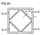
図2Aの実施例では、中央に配置されている発光面21とこれに対応する変換素子31とが別の4つの発光面22−25によって包囲されている。4つの発光面22−25の後方には、各発光面に対応する変換素子32−35が配置されている。つまりこの発光半導体モジュールは、それぞれ対応する変換素子を有する5つの発光領域を含む。各発光面から白色光が放射され、それぞれの発光面の混合光は色座標および/または色温度および/または輝度の点で異なっていてよい。
In the embodiment of FIG. 2A, the
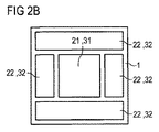
図2Bの実施例では、変換素子31を有する発光面21が、変換素子32を有する別の発光面22によって包囲されている。
In the embodiment of FIG. 2B, the
図2Cの実施例では、発光半導体モジュールの発光ダイオードチップ1はそれぞれ対応する変換素子を有する3つの異なる発光面21−23を含む。
In the embodiment of FIG. 2C, the light emitting
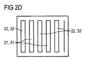
図2Dの実施例では、発光半導体モジュールの発光ダイオードチップ1は、それぞれ条片状に形成された変換素子31,32を備えた2つの発光面21,22を有する。この場合、個々の条片は相互に並列に延在しており、交互に配置されている。発光面21,22から白色混合光が放射され、異なる発光面の混合光は、色座標および/または色温度および/または輝度の点で異なっていてよい。条片状の配置により、放射される光の特に良好な混合が達成される。
In the embodiment of FIG. 2D, the light-emitting
全体として、本発明の発光半導体モジュールの発光ダイオードチップ1は、発光領域、すなわち、発光面およびこれに対応する変換素子に関して、きわめてフレキシブルに構成することができる。複数の異なる発光面を比較的小さな空間に収容することができ、これにより、ほかの光学素子を設けなくても、個々の発光面からの混合光を重畳して放射される全体光につき、離れた箇所において均一な色印象を形成することができる。
As a whole, the light-emitting
図3の概略的な断面図に関連して、本発明の発光半導体モジュールの別の実施例、すなわち、発光ダイオードチップ1の発光領域2a,2bを接続するための導体路65が発光面21,22の下方に配置されている実施例を詳細に説明する。
In connection with the schematic cross-sectional view of FIG. 3, another embodiment of the light-emitting semiconductor module of the present invention, that is, a
発光ダイオードチップ1は、この実施例では、2つの発光領域2a,2bを含む。発光領域2a,2bは電気的絶縁性の分離層61によって電気的に相互に分離されている。
In this embodiment, the light emitting
コンタクト位置5aは、導体路65に導電接続されており、かつ、発光領域2aの発光面21の下方に延在している。コンタクト位置5bは、導体路65に導電接続されており、かつ、発光領域2bの発光面22の下方に延在している。
The
電流は例えば電流拡大層62を介して導体路65から発光領域2a,2bの活性領域64へ印加される。発光面21,22は例えば電磁放射の出射の確率を高める粗面化部63を有することができる。
The current is applied from the
また、各発光領域は、電磁放射を発光面21,22のほうへ反射させるための鏡68を含んでいてもよい。
Each light emitting area may also include a
発光ダイオードチップ1はさらに、接合材料66によって当該の発光ダイオードチップ1の別の領域に接合された支持体67を含む。当該の支持体67は電気的絶縁性を有するように形成してもよい。
The light emitting
導体路が発光面の下方を延在する同様のコンタクト形成のスキーマは、例えば文献DE102007022947A1に詳細に説明されているので、ここではこれ以上立ち入らない。 A similar contact formation scheme in which the conductor track extends below the light emitting surface is described in detail, for example, in document DE102007022947A1, so it will not go further here.
電気抵抗素子4は発光面21,22の下方に配置されている。電気抵抗素子4は発光ダイオードチップ1と支持体67とのあいだに配置されている。電気抵抗素子4は、発光ダイオードチップ1内に集積されており、発光ダイオードチップ1の外表面、すなわち、発光ダイオードチップ1の下側の第2の主表面1bに配置されている。電気抵抗素子4は金属層として構成されており、格子状に配置された複数の導電性セクション41を有する(図1Aを参照)。
The
これに代えて、電気抵抗素子4は発光ダイオードチップ1の下方で支持体67内に集積されてもよい。いずれにしても、電気抵抗素子4は発光ダイオードチップ1によってカバーされ、発光ダイオードチップ1の発光面が縮小されることはない。よって、電気抵抗素子4は発光ダイオードチップ1の発光面21,22の下方に配置されることになるのである。
Alternatively, the
本願は、独国出願第102009037186.9号の優先権を主張する。当該の出願の内容は引用により本発明に含まれるものとする。 The present application claims the priority of German application No. 102009037186.9. The contents of this application are hereby incorporated by reference.
本発明は上述した実施例に限定されない。本発明の新規な種々の特徴は、特許請求の範囲あるいは実施例に特に明示的なことわりがなくても、単独で、または、任意に組み合わせて、本発明の対象となりうる。 The present invention is not limited to the embodiments described above. Various novel features of the present invention can be the subject of the present invention, either alone or in any combination, without any particular remarks in the claims or examples.
Claims (15)
発光半導体モジュールであって、
前記発光ダイオードチップは、相互に独立に動作可能な少なくとも2つの発光領域(2a,2b)と、それぞれ異なって構成された少なくとも2つの変換素子(31,32)とを有しており、
各発光領域(2a,2b)は、前記発光ダイオードチップの動作中に1次電磁放射を形成するために設けられており、かつ、該1次電磁放射の少なくとも一部を前記発光ダイオードチップ(1)から出力するための発光面(21,22)を1つずつ有しており、
前記各変換素子(31,32)は、前記1次電磁放射の少なくとも一部を吸収して2次電磁放射を再放出するために設けられており、かつ、それぞれ各発光面の後方に配置されており、
前記電気抵抗素子(4)は、前記少なくとも2つの発光領域(2a,2b)のうち少なくとも1つに対して直列または並列に接続されている
ことを特徴とする発光半導体モジュール。 A light emitting semiconductor module including a light emitting diode chip (1) and an electric resistance element (4),
The light emitting diode chip has at least two light emitting regions (2a, 2b) that can operate independently from each other, and at least two conversion elements (31, 32) configured differently,
Each light emitting region (2a, 2b) is provided to form primary electromagnetic radiation during operation of the light emitting diode chip, and at least part of the primary electromagnetic radiation is transferred to the light emitting diode chip (1 ) From each of the light emitting surfaces (21, 22) for output from
Each of the conversion elements (31, 32) is provided to absorb at least a part of the primary electromagnetic radiation and re-emit the secondary electromagnetic radiation, and is disposed behind each light emitting surface. And
The light emitting semiconductor module, wherein the electric resistance element (4) is connected in series or in parallel to at least one of the at least two light emitting regions (2a, 2b).
Applications Claiming Priority (3)
| Application Number | Priority Date | Filing Date | Title |
|---|---|---|---|
| DE102009037186A DE102009037186A1 (en) | 2009-08-12 | 2009-08-12 | Radiation-emitting semiconductor component |
| DE102009037186.9 | 2009-08-12 | ||
| PCT/EP2010/061446 WO2011018411A1 (en) | 2009-08-12 | 2010-08-05 | Radiation-emitting semiconductor component |
Publications (2)
| Publication Number | Publication Date |
|---|---|
| JP2013502062A true JP2013502062A (en) | 2013-01-17 |
| JP2013502062A5 JP2013502062A5 (en) | 2013-07-04 |
Family
ID=43037643
Family Applications (1)
| Application Number | Title | Priority Date | Filing Date |
|---|---|---|---|
| JP2012524205A Withdrawn JP2013502062A (en) | 2009-08-12 | 2010-08-05 | Light emitting semiconductor module |
Country Status (7)
| Country | Link |
|---|---|
| US (1) | US9012926B2 (en) |
| EP (1) | EP2465139A1 (en) |
| JP (1) | JP2013502062A (en) |
| KR (1) | KR20120040741A (en) |
| CN (1) | CN102473717A (en) |
| DE (1) | DE102009037186A1 (en) |
| WO (1) | WO2011018411A1 (en) |
Cited By (3)
| Publication number | Priority date | Publication date | Assignee | Title |
|---|---|---|---|---|
| JP2015201614A (en) * | 2014-01-29 | 2015-11-12 | シャープ株式会社 | light-emitting device |
| JP2016054328A (en) * | 2014-01-29 | 2016-04-14 | シャープ株式会社 | Light-emitting device |
| US10342091B2 (en) | 2015-03-13 | 2019-07-02 | Sharp Kabushiki Kaisha | Light-emitting device |
Families Citing this family (25)
| Publication number | Priority date | Publication date | Assignee | Title |
|---|---|---|---|---|
| DE102009047788A1 (en) * | 2009-09-30 | 2011-03-31 | Osram Opto Semiconductors Gmbh | Lighting device for a camera and method for operating the same |
| DE102011015821B4 (en) * | 2011-04-01 | 2023-04-20 | OSRAM Opto Semiconductors Gesellschaft mit beschränkter Haftung | Optoelectronic semiconductor chip |
| US8492182B2 (en) | 2011-04-29 | 2013-07-23 | Osram Opto Semiconductors Gmbh | Method for the producing of a light-emitting semiconductor chip, method for the production of a conversion die and light-emitting semiconductor chip |
| US20220158058A1 (en) * | 2011-06-24 | 2022-05-19 | Creeled, Inc. | Multi-segment monolithic led chip |
| US9299742B2 (en) * | 2011-08-15 | 2016-03-29 | Micron Technology, Inc. | High-voltage solid-state transducers and associated systems and methods |
| DE102012101393A1 (en) * | 2012-02-21 | 2013-08-22 | Osram Opto Semiconductors Gmbh | Method for producing an optoelectronic semiconductor component and optoelectronic semiconductor component |
| DE102012202928A1 (en) * | 2012-02-27 | 2013-08-29 | Osram Gmbh | LIGHT SOURCE WITH LED CHIP AND FLUORESCENT LAYER |
| DE102012202927B4 (en) | 2012-02-27 | 2021-06-10 | Osram Gmbh | LIGHT SOURCE WITH LED CHIP AND LUMINOUS LAYER |
| DE102012101892B4 (en) | 2012-03-06 | 2021-05-12 | OSRAM Opto Semiconductors Gesellschaft mit beschränkter Haftung | Wavelength conversion element, light-emitting semiconductor component and display device therewith as well as method for producing a wavelength conversion element |
| DE102012102301B4 (en) | 2012-03-19 | 2021-06-17 | OSRAM Opto Semiconductors Gesellschaft mit beschränkter Haftung | Optoelectronic semiconductor chip and headlight with such a semiconductor chip |
| DE102012112149A1 (en) | 2012-12-12 | 2014-06-26 | Osram Opto Semiconductors Gmbh | Optoelectronic semiconductor component and method for producing an optoelectronic semiconductor component |
| DE102012112530A1 (en) * | 2012-12-18 | 2014-06-18 | Osram Opto Semiconductors Gmbh | Method for producing optoelectronic semiconductor chips and optoelectronic semiconductor chip |
| JP6328227B2 (en) * | 2014-03-20 | 2018-05-23 | 東芝マテリアル株式会社 | Light emitting device and LED bulb |
| TWI568026B (en) * | 2014-11-04 | 2017-01-21 | 錼創科技股份有限公司 | Light-emitting device |
| DE102015103055A1 (en) * | 2014-12-04 | 2016-06-09 | Osram Opto Semiconductors Gmbh | Optoelectronic semiconductor component and method for producing an optoelectronic semiconductor component |
| KR20170135585A (en) * | 2016-05-31 | 2017-12-08 | 엘지디스플레이 주식회사 | Organic Light Emitting Display device having a bank insulating layer |
| DE102016122237A1 (en) * | 2016-11-18 | 2018-05-24 | Osram Opto Semiconductors Gmbh | Multipixel LED device and method of operating a multi-pixel LED device |
| DE102016224090B4 (en) * | 2016-12-05 | 2024-03-28 | OSRAM Opto Semiconductors Gesellschaft mit beschränkter Haftung | Optoelectronic component, module with at least two optoelectronic components and method for producing an optoelectronic component |
| DE102017106776A1 (en) | 2017-01-30 | 2018-08-02 | Osram Opto Semiconductors Gmbh | Semiconductor device with semiconductor chip |
| KR102563894B1 (en) * | 2017-02-08 | 2023-08-10 | 서울반도체 주식회사 | Light emitting diode and light emitting module comprising the same |
| CN110707189B (en) * | 2017-02-08 | 2023-09-01 | 首尔半导体株式会社 | Light emitting module |
| JPWO2019009033A1 (en) * | 2017-07-03 | 2020-03-19 | シャープ株式会社 | Light source device and light emitting device |
| DE102018111021A1 (en) * | 2017-12-14 | 2019-06-19 | Osram Opto Semiconductors Gmbh | Light-emitting semi-conductor component and method for producing a light-emitting semiconductor component |
| US11054112B2 (en) * | 2017-12-22 | 2021-07-06 | Lumileds Llc | Ceramic phosphor with lateral light barriers |
| EP3614437B1 (en) * | 2018-08-22 | 2021-05-05 | Lumileds LLC | Semiconductor die |
Family Cites Families (11)
| Publication number | Priority date | Publication date | Assignee | Title |
|---|---|---|---|---|
| TW383508B (en) | 1996-07-29 | 2000-03-01 | Nichia Kagaku Kogyo Kk | Light emitting device and display |
| JPH10261818A (en) * | 1997-03-19 | 1998-09-29 | Fujitsu Ltd | Light-emitting semiconductor device |
| JP2001111109A (en) | 1999-10-07 | 2001-04-20 | Sharp Corp | Gallium nitride compound semiconductor light emitting device |
| DE602005022067D1 (en) | 2004-06-04 | 2010-08-12 | Philips Intellectual Property | ELECTROLUMINESCENCE STRUCTURE AND LED WITH AN EL STRUCTURE |
| CN101268554A (en) * | 2005-09-19 | 2008-09-17 | 皇家飞利浦电子股份有限公司 | Variable color light emitting device and method for controlling the same |
| JP2007294878A (en) | 2006-03-31 | 2007-11-08 | Fujifilm Corp | Semiconductor layer, depositing method, semiconductor light emitting device and semiconductor luminescent device |
| JP2007287842A (en) * | 2006-04-14 | 2007-11-01 | Ricoh Co Ltd | Semiconductor device |
| US7714348B2 (en) * | 2006-10-06 | 2010-05-11 | Ac-Led Lighting, L.L.C. | AC/DC light emitting diodes with integrated protection mechanism |
| DE102007022947B4 (en) | 2007-04-26 | 2022-05-05 | OSRAM Opto Semiconductors Gesellschaft mit beschränkter Haftung | Optoelectronic semiconductor body and method for producing such |
| EP2089915B1 (en) * | 2007-08-03 | 2018-08-01 | Panasonic Intellectual Property Management Co., Ltd. | Wavelength-converted light-emitting device with uniform emission |
| US7968902B2 (en) * | 2008-03-31 | 2011-06-28 | Bridgelux, Inc. | Light emitting devices with constant forward voltage |
-
2009
- 2009-08-12 DE DE102009037186A patent/DE102009037186A1/en not_active Withdrawn
-
2010
- 2010-08-05 JP JP2012524205A patent/JP2013502062A/en not_active Withdrawn
- 2010-08-05 WO PCT/EP2010/061446 patent/WO2011018411A1/en active Application Filing
- 2010-08-05 EP EP10740230A patent/EP2465139A1/en not_active Withdrawn
- 2010-08-05 KR KR1020127006427A patent/KR20120040741A/en not_active Application Discontinuation
- 2010-08-05 CN CN2010800356637A patent/CN102473717A/en active Pending
- 2010-08-05 US US13/389,661 patent/US9012926B2/en not_active Expired - Fee Related
Cited By (3)
| Publication number | Priority date | Publication date | Assignee | Title |
|---|---|---|---|---|
| JP2015201614A (en) * | 2014-01-29 | 2015-11-12 | シャープ株式会社 | light-emitting device |
| JP2016054328A (en) * | 2014-01-29 | 2016-04-14 | シャープ株式会社 | Light-emitting device |
| US10342091B2 (en) | 2015-03-13 | 2019-07-02 | Sharp Kabushiki Kaisha | Light-emitting device |
Also Published As
| Publication number | Publication date |
|---|---|
| WO2011018411A1 (en) | 2011-02-17 |
| KR20120040741A (en) | 2012-04-27 |
| US9012926B2 (en) | 2015-04-21 |
| CN102473717A (en) | 2012-05-23 |
| US20120193657A1 (en) | 2012-08-02 |
| DE102009037186A1 (en) | 2011-02-17 |
| EP2465139A1 (en) | 2012-06-20 |
Similar Documents
| Publication | Publication Date | Title |
|---|---|---|
| JP2013502062A (en) | Light emitting semiconductor module | |
| TWI446593B (en) | Method for manufacturing an optoelectronic semiconductor component and said optoelectronic semiconductor component | |
| JP5431329B2 (en) | Semiconductor component and method for manufacturing semiconductor component | |
| TWI515927B (en) | Semiconductor light emitting device and method for manufacturing same | |
| US7439549B2 (en) | LED module | |
| US6476410B2 (en) | Backside light emitting chip type light emitting element and insulating substrate therefor | |
| KR101255121B1 (en) | Lighting emitting diode package and Method for manufacturing the same | |
| JP2013502062A5 (en) | ||
| JP5372009B2 (en) | Optoelectronic component and manufacturing method thereof | |
| JP2007067326A (en) | Light emitting diode and method of manufacturing same | |
| JPWO2005106978A1 (en) | Light emitting device and manufacturing method thereof | |
| TWI438888B (en) | Optoelectronic module with a carrier substrate and a plurality of radiation-emitting semiconductor devices and its manufacturing method | |
| TWI431806B (en) | Optoelectronic component | |
| JP2010130008A (en) | Side view type led package structure, and manufacturing method and application thereof | |
| JP2006173326A (en) | Optical source apparatus | |
| US20090154176A1 (en) | Electronic component and method for manufacturing same | |
| WO2012042333A1 (en) | Led module | |
| KR20130062985A (en) | Radiation-emitting component and method for producing a radiation-emitting component | |
| JP2009177095A (en) | Light-emitting device | |
| KR101900987B1 (en) | Mixed light source | |
| JP5178619B2 (en) | Semiconductor device substrate and semiconductor device | |
| JP2009206186A (en) | Light emitting device | |
| WO2022004410A1 (en) | Method for manufacturing base member, method for manufacturing light-emitting device, base member, and light-emitting device | |
| US20140183565A1 (en) | Light-Emitting Module Board and Manufacturing Method of the Light-Emitting Module Board | |
| JP5116551B2 (en) | Light emitting device |
Legal Events
| Date | Code | Title | Description |
|---|---|---|---|
| A521 | Written amendment |
Free format text: JAPANESE INTERMEDIATE CODE: A523 Effective date: 20130514 |
|
| A621 | Written request for application examination |
Free format text: JAPANESE INTERMEDIATE CODE: A621 Effective date: 20130514 |
|
| A977 | Report on retrieval |
Free format text: JAPANESE INTERMEDIATE CODE: A971007 Effective date: 20140122 |
|
| A761 | Written withdrawal of application |
Free format text: JAPANESE INTERMEDIATE CODE: A761 Effective date: 20140131 |