JP2013500524A - IOMMU with two-level address translation for I / O and computational load reduction devices in peripheral interconnects - Google Patents
IOMMU with two-level address translation for I / O and computational load reduction devices in peripheral interconnects Download PDFInfo
- Publication number
- JP2013500524A JP2013500524A JP2012521868A JP2012521868A JP2013500524A JP 2013500524 A JP2013500524 A JP 2013500524A JP 2012521868 A JP2012521868 A JP 2012521868A JP 2012521868 A JP2012521868 A JP 2012521868A JP 2013500524 A JP2013500524 A JP 2013500524A
- Authority
- JP
- Japan
- Prior art keywords
- guest
- translation
- request
- control logic
- address
- Prior art date
- Legal status (The legal status is an assumption and is not a legal conclusion. Google has not performed a legal analysis and makes no representation as to the accuracy of the status listed.)
- Granted
Links
- 238000013519 translation Methods 0.000 title claims abstract description 154
- 230000002093 peripheral effect Effects 0.000 title claims description 16
- 230000015654 memory Effects 0.000 claims abstract description 178
- 230000014616 translation Effects 0.000 claims abstract description 153
- 238000012545 processing Methods 0.000 claims abstract description 20
- 238000000034 method Methods 0.000 claims description 24
- 230000008569 process Effects 0.000 claims description 17
- 230000006658 host protein synthesis Effects 0.000 claims description 13
- 230000004044 response Effects 0.000 claims description 10
- 238000004519 manufacturing process Methods 0.000 claims 1
- 238000010586 diagram Methods 0.000 description 16
- 238000012986 modification Methods 0.000 description 9
- 230000004048 modification Effects 0.000 description 9
- 230000006870 function Effects 0.000 description 7
- 230000007246 mechanism Effects 0.000 description 5
- 239000000872 buffer Substances 0.000 description 4
- 230000008859 change Effects 0.000 description 4
- 238000013507 mapping Methods 0.000 description 4
- 230000001427 coherent effect Effects 0.000 description 2
- 238000004891 communication Methods 0.000 description 2
- 238000002955 isolation Methods 0.000 description 2
- 238000013459 approach Methods 0.000 description 1
- 238000013480 data collection Methods 0.000 description 1
- 230000003287 optical effect Effects 0.000 description 1
- 230000000750 progressive effect Effects 0.000 description 1
- 239000004065 semiconductor Substances 0.000 description 1
- 239000007787 solid Substances 0.000 description 1
- 230000003068 static effect Effects 0.000 description 1
- 230000001360 synchronised effect Effects 0.000 description 1
- 238000011144 upstream manufacturing Methods 0.000 description 1
Images


Classifications
-
- G—PHYSICS
- G06—COMPUTING; CALCULATING OR COUNTING
- G06F—ELECTRIC DIGITAL DATA PROCESSING
- G06F12/00—Accessing, addressing or allocating within memory systems or architectures
- G06F12/02—Addressing or allocation; Relocation
- G06F12/08—Addressing or allocation; Relocation in hierarchically structured memory systems, e.g. virtual memory systems
- G06F12/10—Address translation
- G06F12/1081—Address translation for peripheral access to main memory, e.g. direct memory access [DMA]
-
- G—PHYSICS
- G06—COMPUTING; CALCULATING OR COUNTING
- G06F—ELECTRIC DIGITAL DATA PROCESSING
- G06F12/00—Accessing, addressing or allocating within memory systems or architectures
- G06F12/02—Addressing or allocation; Relocation
- G06F12/08—Addressing or allocation; Relocation in hierarchically structured memory systems, e.g. virtual memory systems
- G06F12/10—Address translation
- G06F12/1009—Address translation using page tables, e.g. page table structures
-
- G—PHYSICS
- G06—COMPUTING; CALCULATING OR COUNTING
- G06F—ELECTRIC DIGITAL DATA PROCESSING
- G06F12/00—Accessing, addressing or allocating within memory systems or architectures
- G06F12/02—Addressing or allocation; Relocation
- G06F12/0223—User address space allocation, e.g. contiguous or non contiguous base addressing
- G06F12/0292—User address space allocation, e.g. contiguous or non contiguous base addressing using tables or multilevel address translation means
-
- G—PHYSICS
- G06—COMPUTING; CALCULATING OR COUNTING
- G06F—ELECTRIC DIGITAL DATA PROCESSING
- G06F12/00—Accessing, addressing or allocating within memory systems or architectures
- G06F12/02—Addressing or allocation; Relocation
- G06F12/06—Addressing a physical block of locations, e.g. base addressing, module addressing, memory dedication
- G06F12/0615—Address space extension
- G06F12/063—Address space extension for I/O modules, e.g. memory mapped I/O
-
- G—PHYSICS
- G06—COMPUTING; CALCULATING OR COUNTING
- G06F—ELECTRIC DIGITAL DATA PROCESSING
- G06F12/00—Accessing, addressing or allocating within memory systems or architectures
- G06F12/02—Addressing or allocation; Relocation
- G06F12/08—Addressing or allocation; Relocation in hierarchically structured memory systems, e.g. virtual memory systems
- G06F12/0802—Addressing of a memory level in which the access to the desired data or data block requires associative addressing means, e.g. caches
- G06F12/0866—Addressing of a memory level in which the access to the desired data or data block requires associative addressing means, e.g. caches for peripheral storage systems, e.g. disk cache
- G06F12/0868—Data transfer between cache memory and other subsystems, e.g. storage devices or host systems
-
- G—PHYSICS
- G06—COMPUTING; CALCULATING OR COUNTING
- G06F—ELECTRIC DIGITAL DATA PROCESSING
- G06F12/00—Accessing, addressing or allocating within memory systems or architectures
- G06F12/02—Addressing or allocation; Relocation
- G06F12/08—Addressing or allocation; Relocation in hierarchically structured memory systems, e.g. virtual memory systems
- G06F12/0802—Addressing of a memory level in which the access to the desired data or data block requires associative addressing means, e.g. caches
- G06F12/0877—Cache access modes
- G06F12/0882—Page mode
-
- G—PHYSICS
- G06—COMPUTING; CALCULATING OR COUNTING
- G06F—ELECTRIC DIGITAL DATA PROCESSING
- G06F12/00—Accessing, addressing or allocating within memory systems or architectures
- G06F12/02—Addressing or allocation; Relocation
- G06F12/08—Addressing or allocation; Relocation in hierarchically structured memory systems, e.g. virtual memory systems
- G06F12/0802—Addressing of a memory level in which the access to the desired data or data block requires associative addressing means, e.g. caches
- G06F12/0893—Caches characterised by their organisation or structure
- G06F12/0897—Caches characterised by their organisation or structure with two or more cache hierarchy levels
-
- G—PHYSICS
- G06—COMPUTING; CALCULATING OR COUNTING
- G06F—ELECTRIC DIGITAL DATA PROCESSING
- G06F3/00—Input arrangements for transferring data to be processed into a form capable of being handled by the computer; Output arrangements for transferring data from processing unit to output unit, e.g. interface arrangements
- G06F3/06—Digital input from, or digital output to, record carriers, e.g. RAID, emulated record carriers or networked record carriers
- G06F3/0601—Interfaces specially adapted for storage systems
- G06F3/0628—Interfaces specially adapted for storage systems making use of a particular technique
- G06F3/0629—Configuration or reconfiguration of storage systems
- G06F3/0631—Configuration or reconfiguration of storage systems by allocating resources to storage systems
-
- G—PHYSICS
- G06—COMPUTING; CALCULATING OR COUNTING
- G06F—ELECTRIC DIGITAL DATA PROCESSING
- G06F3/00—Input arrangements for transferring data to be processed into a form capable of being handled by the computer; Output arrangements for transferring data from processing unit to output unit, e.g. interface arrangements
- G06F3/06—Digital input from, or digital output to, record carriers, e.g. RAID, emulated record carriers or networked record carriers
- G06F3/0601—Interfaces specially adapted for storage systems
- G06F3/0628—Interfaces specially adapted for storage systems making use of a particular technique
- G06F3/0638—Organizing or formatting or addressing of data
- G06F3/064—Management of blocks
-
- G—PHYSICS
- G06—COMPUTING; CALCULATING OR COUNTING
- G06F—ELECTRIC DIGITAL DATA PROCESSING
- G06F3/00—Input arrangements for transferring data to be processed into a form capable of being handled by the computer; Output arrangements for transferring data from processing unit to output unit, e.g. interface arrangements
- G06F3/06—Digital input from, or digital output to, record carriers, e.g. RAID, emulated record carriers or networked record carriers
- G06F3/0601—Interfaces specially adapted for storage systems
- G06F3/0668—Interfaces specially adapted for storage systems adopting a particular infrastructure
- G06F3/067—Distributed or networked storage systems, e.g. storage area networks [SAN], network attached storage [NAS]
-
- G—PHYSICS
- G06—COMPUTING; CALCULATING OR COUNTING
- G06F—ELECTRIC DIGITAL DATA PROCESSING
- G06F3/00—Input arrangements for transferring data to be processed into a form capable of being handled by the computer; Output arrangements for transferring data from processing unit to output unit, e.g. interface arrangements
- G06F3/06—Digital input from, or digital output to, record carriers, e.g. RAID, emulated record carriers or networked record carriers
- G06F3/0601—Interfaces specially adapted for storage systems
- G06F3/0668—Interfaces specially adapted for storage systems adopting a particular infrastructure
- G06F3/0671—In-line storage system
- G06F3/0683—Plurality of storage devices
Landscapes
- Engineering & Computer Science (AREA)
- Theoretical Computer Science (AREA)
- Physics & Mathematics (AREA)
- General Engineering & Computer Science (AREA)
- General Physics & Mathematics (AREA)
- Memory System Of A Hierarchy Structure (AREA)
Abstract
【解決手段】
コンピュータシステムのシステムメモリへのI/Oデバイスによる要求を制御するためのIOMMUは、制御論理及びキャッシュメモリを含む。制御論理は、I/Oデバイスからの要求において受信されるアドレスをトランスレートしてよい。要求が処理アドレス空間識別子(PASID)プレフィックスを伴うトランザクション層プロトコル(TLP)パケットを含む場合には、制御論理は2レベルのゲストトランスレーションを実行してよい。従って、制御論理は、ゲストページテーブルのセットにアクセスして、要求において受信されるアドレスをトランスレートしてよい。最後のゲストページテーブル内のポインタは、入れ子にされたページテーブルのセット内の第1のテーブルを指し示す。制御論理は、入れ子にされたページテーブルのセットにアクセスしてシステムメモリ内の物理ページに対応するシステム物理アドレス(SPA)を得るために、最後のゲストページテーブル内のポインタを用いてよい。キャッシュメモリは完了したトランスレーションを記憶する。
【選択図】図5[Solution]
An IOMMU for controlling requests by I / O devices to the system memory of a computer system includes control logic and cache memory. The control logic may translate the address received in the request from the I / O device. If the request includes a transaction layer protocol (TLP) packet with a processing address space identifier (PASID) prefix, the control logic may perform two levels of guest translation. Thus, the control logic may access the set of guest page tables and translate the address received in the request. The pointer in the last guest page table points to the first table in the set of nested page tables. The control logic may use the pointer in the last guest page table to access a nested set of page tables to obtain the system physical address (SPA) corresponding to the physical page in system memory. The cache memory stores completed translations.
[Selection] Figure 5
Description
本発明はコンピュータシステムの分野に関し、より特定的には入力/出力(I/O)デバイスのためのメモリ管理ユニットに関する。 The present invention relates to the field of computer systems, and more particularly to memory management units for input / output (I / O) devices.
現代社会では、パーソナルコンピュータ(PC)、ワークステーション、サーバ、種々のパーソナルデジタルアシスタント(PDA)デバイス等を含む様々な種類のコンピュータシステムが遍在している。全てではないにしろこれらコンピュータシステムの多くは、プロセッサがメモリにアクセスするために実装されるメモリ管理機能を有している。一般に、メモリ管理機能は、各処理によって用いられる仮想アドレス空間から実際のシステムメモリに広がる物理アドレス空間へアドレスをトランスレートすることや、種々のメモリ保護(例えばリードオンリ、リード/ライト、特権レベル要求、等)を含んできた。メモリ管理機能は、各処理によって用いられるメモリを他の処理による権限のないアクセスから保護すること、物理メモリシステムが大きくない場合であっても大きな仮想空間が処理によって用いられることを可能にすること、利用可能な物理メモリへ仮想アドレスを処理に関与することなしに再配置すること等のような種々の用途を有している。 In modern society, various types of computer systems are ubiquitous including personal computers (PCs), workstations, servers, various personal digital assistant (PDA) devices, and the like. Many, if not all, of these computer systems have memory management functions implemented for the processor to access the memory. In general, the memory management function translates an address from a virtual address space used by each process to a physical address space extending to actual system memory, and performs various types of memory protection (for example, read only, read / write, privilege level request, Etc.). The memory management function protects the memory used by each process from unauthorized access by other processes, and allows a large virtual space to be used by the process even when the physical memory system is not large Have various uses such as relocating virtual addresses to available physical memory without being involved in processing.
プロセッサアドレスはしばしばトランスレートされるが、コンピュータシステムにおける入力/出力(I/O)デバイスによって用いられるアドレスは、一般にはトランスレートされない。即ち、I/Oデバイスはメモリにアクセスするために物理アドレスを用いる。多くのPCのような単一オペレーティングシステム(OS)コンピュータシステムにおいては、他の処理(アプリケーション及びOSサービス)によるI/OデバイスへのアクセスをOSが制御する。従ってOSは、任意の所与の時点で所与のデバイスへのアクセスをどの処理が有するかを制御することができ、またそのデバイスによってアクセスされるアドレスを少なくとも多少は制御することができる。しかし、そのようなメカニズムは、仮想マシンモニタ上で動作している多重ゲストOSを有するであろう仮想マシンシステムにおいては、より複雑で且つ扱いにくいものになる。加えて、不正デバイス(又は悪意のあるソフトウエアエージェントによってプログラムされたデバイス)が妨げられずにメモリにアクセス可能であることから、デバイスが物理アドレスを使用することは、システムの全体的なセキュリティを低下させる。 While processor addresses are often translated, addresses used by input / output (I / O) devices in computer systems are generally not translated. That is, the I / O device uses a physical address to access the memory. In a single operating system (OS) computer system such as many PCs, the OS controls access to I / O devices by other processes (applications and OS services). Thus, the OS can control which processes have access to a given device at any given time, and can control at least some of the addresses accessed by that device. However, such a mechanism becomes more complex and cumbersome in a virtual machine system that will have multiple guest OSes running on a virtual machine monitor. In addition, the use of a physical address by the device reduces the overall security of the system, since unauthorized devices (or devices programmed by malicious software agents) can access the memory unimpeded. Reduce.
仮想化されたシステムにおいては、多くのアプリケーションが仮想メモリ内で動作するであろう一方で、I/Oデバイスは物理メモリにアクセスする。幾つかのシステムでは、仮想マシンマネージャが、I/Oデバイスによって用いられることになるアドレスをインターセプトすると共にトランスレートするかもしれない。しかし、この手法は、面倒であると共に命令集約的であろうから、システム性能を低下させ、あるいは少なくとも計算負荷軽減エンジン(computational offload engine)のようなI/Oデバイスを用いることによって得られる任意の利益を減らしてしまうかもしれない。 In a virtualized system, many applications will run in virtual memory, while I / O devices access physical memory. In some systems, a virtual machine manager may intercept and translate addresses that will be used by I / O devices. However, this approach would be cumbersome and instruction intensive, thus reducing system performance or at least any gain obtained by using an I / O device such as a computational offload engine. May reduce profits.
2レベルのトランスレーションを用いるIOMMUの種々の実施形態が開示される。1つの実施形態においては、コンピュータシステムのシステムメモリへのI/Oデバイスによる要求を制御するためのIOMMUは、制御論理及びキャッシュメモリを含む。制御論理は、I/Oデバイスからの要求において受信されるアドレスをトランスレートするように構成されてよい。要求が処理アドレス空間識別子(PASID)プレフィックスを伴うトランザクション層プロトコル(TLP)パケットを含む場合には、制御論理は2レベルのゲストトランスレーションを実行するように構成される。要求内のPASIDプレフィックスの存在は、受信されたアドレスがゲスト仮想アドレス(GVA)であることを表示する。従って、2レベルのゲストトランスレーションを実行するために、制御論理は、ゲストページテーブルのセットにアクセスして、要求において受信されるアドレスをトランスレートするように構成されされてよい。最後のゲストページテーブル内のポインタは、入れ子にされたページテーブルのセット内の第1のテーブルを指し示す。制御論理は、入れ子にされたページテーブルのセットにアクセスしてシステムメモリ内の物理ページに対応するシステム物理アドレス(SPA)を得るために、最後のゲストページテーブル内のポインタを用いるように構成される。キャッシュメモリは、後続のトランスレーションのために用いられ得る完了したトランスレーションを記憶するように構成されてよい。 Various embodiments of IOMMU using two levels of translation are disclosed. In one embodiment, an IOMMU for controlling requests by an I / O device to system memory of a computer system includes control logic and cache memory. The control logic may be configured to translate the address received in the request from the I / O device. If the request includes a transaction layer protocol (TLP) packet with a processing address space identifier (PASID) prefix, the control logic is configured to perform two levels of guest translation. The presence of the PASID prefix in the request indicates that the received address is a guest virtual address (GVA). Thus, to perform two levels of guest translation, the control logic may be configured to access a set of guest page tables to translate the address received in the request. The pointer in the last guest page table points to the first table in the set of nested page tables. The control logic is configured to use the pointer in the last guest page table to access the nested set of page tables and obtain the system physical address (SPA) corresponding to the physical page in system memory. The The cache memory may be configured to store completed translations that can be used for subsequent translations.
本発明は種々の修正及び代替的形態を許容する一方で、その具体的な実施形態は、例示として図面に示され、またここに詳細に説明されることになる。但し、図面及びそれに対する詳細な説明は、開示される特定の形態に本発明を限定することを意図しているのではなく、むしろ逆に、添付の特許請求の範囲によって画定される本発明の精神及び範囲内に含まれる全ての修正、均等なもの、及び代替を網羅することが意図されている。尚、「〜であってよい、〜であろう、〜ことがある、〜し得る、〜かもしれない(may)」の語は、この出願を通して、必須の意味(即ち、〜しなければならない)の意味ではなく、許容の意味(即ち、〜する可能性がある、〜することができる)で用いられている。 While the invention is susceptible to various modifications and alternative forms, specific embodiments thereof are shown by way of example in the drawings and will herein be described in detail. However, the drawings and detailed description thereof are not intended to limit the invention to the particular forms disclosed, but rather are directed to the invention as defined by the appended claims. It is intended to cover all modifications, equivalents, and alternatives falling within the spirit and scope. It should be noted that the term “may be, will be, may be, may be, may be,” is used throughout this application to mean the essential meaning (ie, ) Is used in an acceptable sense (i.e., may or may be).
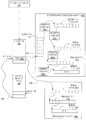
図1を参照すると、コンピュータシステム10の1つの実施形態の単純化された高位レベルのブロック図が示されている。図示される例では、システム10は、1つ以上のプロセッサ12と、1つ以上のトランスレーションルックアサイドバッファ(TLB)16を備えているメモリ管理ユニット(MMU)14と、メモリ制御器(MC)18と、メモリ20と、1つ以上のI/O_TLB(IOTLB)24を備えていてよい1つ以上のI/Oデバイス22と、テーブルウォーカ28、キャッシュ30、制御レジスタ32、及び制御論理34を備えていてよいI/O_MMU(IOMMU)26とを含む。プロセッサ12はMMU14に結合され、MMU14はメモリ制御器18に結合される。I/Oデバイス22はIOMMU26に結合され、IOMMU26はメモリ制御器18に結合される。IOMMU26内においては、テーブルウォーカ28、キャッシュ30、制御レジスタ32、及び制御論理34は互いに結合される。
Referring to FIG. 1, a simplified high level block diagram of one embodiment of a
後で更に説明されるように、IOMMU26はシステム10における仮想化を単純化するための種々の特徴を含んでいてよい。以下の説明は、仮想マシンを管理(基礎となるハードウエア上でのそれらの実行をスケジューリングすること)し、種々のシステム資源へのアクセスを制御する等の仮想マシンモニタ(VMM)を参照することになる。尚、VMMはしばしばハイパーバイザとも称される。図示される実施形態においては、単一又は複数のプロセッサ12が仮想環境でソフトウエアを実行している。従って、3つの仮想マシン100A、100B、及び100C(例えばVMゲスト1〜3)並びにVMM106が図示されている。所与の実施形態における仮想マシンの数は変化してよく、また仮想マシンがユーザによって起動され停止されるのに従って動的に変化してよい。図示される実施形態においては、仮想マシン100Aは、1つ以上のゲストアプリケーション102と、ゲストオペレーティングシステム(OS)104とを含む。OS104は、システム10の物理的なハードウエアよりはむしろ、VMM106によってOS104のために作り出される仮想マシンを制御するので、OS104は「ゲスト」OSと称される。同様にVM100B及び100Cもまた、1つ以上のゲストアプリケーション、及びゲストOSを各々が含む。
As described further below, IOMMU 26 may include various features to simplify virtualization in
一般に仮想マシン内のアプリケーションは、ゲスト仮想アドレス空間、及びこれに伴いゲスト仮想アドレス(GVA)を用いる。各仮想マシン内のゲストOSは、その仮想マシン内でのゲスト「物理」アドレス(GPA)へのGVAのマッピングを管理してよい。ゲストOSがVMMなしに直接システム10ハードウエア上で動作している場合には、ゲストOSによって生成される物理アドレスが、実際にはシステム10内のメモリロケーションのシステム物理アドレス(SPA)になるであろう。しかし、仮想マシン環境においては、GPAからSPAへのマッピングをVMM106が管理してよい。このように、プロセッサ12がメモリ要求を実行する場合には、ゲストOS104がGPA(VMM106によってSPAへと更にマッピングされ得る)へのGVAのマッピングを管理してよい。
In general, an application in a virtual machine uses a guest virtual address space and a guest virtual address (GVA). The guest OS in each virtual machine may manage the mapping of GVA to the guest “physical” address (GPA) in that virtual machine. If the guest OS is operating directly on the
図1に示されるように、I/Oデバイス22からメモリ20へのパスは、少なくとも部分的にはプロセッサ12からメモリ20へのパスからは分離されている。具体的には、I/Oデバイス22からメモリ20へのパスは、MMU14を通過しないが、その代わりにIOMMU26を経由している。従って、MMU14は、I/Oデバイス22から供給されるメモリ要求に対してはメモリ管理を提供しないであろう。一般にメモリ管理は、1つの種類の仮想アドレス(即ちソフトウエアによって用いられるであろうアドレス)から物理アドレス(即ちメモリ制御器によって用いられるであろうアドレス)へのアドレストランスレーションとメモリ保護とからなる。メモリ保護は、なんらかのレベルの精度(例えばページ)に加えて、種々の他の属性、例えば特権レベル要求、キャッシュ能力及びキャッシュ制御(例えばライトスルー又はライトバック)、コヒーレンシ等でメモリに対する読み出し及び/又は書き込みを制御してよい。任意の一連のメモリ保護が種々の実施形態において実装され得る。幾つかの実施形態においては、IOMMU26によって実装されるメモリ保護は、少なくともなんらかの点においてMMU14によって実装されるメモリ保護とは異なることがある。1つの実施形態では、IOMMU26によって実装されるメモリ保護は、IOMMU26及びMMU14によって用いられるトランスレーションデータを記憶しているトランスレーションテーブルが共有され得るように定義されてよい(議論の容易化のために図1では別個に図示されているが)。後で更に説明されるように、トランスレーションテーブル情報を共有する幾つかの実施形態においては、特権が変化する場合のように特定のページが促進された場合には、いまや信頼できないものになっているであろうトランスレーションページテーブルを更新するためにテーブル再ウォークが必要になるであろう。他の実施形態は、要望に応じてIOMMU26とMMU14の間でトランスレーションテーブルを共有しなくてよい。
As shown in FIG. 1, the path from the I /
概してI/Oデバイス22は、メモリ20内のメモリロケーションにアクセスするメモリ読み出し及び書き込み要求のようなメモリ要求を、そして幾つかのケースではトランスレーション要求を発行するように構成されてよい。メモリ要求は、例えば、直接メモリアクセス(DMA)読み出し又は書き込み動作の一部であってよい。DMA動作はプロセッサ12によって実行されているソフトウエアによって開始されてよく、ソフトウエアは、DMA動作を直接的に又は間接的に実行するようにI/Oデバイス22をプログラミングしている。プロセッサ上で実行中のソフトウエアが動作しているアドレス空間に応じて、メモリ20にアクセスするための当該アドレス空間に対応するアドレスがI/Oデバイス22へ提供されてよい。例えば、プロセッサ12上で実行中のゲストアプリケーション(例えばApp102)は、I/Oデバイス22にGVAを提供してよい一方で、プロセッサ12上で実行中のゲストOS(例えばOS104)は、I/Oデバイス22にGPAを提供してよい。いずれの場合においても、I/Oデバイス22がメモリアクセスを要求するときには、ゲストアドレスは、IOMMU26によって、メモリにアクセスするための対応するシステム物理アドレス(SPA)へとトランスレートされるであろうし、そしてシステム物理アドレスがアクセスのためにメモリ制御器18に提供されるであろう。即ちIOMMU26は、I/Oデバイス22によって供給されるメモリ要求を修正して、要求における受信したアドレスをSPAへと変化させて(即ちトランスレートして)よく、そしてメモリ要求は、メモリ制御器18がメモリ20にアクセスするためにメモリ制御器18へと転送されてよい。
In general, I /
種々の実施形態において、IOMMU26は、それがI/Oデバイスから受け取るアドレスの種類に応じて、1レベル若しくは2レベルのトランスレーションを提供し又はトランスレーションを提供しなくてよい。より特定的には、IOMMU26は、1レベルの入れ子にされた(nested)トランスレーション又は2レベルのゲストトランスレーションを実行してよい。つまり、IOMMU26は、GPAからSPAへのトランスレーション(1レベル)及びGVAからSPAへのトランスレーション(2レベル)の両方を提供することができる。このように、ゲストアプリケーションは、メモリアクセスを要求する場合には、上述の通りGVAアドレスを直接I/Oデバイスに供給することができ、それにより従来のVMMインターセプション及びトランスレーションを不要にすることができる。この機能性は、進歩的な計算アーキテクチャ、例えば計算から解放された(compute offload)デバイス、ユーザレベルのI/Oデバイス、及び加速されたI/Oデバイスが、仮想化されたシステムにおいてより途切れなく用いられることを可能にするであろう。尚、1レベル若しくは2レベルのトランスレーション又はトランスレーションなしが説明されているが、他の実施形態においては、追加的なレベルのアドレス空間が用いられ得ることが検討される。そのような実施形態においては、追加のレベルのトランスレーション(即ち多重レベルトランスレーション)は、IOMMU26が追加的なアドレス空間に適合することによって行われてよい。
In various embodiments, the
後で更に詳細に説明されるように、IOMMU26は、それが所与の要求において受信しているアドレスの種類が何であるかを認識するための手段を有していることが必要である。従って、例えばI/OデバイスがIOMMU26にPCIエクスプレス(PCI express)(PCIe)相互接続のような標準的な周辺バスを介して結合されている実施形態においては、トランスレーション層プロトコル(TLP)プレフィックス(prefix)を用いて処理アドレス空間識別子(process address space identifier)(PASID)がIOMMU26へ送られてよい。
As will be explained in more detail later, the
IOMMU26は、メモリのアドレス及びI/Oデバイス22からのトランスレーション要求をトランスレートするために、幾つかのデータ構造、例えばメモリ20内に記憶されているI/Oトランスレーションテーブル36の1つ以上のセットを用いてよい。一般にトランスレーションテーブルは、アドレスを1つの種類から別の種類へとトランスレートするために用いられ得るトランスレーションデータのテーブルであってよい。トランスレーションテーブルは、トランスレーションデータを任意の方法で記憶していてよい。例えば1つの実施形態においては、I/Oトランスレーションテーブル36は、x86及びAMD64(商標)命令セットアーキテクチャにおいて定義されるのと同様のページテーブルを含んでいてよい。トランスレーションレベルに応じて、ゲスト仮想アドレスビットの種々のサブセット又はゲスト物理アドレスがテーブルのレベルを索引付けるために用いられてよく、そして各レベルは、トランスレーションの終点(即ちトランスレーションに対する実際のページ番号を記憶している)又は別のテーブルへの点(別のセットのアドレスビットによって索引付けられている)のいずれかであってよい。ページはトランスレーションの単位であってよい(即ち仮想ページ内の各アドレスは同じ物理ページへトランスレートする)。ページは4キロバイトからメガバイト又はギガバイトまで変化するサイズを有していてよい。
The
また、I/Oトランスレーションテーブル36は、I/Oデバイスをページテーブルのセットにマッピングする(例えばデバイス識別子によって)デバイステーブル(図3に図示)を含んでいてよい。デバイス識別子(ID)は種々の方法において定義されてよく、またデバイスが接続される周辺相互接続に依存するであろう。例えば、周辺コンポーネント相互接続(Peripheral Component Interconnect)(PCI)デバイスは、バス番号、デバイス番号、及び機能番号(BDF)からデバイスIDを形成してよい。ハイパートランスポート(HyperTransport)(HT)デバイスは、バス番号及びユニットIDを用いてデバイスIDを形成してよい。後で更に説明されるように、デバイステーブルはデバイスIDによって索引付けられる複数のエントリを含んでいてよく、そして各エントリは、対応するデバイスIDを有するデバイスによって用いられるページテーブルのセットへのポインタを含んでいてよい。また、I/Oデバイスが処理に直接割り当てられており又はユーザ処理と同じアドレス空間において計算を実行する可能性がある場合には、メモリ隔離保護を強化するために、処理アドレス空間が識別されると共にIOMMU26へ提供されてよい。幾つかの実施形態においては、デバイステーブルは、デバイスのインターラプトを再マッピングするために、インターラプト再マッピングテーブル(図3に図示)へのポインタを更に含んでいてよい。このように、概して、GVA又はGPAからSPAへのトランスレーションは、1つ以上のトランスレーションテーブルにおける1つ以上のエントリ内に記憶されてよく、そして幾つかのエントリは、他のトランスレーションと共有されてよい。エントリからエントリへとテーブルを横断すること又は「ウォーキングすること」が、仮想アドレスに対するトランスレーションを識別することの一部であってよい。1つの実施形態においては、トランスレーションテーブル36は、上述のインターラプト再マッピングテーブルを含んでいてよい。
The I / O translation table 36 may also include a device table (shown in FIG. 3) that maps I / O devices to a set of page tables (eg, by device identifier). A device identifier (ID) may be defined in various ways and will depend on the peripheral interconnect to which the device is connected. For example, a Peripheral Component Interconnect (PCI) device may form a device ID from a bus number, device number, and function number (BDF). A HyperTransport (HT) device may form a device ID using a bus number and a unit ID. As described further below, the device table may contain multiple entries indexed by device ID, and each entry contains a pointer to a set of page tables used by the device having the corresponding device ID. May contain. Also, if the I / O device is directly assigned to a process or may perform calculations in the same address space as the user process, the process address space is identified to enhance memory isolation protection. Together with the
具体的には、図1に示されるIOMMU26は、所与のメモリ要求に対するトランスレーションのためにI/Oトランスレーションテーブル36を検索するテーブルウォーカ28を含んでいてよい。テーブルウォーカ28は、トランスレーションテーブル36からトランスレーションデータを読み出すために、メモリ要求、例えば読み出しメモリ要求を生成してよい。トランスレーションテーブル読み出しは、図1において点線矢印38及び40によって示されている。
Specifically, the
より迅速なトランスレーションを容易にするために、IOMMU26はいくらかのトランスレーションデータをキャッシュしてよい。例えばキャッシュ30は、TLBと類似したキャッシュの形態であってよく、先行するトランスレーションの結果をキャッシュし、ゲスト仮想ページ番号及びゲスト物理ページ番号をシステム物理ページ番号及び対応するトランスレーションデータへとマッピングする。トランスレーションが所与のメモリ要求に対してキャッシュ30内で見つからない場合、テーブルウォーカ28が起動されてよい。種々の実施形態において、テーブルウォーカ28は、ハードウエアにおいて、又はマイクロ制御器若しくは他のプロセッサ及び対応する実行可能なコードにおいて(例えばIOMMU26内のリードオンリメモリ(ROM)において)実装され得る。また、キャッシュページテーブル若しくはその部分、及び/又はデバイステーブル若しくはその部分に対して他のキャッシュがキャッシュ30の一部として含まれていてよい。従って、IOMMU26は、メモリ20内に記憶されているトランスレーションデータから読み出される又は派生するトランスレーションデータを記憶する1つ以上のメモリを含んでいてよい。
To facilitate faster translation,
制御論理34は、キャッシュ30にアクセスして所与のメモリ要求に対するトランスレーションのヒット/ミスを検出するように構成されてよく、またテーブルウォーカ28を起動することができる。制御論理34はまた、トランスレートされたアドレスを伴うI/Oデバイスからのメモリ要求を修正すると共にその要求をメモリ制御器18に向けて上流へ転送するように構成されてよい。また、制御論理34は、制御レジスタ32内へプログラムされるようなIOMMU26における種々の機能性を制御してよい。例えば制御レジスタ32は、この実施形態においては、メモリ管理ソフトウエアが制御コマンドをIOMMU26へと伝達するためのコマンドキュー42となるべきメモリの領域を画定してよい。制御論理34は、コマンドキュー42からの制御コマンドを読み込むと共にそれらの制御コマンドを実行するように構成されてよい。同様に制御レジスタ32は、イベントログバッファ44となるべきメモリの別の領域を画定してよい。制御論理34は種々のイベントを検出することができ、そしてそれらをイベントログバッファ44へ書き込んでよい。イベントは、トランスレーション及び/又はIOMMU26の他の機能に関して制御論理34によって検出される種々のエラーを含んでいてよい。制御論理34はIOMMU26の他の特徴を実装していてもよい。
I/Oデバイス22は、コンピュータシステム10と他のデバイスの間で通信し、コンピュータシステム10に対してヒューマンインタフェースを提供し、記憶装置(例えばディスクドライブ、コンパクトディスク(CD)又はデジタルビデオディスク(DVD)のドライブ、ソリッドステート記憶装置、等)を提供し、且つ/又は強化された機能性をコンピュータシステム10に対して提供する任意のデバイスを備えていてよい。例えばI/Oデバイス22は、ネットワークインタフェースカード、集積化ネットワークインタフェース機能性、モデム、ビデオアクセラレータ、オーディオカード又は集積化オーディオハードウエア、ハード若しくはフロッピー(登録商標)ディスクドライブ又はドライブ制御器、ユーザ入力デバイス例えばキーボード、マウス、タブレット等とインタフェースするハードウエア、ビデオディスプレイのためのビデオ制御器、プリンタインタフェースハードウエア、1つ以上の周辺インタフェース例えばPCI、PCIe、PCI−X、USB、ファイヤワイヤ(firewire)、SCSI(小型コンピュータシステムインタフェース(Small Computer System Interface)等へのブリッジ、サウンドカード、及び種々のデータ収集カード例えばGPIB又はフィールドバスインタフェースカード、等の1つ以上を備えていてよい。「周辺デバイス」の用語は、何らかのI/Oデバイスを記述するものとしても用いられる。
The I /
場合によっては、1つ以上のI/Oデバイス22は、IOTLB、例えばIOTLB24及び/又はMMU(例えば図2のプライベートMMU23D)を備えていてよい。これらのIOTLBは、それらがIOMMU26に対して外部にあることから、「リモートIOTLB」と称されることがある。そのような場合には、既にトランスレートされたアドレスは、IOMMU26がメモリ要求を再びトランスレートすることを試みないように、何らかの方法で印を付されてよい。1つの実施形態においては、トランスレートされたアドレスは、「事前トランスレート済み(pretranslated)」と印を付されてよい。
In some cases, one or more I /
メモリ制御器18は、メモリ20とシステム10の残りとの間でインタフェースするように設計された任意の回路を備えていてよい。メモリ20は、1つ以上のRAMBUS_DRAM(RDRAM)、同期DRAM(SDRAM)、DDR_SDRAM、スタティックRAM等の任意の半導体メモリを備えていてよい。メモリ20はシステム内で分散されていてよく、これに伴い多重メモリ制御器18があってよい。
MMU14はプロセッサ12からのメモリ要求のためのメモリ管理ユニットを備えていてよい。MMUはTLB16に加えてテーブルウォーク機能性を含んでいてよい。トランスレーションがMMU14によって行われる場合、MMU14はCPUトランスレーションテーブル50に対してトランスレーションメモリ要求(例えば図1において点線矢印46及び48によって示される)を生成してよい。CPUトランスレーションテーブル50は、プロセッサ12によって実装される命令セットアーキテクチャにおいて定義されるようなトランスレーションデータを記憶していてよい。
The
プロセッサ12は、任意の所望の命令セットアーキテクチャを実装している任意のプロセッサハードウエアを備えていてよい。1つの実施形態においては、プロセッサ12は、x86アーキテクチャ、より特定的にはAMD64(商標)アーキテクチャを実装している。種々の実施形態は、スーパーパイプライン化されており(superpipelined)且つ/又はスーパースカラ(superscalar)であってよい。2つ以上のプロセッサ12を含む実施形態は、個別的に、又はチップ多重プロセッサ(chip multiprocessors)(CMP)として且つ/若しくはチップ多重スレッド化された(chip multithreaded)(CMT)ものとして実装されてよい。 The processor 12 may comprise any processor hardware that implements any desired instruction set architecture. In one embodiment, the processor 12 implements the x86 architecture, more specifically the AMD64 ™ architecture. Various embodiments may be superpipelined and / or superscalar. Embodiments including two or more processors 12 may be implemented individually or as chip multiprocessors (CMP) and / or as chip multithreaded (CMT). .
システム10はシステムの高位レベルの機能性を示しており、実際の物理的な実装は多くの形態をとり得る。例えばMMU14は、各プロセッサ12内に共通に一体化されている。1つのメモリ20が示されているが、幾つかの実施形態では、メモリシステムは分散されたメモリシステムであってよく、この場合、メモリアドレス空間は、物理的に別個のメモリ制御器に結合される物理的に別個の多重化されたメモリにマッピングされる。IOMMU26は、I/Oソースのメモリ要求とメモリ20の間のパスに沿ってどこにあってもよく、また2つ以上のIOMMUがあってもよい。更に、複数のIOMMUはシステムの異なる部分内の異なる点にあってよい。
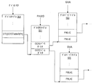
図2は、複数のプロセッサノード間のHyperTransport(商標)(HT)コヒーレントリンク61と、プロセッサノード及びI/Oデバイスの間のHT_I/Oリンク(例えば70A及び70B)とを用いるシステムの実施形態の1つの例である。より特定的には、1つの実施形態においては、HT_I/Oリンク(例えば71A)が、I/Oハブと他の周辺相互接続にブリッジするI/Oデバイスとの間で用いられてよい。加えて、任意の他のコヒーレント相互接続が複数のプロセッサノードの間で用いられてよく、且つ/又は任意の他のI/O相互接続がプロセッサノードとI/Oデバイスの間で用いられてよい。例えば、I/Oリンク71B、71C、及び71Dは種々の実施形態においてPCIeリンクであってよい。また、別の例はノースブリッジに結合されるプロセッサを含んでいてよく、ノースブリッジは、伝統的なPC設計においてはメモリ及び1つ以上のI/O相互接続に更に結合される。
FIG. 2 illustrates an embodiment of a system that uses a HyperTransport ™ (HT)
図2に示される実施形態を参照すると、システム10aは処理ノード60A〜60Bを備えており、処理ノード60A〜60Bはそれぞれプロセッサ12A〜12Bを備えており、更にプロセッサ12A〜12BはそれぞれMMU14A〜14Bを備えている。処理ノード60A〜60Bはまた、メモリ制御器18A〜18Bを備えている。プロセッサ12A〜12Bの各々は、上述したプロセッサ12の例であってよい。同様にMMU14A〜14B及びメモリ制御器18A〜18Bの各々は、図1におけるMMU14及びメモリ制御器18の例であってよい。図示される実施形態においては、MMU機能性はプロセッサ内に組み込まれている。
Referring to the embodiment shown in FIG. 2, the
システム10aは、メモリ20A〜20Bを備えている分散メモリシステムを含む。システム物理アドレス空間は、メモリ20A〜20Bにわたって分散されていてよい。従って、所与のアドレスを指定している所与のメモリ要求は、その所与のアドレスが割り当てられているメモリ20A又は20Bに結合されるメモリ制御器18A又は18Bに経路付けられる。
I/Oデバイス(例えば図2に示されるI/Oハブ62A〜62Bに結合されるI/Oデバイス22A〜22D)からのメモリ要求は、当該メモリ要求をサービスすることになるメモリ制御器18A〜18Bに到達するのに全て同じパスをとらなくてよい。例えばI/Oデバイス22A〜22Bはメモリ要求をI/Oハブ62Aへ送信してよく、I/Oハブ62Aはそれらの要求を処理ノード60Aへ送信する。所与のメモリ要求のアドレスがメモリ20Bに割り当てられている場合、処理ノード60Aはその所与のメモリ要求を処理ノード60Bへ送信してよく、その結果、メモリ制御器18Bがその要求を受信して処理することができる。I/Oデバイス22C〜22Dはメモリ要求をI/Oハブ62Bへ送信してよく、I/Oハブ62Bはそれらの要求を処理ノード60Bへ送信してよい。所与のメモリ要求のアドレスがメモリ20Aに割り当てられている場合、処理ノード60Bはその所与のメモリ要求を処理ノード60Aへ送信してよい。
Memory requests from I / O devices (e.g., I / O devices 22A-22D coupled to I / O hubs 62A-62B shown in FIG. 2) are
IOMMUは、I/Oソースのメモリ要求とメモリ20の間のパスに沿ってどこにあってもよい。図示される実施形態においては、IOMMU26A〜26Bは、I/Oハブ62A〜62B内に含まれている。従って、対応するハブに結合されるI/Oデバイスによって供給される任意のメモリ要求は、そのI/Oハブ内のIOMMUによってトランスレートされてよい。他の実施形態は、IOMMUを、I/Oデバイス内のIOTLBから処理ノード60A〜60B内のIOMMUまでの、更にはメモリ制御器18A〜18BにおけるIOMMUまでの異なる場所に置いてよい。更に、IOMMUは、システムの異なる部分における異なる点に位置していてよい。例えば幾つかの実施形態においては、I/Oデバイスは、図示されるようなローカルメモリ24Dを含み得るデバイスであってよい。従ってI/Oデバイス22Dはまた、ローカル/プライベートMMU23Dを含む。
The IOMMU can be anywhere along the path between the memory request of the I / O source and the memory 20. In the illustrated embodiment,
図3を参照すると、I/Oトランスレーションテーブル36の1つの実施形態を説明する図が示されている。具体的には、I/Oトランスレーションテーブル36は、デバイステーブル36A、インターラプト再マッピングテーブル36B、及び2セットのI/Oページテーブル(例えば36C及び36D)を含んでいてよい。制御レジスタ32の1つ(制御レジスタ32A)もまた、図3に示されている。制御レジスタ32Aは、デバイステーブル36Aのベースアドレスを記憶していてよい。 Referring to FIG. 3, a diagram illustrating one embodiment of the I / O translation table 36 is shown. Specifically, the I / O translation table 36 may include a device table 36A, an interrupt remapping table 36B, and two sets of I / O page tables (eg, 36C and 36D). One of the control registers 32 (control register 32A) is also shown in FIG. The control register 32A may store the base address of the device table 36A.
デバイステーブル36Aは、デバイスに割り当てられたデバイスIDによって索引付けられる複数のエントリを含む。従って、所与のデバイスはデバイステーブル36A内のエントリの1つに対応する(但し、デバイスが多重デバイスIDを有する場合を除き、又はデバイスがブリッジデバイスで他と集約されたトラフィックを有し且つそのトラフィックがそのブリッジのデバイスIDの下で送信される場合を除く)。デバイステーブルエントリは種々のデータを含み得る。例示的なデバイステーブルエントリ325の部分が図4に示されており、以下に更に詳細に説明される。
The device table 36A includes a plurality of entries that are indexed by the device ID assigned to the device. Thus, a given device corresponds to one of the entries in the device table 36A (unless the device has multiple device IDs, or the device has traffic aggregated with others at the bridge device and its Unless traffic is sent under the device ID of the bridge). The device table entry may contain various data. A portion of an exemplary
所与のデバイステーブルエントリ325は、I/Oページテーブル36C及び36Dへのポインタ(矢印301及び302によって示される)を含んでいてよい。ポインタは、I/Oページテーブル36C又は36D内でトランスレーション検索するための開始点であるページテーブルを指し示すことができる。図示されるように、開始ページテーブルは、上述したように、他のページテーブルへのポインタを階層的な形態で含んでいてよい。以下に更に説明されるように、実装されたトランスレーション処理に従って、幾つかのテーブルはPASIDによって索引付けられていてよい一方で、他のテーブルは、トランスレートされるべきゲスト仮想アドレス又はゲスト物理アドレスのいずれかの種々のビットを用いて索引付けられてよい。
A given
デバイステーブルエントリ325はまた、インターラプト再マッピングテーブル36Bへのポインタを含んでいてよい(矢印304によって示される)。インターラプト再マッピングデータは、あるデバイスによってインターラプト要求が送信される場合に用いられてよく、そしてインターラプトIDによって索引付けられてよい。インターラプトIDは、要求されたインターラプトを識別するデータを備えていてよく、そしてインターラプト要求を送信するのに用いられるメカニズムに基づいて異なっていてよい。
尚、1つのデバイステーブル36Aが示されているが、所望により多重デバイステーブルが維持されていてもよい。制御レジスタ32A内のデバイステーブルベースアドレスは、他のデバイステーブルを指し示すために変化し得る。更に、デバイステーブルは、必要に応じて上述のページテーブルと同様に階層的であってよい。同様に、1つのインターラプト再マッピングテーブル36Bが示されているが、多重インターラプトマッピングテーブルが、例えばデバイステーブル36A内のエントリ毎に1つまであってよい。また、ページテーブルの多重セットが、例えばデバイステーブル36A内のエントリ毎に1つまであってよい。尚、互いに独立しているが、他の実施形態は、インターラプト再マッピング機能性なしにI/Oトランスレーション機能性を実装し得る。 Although one device table 36A is shown, a multiple device table may be maintained as desired. The device table base address in the control register 32A can change to point to other device tables. Furthermore, the device table may be hierarchical as necessary, similar to the page table described above. Similarly, although one interrupt remapping table 36B is shown, there may be one multiple interrupt mapping table for each entry in the device table 36A, for example. Further, there may be one page table multiple set for each entry in the device table 36A, for example. Although independent of each other, other embodiments may implement I / O translation functionality without interrupt remapping functionality.
図示される実施形態においては、I/Oトランスレーションテーブル36C及び36Dは、1レベル及び2レベルのゲストトランスレーションの種々の組み合わせをサポートし得る。点線によって示されるように、トランスレーションがゲスト(即ち2レベル)トランスレーションである場合(破線によって示される)、矢印301で始まるパスをたどる。一方、ゲストトランスレーションが有効でない場合には、矢印302で始まる実線のパスをたどる。
In the illustrated embodiment, I / O translation tables 36C and 36D may support various combinations of one-level and two-level guest translations. If the translation is a guest (ie two level) translation (indicated by a dashed line), as indicated by the dotted line, follow the path starting at
より特定的には、GVAを含むメモリアクセス要求又はトランスレーション要求がI/Oデバイスから受信されると、当該要求のデバイスIDに対応するデバイステーブルエントリがアクセスされる。より特定的には、当然ながら、GVAを発行するI/Oデバイスは、PASIDプレフィックスを含むことによってそれを表示し、またGPAを発行するI/Oデバイスは、PASIDプレフィックスを省略することによってそれを表示する。図5の説明と共に後で更に詳細に説明されるように、GCR3テーブル307のベースアドレスへのSPAポインタ(例えば301)が用いられ、またGCR3テーブル307内へ索引付けて所与のデバイス上で動作中の1つ以上の処理を区別するためにPASIDが用いられてよい。GCR3テーブル307内のエントリは、GCR3ページテーブル311のベースへのGPAポインタを含んでいてよい。しかし、テーブル内のこのGPAポインタ及び後続の全てのGPAポインタは、例えばメモリ内の次のページテーブルにアクセスするために、トランスレーション論理及びページテーブルのセット、例えばテーブル333及び335を用いてSPAへとトランスレートされてよい。このトランスレーションメカニズムは、図3においてGPA/SPAトランスレーションユニット309A、309B、309C、及び309Dによって表されている。要求のGVAの幾つかの数のビットが、GCR3ページテーブル311内へ索引付けるために用いられてよい。1つの実施形態においては、311内の対応するエントリは、ページマップレベル4(PML4)ページテーブル313のベースへのGPAポインタを含んでいてよい。入れ子にされたページテーブルの各々におけるその後のアドレスもまた、次のページのベースアドレスを指し示すGPAであってよく、あるいは最後のテーブル(例えば315)である場合には、エントリは物理メモリページへのGPAポインタを含んでいてよい。これらのテーブルの各々(例えば313,315)はまた、I/O要求のGVAによって索引付けられていてよい。最終的なトランスレーション(SPA)は、GVAの一部分(例えば最後の数ビット)とメモリ317内の物理ページのSPAとを連結させることによって得られるであろう。
More specifically, when a memory access request or translation request including GVA is received from an I / O device, a device table entry corresponding to the device ID of the request is accessed. More specifically, of course, an I / O device issuing a GVA indicates it by including a PASID prefix, and an I / O device issuing a GPA designates it by omitting the PASID prefix. indicate. As described in more detail later in conjunction with FIG. 5, an SPA pointer (eg, 301) to the base address of the GCR3 table 307 is used and indexed into the GCR3 table 307 to operate on a given device. PASID may be used to distinguish one or more processes within. The entry in the GCR3 table 307 may include a GPA pointer to the base of the GCR3 page table 311. However, this GPA pointer in the table and all subsequent GPA pointers are sent to the SPA using the translation logic and a set of page tables, eg tables 333 and 335, to access the next page table in memory, for example. And may be translated. This translation mechanism is represented in FIG. 3 by GPA /
このように、ゲストトランスレーションテーブル及び入れ子にされたトランスレーションテーブルの両方が2レベルのゲストトランスレーションにおいて用いられてよい。しかし、GPAがI/Oデバイスによって提供される場合には、ホストトランスレーションページテーブル36Dのベースアドレスを提供するポインタ302を用いることによって、1レベルのトランスレーションが行われてもよい。より特定的には、デバイステーブルエントリにおけるゲスト情報は無視され、そして他のページテーブル経路付けエントリ情報(図4に示される)が、対応するホストトランスレーションページテーブルにアクセスするために用いられてよい。トランスレーションの種々のレベルにおいて、各連続するページテーブル内へ索引付けるために、GPAの異なるサブセットのビットが用いられ得る。特に、ポインタ302は、PML4ページテーブル333のベースへのSPAポインタであってよい。ゲストテーブル36Cとは対照的に、ホストページテーブル36D内の各ポインタは、次のテーブルのベースを指し示すSPAであってよい。PML4ページテーブル333内のGPAによって索引付けられるエントリは、PML3/2ページテーブル335のベースへのSPAポインタを含む。実際のページテーブルレベル(即ち3又は2)に応じて、テーブル335のエントリ内のポインタは、次のテーブルへのSPAポインタ又は物理メモリページ337のSPAであってよい。従って、最終的なトランスレーション(SPA)は、GPAの一部分(例えば最後の数ビット)とメモリ337内の物理ページのSPAとを連結させることによって得られるであろう。
Thus, both guest translation tables and nested translation tables may be used in two levels of guest translation. However, if the GPA is provided by an I / O device, one level of translation may be performed by using the
メモリ隔離を保つために、1つの実施形態では、各後続のページテーブルにアクセスするときに、許可がチェックされてよく、そして許可矛盾があり又はページが存在しない場合には、IOMMU26は、トランスレーション及び/又はルックアップを停止し、そしてページフォールトを内部的に発行すると共にエラーを記録してよい。他の実施形態においては、各段階で、IOMMUは任意のエラーを単純に累積して、トランスレーションの最後にトランスレーションを破棄し、ページフォールトを発行し、そしてエラーを記録してよく、あるいはこれらの何らかの組み合わせを行ってよい。
To maintain memory isolation, in one embodiment, when accessing each subsequent page table, permissions may be checked, and if there is a permission conflict or the page does not exist, the
図4を参照すると、例示的なデバイステーブルエントリの1つの実施形態の図が示されている。尚、図4の実施形態において示されるフィールドは、インターラプト再マッピング及び/又はアドレストランスレーションに関係していてよく、そして種々の実施形態において他の目的のために他のフィールドが提供されてよい。図示される実施形態においては、デバイステーブルエントリ325は256ビットエントリである。しかし、他の実施形態は、フィールド及び他のフィールドのスーパーセット、フィールドのサブセット、又は他のフィールドとの組み合わせにおけるサブセットを実装していてよい。従ってデバイステーブルエントリ325は、所望に応じて任意の数のビットであってよい。フィールドは1つ以上のビットを備えていてよく、そのエンコーディングは、IOMMU26によって解釈されるときに特定の意味を割り当てられている。この実施形態に対してフィールドが単一ビットである場合には、それは1ビット(a bit)と称されることがある。しかし、他の実施形態においては、同様の目的のために多重ビットフィールドが用いられてよい。この実施形態のために、図4に示されるビット範囲を有する多重ビットフィールドが示されている。
Referring to FIG. 4, a diagram of one embodiment of an exemplary device table entry is shown. Note that the fields shown in the embodiment of FIG. 4 may relate to interrupt remapping and / or address translation, and other fields may be provided for other purposes in various embodiments. . In the illustrated embodiment,
特定のインターラプトがブロックされ又は修正されずに通過させられるのかを制御するために、種々の特定のインターラプト制御ビットがResaeved_and_Otherフィールド内に設けられていてよい。ゲスト進歩的プログラム可能インターラプト制御器(guest advanced programmable interrupt controller)(GAPIC)に対するサポートが、GAPICTableRtPtrフィールドによって提供されており、GAPICTableRtPtrフィールドは、デバイスのためのGAPICテーブルのベースアドレスのSPAを含む。インターラプトテーブルポインタフィールド(IntTablePtr)は、上述のインターラプト再マッピングテーブルのベースアドレスを記憶していてよい。インターラプトテーブル長(IntTableLen)は、インターラプトテーブルの範囲を指定する。インターラプトテーブル長フィールドは、様々な可能な長さ(例えば1つの実施形態のためには、2のべき乗で1〜2048)に対してエンコードされ得る。インターラプトメッセージに対してI/Oページフォールトが検出された場合に、イベントログバッファ44内のイベントログエントリが作成されるか否かを表示するために、IGビットが用いられてよい。インターラプト有効(IV)ビットは、インターラプト関連フィールドが有効であるか否かを表示してよい。フィールドが有効でない場合には、IOMMU26は全てのインターラプトを修正せずに通過させてよい。
Various specific interrupt control bits may be provided in the Reserved_and_Other field to control whether specific interrupts are blocked or passed through without modification. Support for the guest advanced programmable interrupt controller (GAPIC) is provided by the GAPICTableRtPtr field, which contains the SPA for the base address of the GAPIC table for the device. The interrupt table pointer field (IntTablePtr) may store the base address of the interrupt remapping table described above. The interrupt table length (IntTableLen) specifies the range of the interrupt table. The interrupt table length field may be encoded for a variety of possible lengths (eg, 1-powered 1 to 2048 for one embodiment). The IG bit may be used to indicate whether an event log entry in the event log buffer 44 is created when an I / O page fault is detected for the interrupt message. The interrupt valid (IV) bit may indicate whether the interrupt related field is valid. If the field is not valid,
ゲストCR3(GCR3)テーブルルートポインタ(GCR3TableRtPtr)フィールドは、I/Oデバイスに対するCR3テーブルのSPAを含んでいてよい。周辺ページサービス要求(PPR)ビットは、IOMMUが周辺ページサービス要求ログエントリへ変換する周辺ページサービス要求を周辺機器が発行してよいかどうか、あるいは要求がエラーとして取り扱われるかどうかを表示する。尚、GCR3TableRtPtrは、図示される実施形態においては多重フィールドに分解されているが、他の実施形態においては、GCR3TableRtPtrは、1つの連続的なフィールドであってよく、あるいは所望に応じて異なるように分解されてよい。 The guest CR3 (GCR3) table root pointer (GCR3TableRtPtr) field may contain the SPA of the CR3 table for the I / O device. The peripheral page service request (PPR) bit indicates whether the peripheral device may issue a peripheral page service request that the IOMMU converts into a peripheral page service request log entry, or whether the request is treated as an error. Note that GCR3TableRtPtr is broken down into multiple fields in the illustrated embodiment, but in other embodiments, GCR3TableRtPtr may be one continuous field, or different as desired. May be disassembled.
SysMgtフィールドは、システム管理範囲における通信の更なる制御を提供するためにエンコードされてよい。具体的には、1つの実施形態においては、SysMgtフィールドは、当該範囲内の要求をブロックし、当該範囲内の要求を修正せずに転送し(ポストされた書き込みのみ)、INTxメッセージへマッピングしている要求を修正せずに転送し(ポストされた書き込みのみ)、又はI/Oページテーブルを用いて要求をトランスレートするようにエンコードされてよい。IoCtlフィールドは、I/O空間範囲における通信の更なる制御を提供するためにエンコードされてよい。具体的には、1つの実施形態においては、IoCtlフィールドは、当該範囲内の要求をブロックし、要求を修正せずに転送し、又はI/Oページテーブルを用いて要求をトランスレートするようにエンコードされてよい。しかし、1つの実施形態においては、これらのフィールドの幾つか(例えばSysMgt、IoCtl)は、GPA−SPAトランスレーションのみに関連している一方、GVA−SPAトランスレーションには適用されない。 The SysMgt field may be encoded to provide further control of communications in the system management range. Specifically, in one embodiment, the SysMgt field blocks requests within the range, forwards requests within the range without modification (posted writes only), and maps to INTx messages. The request may be forwarded without modification (posted writes only) or encoded to translate the request using an I / O page table. The IoCtl field may be encoded to provide further control of communications in the I / O space range. Specifically, in one embodiment, the IoCtl field blocks requests within that range, forwards the request without modification, or translates the request using an I / O page table. May be encoded. However, in one embodiment, some of these fields (eg, SysMgt, IoCtl) are only relevant for GPA-SPA translation, but not for GVA-SPA translation.
DomainIDは、異なるデバイスがそれらのトランスレーションデータを区別するように、キャッシュ30エントリとIOMMU26内の任意の他のキャッシュエントリとをタグ付けるために用いられる。複数のデバイスがトランスレーションテーブルを共有する場合に、それらは同じDomainIDを用いてキャッシュエントリを共有することができる。DomainIDは完全にソフトウエアの制御の支配下にあり、従って制御ソフトウエア(例えば仮想マシンモニタ、又は非仮想マシン実装におけるオペレーティングシステム)に対する柔軟性を許容して、I/Oデバイスを、トランスレーションデータを共有する又はデバイスを隔てるドメインへとグループ化することができる。例えば、所与の仮想マシンに割り当てられたデバイスは同じDomainIDを有していてよく、そして異なるDomailIDは異なる仮想マシンに対して用いられてよい。従って、隔てられた複数のデバイス及びグループ化された複数のデバイスの任意の組み合わせが創出されてよい。
The DomainID is used to tag the cache 30 entry and any other cache entry in the
1つの実施形態においては、ゲストCR3レベル(GLX)ビットは、IOMMUによって実行されることになるGCR3ルックアップの種類(即ち1レベル又は2レベルのGCR3テーブル)を指定する。ゲストトランスレーション有効(GV)ビットは、2レベル(即ち入れ子にされ且つゲストのレベル)トランスレーション又は1レベル(例えばホスト)トランスレーションのどちらが実行されることになるかを決定する。1つの実施形態においては、GVビットがクリアである場合、GLXビットフィールド及びGCR3TableRtPtrフィールドは無視される。 In one embodiment, the guest CR3 level (GLX) bit specifies the type of GCR3 lookup that is to be performed by the IOMMU (ie, a 1-level or 2-level GCR3 table). The guest translation valid (GV) bit determines whether a two level (ie nested and guest level) translation or a one level (eg host) translation will be performed. In one embodiment, if the GV bit is clear, the GLX bit field and the GCR3TableRtPtr field are ignored.
ページテーブルポインタ(PageTablePtr)は、ホストトランスレーションページテーブル36Dへのポインタである。このポインタは、I/OデバイスがGPAを提供する場合に用いられてよい。モードフィールド(Mode)は、デバイスのI/Oページテーブルの深さ、及びトランスレーションが完全に無効にされているかどうかを表示するためにコード化されてよい。例えば、SPAを提供し且つ要求が事前にトランスレートされたものとしてマークしているデバイスに対して、対応するデバイスエントリは、トランスレーションを無効にするためにエンコードされたこのフィールドを有していてよい。他のエンコーディングは、このエントリにマッピングされている要求に対してトランスレーションが開始することになるページテーブル階層内のレベルを表示してよい。TVビットは、ページトランスレーションデータが有効であるか否かを表示し、そしてVビットはエントリ80が有効であるかどうかを表示する。
The page table pointer (PageTablePtr) is a pointer to the host translation page table 36D. This pointer may be used when the I / O device provides the GPA. The Mode field (Mode) may be coded to indicate the depth of the device's I / O page table and whether translation is completely disabled. For example, for a device that provides SPA and the request is marked as pre-translated, the corresponding device entry has this field encoded to disable translation Good. Other encodings may indicate the level in the page table hierarchy at which translation will begin for requests mapped to this entry. The TV bit indicates whether page translation data is valid, and the V bit indicates whether
図5を参照すると、ゲスト仮想アドレストランスレーションメカニズムの更に詳細な態様を表す図が示されている。上述したように、デバイステーブル36Aは、各々がGCR3TableRtPtrフィールドを含む幾つかのエントリ(DTE)を含んでいてよい。当該エントリに対してゲストトランスレーションが有効である場合、フィールドはメモリ内のゲストCR3テーブル501へのSPAポインタを含むことになる。図示されるように、GCR3テーブル501は、デバイスの要求に関連するPASID値によって索引付けられていてよい。上述したように、デバイスPASIDは、用いられているI/O相互接続の種類に応じて種々の方法で得られてよい。図7においては、PASIDプレフィックスの1つの実施形態が示されている。このPASIDプレフィックスは、プレフィックスを用いる種々の標準的なバスアーキテクチャにおいて用いられ得る。図8においては、PCIe相互接続のためのTLP_PASIDプレフィックスが示されている。従って、図7のPASIDプレフィックスは、図8の実施形態において、所与のデバイス内の処理を識別するために用いられ得る。 Referring to FIG. 5, a diagram representing a more detailed aspect of the guest virtual address translation mechanism is shown. As described above, the device table 36A may include several entries (DTE), each including a GCR3TableRtPtr field. If guest translation is enabled for the entry, the field will contain the SPA pointer to the guest CR3 table 501 in memory. As shown, the GCR3 table 501 may be indexed by PASID values associated with device requests. As described above, the device PASID may be obtained in various ways depending on the type of I / O interconnect being used. In FIG. 7, one embodiment of a PASID prefix is shown. This PASID prefix can be used in various standard bus architectures that use prefixes. In FIG. 8, a TLP_PASID prefix for PCIe interconnection is shown. Accordingly, the PASID prefix of FIG. 7 can be used to identify processes within a given device in the embodiment of FIG.
図示されるようにCR3テーブル501は、各々がGCR3ベースポインタを含む2つのエントリを有しており、GCR3ポインタは、上述したようにゲストページテーブル503及び505へのGPAポインタであってよい。図示される実施形態においては、ゲストページテーブル503及び505は、I/O要求のGVAによって索引付けられていてよい。更に、ゲストページテーブル503及び505内の各有効なエントリは、それぞれのページマップレベル4テーブルのベースアドレスへのGPAポインタを含んでいてよい。 As shown, CR3 table 501 has two entries, each containing a GCR3 base pointer, which may be a GPA pointer to guest page tables 503 and 505 as described above. In the illustrated embodiment, guest page tables 503 and 505 may be indexed by I / O request GVA. Further, each valid entry in guest page tables 503 and 505 may include a GPA pointer to the base address of the respective page map level 4 table.
1つの実施形態においては、GCR3テーブル501はメモリ内で連続的である必要がある。従って、多数のPASIDを有するシステムにおいては、メモリ管理が煩わしいものになる場合がある。そこで、代替的な実施形態では、GCR3テーブルは階層的な方法で実装されてよい。例えば、1つ以上の第2レベルGCR3テーブル(図示せず)が用いられてよい。そのような実施形態においては、第1レベルGCR3テーブルがGCR3ベーステーブルであってよく、そしてPASIDビットの第1のサブセットを用いて索引付けられてよい。第1レベルGCR3テーブル内の所与のエントリは、それぞれの第2レベルGCR3テーブルへのGPAポインタを含んでいてよい。第2レベルGCR3テーブルは、PASIDの第2のサブセットを用いて索引付けられてよい。第2レベルGCR3テーブルの各エントリは、テーブル503又は505のようなゲストページテーブルへのGPAポインタを含んでいてよい。このように、1レベル又は2レベルのGCR3テーブルのいずれを実装するかの選択は、用いられるPASIDの数に依存する。尚、種々の実施形態において、PASIDビットのサブセットは、所望に応じて重複していなくてよく、あるいはそれらは重複していてよい。 In one embodiment, the GCR3 table 501 needs to be contiguous in memory. Therefore, in a system having a large number of PASIDs, memory management may be troublesome. Thus, in an alternative embodiment, the GCR3 table may be implemented in a hierarchical manner. For example, one or more second level GCR3 tables (not shown) may be used. In such an embodiment, the first level GCR3 table may be a GCR3 base table and may be indexed with a first subset of PASID bits. A given entry in the first level GCR3 table may include a GPA pointer to the respective second level GCR3 table. The second level GCR3 table may be indexed with a second subset of PASID. Each entry in the second level GCR3 table may include a GPA pointer to a guest page table such as table 503 or 505. Thus, the choice of whether to implement a one-level or two-level GCR3 table depends on the number of PASIDs used. It should be noted that in various embodiments, the subset of PASID bits may not overlap as desired, or they may overlap.
図6を参照すると、図1〜図5に示されるシステムの実施形態の動作態様を説明するフロー図が示されている。図1〜図6を集合的に参照すると共に図6のブロック601において開始すると、I/O要求がIOMMU26によって受信される。例えば、要求は、例えばVMアプリケーションの1つ(例えば102)を代表して、DMAアクセスのようなI/Oメモリアクセス要求であってよい。代替的には、要求は、例えばリモートIOTLBを伴うI/Oデバイスによる例えばATSのようなトランスレーション要求であってよい。要求がメモリ要求でない場合には、動作はブロック604に示されるように進んでよい。一方、要求がメモリ要求である場合には、IOMMU26は、例えばオンボードMMUを有しているI/Oデバイスの場合のように要求が事前にトランスレートされているものとマークされているかどうかを決定してよい(ブロック602)。マークされている場合には、アドレスはSPAであろうから、なんらトランスレーションは必要ない。要求が事前にトランスレートされているものとマークされている場合には、IOMMU26は要求をメモリ制御器18へ提供してよい(ブロック603)。
Referring to FIG. 6, a flow diagram illustrating the operational aspects of the system embodiment shown in FIGS. 1-5 is shown. With reference collectively to FIGS. 1-6 and starting at
ブロック602に戻り、要求が事前にトランスレートされているものとマークされていない場合、又は要求がトランスレーション要求である場合には、IOMMU26は、トランスレーションのためにキャッシュ30内でルックアップを行ってよい(ブロック604)。トランスレーションが存在する場合には、IOMMU26は、そのトランスレーションを要求側へ返送してよく、又はそのトランスレーションをその要求と共にメモリ制御器18へ供給してよい(ブロック603)。
Returning to block 602, if the request has not been marked as previously translated, or if the request is a translation request,
一方、トランスレーションがキャッシュ30内に存在しない場合(ブロック604)、制御論理34と共にテーブルウォーカ28がI/Oトランスレーションテーブル36にアクセスしてよい。より特定的には、テーブルウォーカ34が、デバイステーブルベースレジスタ32Aにアクセスしてメモリ20内のデバイステーブルベースアドレスを獲得してよい。テーブルウォーカ28は、デバイステーブル36A内へ索引付けるためのデバイスIDを用いてよい(ブロック605)。要求がPASID値を含んでいる場合(ブロック606)、テーブルウォーカ28は、2レベルのゲストトランスレーションを実行してよい。より特定的には、1つの実施形態においては、I/O要求がTLP_PASIDプレフィックスを含む場合には、その要求に関連するアドレスはGVAである。従って、2レベルのトランスレーションが実行される。テーブルウォーカ28は、メモリ内のGCR3テーブルを見つけるために、デバイステーブルエントリ内のGCR3制御ビット及びGCR3TableRtPtrアドレスを用いてよい(ブロック607)。
On the other hand, if the translation is not in the cache 30 (block 604), the
上述したように、1つの実施形態においては、GCR3TableRtPtrアドレスはSPAであってよい。テーブルウォーカ28は、GPAポインタを用いて対応するGCR3テーブル及びゲストテーブルを見つけてよく、またPASIDを用いてGCR3テーブルを索引付けてよい。ブロック614に示されるように、また上述したように、各GPAポインタは、例えばホストトランスレーションページテーブル36Dを用いるIOMMU26によってトランスレートされてよい。要求のGVAビットの幾つかのサブセットが、単一又は複数のゲストページテーブルを索引付けるために用いられてよい。最後のゲストページテーブルは、ホストページマップレベル4テーブルのベースアドレスへのGPAポインタを含んでいてよい。1つの実施形態においては、各連続するゲストテーブルがアクセスされるのに従って許可がチェックされ、そして任意の失敗した許可は、ページフォールト又は他のエラーを生成してよい(ブロック608)。
As described above, in one embodiment, the GCR3TableRtPtr address may be SPA. The
テーブルウォーカ28は次いで、各先行するテーブルの各エントリ内のGPAポインタを用いて、ホストトランスレーションテーブル36Dを連続的に見つけることができる。ページテーブルの種々のレベルで、要求のGVAビットの異なるサブセットが、各ホストトランスレーションページテーブル内へ索引付けるために用いられてよい。上述したように、最後のページテーブルが一旦アクセスされると、対応するエントリは、メモリ内の物理ページのGPAを含むであろう。テーブルウォーカ28は、そのGPAをSPAへとトランスレートしてよい(ブロック609)。テーブルウォーカ28は次いで、物理メモリページのSPAをGVAの最後の幾つかのビットと連結させて、最終的なトランスレーションアドレスを獲得することができる(ブロック610)。テーブルウォーカ28は、要求がメモリ要求である場合には、トランスレーションアドレスを要求と共にメモリ制御器18へ提供してよい。代替的には、テーブルウォーカ28は、要求がトランスレーション要求であった場合には、要求しているI/Oデバイスへトランスレーションを提供してよい。テーブルウォーカ28はまた、将来のトランスレーションルックアップでの使用のために、キャッシュ30内のトランスレーションを記憶してよい(ブロック611)。
The
ブロック606に戻り、要求がPASIDを含んでいない場合には、要求におけるアドレスはGPAである。この場合、テーブルウォーカ28は、メモリ内のホストトランスレーションページテーブル36Dを見つけるために、デバイステーブルエントリ内のPageTableRtPtrアドレスを用いて1レベルのトランスレーションを実行してよい(ブロック612)。上述したのと同様の方法において、テーブルウォーカ28は、I/Oデバイスに対するホストページマップレベル4テーブルのベースアドレスへのSPAポインタを用いることができる。しかし、ゲストトランスレーションとは対照的に、ホストトランスレーションページテーブルを用いて1レベルのトランスレーションを行う場合には、次のページテーブル/メモリ物理ページへの各ポインタはSPAである。従って、テーブルウォーカ28は、各先行するテーブルの各エントリ内のSPAポインタを用いて、ホストトランスレーションテーブルを連続的に見つけることができる。ホストページテーブルの各レベルで、要求のGPAビットの異なるサブセットが、各ホストトランスレーションページテーブル内へ索引付けるために用いられてよい。上述したように、最後のページテーブルが一旦アクセスされると、対応するエントリは、メモリ内の物理ページのSPAを含むであろう(ブロック613)。テーブルウォーカ28は、物理メモリページのSPAを要求のGPAの最後の幾つかのビットと連結させて、最終的なトランスレーションアドレスを獲得することができる(ブロック610)。
Returning to block 606, if the request does not include a PASID, the address in the request is GPA. In this case, the
図7を参照すると、PASIDプレフィックスペイロード(payload)の1つの実施形態の図が示されている。図示されるように、PASIDプレフィックスペイロード701は24ビットを含む。図示される実施形態においては、ビット[15:0]はゲスト処理アドレス空間ID、ビット[21:16]は予備、ビット22は実行/非実行許可、そしてビット23はユーザ/スーパバイザ表示である。尚、他の実施形態においては、ビットの位置及び定義は異なっていてよい。また、他の実施形態においては、他のビットが他の属性を表示するために用いられてよい。例えば、ビットはキャッシュコヒーレンシや特別なセキュリティ属性を表示することがある。
Referring to FIG. 7, a diagram of one embodiment of a PASID prefix payload is shown. As shown, the
1つの実施形態においては、PASIDビットは、要求/デバイスIDと共に、トランザクションに関連するアドレス空間を一意的に識別する。実行/非実行ビットは、セットされているときに、表示されているメモリの範囲が、要求機能によって実行され得るコードを含んでいるであろうことを表示してよく、またビットをクリアしているときに、要求機能によって実行され得るコードがないことを表示してよい。ユーザ/スーパーバイザビットは、セットされているときに、表示されているメモリ範囲が、ユーザモード又はスーパーバイザモードで動作している構成要素によってアクセス可能な情報を含んでいるであろうことを表示してよい。一方、クリアにされているビットは、表示されているメモリ範囲が、スーパーバイザモードにおいてのみ動作している構成要素によってアクセス可能な情報を含んでいるであろうことを表示してよい。 In one embodiment, the PASID bit, together with the request / device ID, uniquely identifies the address space associated with the transaction. The execute / non-execute bit, when set, may indicate that the range of memory being displayed will contain code that can be executed by the request function, and clear the bit. May indicate that no code can be executed by the request function. The user / supervisor bit, when set, indicates that the displayed memory range will contain information accessible by components operating in user mode or supervisor mode. Good. On the other hand, a cleared bit may indicate that the displayed memory range will contain information accessible by components operating only in supervisor mode.
上述したように、多くの標準的な周辺バスアーキテクチャがプレフィックスを可能にする。従って、PASIDプレフィックスペイロード701は、それによってI/Oデバイスが制御されている最中であるところの処理の処理識別子を伝達するために用いられてよい。図8A及び図8Bの説明と共に以下で更に詳細に説明されるように、周辺バス/相互接続はPCIe相互接続であってよい。従って、PASIDプレフィックス701は、PCIeトランザクション層プロトコルパケット構造内で用いられてよい。
As mentioned above, many standard peripheral bus architectures allow prefixes. Accordingly, the
図8Aを参照すると、PCIe規格に従う例示的なTLPパケットの1つの実施形態の図が示されている。PCIeは、パケットベースのプロトコルを用いて、互いに通信する2つのデバイスのトランザクション層の間でPCIeリンクを介して情報を交換する。PCIeは、メモリ、I/O、構成、及びメッセージといった基本的なトランザクションの種類をサポートする。メモリ要求に対する2つのアドレシングフォーマット、32ビット及び64ビットがサポートされる。従って、図8Aに示されるように、TLPパケット801は、1つ以上の随意的なTLPプレフィックス、TLPヘッダ、データペイロード(幾つかの種類のパケットに対して)、及び随意的なTLPダイジェストを含む。パケットフィールド及びビットの定義に関する詳細な情報は、PCI−SIGから入手可能なPCIエクスプレス規格の最新バージョンにおいて見つかるであろう。とは言え、TLPプレフィックスの1つの具体的な実施形態のより詳細な説明が図8Bに示され、そして以下に説明される。
Referring to FIG. 8A, a diagram of one embodiment of an exemplary TLP packet according to the PCIe standard is shown. PCIe uses a packet-based protocol to exchange information over the PCIe link between the transaction layers of two devices communicating with each other. PCIe supports basic transaction types such as memory, I / O, configuration, and messages. Two addressing formats for memory requirements are supported, 32 bits and 64 bits. Thus, as shown in FIG. 8A, a
図8Bを参照すると、PCIe規格に従うTLP_PASIDプレフィックスの1つの実施形態の図が示されている。図7に示されるプレフィックスと同様に、TLPプレフィックス851は、上述したような16ビットPASIDフィールド、6ビット予備フィールド、上述のような実行ビット(exe bit)、上述のようなユーザビット、4ビットタイプフィールド、プレフィックスが終端間(end-to-end)であることを表示する1ビットフィールド、及びフォーマットフィールドを含む。図示されるように、フォーマットフィールドは、そのTLPプレフィックスがTLPプレフィックスであることを表示する100bエンコーディングでエンコードされてよい。タイプフィールドは、プレフィックスがPASIDプレフィックスであることを表示するためにエンコードされてよい。尚、他の実施形態においては、TLPプレフィックスは、他のフィールドを含んでいてよく、またフィールド内に他の数のビットを含んでいてよい。
Referring to FIG. 8B, a diagram of one embodiment of a TLP_PASID prefix according to the PCIe standard is shown. Similar to the prefix shown in FIG. 7, the
上述したように、1つの実施形態においては、キャッシュ30エントリから取り出される不十分なゲスト特権を結果としてもたらすATS(即ちトランスレーション)要求又はメモリ参照は、新鮮でない(stale)情報に基づいているであろう。キャッシュされたゲストトランスレーション情報を用いてIOMMU26がアクセス違反を検出すると、IOMMU26は、キャッシュされた情報を置換し又は廃棄する処理において、ゲストページテーブルを再ウォークして、メモリから読み出された新鮮な情報を用いてアクセス許可を再計算する必要がある。ゲストテーブル再ウォークの結果として、入れ子にされたページテーブルが読み出されてよい。フェッチされた情報が、アクセスを許可しない許可制御を含んでいる場合には、IOMMU26はアクセスに失敗し、そうでない場合にはIOMMU26は要求されたアクセスを許可してよい。ATSトランスレーション要求は、計算されたアクセス特権を常に返送する。再ウォークは、ゲストトランスレーション及び入れ子にされたトランスレーションの両方の完全なウォークを必要とすることがある。
As described above, in one embodiment, ATS (ie translation) requests or memory references that result in insufficient guest privileges being retrieved from the cache 30 entry are based on stale information. I will. When the
尚、PCIeデバイスを実装している実施形態においてアドレスをトランスレートする場合には、IOMMU26は、内部プロセッサセマンティクス(semantics)とPCIeセマンティクスの間での変換を必要とすることがある。種々のエージテーブルは存在ビット(P)及び読み出し/書き込みビット(R/W)を含み、ATS要求は非書き込みヒントを含み、そしてATS応答は別個の読み出し(R)許可ビット及び書き込み(W)許可ビットを必要とする。1つの実施形態においては、IOMMU26は、特権プロモーションのためのプロセッサ内部長ページテーブルセマンティクスと無矛盾なATS応答を提供してよい。概してIOMMU26は、キャッシュ30内で見つかる値に基づく結果を返送すべきである。ATS要求に対する特別な場合として、無効化コマンドをIOMMU26に発行することなしにシステムソフトウエアがアクセス許可を上げてしまった(have elevated)であろうページに対するものがある。1つの実施形態では、システムソフトウエアは、アクセス許可を減少させる場合に無効化コマンドを発行する必要がある(ページをP=0で非存在にマーキングすることを含む)。具体的には、ソフトウエアは、書き込み若しくは実行の許可を解除した後、Pを存在から非存在に変化させた後、又はU/Sをユーザからスーパーバイザに変化させた後に無効化する必要がある。
Note that when translating addresses in an embodiment that implements a PCIe device, the
尚、上述の実施形態は、ハードウエア、ソフトウエア、又は両方の組み合わせにおいて実装され得る。また、上述のハードウエア構成部品の種々のものは、ハードウエア記述(定義)言語で書かれたソフトウエアを用いて最初に設計され得る。従って、上述の実施形態を実装するために用いられる任意の命令は、種々のタイプの記憶装置に記憶されてよい。このように、種々の実施形態は、以上の説明に従って実装される命令及び/又はデータをコンピュータ可読記憶媒体に記憶することを更に含み得る。一般的に言えば、コンピュータ可読記憶媒体は、磁気媒体又は光学媒体のような記憶媒体又はメモリ媒体、例えばディスク、CD−ROM、DVD、揮発性又は不揮発性媒体、例えばRAM(例えばSDRAM、DDR_SDRAM、RDRAM、SRAM等)、ROM等を含んでいてよい。 Note that the above-described embodiments may be implemented in hardware, software, or a combination of both. Also, the various hardware components described above can be initially designed using software written in a hardware description (definition) language. Thus, any instructions used to implement the above-described embodiments may be stored in various types of storage devices. Thus, various embodiments may further include storing instructions and / or data implemented in accordance with the above description on a computer-readable storage medium. Generally speaking, a computer-readable storage medium is a storage medium or memory medium such as a magnetic medium or an optical medium, such as a disk, CD-ROM, DVD, volatile or non-volatile medium, such as a RAM (eg, SDRAM, DDR_SDRAM, RDRAM, SRAM, etc.), ROM, etc. may be included.
上述の実施形態はかなり詳細に説明されてきたが、上述の開示が完全に理解されるならば、多くの変形及び修正が当業者に明らかになるであろう。以下の特許請求の範囲は全てのそのような変形及び修正を包含するものとして解釈されることが意図されている。 Although the embodiments described above have been described in considerable detail, many variations and modifications will become apparent to those skilled in the art once the above disclosure is fully appreciated. It is intended that the following claims be construed to include all such variations and modifications.
Claims (21)
前記I/Oデバイスからの要求において受信されるアドレスをトランスレートするように構成される制御論理と、
前記制御論理に結合され完了したトランスレーションを記憶するように構成されるキャッシュメモリとを備え、
処理アドレス空間識別子(PASID)プレフィックスを含むトランザクション層プロトコル(TLP)パケットを前記要求において受信することに応答して、前記制御論理は2レベルのゲストトランスレーションを実行するように構成され、
前記制御論理は前記要求において受信される前記アドレスをトランスレートするためにゲストページテーブルのセットにアクセスするように構成され、最後のゲストページテーブル内のポインタは入れ子にされたページテーブルのセット内の第1のテーブルを指し示し、
前記制御論理は、入れ子にされたページテーブルの前記セットにアクセスして前記システムメモリ内の物理ページに対応するシステム物理アドレス(SPA)を得るために、最後のゲストページテーブル内の前記ポインタを用いるように構成されるIOMMU。 An input / output (I / O) memory management unit (IOMMU) for controlling requests by an I / O device to system memory of a computer system,
Control logic configured to translate an address received in a request from the I / O device;
A cache memory coupled to the control logic and configured to store completed translations;
In response to receiving a transaction layer protocol (TLP) packet including a processing address space identifier (PASID) prefix in the request, the control logic is configured to perform two levels of guest translation;
The control logic is configured to access a set of guest page tables to translate the address received in the request, and a pointer in the last guest page table is in a nested page table set Pointing to the first table,
The control logic uses the pointer in the last guest page table to access the set of nested page tables to obtain a system physical address (SPA) corresponding to the physical page in the system memory. IOMMU configured as follows.
前記プロセッサに結合されトランスレーションデータを記憶するように構成されるシステムメモリと、
前記システムメモリにアクセスするための要求を生成するように構成される少なくとも1つのI/Oデバイスと、
前記I/Oデバイス及び前記システムメモリに結合されるI/Oメモリ管理ユニット(IOMMU)と、
前記制御論理に結合され完了したトランスレーションを記憶するように構成されるキャッシュメモリとを備え、
前記IOMMUは前記I/Oデバイスからの前記要求において受信されるアドレスをトランスレートするように構成される制御論理を含み、
処理アドレス空間識別子(PASID)プレフィックスを含むトランザクション層プロトコル(TLP)パケットを前記要求において受信することに応答して、前記制御論理は2レベルのゲストトランスレーションを実行するように構成され、
前記制御論理は前記要求において受信される前記アドレスをトランスレートするためにゲストページテーブルのセットにアクセスするように構成され、最後のゲストページテーブル内のポインタは入れ子にされたページテーブルのセット内の第1のテーブルを指し示し、
前記制御論理は、入れ子にされたページテーブルの前記セットにアクセスして前記システムメモリ内の物理ページに対応するシステム物理アドレス(SPA)を得るために、最後のゲストページテーブル内の前記ポインタを用いるように構成されるシステム。 A processor;
A system memory coupled to the processor and configured to store translation data;
At least one I / O device configured to generate a request to access the system memory;
An I / O memory management unit (IOMMU) coupled to the I / O device and the system memory;
A cache memory coupled to the control logic and configured to store completed translations;
The IOMMU includes control logic configured to translate an address received in the request from the I / O device;
In response to receiving a transaction layer protocol (TLP) packet including a processing address space identifier (PASID) prefix in the request, the control logic is configured to perform two levels of guest translation;
The control logic is configured to access a set of guest page tables to translate the address received in the request, and a pointer in the last guest page table is in a nested page table set Pointing to the first table,
The control logic uses the pointer in the last guest page table to access the set of nested page tables to obtain a system physical address (SPA) corresponding to the physical page in the system memory. System configured as follows.
前記I/Oデバイスからの要求において受信されるアドレスをトランスレートするように構成される制御論理と、
前記制御論理に結合され完了したトランスレーションを記憶するように構成されるキャッシュメモリとを備え、
処理アドレス空間識別子(PASID)プレフィックスを含むトランザクション層プロトコル(TLP)パケットを前記要求において受信することに応答して、前記制御論理はシステムメモリ内に記憶されるトランスレーションデータを用いて2レベルのゲストトランスレーションを実行するように構成され、
前記トランスレーションデータは、デバイスデータ構造内の1つ以上のデバイステーブルエントリと、ゲストページデータ構造のセット及び入れ子にされたページデータ構造のセットを含んでいるI/Oページデータ構造の第1のセットとを含み、
前記制御論理は、
所与の要求を生成するI/Oデバイスに対応するデバイス識別子を用いて前記要求に対するデバイスデータ構造エントリを選択し、
選択されたデバイスデータ構造エントリからのポインタを用いてゲストトランスレーションデータ構造のセットにアクセスし、
最後のゲストトランスレーションデータ構造からのポインタを用いて、入れ子にされたページデータ構造の前記セットにアクセスするように更に構成されるIOMMU。 An input / output (I / O) memory management unit (IOMMU) for controlling requests by an I / O device to system memory of a computer system,
Control logic configured to translate an address received in a request from the I / O device;
A cache memory coupled to the control logic and configured to store completed translations;
In response to receiving a transaction layer protocol (TLP) packet including a processing address space identifier (PASID) prefix in the request, the control logic uses the translation data stored in system memory to Configured to perform translations,
The translation data includes a first I / O page data structure including one or more device table entries in the device data structure and a set of guest page data structures and a set of nested page data structures. Including set and
The control logic is
Selecting a device data structure entry for the request using a device identifier corresponding to the I / O device generating the given request;
Access a set of guest translation data structures using a pointer from the selected device data structure entry,
An IOMMU that is further configured to access the set of nested page data structures using a pointer from the last guest translation data structure.
ゲストページテーブルのセット及び入れ子にされたページテーブルのセットを含むトランスレーションデータをコンピュータシステムのシステムメモリ内に記憶することと、
処理アドレス空間識別子(PASID)プレフィックスを含むトランザクション層プロトコル(TLP)パケットをI/Oデバイスからの要求において受信することに応答して2レベルのゲストトランスレーションを実行するように構成される制御論理が、前記要求において受信されるアドレスをトランスレートすることと、
前記制御論理が前記要求において受信される前記アドレスをトランスレートするためにゲストページテーブルの前記セットにアクセスすることと、
完了したトランスレーションを前記制御論理がキャッシュメモリ内に記憶することとを備え、
最後のゲストページテーブル内のポインタは入れ子にされたページテーブルの前記セット内の第1のテーブルを指し示し、
前記制御論理は、入れ子にされたページテーブルの前記セットにアクセスして前記システムメモリ内の物理ページに対応するシステム物理アドレス(SPA)を得るために、最後のゲストページテーブル内の前記ポインタを用いる方法。 A method for controlling input / output I / O requests to system memory of a computer system using an input / output memory management unit (IOMMU) comprising:
Storing translation data in the system memory of the computer system including a set of guest page tables and a set of nested page tables;
Control logic configured to perform two levels of guest translation in response to receiving a transaction layer protocol (TLP) packet including a processing address space identifier (PASID) prefix in a request from an I / O device. Translating the address received in the request;
Accessing the set of guest page tables to translate the address received by the control logic in the request;
The control logic storing completed translations in a cache memory;
The pointer in the last guest page table points to the first table in the set of nested page tables;
The control logic uses the pointer in the last guest page table to access the set of nested page tables to obtain a system physical address (SPA) corresponding to the physical page in the system memory. Method.
前記データ構造において記述される前記回路は、
前記I/Oデバイスからの要求において受信されるアドレスをトランスレートするように構成される制御論理と、
前記制御論理に結合され完了したトランスレーションを記憶するように構成されるキャッシュメモリとを備え、
処理アドレス空間識別子(PASID)プレフィックスを含むトランザクション層プロトコル(TLP)パケットを前記要求において受信することに応答して、前記制御論理は2レベルのゲストトランスレーションを実行するように構成され、
前記制御論理は前記要求において受信される前記アドレスをトランスレートするためにゲストページテーブルのセットにアクセスするように構成され、最後のゲストページテーブル内のポインタは入れ子にされたページテーブルのセット内の第1のテーブルを指し示し、
前記制御論理は、入れ子にされたページテーブルの前記セットにアクセスして前記システムメモリ内の物理ページに対応するシステム物理アドレス(SPA)を得るために、最後のゲストページテーブル内の前記ポインタを用いるように構成されるコンピュータ可読記憶媒体。 A computer-readable storage medium having a data structure, wherein when the data structure is operated by a program executable on a computer system, the program operates based on the data structure and is described by the data structure Performing part of the process for manufacturing an integrated circuit including
The circuit described in the data structure is:
Control logic configured to translate an address received in a request from the I / O device;
A cache memory coupled to the control logic and configured to store completed translations;
In response to receiving a transaction layer protocol (TLP) packet including a processing address space identifier (PASID) prefix in the request, the control logic is configured to perform two levels of guest translation;
The control logic is configured to access a set of guest page tables to translate the address received in the request, and a pointer in the last guest page table is in a nested page table set Pointing to the first table,
The control logic uses the pointer in the last guest page table to access the set of nested page tables to obtain a system physical address (SPA) corresponding to the physical page in the system memory. A computer-readable storage medium configured as follows.
Applications Claiming Priority (3)
| Application Number | Priority Date | Filing Date | Title |
|---|---|---|---|
| US12/508,890 US9535849B2 (en) | 2009-07-24 | 2009-07-24 | IOMMU using two-level address translation for I/O and computation offload devices on a peripheral interconnect |
| US12/508,890 | 2009-07-24 | ||
| PCT/US2010/043168 WO2011011768A1 (en) | 2009-07-24 | 2010-07-24 | Iommu using two-level address translation for i/o and computation offload devices on a peripheral interconnect |
Publications (2)
| Publication Number | Publication Date |
|---|---|
| JP2013500524A true JP2013500524A (en) | 2013-01-07 |
| JP5680642B2 JP5680642B2 (en) | 2015-03-04 |
Family
ID=43013181
Family Applications (1)
| Application Number | Title | Priority Date | Filing Date |
|---|---|---|---|
| JP2012521868A Active JP5680642B2 (en) | 2009-07-24 | 2010-07-24 | IOMMU with two-level address translation for I / O and computational load reduction devices in peripheral interconnects |
Country Status (7)
| Country | Link |
|---|---|
| US (1) | US9535849B2 (en) |
| EP (1) | EP2457165B1 (en) |
| JP (1) | JP5680642B2 (en) |
| KR (1) | KR101575827B1 (en) |
| CN (1) | CN102498478B (en) |
| IN (1) | IN2012DN00935A (en) |
| WO (1) | WO2011011768A1 (en) |
Cited By (1)
| Publication number | Priority date | Publication date | Assignee | Title |
|---|---|---|---|---|
| US11754776B2 (en) | 2018-11-01 | 2023-09-12 | Kuraray Co., Ltd. | Light-emitting fiber |
Families Citing this family (72)
| Publication number | Priority date | Publication date | Assignee | Title |
|---|---|---|---|---|
| US8386745B2 (en) * | 2009-07-24 | 2013-02-26 | Advanced Micro Devices, Inc. | I/O memory management unit including multilevel address translation for I/O and computation offload |
| US8327055B2 (en) * | 2010-04-12 | 2012-12-04 | International Business Machines Corporation | Translating a requester identifier to a chip identifier |
| US8341340B2 (en) * | 2010-07-21 | 2012-12-25 | Seagate Technology Llc | Multi-tier address mapping in flash memory |
| US20120246381A1 (en) * | 2010-12-14 | 2012-09-27 | Andy Kegel | Input Output Memory Management Unit (IOMMU) Two-Layer Addressing |
| US9606936B2 (en) * | 2010-12-16 | 2017-03-28 | Advanced Micro Devices, Inc. | Generalized control registers |
| US9916257B2 (en) * | 2011-07-26 | 2018-03-13 | Intel Corporation | Method and apparatus for TLB shoot-down in a heterogeneous computing system supporting shared virtual memory |
| EP2756438B1 (en) * | 2011-09-13 | 2020-11-11 | Facebook, Inc. | Software cryptoprocessor |
| US8719464B2 (en) * | 2011-11-30 | 2014-05-06 | Advanced Micro Device, Inc. | Efficient memory and resource management |
| US20130262736A1 (en) * | 2012-03-30 | 2013-10-03 | Ati Technologies Ulc | Memory types for caching policies |
| US9081706B2 (en) * | 2012-05-10 | 2015-07-14 | Oracle International Corporation | Using a shared last-level TLB to reduce address-translation latency |
| US20140165196A1 (en) | 2012-05-22 | 2014-06-12 | Xockets IP, LLC | Efficient packet handling, redirection, and inspection using offload processors |
| WO2013177310A2 (en) | 2012-05-22 | 2013-11-28 | Xockets IP, LLC | Offloading of computation for rack level servers and corresponding methods and systems |
| US20140052899A1 (en) * | 2012-08-18 | 2014-02-20 | Yen Chih Nan | Memory address translation method for flash storage system |
| US9424199B2 (en) * | 2012-08-29 | 2016-08-23 | Advanced Micro Devices, Inc. | Virtual input/output memory management unit within a guest virtual machine |
| US9069690B2 (en) * | 2012-09-13 | 2015-06-30 | Intel Corporation | Concurrent page table walker control for TLB miss handling |
| KR101934519B1 (en) | 2012-11-26 | 2019-01-02 | 삼성전자주식회사 | Storage device and data transfering method thereof |
| US9378161B1 (en) | 2013-01-17 | 2016-06-28 | Xockets, Inc. | Full bandwidth packet handling with server systems including offload processors |
| US9250954B2 (en) | 2013-01-17 | 2016-02-02 | Xockets, Inc. | Offload processor modules for connection to system memory, and corresponding methods and systems |
| US9396011B2 (en) | 2013-03-12 | 2016-07-19 | Qualcomm Incorporated | Algorithm and apparatus to deploy virtual machine monitor on demand |
| US9477603B2 (en) | 2013-09-05 | 2016-10-25 | Facebook, Inc. | System and method for partitioning of memory units into non-conflicting sets |
| US9983894B2 (en) | 2013-09-25 | 2018-05-29 | Facebook, Inc. | Method and system for providing secure system execution on hardware supporting secure application execution |
| US10049048B1 (en) | 2013-10-01 | 2018-08-14 | Facebook, Inc. | Method and system for using processor enclaves and cache partitioning to assist a software cryptoprocessor |
| US9239804B2 (en) * | 2013-10-03 | 2016-01-19 | Advanced Micro Devices, Inc. | Back-off mechanism for a peripheral page request log |
| US9747450B2 (en) | 2014-02-10 | 2017-08-29 | Facebook, Inc. | Attestation using a combined measurement and its constituent measurements |
| US9734092B2 (en) | 2014-03-19 | 2017-08-15 | Facebook, Inc. | Secure support for I/O in software cryptoprocessor |
| EP3159802B1 (en) | 2014-07-15 | 2018-05-23 | Huawei Technologies Co. Ltd. | Sharing method and device for pcie i/o device and interconnection system |
| US20160077981A1 (en) * | 2014-09-12 | 2016-03-17 | Advanced Micro Devices, Inc. | Method and Apparatus for Efficient User-Level IO in a Virtualized System |
| US9632948B2 (en) * | 2014-09-23 | 2017-04-25 | Intel Corporation | Multi-source address translation service (ATS) with a single ATS resource |
| KR102320044B1 (en) * | 2014-10-02 | 2021-11-01 | 삼성전자주식회사 | Pci device, interface system including same, and computing system including same |
| US10013385B2 (en) * | 2014-11-13 | 2018-07-03 | Cavium, Inc. | Programmable validation of transaction requests |
| JP6070732B2 (en) * | 2015-01-27 | 2017-02-01 | 日本電気株式会社 | INPUT / OUTPUT CONTROL DEVICE, INPUT / OUTPUT CONTROL SYSTEM, INPUT / OUTPUT CONTROL METHOD, AND PROGRAM |
| US9495303B2 (en) | 2015-02-03 | 2016-11-15 | Intel Corporation | Fine grained address remapping for virtualization |
| CN104598298A (en) * | 2015-02-04 | 2015-05-06 | 上海交通大学 | Virtual machine dispatching algorithm based on task load and current work property of virtual machine |
| CN104698709A (en) * | 2015-04-01 | 2015-06-10 | 上海天马微电子有限公司 | Array substrate and liquid crystal display panel |
| US10089275B2 (en) * | 2015-06-22 | 2018-10-02 | Qualcomm Incorporated | Communicating transaction-specific attributes in a peripheral component interconnect express (PCIe) system |
| CN108027642B (en) | 2015-06-24 | 2021-11-02 | 英特尔公司 | System and method for isolating input/output computing resources |
| US10102116B2 (en) | 2015-09-11 | 2018-10-16 | Red Hat Israel, Ltd. | Multi-level page data structure |
| WO2017049590A1 (en) | 2015-09-25 | 2017-03-30 | Intel Corporation | Systems and methods for input/output computing resource control |
| US9852107B2 (en) * | 2015-12-24 | 2017-12-26 | Intel Corporation | Techniques for scalable endpoint addressing for parallel applications |
| US10509729B2 (en) | 2016-01-13 | 2019-12-17 | Intel Corporation | Address translation for scalable virtualization of input/output devices |
| US10055807B2 (en) | 2016-03-02 | 2018-08-21 | Samsung Electronics Co., Ltd. | Hardware architecture for acceleration of computer vision and imaging processing |
| US10762030B2 (en) | 2016-05-25 | 2020-09-01 | Samsung Electronics Co., Ltd. | Storage system, method, and apparatus for fast IO on PCIE devices |
| EP3338194B1 (en) * | 2016-05-31 | 2022-12-07 | Avago Technologies International Sales Pte. Limited | Multichannel input/output virtualization |
| US10048881B2 (en) * | 2016-07-11 | 2018-08-14 | Intel Corporation | Restricted address translation to protect against device-TLB vulnerabilities |
| US10241931B2 (en) * | 2016-07-29 | 2019-03-26 | Advanced Micro Devices, Inc. | Controlling access to pages in a memory in a computing device |
| US20180088978A1 (en) * | 2016-09-29 | 2018-03-29 | Intel Corporation | Techniques for Input/Output Access to Memory or Storage by a Virtual Machine or Container |
| US10157277B2 (en) * | 2016-10-01 | 2018-12-18 | Intel Corporation | Technologies for object-oriented memory management with extended segmentation |
| US10417140B2 (en) * | 2017-02-24 | 2019-09-17 | Advanced Micro Devices, Inc. | Streaming translation lookaside buffer |
| US10120813B2 (en) * | 2017-03-08 | 2018-11-06 | Arm Limited | Address translation |
| US10380039B2 (en) * | 2017-04-07 | 2019-08-13 | Intel Corporation | Apparatus and method for memory management in a graphics processing environment |
| US10228981B2 (en) | 2017-05-02 | 2019-03-12 | Intel Corporation | High-performance input-output devices supporting scalable virtualization |
| US10528474B2 (en) * | 2017-09-06 | 2020-01-07 | International Business Machines Corporation | Pre-allocating cache resources for a range of tracks in anticipation of access requests to the range of tracks |
| CN109698845B (en) * | 2017-10-20 | 2020-10-09 | 华为技术有限公司 | Data transmission method, server, unloading card and storage medium |
| WO2019132976A1 (en) * | 2017-12-29 | 2019-07-04 | Intel Corporation | Unified address translation for virtualization of input/output devices |
| US20190227942A1 (en) * | 2018-01-24 | 2019-07-25 | Dell Products, Lp | System and Method to Handle I/O Page Faults in an I/O Memory Management Unit |
| US10990436B2 (en) * | 2018-01-24 | 2021-04-27 | Dell Products L.P. | System and method to handle I/O page faults in an I/O memory management unit |
| US11157635B2 (en) * | 2018-04-08 | 2021-10-26 | Qualcomm Incorporated | Secure interface disablement |
| US11474916B2 (en) | 2018-08-22 | 2022-10-18 | Intel Corporation | Failover of virtual devices in a scalable input/output (I/O) virtualization (S-IOV) architecture |
| US10929310B2 (en) | 2019-03-01 | 2021-02-23 | Cisco Technology, Inc. | Adaptive address translation caches |
| US11036649B2 (en) | 2019-04-04 | 2021-06-15 | Cisco Technology, Inc. | Network interface card resource partitioning |
| US11494211B2 (en) * | 2019-04-22 | 2022-11-08 | Advanced Micro Devices, Inc. | Domain identifier and device identifier translation by an input-output memory management unit |
| US10853263B1 (en) | 2019-07-23 | 2020-12-01 | Ati Technologies Ulc | Unified kernel virtual address space for heterogeneous computing |
| CN111290829B (en) * | 2020-01-15 | 2023-05-02 | 海光信息技术股份有限公司 | Access control module, virtual machine monitor and access control method |
| US11422944B2 (en) * | 2020-08-10 | 2022-08-23 | Intel Corporation | Address translation technologies |
| US11321238B2 (en) | 2020-08-11 | 2022-05-03 | Micron Technology, Inc. | User process identifier based address translation |
| US20210004338A1 (en) * | 2020-09-21 | 2021-01-07 | Pratik Marolia | Pasid based routing extension for scalable iov systems |
| US11775210B2 (en) * | 2020-10-14 | 2023-10-03 | Western Digital Technologies, Inc. | Storage system and method for device-determined, application-specific dynamic command clustering |
| CN112395220B (en) * | 2020-11-18 | 2023-02-28 | 海光信息技术股份有限公司 | Processing method, device and system of shared storage controller and storage controller |
| US11860792B2 (en) | 2021-05-04 | 2024-01-02 | Red Hat, Inc. | Memory access handling for peripheral component interconnect devices |
| US11900142B2 (en) | 2021-06-16 | 2024-02-13 | Red Hat, Inc. | Improving memory access handling for nested virtual machines |
| US11797178B2 (en) * | 2021-07-16 | 2023-10-24 | Hewlett Packard Enterprise Development Lp | System and method for facilitating efficient management of data structures stored in remote memory |
| CN114201269B (en) * | 2022-02-18 | 2022-08-26 | 阿里云计算有限公司 | Memory page changing method, system and storage medium |
Citations (7)
| Publication number | Priority date | Publication date | Assignee | Title |
|---|---|---|---|---|
| JPH04308953A (en) * | 1991-04-05 | 1992-10-30 | Kyocera Corp | Virtual address computer system |
| JP2002067405A (en) * | 2000-07-31 | 2002-03-05 | Hewlett Packard Co <Hp> | System for transferring data in printer |
| US20070168643A1 (en) * | 2006-01-17 | 2007-07-19 | Hummel Mark D | DMA Address Translation in an IOMMU |
| JP2007272885A (en) * | 2006-03-28 | 2007-10-18 | Internatl Business Mach Corp <Ibm> | Method, apparatus, and computer program for managing dma-write page fault by computer using pool of substitute pages |
| JP2008009982A (en) * | 2006-06-27 | 2008-01-17 | Internatl Business Mach Corp <Ibm> | Method and system for memory address conversion and pinning |
| US20080120487A1 (en) * | 2006-11-21 | 2008-05-22 | Ramakrishna Saripalli | Address translation performance in virtualized environments |
| US20090187697A1 (en) * | 2008-01-22 | 2009-07-23 | Serebrin Benjamin C | Execute-Only Memory and Mechanism Enabling Execution From Execute-Only Memory for Minivisor |
Family Cites Families (15)
| Publication number | Priority date | Publication date | Assignee | Title |
|---|---|---|---|---|
| US8041878B2 (en) * | 2003-03-19 | 2011-10-18 | Samsung Electronics Co., Ltd. | Flash file system |
| US7334107B2 (en) * | 2004-09-30 | 2008-02-19 | Intel Corporation | Caching support for direct memory access address translation |
| US7444493B2 (en) * | 2004-09-30 | 2008-10-28 | Intel Corporation | Address translation for input/output devices using hierarchical translation tables |
| US7225287B2 (en) * | 2005-06-01 | 2007-05-29 | Microsoft Corporation | Scalable DMA remapping on a computer bus |
| US20060288130A1 (en) * | 2005-06-21 | 2006-12-21 | Rajesh Madukkarumukumana | Address window support for direct memory access translation |
| US7793067B2 (en) * | 2005-08-12 | 2010-09-07 | Globalfoundries Inc. | Translation data prefetch in an IOMMU |
| US7543131B2 (en) * | 2005-08-12 | 2009-06-02 | Advanced Micro Devices, Inc. | Controlling an I/O MMU |
| US7426626B2 (en) * | 2005-08-23 | 2008-09-16 | Qualcomm Incorporated | TLB lock indicator |
| US7548999B2 (en) * | 2006-01-17 | 2009-06-16 | Advanced Micro Devices, Inc. | Chained hybrid input/output memory management unit |
| US7873770B2 (en) * | 2006-11-13 | 2011-01-18 | Globalfoundries Inc. | Filtering and remapping interrupts |
| US7849287B2 (en) * | 2006-11-13 | 2010-12-07 | Advanced Micro Devices, Inc. | Efficiently controlling special memory mapped system accesses |
| US8032897B2 (en) * | 2007-07-31 | 2011-10-04 | Globalfoundries Inc. | Placing virtual machine monitor (VMM) code in guest context to speed memory mapped input/output virtualization |
| US8145876B2 (en) * | 2007-08-06 | 2012-03-27 | Advanced Micro Devices, Inc. | Address translation with multiple translation look aside buffers |
| US8352705B2 (en) * | 2008-01-15 | 2013-01-08 | Vmware, Inc. | Large-page optimization in virtual memory paging systems |
| US8234432B2 (en) * | 2009-01-26 | 2012-07-31 | Advanced Micro Devices, Inc. | Memory structure to store interrupt state for inactive guests |
-
2009
- 2009-07-24 US US12/508,890 patent/US9535849B2/en active Active
-
2010
- 2010-07-24 JP JP2012521868A patent/JP5680642B2/en active Active
- 2010-07-24 KR KR1020127004961A patent/KR101575827B1/en active IP Right Grant
- 2010-07-24 IN IN935DEN2012 patent/IN2012DN00935A/en unknown
- 2010-07-24 WO PCT/US2010/043168 patent/WO2011011768A1/en active Application Filing
- 2010-07-24 EP EP10738112.1A patent/EP2457165B1/en active Active
- 2010-07-24 CN CN201080041194.XA patent/CN102498478B/en active Active
Patent Citations (7)
| Publication number | Priority date | Publication date | Assignee | Title |
|---|---|---|---|---|
| JPH04308953A (en) * | 1991-04-05 | 1992-10-30 | Kyocera Corp | Virtual address computer system |
| JP2002067405A (en) * | 2000-07-31 | 2002-03-05 | Hewlett Packard Co <Hp> | System for transferring data in printer |
| US20070168643A1 (en) * | 2006-01-17 | 2007-07-19 | Hummel Mark D | DMA Address Translation in an IOMMU |
| JP2007272885A (en) * | 2006-03-28 | 2007-10-18 | Internatl Business Mach Corp <Ibm> | Method, apparatus, and computer program for managing dma-write page fault by computer using pool of substitute pages |
| JP2008009982A (en) * | 2006-06-27 | 2008-01-17 | Internatl Business Mach Corp <Ibm> | Method and system for memory address conversion and pinning |
| US20080120487A1 (en) * | 2006-11-21 | 2008-05-22 | Ramakrishna Saripalli | Address translation performance in virtualized environments |
| US20090187697A1 (en) * | 2008-01-22 | 2009-07-23 | Serebrin Benjamin C | Execute-Only Memory and Mechanism Enabling Execution From Execute-Only Memory for Minivisor |
Cited By (1)
| Publication number | Priority date | Publication date | Assignee | Title |
|---|---|---|---|---|
| US11754776B2 (en) | 2018-11-01 | 2023-09-12 | Kuraray Co., Ltd. | Light-emitting fiber |
Also Published As
| Publication number | Publication date |
|---|---|
| CN102498478B (en) | 2015-04-29 |
| US20110022818A1 (en) | 2011-01-27 |
| KR101575827B1 (en) | 2015-12-08 |
| US9535849B2 (en) | 2017-01-03 |
| WO2011011768A1 (en) | 2011-01-27 |
| KR20120044370A (en) | 2012-05-07 |
| IN2012DN00935A (en) | 2015-04-03 |
| EP2457165B1 (en) | 2018-07-04 |
| EP2457165A1 (en) | 2012-05-30 |
| CN102498478A (en) | 2012-06-13 |
| JP5680642B2 (en) | 2015-03-04 |
Similar Documents
| Publication | Publication Date | Title |
|---|---|---|
| JP5680642B2 (en) | IOMMU with two-level address translation for I / O and computational load reduction devices in peripheral interconnects | |
| EP2457166B1 (en) | I/o memory management unit including multilevel address translation for i/o and computation offload | |
| US7882330B2 (en) | Virtualizing an IOMMU | |
| US7809923B2 (en) | Direct memory access (DMA) address translation in an input/output memory management unit (IOMMU) | |
| US7917726B2 (en) | Using an IOMMU to create memory archetypes | |
| US7543131B2 (en) | Controlling an I/O MMU | |
| US7516247B2 (en) | Avoiding silent data corruption and data leakage in a virtual environment with multiple guests | |
| JP4772795B2 (en) | Address translation performance improvement using a translation table that covers a large address capacity | |
| US7873770B2 (en) | Filtering and remapping interrupts | |
| US7849287B2 (en) | Efficiently controlling special memory mapped system accesses | |
| US7793067B2 (en) | Translation data prefetch in an IOMMU | |
| US11921646B2 (en) | Secure address translation services using a permission table | |
| US7480784B2 (en) | Ensuring deadlock free operation for peer to peer traffic in an input/output memory management unit (IOMMU) | |
| JP6067928B2 (en) | Multi-core page table set for attribute fields | |
| WO2006039643A1 (en) | Caching support for direct memory access address translation |
Legal Events
| Date | Code | Title | Description |
|---|---|---|---|
| A621 | Written request for application examination |
Free format text: JAPANESE INTERMEDIATE CODE: A621 Effective date: 20130626 |
|
| A131 | Notification of reasons for refusal |
Free format text: JAPANESE INTERMEDIATE CODE: A131 Effective date: 20140226 |
|
| A601 | Written request for extension of time |
Free format text: JAPANESE INTERMEDIATE CODE: A601 Effective date: 20140526 |
|
| A602 | Written permission of extension of time |
Free format text: JAPANESE INTERMEDIATE CODE: A602 Effective date: 20140602 |
|
| A521 | Request for written amendment filed |
Free format text: JAPANESE INTERMEDIATE CODE: A523 Effective date: 20140626 |
|
| A02 | Decision of refusal |
Free format text: JAPANESE INTERMEDIATE CODE: A02 Effective date: 20140730 |
|
| A521 | Request for written amendment filed |
Free format text: JAPANESE INTERMEDIATE CODE: A523 Effective date: 20141117 |
|
| A911 | Transfer to examiner for re-examination before appeal (zenchi) |
Free format text: JAPANESE INTERMEDIATE CODE: A911 Effective date: 20141125 |
|
| TRDD | Decision of grant or rejection written | ||
| A01 | Written decision to grant a patent or to grant a registration (utility model) |
Free format text: JAPANESE INTERMEDIATE CODE: A01 Effective date: 20141216 |
|
| A61 | First payment of annual fees (during grant procedure) |
Free format text: JAPANESE INTERMEDIATE CODE: A61 Effective date: 20150107 |
|
| R150 | Certificate of patent or registration of utility model |
Ref document number: 5680642 Country of ref document: JP Free format text: JAPANESE INTERMEDIATE CODE: R150 |
|
| R250 | Receipt of annual fees |
Free format text: JAPANESE INTERMEDIATE CODE: R250 |
|
| R250 | Receipt of annual fees |
Free format text: JAPANESE INTERMEDIATE CODE: R250 |
|
| R250 | Receipt of annual fees |
Free format text: JAPANESE INTERMEDIATE CODE: R250 |
|
| R250 | Receipt of annual fees |
Free format text: JAPANESE INTERMEDIATE CODE: R250 |
|
| R250 | Receipt of annual fees |
Free format text: JAPANESE INTERMEDIATE CODE: R250 |
|
| R250 | Receipt of annual fees |
Free format text: JAPANESE INTERMEDIATE CODE: R250 |
|
| R250 | Receipt of annual fees |
Free format text: JAPANESE INTERMEDIATE CODE: R250 |