JP2013250188A - Defect detection device, defect detection method and defect detection program - Google Patents
Defect detection device, defect detection method and defect detection program Download PDFInfo
- Publication number
- JP2013250188A JP2013250188A JP2012125889A JP2012125889A JP2013250188A JP 2013250188 A JP2013250188 A JP 2013250188A JP 2012125889 A JP2012125889 A JP 2012125889A JP 2012125889 A JP2012125889 A JP 2012125889A JP 2013250188 A JP2013250188 A JP 2013250188A
- Authority
- JP
- Japan
- Prior art keywords
- image
- data
- inspection
- pixel data
- average value
- Prior art date
- Legal status (The legal status is an assumption and is not a legal conclusion. Google has not performed a legal analysis and makes no representation as to the accuracy of the status listed.)
- Withdrawn
Links
Images


Abstract
Description
本発明は、欠陥検出装置、欠陥検出方法、および欠陥検出プログラムに関する。 The present invention relates to a defect detection apparatus, a defect detection method, and a defect detection program.
プレーナー技術を用いた半導体デバイスや表示パネルに限らず、様々な平板状製造物の品質検査には、画像処理により欠陥を検出する技術が知られ、広く利用されている。例えば、表示パネルの欠陥を検出する方法として、表示パネルを撮像して得られた画像データから、所定の閾値を上回る(あるいは下回る)輝度の画素に対応した部分を欠陥として検出する方法などがある。また、大型のフラットパネルの検査においては、シェーディングなどの画像むらが検査に影響を及ぼす場合があり、これに対しては、例えば、特許文献1に記載されているように、検査する画像データの各画素列あるいは各画素行の平均濃淡値を算出し、各画素列あるいは画素行の各画素の濃淡値データとの差分を算出し、この差分値を所定の閾値と比較することで、欠陥を際立たせて検査をする方法が知られている。
Technology for detecting defects by image processing is known and widely used for quality inspection of various flat plate products, not limited to semiconductor devices and display panels using planar technology. For example, as a method of detecting a defect in the display panel, there is a method of detecting, as a defect, a portion corresponding to a pixel whose luminance is higher (or lower) than a predetermined threshold from image data obtained by imaging the display panel. . Further, in the inspection of a large flat panel, image unevenness such as shading may affect the inspection. For example, as described in
しかしながら、特許文献1に記載の欠陥検出方法では、差分値を算出して閾値と比較する方法であっても、欠陥による画像データの値(あるいは値の変動)が各画素列あるいは各画素行の画像むらのレンジ(例えば画像むらによる輝度の差幅)と同程度以下の場合には、欠陥が検出できないという課題があった。つまり、欠陥を検出するための閾値の幅(値)を、画像むらの幅(値)よりも小さい範囲に設定することができず、それ以上に検出感度を高めることが困難であるという課題であった。具体的には、例えば、明らかに欠陥部分の画像データが、その周囲と比較して異常値を示している場合であっても、欠陥に対応する画像(画素)が属する画素列あるいは画素行の画像むらの最大値、あるいは最小値が欠陥部分の画像データを上回るあるいは下回る場合には、画像むらのデータと識別して欠陥部分を検出する閾値の設定ができず、欠陥の検出ができないという問題であった。例えば、大型パネルなどの場合には、むらによる濃淡の変化が緩やかであっても、濃淡差のレンジが大きくなってしまう場合には、欠陥の検出感度が落ちてしまうという問題であった。
However, in the defect detection method described in
本発明は、上述の課題の少なくとも一部を解決するためになされたものであり、以下の適用例または形態として実現することが可能である。 SUMMARY An advantage of some aspects of the invention is to solve at least a part of the problems described above, and the invention can be implemented as the following application examples or forms.
[適用例1]本適用例にかかる欠陥検出装置は、被検査物を撮像して前記被検査物の第1検査画像を取得する撮像部と、前記撮像部が取得した前記第1検査画像を処理する画像処理部と、を備え、前記画像処理部は、前記第1検査画像を複数の第1領域に分割し、それぞれの前記第1領域に含まれる画素が持つ画素データの平均値Aと前記平均値Aを補間するデータとを算出し、前記平均値Aと前記平均値Aを補間するデータとから基準画像を作り、前記第1検査画像の画素データから前記基準画像の画素データを減算して、第2検査画像を作り、前記第2検査画像を複数の第2領域に分割し、それぞれの前記第2領域に含まれる画素が持つ画素データの平均値Bを算出し、前記平均値Bから比較画像を作り、前記第2検査画像と前記比較画像との画素データの差分を計算し、前記差分が所定の閾値以上となる画素データに対応する位置を欠陥として検出することを特徴とする。 Application Example 1 A defect detection apparatus according to this application example includes an imaging unit that captures an inspection object and acquires a first inspection image of the inspection object, and the first inspection image acquired by the imaging unit. An image processing unit for processing, wherein the image processing unit divides the first inspection image into a plurality of first regions, and an average value A of pixel data of pixels included in each of the first regions; Data for interpolating the average value A is calculated, a reference image is created from the average value A and the data for interpolating the average value A, and the pixel data of the reference image is subtracted from the pixel data of the first inspection image Then, a second inspection image is created, the second inspection image is divided into a plurality of second areas, an average value B of pixel data of pixels included in each of the second areas is calculated, and the average value A comparison image is made from B, the second inspection image and the comparison image The difference in pixel data between the calculated and the difference is and detecting as a defect a position corresponding to the pixel data equal to or greater than a predetermined threshold value.
本適用例によれば、撮像部は、被検査物を撮像して被検査物の第1検査画像を取得する。被検査物に検出すべき欠陥がある場合には、欠陥を反映した画像データを有する第1検査画像が得られる。これに対して、画像処理部は、まず、第1検査画像を複数の第1領域に分割し、それぞれの第1領域に含まれる画素が持つ画素データの平均値Aと平均値Aを補間するデータとを算出し、平均値Aと平均値Aを補間するデータとから基準画像を作る。つまり、いずれかの第1領域内に欠陥データが含まれている場合であっても、平均化されることで欠陥データはレベリングされ、複数の第1領域に亘る画像むらが反映された画像データとして基準画像が得られる。
次に、画像処理部は、第1検査画像の画素データから基準画像の画素データを減算して、第2検査画像を作る。つまり、第1検査画像から画像むらの影響が取り除かれた、あるいは軽減された画像データとして第2検査画像が得られる。
次に、画像処理部は、第2検査画像を複数の第2領域に分割し、それぞれの第2領域に含まれる画素が持つ画素データの平均値Bを算出し、平均値Bから比較画像を作る。つまり、いずれかの第2領域内に欠陥データが含まれている場合であっても、平均化されることでレベリングされた画像データとして比較画像が得られる。
次に、画像処理部は、第2検査画像と比較画像との画素データの差分を計算する。つまり、第2検査画像と比較画像との画素データの差分を計算することで、欠陥データが含まれている場合には、欠陥データが抽出される。画像処理部は、抽出された差分が所定の閾値以上となる画素データに対応する位置を欠陥として検出する。
According to this application example, the imaging unit captures an inspection object and acquires a first inspection image of the inspection object. If the inspection object has a defect to be detected, a first inspection image having image data reflecting the defect is obtained. In contrast, the image processing unit first divides the first inspection image into a plurality of first areas, and interpolates the average value A and the average value A of the pixel data included in the pixels included in each of the first areas. Data is calculated, and a reference image is created from the average value A and the data for interpolating the average value A. That is, even if defect data is included in any of the first regions, the defect data is leveled by averaging and image data that reflects image unevenness over a plurality of first regions. A reference image is obtained.
Next, the image processing unit subtracts the pixel data of the reference image from the pixel data of the first inspection image to create a second inspection image. That is, the second inspection image is obtained as image data in which the influence of image unevenness is removed or reduced from the first inspection image.
Next, the image processing unit divides the second inspection image into a plurality of second regions, calculates an average value B of pixel data of pixels included in each second region, and calculates a comparison image from the average value B. create. That is, even if defect data is included in any of the second regions, a comparison image is obtained as leveled image data by averaging.
Next, the image processing unit calculates a pixel data difference between the second inspection image and the comparison image. That is, by calculating the difference between the pixel data of the second inspection image and the comparison image, the defect data is extracted when the defect data is included. The image processing unit detects a position corresponding to pixel data where the extracted difference is equal to or greater than a predetermined threshold as a defect.
以上のように、本適用例によれば、第1検査画像に画像むらが含まれる場合であっても、画像むらの影響を取り除き、あるいは軽減して欠陥部分に対応する画像データを抽出し、所定の閾値と比較判定することが可能となる。
従って、検査対象が、シェーディングなどの画像むらが避けられない被検査物であっても、より欠陥検出感度が高い欠陥検出装置を提供することができる。
As described above, according to this application example, even when the first inspection image includes image unevenness, the image data corresponding to the defective portion is extracted by removing or reducing the influence of the image unevenness, It becomes possible to make a comparison with a predetermined threshold value.
Therefore, even if the inspection object is an inspection object in which unevenness in image such as shading is inevitable, a defect detection device with higher defect detection sensitivity can be provided.
[適用例2]上記適用例にかかる欠陥検出装置において、前記第1検査画像に周期性パターンが含まれる場合に、前記第1領域は、前記周期性パターンの周期の4分の1以下であることを特徴とする。 Application Example 2 In the defect detection apparatus according to the application example described above, when the first inspection image includes a periodic pattern, the first region is equal to or less than ¼ of the period of the periodic pattern. It is characterized by that.
本適用例のように、第1検査画像に周期性パターンが含まれる場合に、第1領域は、周期性パターンの周期の4分の1以下であることが好ましい。このように第1領域を設定することで、例えば画像むらに周期性がある場合であっても、この周期の4分の1以上の分解能で、周期性のある画像むらを基準画像に反映することができる。第1検査画像から画像むらが反映された基準画像の画素データを減算することで、画像むらの影響が取り除かれた、あるいは軽減された画像データとして第2検査画像を得ることができ、上記適用例にかかる欠陥検出装置における効果をより確実なものとすることができる。 When the periodic pattern is included in the first inspection image as in this application example, the first region is preferably equal to or less than one quarter of the period of the periodic pattern. By setting the first region in this manner, even if the image unevenness has periodicity, for example, the periodic image unevenness is reflected in the reference image with a resolution of one quarter or more of this period. be able to. By subtracting the pixel data of the reference image in which the image unevenness is reflected from the first inspection image, the second inspection image can be obtained as image data in which the influence of the image unevenness is removed or reduced, and the above application The effect of the defect detection apparatus according to the example can be made more reliable.
[適用例3]上記適用例にかかる欠陥検出装置において、前記第1検査画像に周期性パターンが含まれる場合に、前記第1領域は、前記周期性パターンの周期の6分の1以下であることを特徴とする。 Application Example 3 In the defect detection apparatus according to the application example described above, when the first inspection image includes a periodic pattern, the first region is not more than 1/6 of the period of the periodic pattern. It is characterized by that.
本適用例のように、第1検査画像に周期性パターンが含まれる場合に、第1領域は、周期性パターンの周期の6分の1以下であることがより好ましい。このように第1領域を設定することで、例えば画像むらに周期性がある場合であっても、この周期の6分の1以上の分解能で、周期性のある画像むらを基準画像に反映することができる。第1検査画像から画像むらが反映された基準画像の画素データを減算することで、画像むらの影響が取り除かれた、あるいはより軽減された画像データとして第2検査画像を得ることができ、上記適用例にかかる欠陥検出装置における効果をより確実なものとすることができる。 When the periodic pattern is included in the first inspection image as in this application example, the first region is more preferably 1/6 or less of the period of the periodic pattern. By setting the first region in this manner, even if the image unevenness has periodicity, for example, the periodic image unevenness is reflected in the reference image with a resolution of 1/6 or more of this period. be able to. By subtracting the pixel data of the reference image in which the image unevenness is reflected from the first inspection image, the second inspection image can be obtained as image data from which the influence of the image unevenness has been removed or reduced. The effect of the defect detection apparatus according to the application example can be made more reliable.
[適用例4]上記適用例にかかる欠陥検出装置において、前記第1領域は、前記第1検査画像を構成する複数の画素行、あるいは前記画素行と交差する複数の画素列をそれぞれ分割して得られる画素グループであることを特徴とする。 Application Example 4 In the defect detection apparatus according to the application example described above, the first region is obtained by dividing a plurality of pixel rows constituting the first inspection image or a plurality of pixel columns intersecting with the pixel rows. It is a pixel group obtained.
本適用例によれば、第1検査画像からの画像むらの影響の軽減や欠陥の検出を、第1検査画像を構成する画素行毎、あるいは画素列毎に行うことができる。その結果、より検出感度の高い欠陥検出装置を提供することができる。 According to this application example, it is possible to reduce the influence of image unevenness from the first inspection image and to detect a defect for each pixel row or each pixel column constituting the first inspection image. As a result, a defect detection device with higher detection sensitivity can be provided.
[適用例5]上記適用例にかかる欠陥検出装置において、前記第1領域は、前記第1検査画像を構成する隣り合う複数の分割された画素列、あるいは隣り合う複数の分割された画素行の画素からなる画素グループであることを特徴とする。 Application Example 5 In the defect detection apparatus according to the application example described above, the first region includes a plurality of adjacent divided pixel columns or a plurality of adjacent divided pixel rows constituting the first inspection image. The pixel group is composed of pixels.
本適用例によれば、第1検査画像からの画像むらの影響の軽減や欠陥検出のための画像処理を、第1検査画像を構成する隣り合う複数の分割された画素列、あるいは隣り合う複数の分割された画素行の画素からなる画素グループ毎、つまり分割された面を構成する画素グループ毎に行うことができる。その結果、より効率的に欠陥の検出ができる検出感度の高い欠陥検出装置を提供することができる。 According to this application example, the image processing for reducing the influence of image unevenness from the first inspection image and detecting the defect is performed by using a plurality of adjacent divided pixel rows constituting the first inspection image or a plurality of adjacent pixels. This can be performed for each pixel group composed of pixels in the divided pixel rows, that is, for each pixel group constituting the divided surface. As a result, it is possible to provide a defect detection apparatus with high detection sensitivity that can detect defects more efficiently.
[適用例6]上記適用例にかかる欠陥検出装置において、前記画素データは、輝度情報であることを特徴とする。 Application Example 6 In the defect detection apparatus according to the application example, the pixel data is luminance information.
本適用例によれば、被検査物を撮像して被検査物の第1検査画像を取得する撮像部は、画像データを輝度情報で捉える一般的な撮像素子で構成することができる。 According to this application example, the imaging unit that captures an image of the inspection object and obtains the first inspection image of the inspection object can be configured by a general image sensor that captures image data with luminance information.
[適用例7]上記適用例にかかる欠陥検出装置において、前記画像処理部は、前記第1検査画像を複数の第1領域に分割し、それぞれの前記第1領域に含まれる画素が持つ画素データの平均値Aを算出し、それぞれの前記画素の画素データを、それぞれの前記第1領域の前記平均値Aを補間するデータに置き換えることで基準画像を作ることを特徴とする。 Application Example 7 In the defect detection apparatus according to the application example, the image processing unit divides the first inspection image into a plurality of first regions, and pixel data included in pixels included in the first regions. An average value A is calculated, and a reference image is created by replacing pixel data of each of the pixels with data that interpolates the average value A of each of the first regions.
本適用例によれば、撮像部は、被検査物を撮像して被検査物の第1検査画像を取得する。被検査物に検出すべき欠陥がある場合には、欠陥を反映した画像データを有する第1検査画像が得られる。これに対して、画像処理部は、まず、第1検査画像を複数の第1領域に分割し、それぞれの第1領域に含まれる画素が持つ画素データの平均値Aを算出し、それぞれの画素の画素データを、それぞれの第1領域の平均値Aを補間するデータに置き換えることで基準画像を作る。つまり、いずれかの第1領域内に欠陥データが含まれている場合であっても、平均化されることで欠陥データはレベリングされ、複数の第1領域に亘る画像むらが反映された画像データとして基準画像が得られる。
次に、画像処理部は、第1検査画像の画素データから基準画像の画素データを減算して、第2検査画像を作る。つまり、第1検査画像から画像むらの影響が取り除かれた、あるいは軽減された画像データとして第2検査画像が得られる。
次に、画像処理部は、第2検査画像を複数の第2領域に分割し、それぞれの第2領域に含まれる画素が持つ画素データの平均値Bを算出し、平均値Bから比較画像を作る。つまり、いずれかの第2領域内に欠陥データが含まれている場合であっても、平均化されることでレベリングされた画像データとして比較画像が得られる。
次に、画像処理部は、第2検査画像と比較画像との画素データの差分を計算する。つまり、第2検査画像と比較画像との画素データの差分を計算することで、欠陥データが含まれている場合には、欠陥データが抽出される。画像処理部は、抽出された差分が所定の閾値以上となる画素データに対応する位置を欠陥として検出する。
According to this application example, the imaging unit captures an inspection object and acquires a first inspection image of the inspection object. If the inspection object has a defect to be detected, a first inspection image having image data reflecting the defect is obtained. On the other hand, the image processing unit first divides the first inspection image into a plurality of first regions, calculates an average value A of pixel data of pixels included in each of the first regions, and sets each pixel. The pixel data is replaced with data for interpolating the average value A of each first region to create a reference image. That is, even if defect data is included in any of the first regions, the defect data is leveled by averaging and image data that reflects image unevenness over a plurality of first regions. A reference image is obtained.
Next, the image processing unit subtracts the pixel data of the reference image from the pixel data of the first inspection image to create a second inspection image. That is, the second inspection image is obtained as image data in which the influence of image unevenness is removed or reduced from the first inspection image.
Next, the image processing unit divides the second inspection image into a plurality of second regions, calculates an average value B of pixel data of pixels included in each second region, and calculates a comparison image from the average value B. create. That is, even if defect data is included in any of the second regions, a comparison image is obtained as leveled image data by averaging.
Next, the image processing unit calculates a pixel data difference between the second inspection image and the comparison image. That is, by calculating the difference between the pixel data of the second inspection image and the comparison image, the defect data is extracted when the defect data is included. The image processing unit detects a position corresponding to pixel data where the extracted difference is equal to or greater than a predetermined threshold as a defect.
[適用例8]上記適用例にかかる欠陥検出装置において、前記画像処理部は、前記第2検査画像を複数の第2領域に分割し、それぞれの前記第2領域に含まれる画素が持つ画素データの平均値Bを算出し、それぞれの前記第2領域に含まれる画素の画素データを前記平均値Bに置き換えることで比較画像を作ることを特徴とする。 Application Example 8 In the defect detection apparatus according to the application example, the image processing unit divides the second inspection image into a plurality of second areas, and pixel data included in pixels included in the second areas. The average value B is calculated, and the pixel data of the pixels included in each of the second regions is replaced with the average value B to create a comparative image.
本適用例によれば、撮像部は、被検査物を撮像して被検査物の第1検査画像を取得する。被検査物に検出すべき欠陥がある場合には、欠陥を反映した画像データを有する第1検査画像が得られる。これに対して、画像処理部は、まず、第1検査画像を複数の第1領域に分割し、それぞれの第1領域に含まれる画素が持つ画素データの平均値Aと平均値Aを補間するデータとを算出し、平均値Aと平均値Aを補間するデータとから基準画像を作る。つまり、いずれかの第1領域内に欠陥データが含まれている場合であっても、平均化されることで欠陥データはレベリングされ、複数の第1領域に亘る画像むらが反映された画像データとして基準画像が得られる。
次に、画像処理部は、第1検査画像の画素データから基準画像の画素データを減算して、第2検査画像を作る。つまり、第1検査画像から画像むらの影響が取り除かれた、あるいは軽減された画像データとして第2検査画像が得られる。
次に、画像処理部は、第2検査画像を複数の第2領域に分割し、それぞれの第2領域に含まれる画素が持つ画素データの平均値Bを算出し、それぞれの第2領域に含まれる画素の画素データを平均値Bに置き換えることで比較画像を作る。つまり、いずれかの第2領域内に欠陥データが含まれている場合であっても、平均化されることでレベリングされた画像データとして比較画像が得られる。
次に、画像処理部は、第2検査画像と比較画像との画素データの差分を計算する。つまり、第2検査画像と比較画像との画素データの差分を計算することで、欠陥データが含まれている場合には、欠陥データが抽出される。画像処理部は、抽出された差分が所定の閾値以上となる画素データに対応する位置を欠陥として検出する。
According to this application example, the imaging unit captures an inspection object and acquires a first inspection image of the inspection object. If the inspection object has a defect to be detected, a first inspection image having image data reflecting the defect is obtained. In contrast, the image processing unit first divides the first inspection image into a plurality of first areas, and interpolates the average value A and the average value A of the pixel data included in the pixels included in each of the first areas. Data is calculated, and a reference image is created from the average value A and the data for interpolating the average value A. That is, even if defect data is included in any of the first regions, the defect data is leveled by averaging and image data that reflects image unevenness over a plurality of first regions. A reference image is obtained.
Next, the image processing unit subtracts the pixel data of the reference image from the pixel data of the first inspection image to create a second inspection image. That is, the second inspection image is obtained as image data in which the influence of image unevenness is removed or reduced from the first inspection image.
Next, the image processing unit divides the second inspection image into a plurality of second areas, calculates an average value B of pixel data of pixels included in each of the second areas, and is included in each of the second areas. A comparison image is created by replacing the pixel data of the pixel to be replaced with the average value B. That is, even if defect data is included in any of the second regions, a comparison image is obtained as leveled image data by averaging.
Next, the image processing unit calculates a pixel data difference between the second inspection image and the comparison image. That is, by calculating the difference between the pixel data of the second inspection image and the comparison image, the defect data is extracted when the defect data is included. The image processing unit detects a position corresponding to pixel data where the extracted difference is equal to or greater than a predetermined threshold as a defect.
[適用例9]本適用例にかかる欠陥検出方法は、被検査物を撮像して前記被検査物の第1検査画像を取得するステップと、前記第1検査画像を複数の第1領域に分割し、それぞれの前記第1領域に含まれる画素が持つ画素データの平均値Aと前記平均値Aを補間するデータとを算出し、前記平均値Aと前記平均値Aを補間するデータとから基準画像を作るステップと、前記第1検査画像の画素データから前記基準画像の画素データを減算して、第2検査画像を作るステップと、前記第2検査画像を複数の第2領域に分割し、それぞれの前記第2領域に含まれる画素が持つ画素データの平均値Bを算出し、前記平均値Bから比較画像を作るステップと、前記第2検査画像と前記比較画像との画素データの差分を計算し、前記差分が所定値以上となる画素データに対応する位置を欠陥として検出するステップと、を含むことを特徴とする。 Application Example 9 In the defect detection method according to this application example, a step of imaging the inspection object to obtain a first inspection image of the inspection object, and dividing the first inspection image into a plurality of first regions Then, an average value A of pixel data of pixels included in each of the first regions and data for interpolating the average value A are calculated, and a reference is obtained from the average value A and the data for interpolating the average value A. Creating an image; subtracting pixel data of the reference image from pixel data of the first inspection image to create a second inspection image; and dividing the second inspection image into a plurality of second regions; An average value B of pixel data of pixels included in each of the second regions is calculated, a comparison image is created from the average value B, and a difference in pixel data between the second inspection image and the comparison image is calculated. And the difference is greater than or equal to a predetermined value Detecting a position corresponding to the pixel data as a defect that, characterized in that it comprises a.
本適用例によれば、被検査物を撮像して被検査物の第1検査画像を取得する。被検査物に検出すべき欠陥がある場合には、欠陥を反映した画像データを有する第1検査画像が得られる。これに対して、まず、第1検査画像を複数の第1領域に分割し、それぞれの第1領域に含まれる画素が持つ画素データの平均値Aと平均値Aを補間するデータとを算出し、平均値Aと平均値Aを補間するデータとから基準画像を作る。つまり、いずれかの第1領域内に欠陥データが含まれている場合であっても、平均化されることで欠陥データはレベリングされ、複数の第1領域に亘る画像むらが反映された画像データとして基準画像が得られる。
次に、第1検査画像の画素データから基準画像の画素データを減算して、第2検査画像を作る。つまり、第1検査画像から画像むらの影響が取り除かれた、あるいは軽減された画像データとして第2検査画像が得られる。
次に、第2検査画像を複数の第2領域に分割し、それぞれの第2領域に含まれる画素が持つ画素データの平均値Bを算出し、平均値Bから比較画像を作る。つまり、いずれかの第2領域内に欠陥データが含まれている場合であっても、平均化されることでレベリングされた画像データとして比較画像が得られる。
次に、第2検査画像と比較画像との画素データの差分を計算する。つまり、第2検査画像と比較画像との画素データの差分を計算することで、欠陥データが含まれている場合には、欠陥データが抽出される。抽出された差分が所定の閾値以上となる画素データに対応する位置を欠陥として検出する。
According to this application example, the inspection object is imaged to obtain a first inspection image of the inspection object. If the inspection object has a defect to be detected, a first inspection image having image data reflecting the defect is obtained. On the other hand, first, the first inspection image is divided into a plurality of first regions, and the average value A of the pixel data of the pixels included in each of the first regions and the data for interpolating the average value A are calculated. A reference image is created from the average value A and the data interpolating the average value A. That is, even if defect data is included in any of the first regions, the defect data is leveled by averaging and image data that reflects image unevenness over a plurality of first regions. A reference image is obtained.
Next, the pixel data of the reference image is subtracted from the pixel data of the first inspection image to create a second inspection image. That is, the second inspection image is obtained as image data in which the influence of image unevenness is removed or reduced from the first inspection image.
Next, the second inspection image is divided into a plurality of second regions, an average value B of pixel data of pixels included in each second region is calculated, and a comparison image is created from the average value B. That is, even if defect data is included in any of the second regions, a comparison image is obtained as leveled image data by averaging.
Next, a difference in pixel data between the second inspection image and the comparison image is calculated. That is, by calculating the difference between the pixel data of the second inspection image and the comparison image, the defect data is extracted when the defect data is included. A position corresponding to pixel data for which the extracted difference is equal to or greater than a predetermined threshold is detected as a defect.
以上のように、本適用例によれば、第1検査画像に画像むらが含まれる場合であっても、画像むらの影響を取り除き、あるいは軽減して欠陥部分に対応する画像データを抽出し、所定の閾値と比較判定することが可能となる。
従って、シェーディングなどの画像むらが避けられない被検査物であっても、より検出感度が高い欠陥検出方法を提供することができる。
As described above, according to this application example, even when the first inspection image includes image unevenness, the image data corresponding to the defective portion is extracted by removing or reducing the influence of the image unevenness, It becomes possible to make a comparison with a predetermined threshold value.
Accordingly, it is possible to provide a defect detection method with higher detection sensitivity even for an inspection object in which image unevenness such as shading cannot be avoided.
[適用例10]本適用例にかかる欠陥検出プログラムは、被検査物の欠陥を検出する欠陥検出装置で実行され、前記被検査物を撮像して得られた第1検査画像を処理することで欠陥を検出するプログラムであって、前記第1検査画像を複数の第1領域に分割し、それぞれの前記第1領域に含まれる画素が持つ画素データの平均値Aと前記平均値Aを補間するデータとを算出し、前記平均値Aと前記平均値Aを補間するデータとから基準画像を作るステップと、前記第1検査画像の画素データから前記基準画像の画素データを減算して、第2検査画像を作るステップと、前記第2検査画像を複数の第2領域に分割し、それぞれの前記第2領域に含まれる画素が持つ画素データの平均値Bを算出し、前記平均値Bから比較画像を作るステップと、前記第2検査画像と前記比較画像との画素データの差分を計算し、前記差分が所定値以上となる画素データに対応する位置を欠陥として検出するステップと、を含むことを特徴とする。 Application Example 10 A defect detection program according to this application example is executed by a defect detection apparatus that detects a defect of an inspection object, and processes a first inspection image obtained by imaging the inspection object. A program for detecting a defect, wherein the first inspection image is divided into a plurality of first regions, and an average value A of pixel data of pixels included in each of the first regions and the average value A are interpolated. Calculating a data, creating a reference image from the average value A and data interpolating the average value A, subtracting the pixel data of the reference image from the pixel data of the first inspection image, Creating an inspection image; dividing the second inspection image into a plurality of second regions; calculating an average value B of pixel data of pixels included in each of the second regions; The steps of making an image, The difference in pixel data between the serial second inspection image and the comparative image is computed, the difference is characterized in that it comprises the steps of: detecting as a defect a position corresponding to the pixel data equal to or greater than a predetermined value.
本適用例によれば、欠陥検出プログラムは、欠陥検出装置で実行され、欠陥検出装置は、以下のステップを実行する。
被検査物を撮像して被検査物の第1検査画像を取得する。被検査物に検出すべき欠陥がある場合には、欠陥を反映した画像データを有する第1検査画像が得られる。これに対して、まず、第1検査画像を複数の第1領域に分割し、それぞれの第1領域に含まれる画素が持つ画素データの平均値Aと平均値Aを補間するデータとを算出し、平均値Aと平均値Aを補間するデータとから基準画像を作る。つまり、いずれかの第1領域内に欠陥データが含まれている場合であっても、平均化されることで欠陥データはレベリングされ、複数の第1領域に亘る画像むらが反映された画像データとして基準画像が得られる。
次に、第1検査画像の画素データから基準画像の画素データを減算して、第2検査画像を作る。つまり、第1検査画像から画像むらの影響が取り除かれた、あるいは軽減された画像データとして第2検査画像が得られる。
次に、第2検査画像を複数の第2領域に分割し、それぞれの第2領域に含まれる画素が持つ画素データの平均値Bを算出し、平均値Bから比較画像を作る。つまり、いずれかの第2領域内に欠陥データが含まれている場合であっても、平均化されることでレベリングされた画像データとして比較画像が得られる。
次に、第2検査画像と比較画像との画素データの差分を計算する。つまり、第2検査画像と比較画像との画素データの差分を計算することで、欠陥データが含まれている場合には、欠陥データが抽出される。抽出された差分が所定の閾値以上となる画素データに対応する位置を欠陥として検出する。
According to this application example, the defect detection program is executed by the defect detection apparatus, and the defect detection apparatus executes the following steps.
The inspection object is imaged to obtain a first inspection image of the inspection object. If the inspection object has a defect to be detected, a first inspection image having image data reflecting the defect is obtained. On the other hand, first, the first inspection image is divided into a plurality of first regions, and the average value A of the pixel data of the pixels included in each of the first regions and the data for interpolating the average value A are calculated. A reference image is created from the average value A and the data interpolating the average value A. That is, even if defect data is included in any of the first regions, the defect data is leveled by averaging and image data that reflects image unevenness over a plurality of first regions. A reference image is obtained.
Next, the pixel data of the reference image is subtracted from the pixel data of the first inspection image to create a second inspection image. That is, the second inspection image is obtained as image data in which the influence of image unevenness is removed or reduced from the first inspection image.
Next, the second inspection image is divided into a plurality of second regions, an average value B of pixel data of pixels included in each second region is calculated, and a comparison image is created from the average value B. That is, even if defect data is included in any of the second regions, a comparison image is obtained as leveled image data by averaging.
Next, a difference in pixel data between the second inspection image and the comparison image is calculated. That is, by calculating the difference between the pixel data of the second inspection image and the comparison image, the defect data is extracted when the defect data is included. A position corresponding to pixel data for which the extracted difference is equal to or greater than a predetermined threshold is detected as a defect.
以上のように、本適用例によれば、第1検査画像に画像むらが含まれる場合であっても、画像むらの影響を取り除き、あるいは軽減して欠陥部分に対応する画像データを抽出し、所定の閾値と比較判定することが可能となる。
従って、本適用例の欠陥検出プログラムによると、シェーディングなどの画像むらが避けられない被検査物であっても、より検出感度が高い欠陥検出方法を提供することができる。
As described above, according to this application example, even when the first inspection image includes image unevenness, the image data corresponding to the defective portion is extracted by removing or reducing the influence of the image unevenness, It becomes possible to make a comparison with a predetermined threshold value.
Therefore, according to the defect detection program of this application example, it is possible to provide a defect detection method with higher detection sensitivity even for an inspection object in which image unevenness such as shading cannot be avoided.
以下に本発明を具体化した実施形態について、図面を参照して説明する。以下は、本発明の一実施形態であって、本発明を限定するものではない。なお、以下の各図においては、説明を分かりやすくするため、実際とは異なる尺度で記載している場合がある。 DESCRIPTION OF EMBODIMENTS Embodiments embodying the present invention will be described below with reference to the drawings. The following is one embodiment of the present invention and does not limit the present invention. In the following drawings, the scale may be different from the actual scale for easy understanding.
(実施形態)
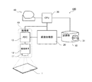
図1は、本発明の実施形態に係る欠陥検出装置100を説明する機能ブロック図である。
欠陥検出装置100は、被検査物1を撮像し、画像処理により被検査物1の欠陥を検出する装置であり、撮像部10、画像処理部20、CPU30、入出力端末40、記憶部50などを含み構成されている。
(Embodiment)
FIG. 1 is a functional block diagram illustrating a
The
被検査物1は、平板状製造物であり、例えば半導体デバイスや表示パネルなどがある。
撮像部10は、光学系11、撮像素子12、ADC回路13などから構成され、CPU30の制御のもとに被検査物1を撮像し、撮像画像(以下第1検査画像)を画像処理部20に送る。第1検査画像は、撮像素子12が捉えたマトリクス状の画素情報であり、画素毎の例えば輝度情報などの画素データから構成される。
画像処理部20は、CPU30の制御のもとに、後述する欠陥検出方法に従い第1検査画像を処理することにより被検査物1の欠陥を検出する。
ここで言う欠陥とは、平板状製造物において、その表面に現れた意図しない生成状態を呈する部分を言う。具体的には、例えば、シリコンウェーハー上にPZT(チタン酸ジルコン酸鉛)などを薄膜成形したもの(プリンタヘッド前工程のウェーハー)の表面のエッチング異常や、PZT単体の表面の傷、異物、樹脂フィルム表面やガラス表面、配線などの金属めっき表面の傷、異物、薄膜貼り合わせ時の異物挟み込みによる形状異常などである。
CPU30は、欠陥検出装置100の全体を司るCPU(Central Processing Unit)である。
入出力端末40は、欠陥検出装置100の稼動制御、検査結果の表示などを行うインターフェイス端末である。
記憶部50は、画像処理部20によって処理された画像情報や欠陥検出プログラム31などを格納する記憶装置である。
欠陥検出プログラム31は、CPU30により実行されるプログラムであり、以下に説明する欠陥検出方法に従い欠陥検出装置100を動作させる。
The object to be inspected 1 is a flat product, such as a semiconductor device or a display panel.
The
The
The defect said here refers to the part which exhibits the unintended production | generation state which appeared on the surface in a flat product. Specifically, for example, etching abnormalities on the surface of a silicon wafer formed with PZT (lead zirconate titanate) thin film (wafer in front of the printer head), scratches on the surface of the PZT alone, foreign matter, resin Examples include scratches on the surface of the metal plating such as the film surface, glass surface, and wiring, foreign matter, and shape abnormalities due to foreign matter pinching when the thin film is bonded.
The
The input /
The
The
(欠陥検出方法)
図2は、欠陥検出装置100を用いて被検査物1の欠陥を検出する方法を示すフローチャートである。また、図3(a),(b)は、欠陥を検出する際に必要な基準画像を作成する画像処理の方法を説明するグラフである。図1,図2、および図3(a),(b)を参照して欠陥検出方法を説明する。
(Defect detection method)
FIG. 2 is a flowchart showing a method for detecting a defect in the
まず、被検査物1を撮像部10の撮像視野にセットする(ステップS1)。
次に、被検査物1を撮像して被検査物1の第1検査画像を取得し(ステップS2)、第1検査画像を記憶部50に格納する(ステップS3)。
First, the
Next, the
次に、画像処理部20において、第1検査画像を複数の第1領域に分割する(ステップS4)。具体的には、複数の画素から構成される第1検査画像を、複数の第1領域としての隣り合う小集団の画素グループに分割する。第1領域としては、例えば、一次元に配列されるグループとして、第1検査画像を構成する複数の画素行、あるいは画素行と交差する複数の画素列をそれぞれ分割して得られる画素グループであればよい。また、例えば、二次元に配列されるグループとして、隣り合う複数の分割された画素列、あるいは隣り合う複数の分割された画素行の画素からなる画素グループであればよい。なお、分割された複数の第1領域のそれぞれに属する画素の数は同一であることが望ましい。つまり同じ画素数で分割することが望ましい。
次に、それぞれの第1領域に含まれる画素が持つ画素データの平均値(以下平均値A)を算出する(ステップS5)。
Next, the
Next, an average value (hereinafter, average value A) of pixel data of pixels included in each first region is calculated (step S5).
なお、分割する数(つまりは、分割した結果としての第1領域の大きさ)は、第1検査画像に周期性パターンが含まれる場合には、その周期(周期幅)、また検出すべき欠陥の大きさなどにより適宜設定する。例えば、画像むらが周期性の分布を示す場合には、第1領域の大きさは、その周期の4分の1以下であることが好ましく、また、周期の6分の1以下であることがより好ましい。
ここで、画像に周期性パターンが含まれる場合とは、第1検査画像における画素データの値が連続的に変化する起伏がある場合で、その起伏に周期性が認められる場合を言う。また、周期性が認められるとは、起伏の頂点の間隔を比較した場合に10倍以上の差異が無い場合を言う。
Note that the number of divisions (that is, the size of the first area as a result of division) is the period (period width) when the first inspection image includes a periodic pattern, and the defect to be detected. Set appropriately depending on the size of the. For example, when the image unevenness shows a distribution of periodicity, the size of the first region is preferably equal to or less than ¼ of the period, and may be equal to or less than one sixth of the period. More preferred.
Here, the case where the image includes a periodic pattern refers to a case where there is an undulation in which the value of the pixel data in the first inspection image continuously changes, and the undulation has a periodicity. In addition, the term “periodicity is recognized” refers to a case where there is no difference of 10 times or more when the intervals between the undulation vertices are compared.
次に、画像処理部20において、第1検査画像を構成する画素の画素データを、それぞれの第1領域の平均値Aを補間するデータに置き換えることで基準画像を作る(ステップS6)。具体的には、それぞれの第1領域の特定位置の画素データをその第1領域の平均値Aとし、この特定位置の画素に隣接する画素の画素データを、隣接する第1領域の特定位置の平均値Aを持つ画素データどうしを結ぶ補間データに置き換える。例えば、図3(a)に示すように、第1領域がそれぞれ3つの画素からなる領域s1〜s5の場合には、それぞれの領域の平均値Aは、平均値A1〜A5となる。また、補間データへの置き換えは、図3(b)に示すように、それぞれの第1領域の特定位置(この場合は、中央の画素)の画素データを平均値A1〜A5に置き換え、それぞれの平均値A1〜A5を直線で結び、それぞれの第1領域の中央の画素の両隣りの画素の画素データを直線に交差する値とすることにより行う。
このように、それぞれの第1領域の平均値Aを補間するデータに置き換えることで基準画像を作り、基準画像を記憶部50に格納する(ステップS7)。
なお、それぞれの平均値Aを結ぶことによる補間は、上記のような直線によるもの(直線近似)に限定するものではなく、2次曲線などで結ぶ曲線近似や、空間で捉えた場合には、曲面で結ぶ方法であっても良い。
Next, the
In this way, a reference image is created by replacing the average value A of each first region with the data to be interpolated, and the reference image is stored in the storage unit 50 (step S7).
In addition, the interpolation by connecting the respective average values A is not limited to the above-described straight line (straight line approximation). A method of connecting with a curved surface may be used.
次に、画像処理部20において、格納しておいた第1検査画像の画像データから基準画像の画像データを差し引いて第2検査画像を生成する(ステップS8)。具体的には、第1検査画像と基準画像それぞれの対応する画素どうしの画素データの演算(引き算)結果を持つ第2検査画像を生成する。その結果を記憶部50に格納する(ステップS9)。
Next, the
基準画像の画像データは、分割した領域(第1領域)の平均値Aおよび補間データで構成されている。つまり、いずれかの第1領域内に欠陥データが含まれている場合であっても、領域内で平均化されることで突出した欠陥データはレベリングされる。また、画像むらに周期性がある場合には、第1領域の大きさを、周期の4分の1以下ないしは6分の1以下としている。これは、画像むらを含んでレベリングされることを避けるためである。例えば、画像むらと同一の周期幅で平均化すると平均値Aは、略一定の値となってしまい複数の第1領域に亘る画像むらが反映された画像データとして基準画像を得ることができなくなる。
つまり、基準画像は、欠陥データがレベリングされ、画像むらが反映された画像データとして作成される。従って、第1検査画像の画像データから基準画像の画像データを差し引くことで、欠陥データを際立たせることが可能となる。
The image data of the reference image is composed of the average value A of the divided area (first area) and interpolation data. That is, even if defect data is included in any of the first regions, the defect data that protrudes by averaging in the region is leveled. In addition, when the image unevenness has periodicity, the size of the first region is set to ¼ or less or 6 or less of the cycle. This is to avoid leveling including image unevenness. For example, when averaging with the same period width as the image unevenness, the average value A becomes a substantially constant value, and it becomes impossible to obtain a reference image as image data reflecting image unevenness over a plurality of first regions. .
That is, the reference image is created as image data in which defect data is leveled and image unevenness is reflected. Therefore, it is possible to make the defect data stand out by subtracting the image data of the reference image from the image data of the first inspection image.
次に、画像処理部20において、第2検査画像を複数の第2領域に分割する(ステップS10)。具体的には、複数の画素から構成される第2検査画像を、複数の第2領域としての隣り合う小集団の画素グループに分割する。第2領域としては、例えば、一次元に配列されるグループとして、第2検査画像を構成する複数の画素列、あるいは画素列と交差する複数の画素行をそれぞれ分割して得られる画素グループであればよい。また、例えば、二次元に配列されるグループとして、隣り合う複数の分割された画素列、あるいは隣り合う複数の分割された画素行の画素からなる画素グループであればよい。なお、分割する数(第2領域の大きさ)は、検出すべき欠陥の大きさなどにより適宜設定する。なお、分割された複数の第2領域のそれぞれに属する画素の数は同一であることが望ましい。つまり同じ画素数で分割することが望ましい。
次に、それぞれの第2領域に含まれる画素が持つ画素データの平均値(以下平均値B)を算出して比較画像を生成し(ステップS11)、記憶部50に格納する(ステップS12)。
Next, the
Next, an average value (hereinafter, average value B) of pixel data of pixels included in each second region is calculated to generate a comparative image (step S11), and is stored in the storage unit 50 (step S12).
次に、画像処理部20において、格納しておいた第2検査画像の画像データから比較画像の画像データを差し引いて判定画像を生成する(ステップS13)。具体的には、第2検査画像と比較画像それぞれの対応する画素どうしの画素データの演算(引き算)結果を持つ判定画像を生成する。
次に、判定画像に対し所定の閾値をもって判定し、欠陥の検出を行う(ステップS14)。具体的には、判定画像を構成するそれぞれの画素の画素データと所定の閾値とを比較して画素毎に判定を行う。
次に、欠陥検出結果の出力をする(ステップS15)。具体的には、判定画像に対して検出した欠陥位置を示す画素を識別表示した画像を生成し入出力端末40などに表示し、欠陥検出を完了する。
Next, the
Next, it determines with a predetermined threshold with respect to a determination image, and detects a defect (step S14). Specifically, the determination is performed for each pixel by comparing pixel data of each pixel constituting the determination image with a predetermined threshold value.
Next, a defect detection result is output (step S15). Specifically, an image in which pixels indicating the defect position detected with respect to the determination image are identified and generated is generated and displayed on the input /
(実施例)
上述した方法に従って実施した例について以下に説明する。
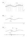
図4(a)は、実施例における被検査物1を模式的に示す平面図、図4(b)は、第1検査画像を構成する画素の輝度分布の例を示すグラフである。
図4(a)に示す被検査物1は、矩形平板であり、表面には許容できる画像むら4と、検出すべき欠陥3がある例を示している。被検査物1を撮像して得られた第1検査画像は、図4(a)に示すX方向の行と、X方向に交差するY方向の列とでマトリクス状に並ぶ画素データ(輝度分布)から構成される。図4(b)に示すグラフは、図4(a)に1点鎖線で示す位置に対応する画素行の輝度分布を示しており、欠陥3に対応する位置(D1部)の輝度が低下している様子を示している。また、画像むら4は、図4(b)に示すように輝度が周期的に低下している。画像むら4の中央部分の距離(u1、u2)は、画像むら4の周期幅を示すものである。u1とu2の距離は略同じである。
(Example)
An example implemented according to the method described above will be described below.
FIG. 4A is a plan view schematically showing the
The
本実施例では、第1領域として、第1検査画像を構成する画素行を分割して得られる画素グループ(一次元に配列される画素グループ)を用いている。また、欠陥を検出するための画像処理は、画素行毎に行っている。
図5は、本実施例における具体的な欠陥検出方法を示すフローチャートである。
図5を参照して本実施例の欠陥検出方法を説明する。
In the present embodiment, a pixel group (pixel group arranged one-dimensionally) obtained by dividing a pixel row constituting the first inspection image is used as the first region. Further, image processing for detecting a defect is performed for each pixel row.
FIG. 5 is a flowchart showing a specific defect detection method in this embodiment.
The defect detection method of the present embodiment will be described with reference to FIG.
まず、被検査物1を撮像部10の撮像視野にセットする(ステップSA1)。
次に、被検査物1を撮像して被検査物1の第1検査画像を取得し、第1検査画像を記憶部50に格納する(ステップSA2)。
次に、欠陥の検出を行う画素行をセットする。初期位置はn=1とする(ステップSA3)。nには、最終行の値まで順にセットされる。
次に、格納した第1検査画像から、第n行の画素データを抽出する(ステップSA4)。
次に、第n行の検査(欠陥の検出)を行い(ステップSA5)、検査結果を記憶部50に格納する(ステップSA6)。
ステップSA5の画素行毎の検査(欠陥検出)の方法を示すサブルーチンについては、後述する。
First, the
Next, the
Next, a pixel row for detecting a defect is set. The initial position is n = 1 (step SA3). n is sequentially set up to the value of the last row.
Next, pixel data of the nth row is extracted from the stored first inspection image (step SA4).
Next, the n-th row inspection (defect detection) is performed (step SA5), and the inspection result is stored in the storage unit 50 (step SA6).
A subroutine showing the inspection (defect detection) method for each pixel row in step SA5 will be described later.
次に、第n行の検査結果の良否を認識する(ステップSA7)。具体的には、ステップSA5において所定の閾値を越える欠陥が検出されなかった場合は、Passと認識し、検出された場合はFailと認識する。
Passと認識された場合は、検査が完了しているかを確認する(ステップSA9)。具体的には、nの値が所定の最終行の値に達したかを確認する。
ステップSA7にて、Failと認識された場合には、検査を継続するか確認する(ステップSA8)。具体的には、欠陥が検出されたタイミングで被検査物1の検査を終了するモード(フェイルストップモード)などに予め設定されていた場合には、検査を完了し、検査結果の出力する(ステップSA10)。検査を継続する場合には、検査が完了しているかを確認する(ステップSA9)。
ステップSA9にて、検査が完了していないと認識された場合、具体的には、nの値が所定の最終行の値に達していない場合には、nの値をインクリメントして(ステップSA11)、次の第n行の画素を抽出し(ステップSA4)、以降ステップSA5以降を繰り返す。
ステップSA9にて、検査が完了したと認識された場合、具体的には、nの値が所定の最終行の値に達した場合には、検査結果の出力をし(ステップSA10)、検査を完了する。具体的には、検出した欠陥位置を示す画素を識別表示した画像を生成し、入出力端末40などに表示し、欠陥検出を完了する。
Next, the quality of the inspection result in the nth row is recognized (step SA7). Specifically, when a defect exceeding a predetermined threshold is not detected in step SA5, it is recognized as Pass, and when it is detected, it is recognized as Fail.
If it is recognized as Pass, it is confirmed whether the inspection is completed (step SA9). Specifically, it is confirmed whether the value of n has reached the value of a predetermined last row.
If it is recognized as Fail in step SA7, it is confirmed whether or not the inspection is continued (step SA8). Specifically, when a mode for ending the inspection of the
When it is recognized in step SA9 that the inspection has not been completed, specifically, when the value of n has not reached the value of the predetermined final row, the value of n is incremented (step SA11). ), The pixel in the next n-th row is extracted (step SA4), and thereafter, steps SA5 and after are repeated.
When it is recognized in step SA9 that the inspection is completed, specifically, when the value of n reaches the value of the predetermined final row, the inspection result is output (step SA10), and the inspection is performed. Complete. Specifically, an image in which the pixel indicating the detected defect position is identified and displayed is generated and displayed on the input /
次に、図6〜図8を参照して、ステップSA5の画素行毎の検査方法(欠陥検出方法)について説明する。
図6は、ステップSA5の画素行毎の検査(欠陥検出)の方法を示すサブルーチン、つまり、一つの画素行における欠陥検出方法を示すフローチャートである。
図7(a)〜(c)、および図8(a)〜(c)は、画像処理部20によって処理される画像データ(輝度分布)を示すグラフである。
Next, an inspection method (defect detection method) for each pixel row in step SA5 will be described with reference to FIGS.
FIG. 6 is a flowchart showing a subroutine showing a method of inspection (defect detection) for each pixel row in step SA5, that is, a defect detection method in one pixel row.
FIGS. 7A to 7C and FIGS. 8A to 8C are graphs showing image data (luminance distribution) processed by the
ステップSA5は、第1検査画像から抽出された第n行の画素データを対象として検査(欠陥の検出)を行うステップである。以下の説明では、抽出された第n行の画素データとして、図4(a)に1点鎖線で示す位置に対応する画素行、つまり欠陥3を検出すべき画素行を例に説明する。以下、この画素行を図4(a)に示すように、画素行2と言う。
まず、抽出された画素行2の画素データ(以下データa)を記憶部50に格納する(ステップSB1)。図7(a)にデータaのグラフを示す。このグラフは、画素行2の輝度Lの分布を示すものである。
次に、画像処理部20において、画素行2の画素データを複数の第1領域に分割する(ステップSB2)。具体的には、図7(b)に示すように、連続する一行の画素を、破線部分で分割された複数の第1領域としての隣り合う小集団の画素グループに分割する。本実施例では、第1領域の幅を、画像むら4の周期の約6.5分の1としている。
次に、それぞれの第1領域に含まれる画素が持つ画素データ(輝度L)の平均値(以下平均値A)を算出する(ステップSB3)。
Step SA5 is a step in which inspection (defect detection) is performed on pixel data in the n-th row extracted from the first inspection image. In the following description, the pixel data corresponding to the position indicated by the one-dot chain line in FIG. 4A, that is, the pixel row where the
First, the extracted pixel data of pixel row 2 (hereinafter, data a) is stored in the storage unit 50 (step SB1). FIG. 7A shows a graph of data a. This graph shows the distribution of the luminance L of the
Next, the
Next, an average value (hereinafter referred to as average value A) of pixel data (luminance L) of pixels included in each first region is calculated (step SB3).
次に、画像処理部20において、データaを、それぞれの第1領域の平均値Aを補間するデータに置き換えることで基準画像としてのデータbを作る(ステップSB4)。具体的には、図8(a)に示すように、それぞれの第1領域の特定位置(本例では中央位置)の画素データをその第1領域の平均値Aとし、この特定位置の画素に隣接する画素の画素データを、隣接する第1領域の特定位置の平均値Aを持つ画素データどうしを結ぶ補間データに置き換える。補間データへの置き換えは、図8(a)に示すように、それぞれの第1領域の中央の画素の画素データをそれぞれの平均値Aに置き換え、それぞれの平均値Aを直線で結び、他の画素の画素データを直線上の値とすることにより行う。
このように、それぞれの第1領域の平均値Aを補間するデータに置き換えることでデータb(基準画像)を作り、データbを記憶部50に格納する(ステップSB5)。
なお、それぞれの平均値Aを結ぶ補間は、上記のような直線によるもの(直線近似)に限定するものではなく、2次曲線などで結ぶ方法(曲線近似)であっても良い。
Next, in the
In this way, the data b (reference image) is created by replacing the average value A of each first region with the data to be interpolated, and the data b is stored in the storage unit 50 (step SB5).
The interpolation connecting the respective average values A is not limited to the above-described straight line (linear approximation), and may be a method of connecting with a quadratic curve (curve approximation).
次に、画像処理部20において、格納しておいたデータa(第1検査画像の画像データ)からデータb(基準画像の画像データ)を差し引いてデータc(第2検査画像)を生成する(ステップSB6)。具体的には、データaとデータbそれぞれの対応する画素どうしの画素データの演算(引き算)結果を持つデータcを生成する。その結果を記憶部50に格納する(ステップSB7)。図8(b)にデータa,データbのグラフを示す。図8(c)にデータa,データcのグラフを示す。
Next, the
次に、画像処理部20において、データcを複数の第2領域に分割する(ステップSB8)。具体的には、連続する一行の画素を、分割された複数の第2領域としての隣り合う小集団の画素グループに分割する。本実施例では、第2領域の大きさは、第1領域と同じ大きさとなるように分割している(以下図示省略)。
次に、それぞれの第2領域に含まれる画素が持つ画素データの平均値(以下平均値B)を算出してデータd(比較画像)を生成し(ステップSB9)、記憶部50に格納する(ステップSB10)。
Next, the
Next, an average value (hereinafter referred to as average value B) of pixel data of pixels included in each second region is calculated to generate data d (comparison image) (step SB9), and is stored in the storage unit 50 ( Step SB10).
次に、画像処理部20において、格納しておいたデータcからデータdを差し引いて判定画像を生成する(ステップSB11)。具体的には、データcとデータdそれぞれの対応する画素どうしの画素データの演算(引き算)結果を持つ判定画像データを生成する。
次に、画像処理部20は、判定画像データに対し所定の閾値をもって判定し、欠陥の検出を行う(ステップSB12)。具体的には、判定画像を構成するそれぞれの画素の画素データと所定の閾値とを比較して画素毎に判定を行う。以上により、第n行の画素データを対象とした検査(欠陥の検出)を完了する。
Next, the
Next, the
図9は、被検査物1を撮像して得られた画像データ(第1検査画像としてのデータa)と、本実施例の方法により得られた判定画像データとを比較して示すグラフである。
第1検査画像では、データaに対して欠陥3に対応するD1部を検出する閾値L1が設定できないが、判定画像では、判定画像データに対して欠陥3に対応するD2部を検出する閾値L2の設定が可能となっている。
FIG. 9 is a graph showing comparison between image data obtained by imaging the inspection object 1 (data a as the first inspection image) and determination image data obtained by the method of the present embodiment. .
In the first inspection image, the threshold value L1 for detecting the D1 portion corresponding to the
以上述べたように、本実施形態による欠陥検出装置100、および欠陥検出方法によれば、以下の効果を得ることができる。
撮像部10は、被検査物1を撮像して被検査物1の第1検査画像を取得する。被検査物1に検出すべき欠陥3がある場合には、欠陥3を反映した画像データを有する第1検査画像が得られる。これに対して、画像処理部20は、まず、第1検査画像を複数の第1領域に分割し、それぞれの第1領域に含まれる画素が持つ画素データの平均値Aを算出し、それぞれの画素の画素データを、それぞれの第1領域の平均値Aを補間するデータに置き換えることで基準画像を作る。つまり、いずれかの第1領域内に欠陥データが含まれている場合であっても、平均化されることで欠陥データがレベリングされ、複数の第1領域に亘る画像むら4が反映された画像データとして基準画像が得られる。次に、画像処理部20は、第1検査画像の画素データから基準画像の画素データを減算して、第2検査画像を作る。つまり、第1検査画像から画像むら4の影響が取り除かれた、あるいは軽減された画像データとして第2検査画像が得られる。
具体的には、実施例の場合には、図8(b),(c)に示すように、第1検査画像としてのデータaから画像むら4が反映されたデータbを減算して、画像むら4の影響が取り除かれた、あるいは軽減されたデータcが作られる。
As described above, according to the
The
Specifically, in the case of the embodiment, as shown in FIGS. 8B and 8C, the data b reflecting the
次に、画像処理部20は、第2検査画像を複数の第2領域に分割し、それぞれの第2領域に含まれる画素が持つ画素データの平均値Bを算出し、それぞれの第2領域に含まれる画素の画素データを平均値Bに置き換えることで比較画像を作る。つまり、いずれかの第2領域内に欠陥データが含まれている場合であっても、平均化されることでレベリングされた画像データとして比較画像が得られる。次に、画像処理部20は、第2検査画像と比較画像との画素データの差分を計算する。
具体的には、実施例の場合には、データcを複数の第2領域に分割し、それぞれの第2領域に含まれる画素が持つ画素データの平均値Bを算出し、それぞれの第2領域に含まれる画素の画素データを平均値Bに置き換えることでデータdを作る。次に、画像処理部20は、データcとデータdとの画素データの差分を計算する。
つまり、例えば、第2検査画像(データc)に画像むら4による影響が残っている場合であっても、比較画像(データd)との画素データの差分を計算することで、画像むら4による影響をより多く取り除くことができ、欠陥データが含まれている場合には、欠陥データが抽出される。
Next, the
Specifically, in the case of the embodiment, the data c is divided into a plurality of second areas, the average value B of the pixel data of the pixels included in each second area is calculated, and each second area is calculated. The data d is created by replacing the pixel data of the pixels included in the data with the average value B. Next, the
That is, for example, even when the influence of the
以上のように本実施形態による欠陥検出装置100、および欠陥検出方法によれば、欠陥3による画像データの値の変動が画像むら4のレンジ(画像むら4による画像データの差幅)と同程度以下の場合であっても、画像むら4による画像データの影響を取り除く、あるいは軽減することが可能であり、欠陥部分に対応する画像データが抽出されるため、欠陥を検出するための閾値の幅(値)を、画像むらの幅(値)よりも小さい範囲に設定することができる。その結果、より欠陥の検出感度が高い欠陥検出装置を提供することができる。
As described above, according to the
なお、上記の説明では、欠陥を検出する画素データを輝度として説明したが、これに限定するものではなく、被検査物1の欠陥が反映される画像データであれば良い。例えば、彩度や色相など、撮像素子によって数値化できるデータであれば良い。
また、被検査物1は、平板状製造物であり、例えば半導体デバイスや表示パネルなどがあると説明したが、被検査物1の対象としては、これらに限定するものではなく、略均一な状態の表面に撮像素子によって識別され数値化できる欠陥が含まれるものや、表面が均一ではなくとも、所定のパターンをマスキングすることによって均一な表面と欠陥による異常状態とに識別され数値化できるものが適用できる。具体的には、例えば、シリコンウェーハー上にPZT(チタン酸ジルコン酸鉛)などを薄膜成形したもの(プリンタヘッド前工程のウェーハー)の表面のエッチング異常の検出や、PZT単体の表面の傷、異物の検出、樹脂フィルム表面やガラス表面、配線などの金属めっき表面の傷、異物の検出、薄膜貼り合わせ時の異物挟み込みによる形状異常などの検出にも適用できる。
In the above description, the pixel data for detecting the defect is described as the luminance. However, the present invention is not limited to this, and any image data that reflects the defect of the
Moreover, although the inspected
(欠陥検出プログラム)
図1に戻り、欠陥検出プログラムについて説明する。
本実施形態における欠陥検出プログラムとしての欠陥検出プログラム31は、欠陥検出装置100を動作させるプログラムであり、記憶部50に格納されている。欠陥検出装置100を動作させるにあたり、入出力端末40からの操作などにより起動し、画像処理部20におけるデータ処理としてCPU30により実行される。
具体的には、上述した欠陥検出方法の例におけるステップS2あるいはステップSA2などで取得された第1検査画像の画像データに対し、予め入出力端末40などからの入力で設定された所定の閾値や、所定の検査モードなどを参照して、例えば、ステップS3からステップS15、あるいはステップSA3からステップSA11などを含む処理を行う。
(Defect detection program)
Returning to FIG. 1, the defect detection program will be described.
A
Specifically, for the image data of the first inspection image acquired in step S2 or step SA2 in the example of the defect detection method described above, a predetermined threshold value set in advance by input from the input /
欠陥検出プログラム31によれば、欠陥検出装置100において、上述した欠陥検出方法に従い被検査物1の欠陥検出を行うことで、欠陥3による画像データの値の変動が画像むら4のレンジ(画像むら4による画像データの差幅)と同程度以下の場合であっても、画像むら4による画像データの影響を取り除く、あるいは軽減することが可能であり、欠陥部分に対応する画像データが抽出されるため、欠陥を検出するための閾値の幅(値)を、画像むらの幅(値)よりも小さい範囲に設定することができる。その結果、より欠陥の検出感度が高い欠陥検出装置を提供することができる。
According to the
1…被検査物、3…欠陥、10…撮像部、11…光学系、12…撮像素子、13…ADC回路、20…画像処理部、30…CPU、31…欠陥検出プログラム、40…入出力端末、50…記憶部、100…欠陥検出装置。
DESCRIPTION OF
Claims (10)
前記撮像部が取得した前記第1検査画像を処理する画像処理部と、を備え、
前記画像処理部は、
前記第1検査画像を複数の第1領域に分割し、それぞれの前記第1領域に含まれる画素が持つ画素データの平均値Aと前記平均値Aを補間するデータとを算出し、前記平均値Aと前記平均値Aを補間するデータとから基準画像を作り、
前記第1検査画像の画素データから前記基準画像の画素データを減算して、第2検査画像を作り、
前記第2検査画像を複数の第2領域に分割し、それぞれの前記第2領域に含まれる画素が持つ画素データの平均値Bを算出し、前記平均値Bから比較画像を作り、
前記第2検査画像と前記比較画像との画素データの差分を計算し、前記差分が所定の閾値以上となる画素データに対応する位置を欠陥として検出することを特徴とする欠陥検出装置。 An imaging unit that images the inspection object and obtains a first inspection image of the inspection object;
An image processing unit that processes the first inspection image acquired by the imaging unit,
The image processing unit
Dividing the first inspection image into a plurality of first areas, calculating an average value A of pixel data of pixels included in each of the first areas and data interpolating the average value A, and calculating the average value A reference image is created from A and data for interpolating the average value A,
Subtracting the pixel data of the reference image from the pixel data of the first inspection image to create a second inspection image,
Dividing the second inspection image into a plurality of second regions, calculating an average value B of pixel data of pixels included in each of the second regions, and making a comparison image from the average value B;
A defect detection apparatus, wherein a difference between pixel data between the second inspection image and the comparison image is calculated, and a position corresponding to pixel data where the difference is equal to or greater than a predetermined threshold is detected as a defect.
前記第1領域は、前記周期性パターンの周期の4分の1以下であることを特徴とする請求項1に記載の欠陥検出装置。 When a periodic pattern is included in the first inspection image,
The defect detection apparatus according to claim 1, wherein the first region is equal to or less than a quarter of a period of the periodic pattern.
前記第1領域は、前記周期性パターンの周期の6分の1以下であることを特徴とする請求項1に記載の欠陥検出装置。 When a periodic pattern is included in the first inspection image,
The defect detection apparatus according to claim 1, wherein the first region is 1/6 or less of a period of the periodic pattern.
前記第1検査画像を複数の第1領域に分割し、それぞれの前記第1領域に含まれる画素が持つ画素データの平均値Aと前記平均値Aを補間するデータとを算出し、前記平均値Aと前記平均値Aを補間するデータとから基準画像を作るステップと、
前記第1検査画像の画素データから前記基準画像の画素データを減算して、第2検査画像を作るステップと、
前記第2検査画像を複数の第2領域に分割し、それぞれの前記第2領域に含まれる画素が持つ画素データの平均値Bを算出し、前記平均値Bから比較画像を作るステップと、
前記第2検査画像と前記比較画像との画素データの差分を計算し、前記差分が所定値以上となる画素データに対応する位置を欠陥として検出するステップと、を含むことを特徴とする欠陥検出方法。 Capturing a first inspection image of the inspection object by imaging the inspection object;
Dividing the first inspection image into a plurality of first areas, calculating an average value A of pixel data of pixels included in each of the first areas and data interpolating the average value A, and calculating the average value Creating a reference image from A and data interpolating the average value A;
Subtracting pixel data of the reference image from pixel data of the first inspection image to create a second inspection image;
Dividing the second inspection image into a plurality of second regions, calculating an average value B of pixel data of pixels included in each of the second regions, and creating a comparison image from the average value B;
Calculating a difference in pixel data between the second inspection image and the comparison image, and detecting a position corresponding to the pixel data in which the difference is equal to or greater than a predetermined value as a defect. Method.
前記被検査物を撮像して得られた第1検査画像を処理することで欠陥を検出するプログラムであって、
前記第1検査画像を複数の第1領域に分割し、それぞれの前記第1領域に含まれる画素が持つ画素データの平均値Aと前記平均値Aを補間するデータとを算出し、前記平均値Aと前記平均値Aを補間するデータとから基準画像を作るステップと、
前記第1検査画像の画素データから前記基準画像の画素データを減算して、第2検査画像を作るステップと、
前記第2検査画像を複数の第2領域に分割し、それぞれの前記第2領域に含まれる画素が持つ画素データの平均値Bを算出し、前記平均値Bから比較画像を作るステップと、
前記第2検査画像と前記比較画像との画素データの差分を計算し、前記差分が所定値以上となる画素データに対応する位置を欠陥として検出するステップと、を含むことを特徴とする欠陥検出プログラム。 It is executed by a defect detection device that detects defects in the inspection object,
A program for detecting a defect by processing a first inspection image obtained by imaging the inspection object,
Dividing the first inspection image into a plurality of first areas, calculating an average value A of pixel data of pixels included in each of the first areas and data interpolating the average value A, and calculating the average value Creating a reference image from A and data interpolating the average value A;
Subtracting pixel data of the reference image from pixel data of the first inspection image to create a second inspection image;
Dividing the second inspection image into a plurality of second regions, calculating an average value B of pixel data of pixels included in each of the second regions, and creating a comparison image from the average value B;
Calculating a difference in pixel data between the second inspection image and the comparison image, and detecting a position corresponding to the pixel data in which the difference is equal to or greater than a predetermined value as a defect. program.
Priority Applications (1)
| Application Number | Priority Date | Filing Date | Title |
|---|---|---|---|
| JP2012125889A JP2013250188A (en) | 2012-06-01 | 2012-06-01 | Defect detection device, defect detection method and defect detection program |
Applications Claiming Priority (1)
| Application Number | Priority Date | Filing Date | Title |
|---|---|---|---|
| JP2012125889A JP2013250188A (en) | 2012-06-01 | 2012-06-01 | Defect detection device, defect detection method and defect detection program |
Publications (2)
| Publication Number | Publication Date |
|---|---|
| JP2013250188A true JP2013250188A (en) | 2013-12-12 |
| JP2013250188A5 JP2013250188A5 (en) | 2015-06-18 |
Family
ID=49849007
Family Applications (1)
| Application Number | Title | Priority Date | Filing Date |
|---|---|---|---|
| JP2012125889A Withdrawn JP2013250188A (en) | 2012-06-01 | 2012-06-01 | Defect detection device, defect detection method and defect detection program |
Country Status (1)
| Country | Link |
|---|---|
| JP (1) | JP2013250188A (en) |
Cited By (5)
| Publication number | Priority date | Publication date | Assignee | Title |
|---|---|---|---|---|
| JP2015169564A (en) * | 2014-03-07 | 2015-09-28 | 株式会社ダイヘン | Image inspection device and image inspection method |
| US9429779B2 (en) | 2014-08-19 | 2016-08-30 | Samsung Electronics Co., Ltd. | Electro-optic modulator including composite materials and testing apparatus including the same |
| CN109900707A (en) * | 2019-03-20 | 2019-06-18 | 湖南华曙高科技有限责任公司 | A kind of powdering quality detection method, equipment and readable storage medium storing program for executing |
| KR20220094593A (en) * | 2020-12-29 | 2022-07-06 | 부산대학교 산학협력단 | Apparatus and method for storing image data for surface defect detection scanner |
| CN116973311A (en) * | 2023-09-22 | 2023-10-31 | 成都中嘉微视科技有限公司 | Detection device and detection method for foreign matters on film and under film |
Citations (5)
| Publication number | Priority date | Publication date | Assignee | Title |
|---|---|---|---|---|
| JPH09145638A (en) * | 1995-11-24 | 1997-06-06 | Kawasaki Steel Corp | Method and device for detecting surface defect |
| JP2000329699A (en) * | 1999-05-20 | 2000-11-30 | Kobe Steel Ltd | Method and apparatus for inspection of defect |
| JP2008004085A (en) * | 2006-05-23 | 2008-01-10 | Matsushita Electric Ind Co Ltd | Image processing device, image processing method, program, recording medium and integrated circuit |
| JP2008070242A (en) * | 2006-09-14 | 2008-03-27 | Seiko Epson Corp | Noise-removing method and apparatus, unevenness defect inspecting method and apparatus |
| JP2009216475A (en) * | 2008-03-08 | 2009-09-24 | Kanto Auto Works Ltd | Surface inspection system and surface inspection method using the same |
-
2012
- 2012-06-01 JP JP2012125889A patent/JP2013250188A/en not_active Withdrawn
Patent Citations (5)
| Publication number | Priority date | Publication date | Assignee | Title |
|---|---|---|---|---|
| JPH09145638A (en) * | 1995-11-24 | 1997-06-06 | Kawasaki Steel Corp | Method and device for detecting surface defect |
| JP2000329699A (en) * | 1999-05-20 | 2000-11-30 | Kobe Steel Ltd | Method and apparatus for inspection of defect |
| JP2008004085A (en) * | 2006-05-23 | 2008-01-10 | Matsushita Electric Ind Co Ltd | Image processing device, image processing method, program, recording medium and integrated circuit |
| JP2008070242A (en) * | 2006-09-14 | 2008-03-27 | Seiko Epson Corp | Noise-removing method and apparatus, unevenness defect inspecting method and apparatus |
| JP2009216475A (en) * | 2008-03-08 | 2009-09-24 | Kanto Auto Works Ltd | Surface inspection system and surface inspection method using the same |
Cited By (9)
| Publication number | Priority date | Publication date | Assignee | Title |
|---|---|---|---|---|
| JP2015169564A (en) * | 2014-03-07 | 2015-09-28 | 株式会社ダイヘン | Image inspection device and image inspection method |
| US9429779B2 (en) | 2014-08-19 | 2016-08-30 | Samsung Electronics Co., Ltd. | Electro-optic modulator including composite materials and testing apparatus including the same |
| CN109900707A (en) * | 2019-03-20 | 2019-06-18 | 湖南华曙高科技有限责任公司 | A kind of powdering quality detection method, equipment and readable storage medium storing program for executing |
| CN109900707B (en) * | 2019-03-20 | 2021-07-02 | 湖南华曙高科技有限责任公司 | Powder paving quality detection method and device and readable storage medium |
| KR20220094593A (en) * | 2020-12-29 | 2022-07-06 | 부산대학교 산학협력단 | Apparatus and method for storing image data for surface defect detection scanner |
| KR102595278B1 (en) * | 2020-12-29 | 2023-10-27 | 부산대학교 산학협력단 | Apparatus and method for storing image data for surface defect detection scanner |
| US11961217B2 (en) | 2020-12-29 | 2024-04-16 | Pusan National University Industry—University Cooperation Foundation | Device and method for storing image data for surface defect detection scanner |
| CN116973311A (en) * | 2023-09-22 | 2023-10-31 | 成都中嘉微视科技有限公司 | Detection device and detection method for foreign matters on film and under film |
| CN116973311B (en) * | 2023-09-22 | 2023-12-12 | 成都中嘉微视科技有限公司 | Detection device and detection method for foreign matters on film and under film |
Similar Documents
| Publication | Publication Date | Title |
|---|---|---|
| JP2013250188A (en) | Defect detection device, defect detection method and defect detection program | |
| KR102301437B1 (en) | Vision inspection apparatus and method of detecting mura thereof | |
| TWI614721B (en) | Detection of defects embedded in noise for inspection in semiconductor manufacturing | |
| KR100846633B1 (en) | Method and apparatus for detecting defects of patterns | |
| JP4652391B2 (en) | Pattern inspection apparatus and pattern inspection method | |
| TWI605529B (en) | A system, a method and a computer program product for cad-based registration | |
| JP2006200972A (en) | Image defect inspection method, image defect inspection device, and external appearance inspection device | |
| JP2007147587A (en) | Surface distortion measuring device and method | |
| JP2010032403A (en) | Circuit pattern examining apparatus and circuit pattern examining method | |
| JP2008051617A (en) | Image inspection device, image inspection method and recording medium | |
| JP2019158351A (en) | Object recognition method, height measurement method, and three-dimensional measurement method | |
| US20150036915A1 (en) | Inspection Method | |
| JP4244046B2 (en) | Image processing method and image processing apparatus | |
| JP2006138708A (en) | Image flaw inspection method, image flaw inspecting device and visual inspection device | |
| KR101702752B1 (en) | Method of inspecting electronic components | |
| JPWO2008105463A1 (en) | Manufacturing method of inspection device | |
| JP2007057705A (en) | Inspection method and inspection apparatus of display panel | |
| US20100027871A1 (en) | Method and system for inspection of tube width of heat exchanger | |
| JP2006270334A (en) | Shading correction method and image inspection device | |
| JP5417997B2 (en) | Imaging inspection method | |
| JP6410459B2 (en) | Image inspection method and image inspection apparatus | |
| CN110062151B (en) | Smooth image generation device, abnormality determination device, and smooth image generation method | |
| JP2004333386A (en) | Reticle inspection apparatus and reticle inspection method | |
| JP2004037136A (en) | Apparatus and method for inspecting pattern | |
| JP2007104296A (en) | Method, apparatus, and program for measuring resolution |
Legal Events
| Date | Code | Title | Description |
|---|---|---|---|
| RD04 | Notification of resignation of power of attorney |
Free format text: JAPANESE INTERMEDIATE CODE: A7424 Effective date: 20150108 |
|
| A521 | Written amendment |
Free format text: JAPANESE INTERMEDIATE CODE: A523 Effective date: 20150428 |
|
| A621 | Written request for application examination |
Free format text: JAPANESE INTERMEDIATE CODE: A621 Effective date: 20150428 |
|
| A977 | Report on retrieval |
Free format text: JAPANESE INTERMEDIATE CODE: A971007 Effective date: 20160210 |
|
| A131 | Notification of reasons for refusal |
Free format text: JAPANESE INTERMEDIATE CODE: A131 Effective date: 20160223 |
|
| A761 | Written withdrawal of application |
Free format text: JAPANESE INTERMEDIATE CODE: A761 Effective date: 20160316 |