JP2013234977A - Sample analysis element, inspection device, and sensor cartridge - Google Patents
Sample analysis element, inspection device, and sensor cartridge Download PDFInfo
- Publication number
- JP2013234977A JP2013234977A JP2012109188A JP2012109188A JP2013234977A JP 2013234977 A JP2013234977 A JP 2013234977A JP 2012109188 A JP2012109188 A JP 2012109188A JP 2012109188 A JP2012109188 A JP 2012109188A JP 2013234977 A JP2013234977 A JP 2013234977A
- Authority
- JP
- Japan
- Prior art keywords
- nanostructure
- nanostructures
- sample analysis
- pitch
- analysis element
- Prior art date
- Legal status (The legal status is an assumption and is not a legal conclusion. Google has not performed a legal analysis and makes no representation as to the accuracy of the status listed.)
- Withdrawn
Links
Images


Classifications
-
- G—PHYSICS
- G01—MEASURING; TESTING
- G01N—INVESTIGATING OR ANALYSING MATERIALS BY DETERMINING THEIR CHEMICAL OR PHYSICAL PROPERTIES
- G01N21/00—Investigating or analysing materials by the use of optical means, i.e. using sub-millimetre waves, infrared, visible or ultraviolet light
- G01N21/62—Systems in which the material investigated is excited whereby it emits light or causes a change in wavelength of the incident light
- G01N21/63—Systems in which the material investigated is excited whereby it emits light or causes a change in wavelength of the incident light optically excited
- G01N21/65—Raman scattering
- G01N21/658—Raman scattering enhancement Raman, e.g. surface plasmons
-
- G—PHYSICS
- G01—MEASURING; TESTING
- G01N—INVESTIGATING OR ANALYSING MATERIALS BY DETERMINING THEIR CHEMICAL OR PHYSICAL PROPERTIES
- G01N21/00—Investigating or analysing materials by the use of optical means, i.e. using sub-millimetre waves, infrared, visible or ultraviolet light
- G01N21/62—Systems in which the material investigated is excited whereby it emits light or causes a change in wavelength of the incident light
- G01N21/63—Systems in which the material investigated is excited whereby it emits light or causes a change in wavelength of the incident light optically excited
- G01N21/65—Raman scattering
-
- B—PERFORMING OPERATIONS; TRANSPORTING
- B82—NANOTECHNOLOGY
- B82Y—SPECIFIC USES OR APPLICATIONS OF NANOSTRUCTURES; MEASUREMENT OR ANALYSIS OF NANOSTRUCTURES; MANUFACTURE OR TREATMENT OF NANOSTRUCTURES
- B82Y15/00—Nanotechnology for interacting, sensing or actuating, e.g. quantum dots as markers in protein assays or molecular motors
-
- G—PHYSICS
- G01—MEASURING; TESTING
- G01N—INVESTIGATING OR ANALYSING MATERIALS BY DETERMINING THEIR CHEMICAL OR PHYSICAL PROPERTIES
- G01N2201/00—Features of devices classified in G01N21/00
- G01N2201/06—Illumination; Optics
- G01N2201/061—Sources
- G01N2201/06113—Coherent sources; lasers
-
- Y—GENERAL TAGGING OF NEW TECHNOLOGICAL DEVELOPMENTS; GENERAL TAGGING OF CROSS-SECTIONAL TECHNOLOGIES SPANNING OVER SEVERAL SECTIONS OF THE IPC; TECHNICAL SUBJECTS COVERED BY FORMER USPC CROSS-REFERENCE ART COLLECTIONS [XRACs] AND DIGESTS
- Y10—TECHNICAL SUBJECTS COVERED BY FORMER USPC
- Y10S—TECHNICAL SUBJECTS COVERED BY FORMER USPC CROSS-REFERENCE ART COLLECTIONS [XRACs] AND DIGESTS
- Y10S977/00—Nanotechnology
- Y10S977/902—Specified use of nanostructure
- Y10S977/932—Specified use of nanostructure for electronic or optoelectronic application
- Y10S977/953—Detector using nanostructure
- Y10S977/954—Of radiant energy
Abstract
Description
本発明は、金属膜で覆われるナノ体を備える試料分析素子、および、そういった試料分析素子を利用した検査装置およびセンサーカートリッジ等に関する。 The present invention relates to a sample analysis element including a nanobody covered with a metal film, and an inspection apparatus and a sensor cartridge using such a sample analysis element.
局在表面プラズモン共鳴(LSPR)を利用した試料分析素子は知られる。こうした試料分析素子は例えば金属膜で覆われるナノ体を備える。ナノ体は例えば励起光の波長よりも十分に小さく形成される。ナノ体上の金属膜に励起光が照射されると、全電気双極子が揃い増強電場が誘発される。その結果、金属膜の表面で近接場光が生成される。いわゆるホットスポットが形成される。 Sample analysis elements using localized surface plasmon resonance (LSPR) are known. Such a sample analysis element comprises, for example, a nanobody covered with a metal film. The nanobody is formed, for example, sufficiently smaller than the wavelength of the excitation light. When excitation light is irradiated onto the metal film on the nanobody, all electric dipoles are aligned and an enhanced electric field is induced. As a result, near-field light is generated on the surface of the metal film. A so-called hot spot is formed.
非特許文献1ではナノ体は所定のピッチで格子状に配置される。ピッチの大きさが伝播表面プラズモン共鳴(PSPR)の波長に対応する大きさに設定されると、ナノ粒子上の金属膜で近接場光の増強が観察される。
In
前述の試料分析素子は標的物質の検査装置に利用されることができる。非特許文献1に開示されるように、伝播表面プラズモン共鳴の波長に対応する大きさでピッチが設定されると、ホットスポットの面密度が著しく低下し、標的物質がなかなかホットスポットに付着することができない。
The sample analysis element described above can be used in a target substance inspection apparatus. As disclosed in
本発明の少なくとも1つの態様によれば、ホットスポットの面密度を高めつつ近接場光の増強を実現することができる試料分析素子は提供されることができる。 According to at least one aspect of the present invention, a sample analysis element capable of enhancing near-field light while increasing the surface density of hot spots can be provided.
(1)本発明の一態様は、基体と、前記基体の表面に配列されて、金属膜で誘電体を覆う複数のナノ構造体とを備え、前記ナノ構造体は複数列のナノ構造体列を形成し、個々の前記ナノ構造体列では前記ナノ構造体は励起光の波長よりも小さい第1ピッチで第1方向に並べられ、前記ナノ構造体列は前記第1ピッチよりも大きい第2ピッチで前記第1方向とは交差する第2方向に並べられる試料分析素子に関する。 (1) One embodiment of the present invention includes a substrate and a plurality of nanostructures arranged on the surface of the substrate and covering a dielectric with a metal film, and the nanostructure includes a plurality of rows of nanostructures In each of the nanostructure rows, the nanostructures are arranged in a first direction at a first pitch smaller than the wavelength of the excitation light, and the nanostructure rows are second larger than the first pitch. The present invention relates to a sample analysis element arranged in a second direction that intersects the first direction at a pitch.
励起光の働きでナノ構造体の金属膜では局在表面プラズモン共鳴(LSPR)が引き起こされる。ナノ構造体列のピッチ(第2ピッチ)の働きでエバネッセント波に基づき伝播表面プラズモン共鳴(PSPR)が引き起こされる。伝播表面プラズモン共鳴は局在表面プラズモン共鳴に結合する。いわゆるハイブリッドモードが確立される。こうして局在表面プラズモン共鳴は伝播表面プラズモン共鳴で増強され、ナノ構造体の金属膜で近接場光は強められる。いわゆるホットスポットが形成される。しかも、個々のナノ構造体列内には複数のナノ構造体が配置されることから、ナノ構造体単体が励起光に共鳴するピッチで配置される場合に比べてナノ構造体の面密度は高められる。したがって、ホットスポットの面密度は高められる。 The action of excitation light causes localized surface plasmon resonance (LSPR) in the metal film of the nanostructure. Propagation surface plasmon resonance (PSPR) is caused by the action of the pitch of the nanostructure array (second pitch) based on the evanescent wave. Propagating surface plasmon resonance couples to localized surface plasmon resonance. A so-called hybrid mode is established. Thus, localized surface plasmon resonance is enhanced by propagating surface plasmon resonance, and near-field light is enhanced by the metal film of the nanostructure. A so-called hot spot is formed. In addition, since a plurality of nanostructures are arranged in each nanostructure array, the surface density of the nanostructures is higher than when nanostructures are arranged at a pitch that resonates with excitation light. It is done. Therefore, the surface density of the hot spot is increased.
(2)前記ナノ構造体列同士の間には、前記ナノ構造体を含まない領域が形成されることができる。すなわち、ナノ構造体列同士の間でナノ構造体の形成は排除される。ナノ構造体列同士の間では局在表面プラズモン共鳴は誘起されない。 (2) A region not including the nanostructure may be formed between the nanostructure rows. That is, the formation of nanostructures between rows of nanostructures is excluded. Localized surface plasmon resonance is not induced between nanostructure arrays.
(3)前記ナノ構造体の前記誘電体は前記基体と一体に形作られることができる。ナノ構造体の誘電体と基体とは同一の材料から形成されることができる。ナノ構造体列の誘電体および基体は一体成型で形成されることができる。試料分析素子の製造工程は簡素化されることができる。試料分析素子の量産性は高められることができる。 (3) The dielectric of the nanostructure may be formed integrally with the substrate. The nanostructured dielectric and the substrate can be formed from the same material. The dielectric and substrate of the nanostructure array can be formed by integral molding. The manufacturing process of the sample analysis element can be simplified. The mass productivity of the sample analysis element can be increased.
(4)前記基体は成型材料で形成されることができる。ナノ構造体列の誘電体および基体は一体成型で形成されることができる。試料分析素子の量産性は高められることができる。 (4) The substrate may be formed of a molding material. The dielectric and substrate of the nanostructure array can be formed by integral molding. The mass productivity of the sample analysis element can be increased.
(5)前記金属膜は前記基体の表面を覆うことができる。金属膜は基体の表面で一律に形成されれば済む。したがって、試料分析素子の製造工程は簡素化されることができる。試料分析素子の量産性は高められることができる。 (5) The metal film can cover the surface of the substrate. The metal film only needs to be uniformly formed on the surface of the substrate. Therefore, the manufacturing process of the sample analysis element can be simplified. The mass productivity of the sample analysis element can be increased.
(6)試料分析素子では、前記第1ピッチで並べられたナノ構造体で生じる局在プラズモン波長と前記金属膜との分散関係との交点の波数を第2ピッチとすることができる。 (6) In the sample analysis element, the wave number of the intersection point between the localized plasmon wavelength generated in the nanostructures arranged at the first pitch and the dispersion relation of the metal film can be set to the second pitch.
(7)試料分析素子は検査装置に組み込まれて利用されることができる。検査装置は、試料分析素子と、前記ナノ構造体列に向けて光を放出する光源と、前記光の照射に応じて前記ナノ構造体列から放射される光を検出する光検出器とを備えることができる。 (7) The sample analysis element can be used by being incorporated in an inspection apparatus. The inspection apparatus includes a sample analysis element, a light source that emits light toward the nanostructure array, and a photodetector that detects light emitted from the nanostructure array in response to the light irradiation. be able to.
(8)本発明の他の態様は、検出室を区画する筐体と、前記検出室の空間に接する表面を有する基体と、前記基体の表面に配列されて、金属膜で誘電体を覆う複数のナノ構造体と、を備え、前記ナノ構造体は複数列のナノ構造体列を形成し、個々の前記ナノ構造体列では前記ナノ構造体は励起光の波長よりも小さい第1ピッチで第1方向に並べられ、前記ナノ構造体列は前記第1ピッチよりも大きい第2ピッチで前記第1方向とは交差する第2方向に並べられることを特徴とするセンサーカートリッジに関する。 (8) According to another aspect of the present invention, there are provided a plurality of housings that define a detection chamber, a base having a surface in contact with the space of the detection chamber, and a dielectric film that is arranged on the surface of the base and covers a dielectric with a metal film The nanostructures form a plurality of nanostructure rows, and in each of the nanostructure rows, the nanostructures are arranged at a first pitch smaller than the wavelength of the excitation light. The sensor cartridge is arranged in one direction, and the nanostructure rows are arranged in a second direction intersecting the first direction at a second pitch larger than the first pitch.
以下、添付図面を参照しつつ本発明の一実施形態を説明する。なお、以下に説明する本実施形態は、特許請求の範囲に記載された本発明の内容を不当に限定するものではなく、本実施形態で説明される構成の全てが本発明の解決手段として必須であるとは限らない。 Hereinafter, an embodiment of the present invention will be described with reference to the accompanying drawings. The present embodiment described below does not unduly limit the contents of the present invention described in the claims, and all the configurations described in the present embodiment are essential as means for solving the present invention. Not necessarily.
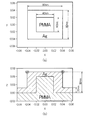
(1)試料分析素子の構造
図1は本発明の一実施形態に係る試料分析素子11を概略的に示す。この試料分析素子11すなわちセンサーチップは基板(基体)12を備える。基板12は例えば成型材料から形成される。成型材料には例えば樹脂材が使用されることができる。樹脂材にはポリメタクリル酸メチル樹脂(PMMA樹脂)といったアクリル樹脂が含まれることができる。
(1) Structure of Sample Analysis Element FIG. 1 schematically shows a
基板12の表面には金属膜13が形成される。金属膜13は金属から形成される。金属膜13は例えば銀から形成されることができる。その他、金属には金またはアルミニウムが用いられてもよい。金属膜13は例えば基板12の表面に一面に途切れなく形成されることができる。金属膜13は均一な膜厚で形成されることができる。金属膜13の膜厚は例えば20nm程度に設定されることができる。
A
金属膜13の表面にはナノ構造体15が形成される。ナノ構造体15は金属膜13の表面から突出する。ナノ構造体15は基板12の表面に分散する。個々のナノ構造体15は角柱に形成される。角柱の水平断面すなわち輪郭は例えば正方形に形成される。正方形の一辺の長さは例えば1〜1000nm程度に設定されることができる。角柱の高さ(金属膜13の表面から)は例えば10〜100nm程度で設定されることができる。角柱の水平断面は正方形以外の多角形に形成されてもよい。ナノ構造体15は円柱その他の立体形状に形成されてもよい。
A
ナノ構造体15はナノ構造体列16を形成する。個々のナノ構造体列16内でナノ構造体15は短ピッチSP(第1ピッチ)で金属膜13の表面に1列に配列される。ナノ構造体列16は第1方向SDに延びる。短ピッチSPは励起光の波長よりも小さく設定される。
The
ナノ構造体列16は第1方向SDに交差する第2方向DRに所定の長ピッチLP(第2ピッチ)で並列に並べられる。ここでは、第2方向DRは基板12の表面を含む1仮想平面内で第1方向SDに直交する。長ピッチLPは少なくとも短ピッチSPよりも大きく設定される。長ピッチLPの大きさは、後述されるように、エバネッセント波の波数に応じて設定される。
The
ナノ構造体列16同士の間には、ナノ構造体を含まない平面領域(ナノ構造体を含まない領域)17が形成される。すなわち、隣接するナノ構造体列16同士の間ではナノ構造体15の形成は排除される。
Between the
図2に示されるように、個々のナノ構造体15は誘電体の本体18を備える。本体18は角柱形状に形成される。本体18は基板12の表面から突き出る。本体18は基板12の材料と同一の材料から形成されることができる。本体18は基板12の表面に一体に形作られることができる。
As shown in FIG. 2, each
個々のナノ構造体15では本体18の表面は金属膜19で覆われる。金属膜19は金属膜13と同一の材料から形成されることができる。金属膜19および金属膜13は1枚の膜として形成されることができる。金属膜19は均一な膜厚で形成されることができる。
In each
試料分析素子11では、個々のナノ構造体15の大きさは励起光の波長よりも十分に小さく設定される。その結果、励起光の働きでナノ構造体15の金属膜19では局在表面プラズモン共鳴(LSPR)が引き起こされる。加えて、励起光の偏光面が第2方向DRに合わせ込まれると、長ピッチLPの設定に応じて、エバネッセント波に基づき伝播表面プラズモン共鳴(PSPR)が引き起こされる。伝播表面プラズモン共鳴はナノ構造体15の局在表面プラズモン共鳴に結合する。いわゆるハイブリッドモードが確立される。こうして局在表面プラズモン共鳴は伝播表面プラズモン共鳴で増強され、ナノ構造体15の金属膜19で近接場光は強められる。いわゆるホットスポットが形成される。しかも、個々のナノ構造体列16内ではナノ構造体15同士の間隔は長ピッチLPよりも小さい短ピッチSPに設定されることから、ナノ構造体15同士の間隔が長ピッチLPで設定される場合に比べてナノ構造体15の面密度は高められる。ホットスポットの面密度は高められる。
In the
(2)電場強度の検証
本発明者は試料分析素子11の電場強度を検証した。検証にあたってFDTD(Finite−Difference Time−Domain)法のシミュレーションソフトウェアが利用された。図3(a)および図3(b)に示されるように、本発明者はYee Cellに基づきシュミレーションモデルの単位ユニットを構築した。この単位ユニットでは120nm角のPMMA製基板12に銀の金属膜13が形成された。金属膜13の膜厚は20nmに設定された。PMMA製の本体18の輪郭は40nm角の正方形に設定された。本体18の高さ(基板12の表面から)は60nmに設定された。
(2) Verification of electric field strength The present inventors verified the electric field strength of the
図4(a)に示されるように、1列の単位ユニットすなわちナノ構造体15で1つのナノ構造体列16が構成された。複数のナノ構造体列16が平行に並べられた。x軸方向にナノ構造体列16の間に長ピッチLPが設定された。その結果、ナノ構造体列16同士の間には1列の空隙単位ユニットで平面領域17が形成された。空隙単位ユニットは120nm角の空隙で構成された。先頭のナノ構造体15で電場強度Exが算出された。周辺屈折率ns=1が設定された。直線偏光の励起光が設定された。偏光面はx軸方向に合わせられた。励起光は垂直入射に設定された。
As shown in FIG. 4A, one
図4(b)に示されるように、本発明者は比較モデルを用意した。比較モデルでは長ピッチLPは120nmに設定された。すなわち、平面領域17は省略された。単純にナノ構造体15が短ピッチSPで格子状に配置された。前述と同様に、選択された1つのナノ構造体15で電場強度Exが算出された。
As shown in FIG. 4B, the present inventor prepared a comparative model. In the comparative model, the long pitch LP was set to 120 nm. That is, the
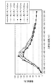
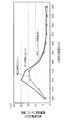
図5は電場強度Exに基づき作成された分散関係を示す。ここでは、単位面積当たりに換算された電場強度Exの二乗和が特定された。二乗和の特定にあたってナノ構造体15の上側の4つの頂点それぞれで電場強度Exが算出された。個々の頂点ごとに電場強度Exの二乗値が算出され、繰り返し計算の最小単位の全ての頂点の二乗値が足し合わせられた。単位面積として比較モデルの面積が設定された。足し合わせられた結果がその単位面積当たりに換算された。こうして単位面積当たり電場強度Exの二乗和が算出された。励起光の波長と二乗和との関係すなわち周波数特性が算出された。
FIG. 5 shows the dispersion relation created based on the electric field intensity Ex. Here, the sum of squares of the electric field intensity Ex converted per unit area was specified. In specifying the sum of squares, the electric field strength Ex was calculated at each of the four apexes on the upper side of the
図5で波数kは長ピッチLPに応じて特定される。直線21は空気(ns=1.0)の分散関係を示す。空気の分散関係は比例関係を示す。曲線22は屈折率(ns=1.0)の銀Agの伝播表面プラズモン共鳴の分散関係を示す。複数の長ピッチLP(=波数k)に現れる波長(=420nm)は局在表面プラズモン共鳴の共鳴波長に相当する。なぜならば、分散関係の傾きは伝搬表面プラズモンの移動速度を示し、複数の長ピッチPLで現れる角周波数の傾きは0(ゼロ)を示すからである。局在表面プラズモン共鳴の共鳴波長はナノ構造体15の体積や金属膜19の膜厚に応じて決定されることができる。いわゆるAnti−Crossing Behavior(ハイブリッドモードの指標として知られる)は観察されなかった。
In FIG. 5, the wave number k is specified according to the long pitch LP. A
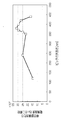
図6は電場強度Exの最大値を示す。比較モデルに対して長ピッチLPが増大すると電場強度Exの最大値は増大することが確認された。特に、長ピッチLP=380nmpで電場強度Exの最大値はピークを示すことが確認された。前述の分散関係から観察されるように、長ピッチLP=380nmpは局在表面プラズモン共鳴の分散関係と銀Agの伝播表面プラズモン共鳴の分散関係との交点に相当する。図7は電場強度Exの最大値の波長依存性を示す。長ピッチLPの大きさに拘わらず420nmの波長で電場強度Exの最大値はピークを示すことが確認された。図8は単位面積当たり電場強度Exの二乗和を示す。比較モデルに対して長ピッチLPが増大すると電場強度Exの二乗和が増大することが確認された。特に、長ピッチLP=380nmpで単位面積当たり電場強度Exの二乗和はピークを示すことが確認された。 FIG. 6 shows the maximum value of the electric field intensity Ex. It was confirmed that the maximum value of the electric field strength Ex increases as the long pitch LP increases with respect to the comparative model. In particular, it was confirmed that the maximum value of the electric field intensity Ex shows a peak at a long pitch LP = 380 nmp. As observed from the aforementioned dispersion relation, the long pitch LP = 380 nmp corresponds to the intersection of the dispersion relation of the localized surface plasmon resonance and the dispersion relation of the propagation surface plasmon resonance of silver Ag. FIG. 7 shows the wavelength dependence of the maximum value of the electric field intensity Ex. It was confirmed that the maximum value of the electric field intensity Ex shows a peak at a wavelength of 420 nm regardless of the size of the long pitch LP. FIG. 8 shows the square sum of the electric field strength Ex per unit area. It was confirmed that the square sum of the electric field intensity Ex increases as the long pitch LP increases with respect to the comparative model. In particular, it was confirmed that the square sum of the electric field intensity Ex per unit area shows a peak at a long pitch LP = 380 nmp.
図9(a)および図9(b)に示されるように、本発明者は第1比較単位ユニットを用意した。第1比較単位ユニットでは120nm角のシリコン(Si)製基板12の表面に銀の金属膜13が形成された。金属膜13の膜厚は20nmに設定された。ナノ構造体15の本体18は二酸化シリコン(SiO2)から形成された。その他の構造は前述の単位ユニットと同様に形成された。
As shown in FIGS. 9A and 9B, the present inventor prepared a first comparison unit. In the first comparative unit unit, a
本発明者は同様に第2比較単位ユニットを用意した。第2比較単位ユニットでは120nm角の二酸化シリコン(SiO2)製基板12の表面に銀の金属膜13が形成された。金属膜13の膜厚は20nmに設定された。ナノ構造体15の本体18は二酸化シリコン(SiO2)から形成された。すなわち、ナノ構造体15の本体18と基板12とは一体構造に設定された。その他の構造は前述の単位ユニットと同様に形成された。
The inventor similarly prepared a second comparison unit. In the second comparison unit unit, a
図10は電場強度Exの波長依存性を示す。波長依存性の特定にあたって単位ユニット、第1比較単位ユニットおよび第2比較単位ユニットで比較モデルが構築された。比較モデルで励起光の波長ごとに前述と同様に単位面積当たり電場強度Exの二乗和が算出された。このとき、二酸化シリコンの屈折率は1.45に設定されPMMAの屈折率は1.48に設定された。図10から明らかなように、第1比較単位ユニットでは単位ユニットおよび第2比較単位ユニットに対して電場強度Exの増強が観察された。単位ユニットと第2比較単位ユニットとの間では電場強度Exにほとんど差が観察されなかった。この結果から、第1比較単位ユニットではシリコン製基板12の表面から反射する戻り光の効果で電場強度Exが増大したことが容易く推測されることができる。その一方で、ナノ構造体15の本体18と基板12とが一体に形作られると、ナノ構造体15の本体18と基板12とは同一の材料から形成されることができる。ナノ構造体15の本体18と基板12とは一体成型で形成されることができる。試料分析素子11の製造工程は簡素化されることができる。試料分析素子11の量産性は高められることができる。一体成型の実施にあたってナノ構造体15および基板12は成型材料から形成されればよい。
FIG. 10 shows the wavelength dependence of the electric field intensity Ex. In identifying the wavelength dependence, a comparison model was constructed with the unit unit, the first comparison unit unit, and the second comparison unit unit. In the comparative model, the square sum of the electric field intensity Ex per unit area was calculated for each wavelength of the excitation light in the same manner as described above. At this time, the refractive index of silicon dioxide was set to 1.45, and the refractive index of PMMA was set to 1.48. As is clear from FIG. 10, in the first comparison unit unit, an increase in the electric field intensity Ex was observed with respect to the unit unit and the second comparison unit unit. Almost no difference in electric field intensity Ex was observed between the unit unit and the second comparison unit unit. From this result, it can be easily estimated that in the first comparison unit unit, the electric field intensity Ex has increased due to the effect of the return light reflected from the surface of the
(3)試料分析素子の製造方法
次に、試料分析素子11の製造方法を簡単に説明する。試料分析素子11の製造にあたってスタンパーが製造される。図11に示されるように、シリコン(Si)基板23の表面で二酸化シリコン(SiO2)の突起24が形成される。シリコン基板23の表面は平滑面に形成される。突起24は、基板12の表面に分散するナノ構造体15の本体18を象る。突起24の形成にあたって例えばリソグラフィ技術は用いられることができる。シリコン基板23の表面に一面に二酸化シリコン膜が形成される。二酸化シリコン膜の表面にナノ構造体15の本体18を象ったマスクが形成される。マスクには例えばフォトレジスト膜が用いられればよい。マスクの周囲で二酸化シリコン膜が除去されると、二酸化シリコン膜から個々の突起24は成形される。こうした成形にあたってエッチング処理やミリング処理が実施されればよい。
(3) Method for Manufacturing Sample Analysis Element Next, a method for manufacturing the
図12に示されるように、シリコン基板23の表面にニッケル(Ni)膜25が形成される。ニッケル膜25の形成にあたって無電解めっきが実施される。続いて、図13に示されるように、ニッケル膜25に基づき電鋳が実施される。シリコン基板23の表面には肉厚のニッケル板26が形成される。その後、図14に示されるように、ニッケル板26はシリコン基板23から剥離される。こうしてニッケル製のスタンパーは製造されることができる。ニッケル板26すなわちスタンパーの表面は平滑面に形成される。平滑面には突起24の剥離痕で窪み27が形成される。
As shown in FIG. 12, a nickel (Ni)
図15に示されるように、基板28は成型される。成型にあたって例えば成型材料の射出成型が利用されることができる。基板28の表面にはナノ構造体15の本体18が一体成型される。図16に示されるように、基板28の表面に一面に金属膜29が形成される。金属膜29の形成にあたって無電解めっきやスパッタリング、蒸着などが用いられることができる。こうして誘電体の本体18は金属膜19で覆われる。ナノ構造体15が形成される。その後、基板28から個々の基板12が切り出される。基板12の表面は金属膜13で覆われる。スタンパーは試料分析素子11の生産性の向上に大いに貢献することができる。
As shown in FIG. 15, the
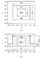
(4)一実施形態に係る検査装置
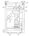
図17は一実施形態に係る標的分子検査装置(検査装置)101を概略的に示す。標的分子検査装置101は筐体102を備える。筐体102にはセンサーカートリッジ103が組み込まれる。センサーカートリッジ103には導入通路104と排出通路105とが個別に接続される。導入通路104からセンサーカートリッジ103に気体は導入される。センサーカートリッジ103から排出通路105に気体は排出される。導入通路104の通路入口106にはフィルター107が設置される。フィルター107は例えば気体中の塵埃や水蒸気を除去することができる。排出通路105の通路出口108には吸引ユニット109が設置される。吸引ユニット109は送風ファンで構成される。送風ファンの作動に応じて気体は導入通路104、センサーカートリッジ103および排出通路105を順番に流通する。こうした気体の流通経路内でセンサーカートリッジ103の前後にはシャッター(図示されず)が設置される。シャッターの開閉に応じてセンサーカートリッジ103内に気体は閉じ込められることができる。
(4) Testing Device According to One Embodiment FIG. 17 schematically shows a target molecule testing device (testing device) 101 according to one embodiment. The target
筐体102には識別センサー111が組み込まれる。識別センサー111はセンサーカートリッジ103の着脱を識別する。識別センサー111はセンサーカートリッジ103の装着および取り外しに応じて所定の電気信号を出力する。センサーカートリッジ103は例えば導入通路104および排出通路105に着脱自在に装着されることができる。
An
標的分子検査装置101はラマン散乱光検出ユニット112を備える。ラマン散乱光検出ユニット112は、センサーカートリッジ103に励起光を照射しラマン散乱光を検出する。ラマン散乱光検出ユニット112は筐体102内に遮光室113を区画する。遮光室113は周囲の光から遮断される。
The target
ラマン散乱光検出ユニット112は光源114を備える。光源114は遮光室113内に配置される。光源114にはレーザー光源が用いられることができる。レーザー光源は特定波長(単一波長)で直線偏光のレーザー光を放射することができる。
The Raman scattered
ラマン散乱光検出ユニット112は受光素子115を備える。受光素子115は例えば光の強度を検出することができる。受光素子115は光の強度に応じて検出電流を出力することができる。したがって、受光素子115から出力される電流の大きさに応じて光の強度は特定されることができる。
The Raman scattered
遮光室113内で、光源114とセンサーカートリッジ103との間、および、センサーカートリッジ103と受光素子115との間には光学系116が構築される。光学系116は光源114とセンサーカートリッジ103との間に光路を形成すると同時にセンサーカートリッジ103と受光素子115との間に光路を形成する。光学系116の働きで光源114の光はセンサーカートリッジ103に導かれる。センサーカートリッジ103の反射光は光学系116の働きで受光素子115に導かれる。
In the light shielding chamber 113, an
光学系116はコリメーターレンズ117、ダイクロイックミラー118、対物レンズ119、集光レンズ121、凹レンズ122、光学フィルター123および分光器124を備える。ダイクロイックミラー118は例えばセンサーカートリッジ103と受光素子115との間に配置される。対物レンズ119はダイクロイックミラー118とセンサーカートリッジ103との間に配置される。対物レンズ119はダイクロイックミラー118から供給される平行光を集光してセンサーカートリッジ103に導く。センサーカートリッジ103の反射光は対物レンズ119で平行光に変換されダイクロイックミラー118を透過する。ダイクロイックミラー118と受光素子115との間には集光レンズ121、凹レンズ122、光学フィルター123および分光器124が配置される。対物レンズ119、集光レンズ121および凹レンズ122の光軸は同軸に合わせ込まれる。集光レンズ121で集光された光は凹レンズ122で再び平行光に変換される。光学フィルター123はレイリー散乱光を除去する。ラマン散乱光は光学フィルター123を通過する。分光器124は例えば特定波長の光を選択的に透過させる。こうして受光素子115では特定波長ごとに光の強度が検出される。分光器124には例えばエタロンが用いられることができる。
The
光源114の光軸は対物レンズ119および集光レンズ121の光軸に直交する。ダイクロイックミラー118の表面はこれら光軸に45度の角度で交差する。ダイクロイックミラー118と光源114との間にはコリメーターレンズ117が配置される。こうしてコリメーターレンズ117は光源114に向き合わせられる。コリメーターレンズ117の光軸は光源114の光軸に同軸に合わせ込まれる。
The optical axis of the
標的分子検査装置101は制御ユニット126を備える。制御ユニット126に、識別センサー111、光源114、分光器124、受光素子115、吸引ユニット109、その他の機器が接続される。制御ユニット126は、光源114、分光器124および吸引ユニット109の動作を制御するとともに、識別センサー111および受光素子115の出力信号を処理する。制御ユニット126には信号コネクター127が接続される。制御ユニット126は信号コネクター127を通じて外部と信号をやりとりすることができる。
The target
標的分子検査装置101は電源ユニット128を備える。電源ユニット128は制御ユニット126に接続される。電源ユニット128は制御ユニット126に動作電力を供給する。制御ユニット126は電源ユニット128から電力の供給を受けて動作することができる。電源ユニット128には例えば1次電池や2次電池が用いられることができる。2次電池は、例えば、充電用の電源コネクター129を有することができる。
The target
制御ユニット126は信号処理制御部を備える。信号処理制御部は例えば中央演算処理装置(CPU)と、RAM(ランダムアクセスメモリー)やROM(リードオンリーメモリー)といった記憶回路で構成されることができる。ROMには例えば処理プログラムやスペクトルデータが格納されることができる。スペクトルデータでは標的分子のラマン散乱光のスペクトルが特定される。CPUは、一時的にRAMに処理プログラムやスペクトルデータを取り込みながら、処理プログラムを実行する。CPUは、スペクトルデータに、分光器および受光素子の働きで特定される光のスペクトルを照らし合わせる。
The
センサーカートリッジ103は筐体131を備える。筐体131は検出室132を区画する。検出室132は一端で導入通路104に接続され他端で排出通路105に接続される。筐体131にセンサーチップ11が組み込まれる。基体12の表面は検出室132の空間に接する。光源114から放出される光はコリメーターレンズ117で平行光に変換される。直線偏光の光はダイクロイックミラー118で反射する。反射した光は対物レンズ119で集光されてセンサーカートリッジ103に照射される。光はセンサーカートリッジ103の筐体131を透過してセンサーチップ11に到達する。このとき、光はセンサーチップ11の表面に直交する垂直方向に入射することができる。いわゆる垂直入射が確立されることができる。光の偏光面はナノ構造体列16(第1方向SD)に平行に合わせ込まれる。照射された光の働きでナノ構造体15の金属膜19では局在表面プラズモン共鳴が引き起こされる。ナノ構造体15同士の間で近接場光は強められる。いわゆるホットスポットが形成される。
The
このとき、ホットスポットでナノ構造体15に標的分子が付着すると、標的分子からレイリー散乱光およびラマン散乱光が生成される。いわゆる表面増強ラマン散乱が実現される。その結果、標的分子の種類に応じたスペクトルで光は対物レンズ119に向かって放出される。
At this time, when the target molecule adheres to the
こうしてセンサーカートリッジ103から放出される光は対物レンズ119で平行光に変換されダイクロイックミラー118、集光レンズ121、凹レンズ122および光学フィルター123を通過する。ラマン散乱光は分光器124に入射する。分光器124はラマン散乱光を分光する。こうして特定の波長ごとに受光素子115は光の強度を検出する。光のスペクトルはスペクトルデータに照らし合わせられる。光のスペクトルに応じて標的分子は検出されることができる。こうして標的分子検出装置101は表面増強ラマン散乱に基づき例えばアデノウィルスやライノウィルス、HIVウィルス、インフルエンザウィルスといった標的物質を検出することができる。
The light emitted from the
なお、上記のように本実施形態について詳細に説明したが、本発明の新規事項および効果から実体的に逸脱しない多くの変形が可能であることは当業者には容易に理解できるであろう。したがって、このような変形例はすべて本発明の範囲に含まれる。例えば、明細書または図面において、少なくとも一度、より広義または同義な異なる用語とともに記載された用語は、明細書または図面のいかなる箇所においても、その異なる用語に置き換えられることができる。また、試料分析素子11や標的物質検査装置101等の構成および動作も本実施形態で説明したものに限定されず、種々の変形が可能である。
Although the present embodiment has been described in detail as described above, it will be easily understood by those skilled in the art that many modifications can be made without departing from the novel matters and effects of the present invention. Therefore, all such modifications are included in the scope of the present invention. For example, a term described with a different term having a broader meaning or the same meaning at least once in the specification or the drawings can be replaced with the different term in any part of the specification or the drawings. Further, the configurations and operations of the
11 試料分析素子、12 基体、13 金属膜、15 ナノ構造体、16 ナノ構造体列、17 ナノ構造体を含まない領域(平面領域)、18 誘電体(本体)、19 金属膜、101 検査装置(標的分子検査装置)、103 センサーカートリッジ、114 光源、115 光検出器(受光素子)、131 筐体、SP 第1ピッチ(短ピッチ)、LP 第2ピッチ(長ピッチ)。
DESCRIPTION OF
Claims (8)
前記基体の表面に配列されて、金属膜で誘電体を覆う複数のナノ構造体と、を備え、
前記ナノ構造体は複数列のナノ構造体列を形成し、個々の前記ナノ構造体列では前記ナノ構造体は励起光の波長よりも小さい第1ピッチで第1方向に並べられ、前記ナノ構造体列は前記第1ピッチよりも大きい第2ピッチで前記第1方向とは交差する第2方向に並べられることを特徴とする試料分析素子。 A substrate;
A plurality of nanostructures arranged on the surface of the substrate and covering the dielectric with a metal film,
The nanostructures form a plurality of rows of nanostructures, and in each of the nanostructure rows, the nanostructures are arranged in a first direction at a first pitch smaller than the wavelength of excitation light, and the nanostructures The sample analysis element is characterized in that the body rows are arranged in a second direction intersecting the first direction at a second pitch larger than the first pitch.
前記ナノ構造体列に向けて光を放出する光源と、
前記光の照射に応じて前記ナノ構造体列から放射される光を検出する光検出器と
を備えることを特徴とする検査装置。 The sample analysis element according to any one of claims 1 to 6,
A light source that emits light toward the nanostructure array;
An inspection apparatus comprising: a photodetector that detects light emitted from the nanostructure array in response to the light irradiation.
前記検出室の空間に接する表面を有する基体と、
前記基体の表面に配列されて、金属膜で誘電体を覆う複数のナノ構造体と、を備え、
前記ナノ構造体は複数列のナノ構造体列を形成し、個々の前記ナノ構造体列では前記ナノ構造体は励起光の波長よりも小さい第1ピッチで第1方向に並べられ、前記ナノ構造体列は前記第1ピッチよりも大きい第2ピッチで前記第1方向とは交差する第2方向に並べられることを特徴とするセンサーカートリッジ。 A housing that divides the detection chamber;
A substrate having a surface in contact with the space of the detection chamber;
A plurality of nanostructures arranged on the surface of the substrate and covering the dielectric with a metal film,
The nanostructures form a plurality of rows of nanostructures, and in each of the nanostructure rows, the nanostructures are arranged in a first direction at a first pitch smaller than the wavelength of excitation light, and the nanostructures The body cartridge is arranged in a second direction that intersects the first direction at a second pitch that is larger than the first pitch.
Priority Applications (3)
| Application Number | Priority Date | Filing Date | Title |
|---|---|---|---|
| JP2012109188A JP2013234977A (en) | 2012-05-11 | 2012-05-11 | Sample analysis element, inspection device, and sensor cartridge |
| PCT/JP2013/002926 WO2013168404A1 (en) | 2012-05-11 | 2013-05-02 | Sample analyzing element and testing device and sensor cartridge |
| US14/400,193 US9222889B2 (en) | 2012-05-11 | 2013-05-02 | Sample analysis device, testing apparatus, and sensor cartridge |
Applications Claiming Priority (1)
| Application Number | Priority Date | Filing Date | Title |
|---|---|---|---|
| JP2012109188A JP2013234977A (en) | 2012-05-11 | 2012-05-11 | Sample analysis element, inspection device, and sensor cartridge |
Publications (2)
| Publication Number | Publication Date |
|---|---|
| JP2013234977A true JP2013234977A (en) | 2013-11-21 |
| JP2013234977A5 JP2013234977A5 (en) | 2015-06-25 |
Family
ID=49550468
Family Applications (1)
| Application Number | Title | Priority Date | Filing Date |
|---|---|---|---|
| JP2012109188A Withdrawn JP2013234977A (en) | 2012-05-11 | 2012-05-11 | Sample analysis element, inspection device, and sensor cartridge |
Country Status (3)
| Country | Link |
|---|---|
| US (1) | US9222889B2 (en) |
| JP (1) | JP2013234977A (en) |
| WO (1) | WO2013168404A1 (en) |
Families Citing this family (5)
| Publication number | Priority date | Publication date | Assignee | Title |
|---|---|---|---|---|
| JP2014169955A (en) | 2013-03-05 | 2014-09-18 | Seiko Epson Corp | Analysis device, analysis method, optical element and electronic apparatus used in them, and design method of optical element |
| JP6365817B2 (en) | 2014-02-17 | 2018-08-01 | セイコーエプソン株式会社 | Analytical device and electronic device |
| JP2015152492A (en) * | 2014-02-17 | 2015-08-24 | セイコーエプソン株式会社 | Analysis device and electronic apparatus |
| US11268854B2 (en) * | 2015-07-29 | 2022-03-08 | Samsung Electronics Co., Ltd. | Spectrometer including metasurface |
| JP6613736B2 (en) * | 2015-09-07 | 2019-12-04 | セイコーエプソン株式会社 | Substance detection method and substance detection apparatus |
Citations (3)
| Publication number | Priority date | Publication date | Assignee | Title |
|---|---|---|---|---|
| JP2009085724A (en) * | 2007-09-28 | 2009-04-23 | Canon Inc | Target substance detector and target substance detecting method |
| JP2009115492A (en) * | 2007-11-02 | 2009-05-28 | Canon Inc | Chemical sensor element, sensing device, and sensing method |
| JP2010256161A (en) * | 2009-04-24 | 2010-11-11 | Konica Minolta Holdings Inc | Plasmon excitation sensor, and assay method using the same |
Family Cites Families (35)
| Publication number | Priority date | Publication date | Assignee | Title |
|---|---|---|---|---|
| JP3452837B2 (en) | 1999-06-14 | 2003-10-06 | 理化学研究所 | Localized plasmon resonance sensor |
| JP4231701B2 (en) | 2002-01-08 | 2009-03-04 | 富士フイルム株式会社 | Plasmon resonance device |
| US7079250B2 (en) | 2002-01-08 | 2006-07-18 | Fuji Photo Film Co., Ltd. | Structure, structure manufacturing method and sensor using the same |
| US7399445B2 (en) | 2002-01-11 | 2008-07-15 | Canon Kabushiki Kaisha | Chemical sensor |
| JP3897703B2 (en) | 2002-01-11 | 2007-03-28 | キヤノン株式会社 | Sensor device and inspection method using the same |
| US7088449B1 (en) | 2002-11-08 | 2006-08-08 | The Board Of Trustees Of The Leland Stanford Junior University | Dimension measurement approach for metal-material |
| JP3957199B2 (en) | 2003-03-19 | 2007-08-15 | 富士フイルム株式会社 | Sensor chip, method of manufacturing sensor chip, and sensor using the sensor chip |
| EP1445601A3 (en) | 2003-01-30 | 2004-09-22 | Fuji Photo Film Co., Ltd. | Localized surface plasmon sensor chips, processes for producing the same, and sensors using the same |
| US7239076B2 (en) * | 2003-09-25 | 2007-07-03 | General Electric Company | Self-aligned gated rod field emission device and associated method of fabrication |
| BRPI0511255A (en) | 2004-05-19 | 2007-11-27 | Vp Holding Llc | layered plasmon structure optical sensor for enhanced detection of chemical groups by sers |
| JP4156567B2 (en) * | 2004-06-16 | 2008-09-24 | 日本電信電話株式会社 | SPR sensor and refractive index measuring method |
| CA2586197C (en) | 2004-11-04 | 2012-08-14 | Mesophotonics Limited | Metal nano-void photonic crystal for enhanced raman spectroscopy |
| JP2006208057A (en) | 2005-01-25 | 2006-08-10 | Taiyo Yuden Co Ltd | Plasmon resonance structure, its control method and manufacturing method of metal domain |
| US8835185B2 (en) | 2006-01-18 | 2014-09-16 | Canon Kabushiki Kaisha | Target substance-detecting element |
| JP2007218900A (en) | 2006-01-18 | 2007-08-30 | Canon Inc | Element for detecting target substance |
| JP2007240361A (en) | 2006-03-09 | 2007-09-20 | Sekisui Chem Co Ltd | Localized plasmon enhancing sensor |
| JP4994682B2 (en) | 2006-03-16 | 2012-08-08 | キヤノン株式会社 | Detection element, target substance detection apparatus using the detection element, and method for detecting target substance |
| JP5286515B2 (en) | 2006-05-11 | 2013-09-11 | 国立大学法人秋田大学 | Sensor chip and sensor chip manufacturing method |
| US8045141B2 (en) | 2006-05-12 | 2011-10-25 | Canon Kabushiki Kaisha | Detecting element, detecting device and detecting method |
| JP2008025989A (en) | 2006-07-15 | 2008-02-07 | Keio Gijuku | Ligand analyzing method due to localized surface plasmon resonance method and mass analyzing method, and sensor element therefor |
| GB2447696A (en) | 2007-03-23 | 2008-09-24 | Univ Exeter | Photonic biosensor arrays |
| WO2008136812A2 (en) | 2007-05-07 | 2008-11-13 | The Board Of Trustees Of The University Of Illinois | Fluorescence detection enhancement using photonic crystal extraction |
| JP5116362B2 (en) | 2007-05-28 | 2013-01-09 | 株式会社リコー | Biosensor |
| US7639355B2 (en) | 2007-06-26 | 2009-12-29 | Hewlett-Packard Development Company, L.P. | Electric-field-enhancement structure and detection apparatus using same |
| JP5080186B2 (en) | 2007-09-26 | 2012-11-21 | 富士フイルム株式会社 | Molecular analysis photodetection method, molecular analysis photodetection device used therefor, and sample plate |
| JP5175584B2 (en) | 2008-03-13 | 2013-04-03 | 地方独立行政法人 東京都立産業技術研究センター | Local surface plasmon resonance imaging system |
| WO2010039199A2 (en) | 2008-09-30 | 2010-04-08 | Pacific Biociences Of California, Inc. | Ultra-high multiplex analytical systems and methods |
| US8259381B2 (en) * | 2009-06-05 | 2012-09-04 | Exelis Inc. | Phase-change materials and optical limiting devices utilizing phase-change materials |
| US8415611B2 (en) | 2009-11-19 | 2013-04-09 | Seiko Epson Corporation | Sensor chip, sensor cartridge, and analysis apparatus |
| JP5621394B2 (en) | 2009-11-19 | 2014-11-12 | セイコーエプソン株式会社 | Sensor chip, sensor cartridge and analyzer |
| JP5589656B2 (en) | 2009-12-11 | 2014-09-17 | セイコーエプソン株式会社 | Sensor chip, sensor cartridge and analyzer |
| EP3943920B1 (en) | 2010-02-19 | 2024-04-03 | Pacific Biosciences Of California, Inc. | Integrated analytical system and method for fluorescence measurement |
| EP2372348A1 (en) | 2010-03-22 | 2011-10-05 | Imec | Methods and systems for surface enhanced optical detection |
| WO2012138915A1 (en) | 2011-04-05 | 2012-10-11 | Integrated Plasmonics Corporation | Integrated plasmonic sensing device and apparatus |
| US20140198314A1 (en) | 2011-10-18 | 2014-07-17 | Zhiyong Li | Molecular sensing device |
-
2012
- 2012-05-11 JP JP2012109188A patent/JP2013234977A/en not_active Withdrawn
-
2013
- 2013-05-02 WO PCT/JP2013/002926 patent/WO2013168404A1/en active Application Filing
- 2013-05-02 US US14/400,193 patent/US9222889B2/en not_active Expired - Fee Related
Patent Citations (3)
| Publication number | Priority date | Publication date | Assignee | Title |
|---|---|---|---|---|
| JP2009085724A (en) * | 2007-09-28 | 2009-04-23 | Canon Inc | Target substance detector and target substance detecting method |
| JP2009115492A (en) * | 2007-11-02 | 2009-05-28 | Canon Inc | Chemical sensor element, sensing device, and sensing method |
| JP2010256161A (en) * | 2009-04-24 | 2010-11-11 | Konica Minolta Holdings Inc | Plasmon excitation sensor, and assay method using the same |
Also Published As
| Publication number | Publication date |
|---|---|
| WO2013168404A1 (en) | 2013-11-14 |
| US9222889B2 (en) | 2015-12-29 |
| US20150138543A1 (en) | 2015-05-21 |
Similar Documents
| Publication | Publication Date | Title |
|---|---|---|
| WO2013157233A1 (en) | Sample analysis element and detection device | |
| WO2013168404A1 (en) | Sample analyzing element and testing device and sensor cartridge | |
| WO2013168401A1 (en) | Sensor chip, sensor cartridge and detection device | |
| JP5821511B2 (en) | Optical device and detection apparatus | |
| JP5923992B2 (en) | Sample analysis element and detection apparatus | |
| US8710427B2 (en) | Sensor chip, sensor cartridge, and analysis apparatus | |
| US8836946B2 (en) | Optical device and detection device | |
| US9488583B2 (en) | Molecular analysis device | |
| CN102401793B (en) | Optical device unit and detection apparatus | |
| US8045141B2 (en) | Detecting element, detecting device and detecting method | |
| JP5545144B2 (en) | Optical device unit and detection apparatus | |
| US20120062884A1 (en) | Detection apparatus | |
| WO2013161210A1 (en) | Sample analysis element and detection device | |
| JP5880064B2 (en) | Sample analysis element and detection apparatus | |
| US20140242573A1 (en) | Optical element, analysis device, analysis method and electronic apparatus | |
| JP5796395B2 (en) | Optical device, detection apparatus, and detection method | |
| JP2013195204A (en) | Sample analysis substrate and detector | |
| JP2016142617A (en) | Electric field enhancement element, analyzer, and electronic apparatus | |
| Sukhotskiy et al. | Numerical modelling of a sinusoidal grating-based surface plasmon coupled emission biosensor | |
| JP2015232526A (en) | Signal amplifier for raman spectroscopic analysis, raman spectroscopic analyzer, and raman spectroscopic analytical method | |
| JP2016004018A (en) | Raman spectrometer and electronic apparatus | |
| KR101669289B1 (en) | Sensor chip, sensor cartridge, and analysis apparatus | |
| JP2017040609A (en) | Sensor chip and manufacturing method therefor, and automatic analyzer | |
| JP2016197069A (en) | Electric field enhancement element, automatic analyzer and electronic apparatus |
Legal Events
| Date | Code | Title | Description |
|---|---|---|---|
| RD04 | Notification of resignation of power of attorney |
Free format text: JAPANESE INTERMEDIATE CODE: A7424 Effective date: 20150107 |
|
| A521 | Written amendment |
Free format text: JAPANESE INTERMEDIATE CODE: A523 Effective date: 20150501 |
|
| A621 | Written request for application examination |
Free format text: JAPANESE INTERMEDIATE CODE: A621 Effective date: 20150501 |
|
| A131 | Notification of reasons for refusal |
Free format text: JAPANESE INTERMEDIATE CODE: A131 Effective date: 20160426 |
|
| A761 | Written withdrawal of application |
Free format text: JAPANESE INTERMEDIATE CODE: A761 Effective date: 20160601 |